EP1130677A2 - Patch antenna with finite ground plane - Google Patents
Patch antenna with finite ground plane Download PDFInfo
- Publication number
- EP1130677A2 EP1130677A2 EP01301456A EP01301456A EP1130677A2 EP 1130677 A2 EP1130677 A2 EP 1130677A2 EP 01301456 A EP01301456 A EP 01301456A EP 01301456 A EP01301456 A EP 01301456A EP 1130677 A2 EP1130677 A2 EP 1130677A2
- Authority
- EP
- European Patent Office
- Prior art keywords
- ground plane
- feed line
- antenna
- signal feed
- patch element
- Prior art date
- Legal status (The legal status is an assumption and is not a legal conclusion. Google has not performed a legal analysis and makes no representation as to the accuracy of the status listed.)
- Withdrawn
Links
Images


Classifications
-
- H—ELECTRICITY
- H01—ELECTRIC ELEMENTS
- H01Q—ANTENNAS, i.e. RADIO AERIALS
- H01Q13/00—Waveguide horns or mouths; Slot antennas; Leaky-waveguide antennas; Equivalent structures causing radiation along the transmission path of a guided wave
- H01Q13/08—Radiating ends of two-conductor microwave transmission lines, e.g. of coaxial lines, of microstrip lines
-
- H—ELECTRICITY
- H01—ELECTRIC ELEMENTS
- H01Q—ANTENNAS, i.e. RADIO AERIALS
- H01Q9/00—Electrically-short antennas having dimensions not more than twice the operating wavelength and consisting of conductive active radiating elements
- H01Q9/04—Resonant antennas
- H01Q9/0407—Substantially flat resonant element parallel to ground plane, e.g. patch antenna
-
- H—ELECTRICITY
- H01—ELECTRIC ELEMENTS
- H01Q—ANTENNAS, i.e. RADIO AERIALS
- H01Q19/00—Combinations of primary active antenna elements and units with secondary devices, e.g. with quasi-optical devices, for giving the antenna a desired directional characteristic
- H01Q19/10—Combinations of primary active antenna elements and units with secondary devices, e.g. with quasi-optical devices, for giving the antenna a desired directional characteristic using reflecting surfaces
-
- H—ELECTRICITY
- H01—ELECTRIC ELEMENTS
- H01Q—ANTENNAS, i.e. RADIO AERIALS
- H01Q3/00—Arrangements for changing or varying the orientation or the shape of the directional pattern of the waves radiated from an antenna or antenna system
- H01Q3/12—Arrangements for changing or varying the orientation or the shape of the directional pattern of the waves radiated from an antenna or antenna system using mechanical relative movement between primary active elements and secondary devices of antennas or antenna systems
- H01Q3/16—Arrangements for changing or varying the orientation or the shape of the directional pattern of the waves radiated from an antenna or antenna system using mechanical relative movement between primary active elements and secondary devices of antennas or antenna systems for varying relative position of primary active element and a reflecting device
- H01Q3/20—Arrangements for changing or varying the orientation or the shape of the directional pattern of the waves radiated from an antenna or antenna system using mechanical relative movement between primary active elements and secondary devices of antennas or antenna systems for varying relative position of primary active element and a reflecting device wherein the primary active element is fixed and the reflecting device is movable
-
- H—ELECTRICITY
- H01—ELECTRIC ELEMENTS
- H01Q—ANTENNAS, i.e. RADIO AERIALS
- H01Q9/00—Electrically-short antennas having dimensions not more than twice the operating wavelength and consisting of conductive active radiating elements
- H01Q9/04—Resonant antennas
- H01Q9/0407—Substantially flat resonant element parallel to ground plane, e.g. patch antenna
- H01Q9/045—Substantially flat resonant element parallel to ground plane, e.g. patch antenna with particular feeding means
- H01Q9/0457—Substantially flat resonant element parallel to ground plane, e.g. patch antenna with particular feeding means electromagnetically coupled to the feed line
Definitions
- the present invention relates generally to improvements to antennas, and more particularly to advantageous aspects of a patch antenna with a finite ground plane.
- microstrip patch antenna In a microstrip patch antenna, the radiator is typically provided by a metallic patch element that has been fabricated, using microstrip techniques, onto a dielectric substrate above a ground plane. Because of their low profile, low cost, and compact size, microstrip patch antennas are suitable for various microwave antenna and antenna array applications. Microstrip patch antennas are used, for example, as the radiating elements of designs based on a microwave integrated circuit (MIC) or monolithic microwave integrated circuit (MMIC) such as those used in aircraft and satellite communications, in missile and rocket antenna systems, as well as personal communication system (PCS) wireless applications.
- MIC microwave integrated circuit
- MMIC monolithic microwave integrated circuit
- PCS personal communication system
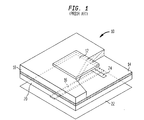
- Fig. 1 shows a cutaway perspective view of a microstrip patch antenna 10 according to the prior art.
- the antenna 10 comprises a square patch element 12, a ground plane 14, and a microstrip feed line 16, lying on parallel planes defined by the top and bottom surfaces of a pair of dielectric substrates 18 and 20.
- the patch element 12 is fabricated onto the top surface of the upper substrate 18, the ground plane 14 is fabricated between the bottom surface of the upper substrate 18 and the top surface of the lower substrate 20, and the feed line 16 is fabricated onto the bottom surface of the lower substrate 20.
- a fixed metal plate reflector 22 is provided at the bottom of the antenna 10 to reflect radiation towards the top of the antenna 10.
- Coupling between the feed line 16 and the patch element 12 is provided by a small rectangular aperture 24 in the ground plane 14 that lies across the feed line 16. Because of this coupling technique, the design shown in Fig. 1 is known as an "aperture-coupled patch antenna.” Other designs are also used, employing different techniques to couple the feed line to the patch element.
- the ground plane 14 is significantly larger than the aperture 24 such that, from an electromagnetic perspective, the ground plane 14 functions as an infinite surface relative to the aperture 24. This helps the isolation between the feed line 16 and the patch element 12. In addition, the use of an infinite ground plane makes analysis of the antenna much easier because the equivalence theorem can be applied.
- An antenna's radiation pattern is important in antenna applications. It includes several parameters to characterize the antenna performance, including gain, 3 dB (half-power) beamwidth, side-lobe level, front-to-back (F/B) ratio, polarization, cross-polarization level, and the line.
- the 3 dB beamwidth parameter is the main parameter to show the coverage of radiated energy.
- the beamwidth of a conventional patch antenna is approximately 60° to 70°.
- TDMA time division multiple access
- CDMA code division multiple access
- a dipole element with an angular reflector can be employed to provide beamwidth control by mechanically adjusting the reflector angle.
- this approach requires sophisticated mechanical structures which may not be cost effective, and which may also result in an undesirably large package size to accommodate these structures.
- the antenna comprises a patch element and a ground plane separated from the patch element by a first dielectric layer.
- the antenna further includes a signal feed line separated from the ground plane by a second dielectric layer, the signal feed line being shielded from the patch element by the ground plane.
- the signal feed line is electromagnetically coupled to the patch element through an aperture in the ground plane lying across the signal feed line, the ground plane functioning as a finite surface relative to the aperture.
- the beamwidth of the antenna is adjusted by adjusting the position of a reflector behind the signal feed line.
- Fig. 1 shows a partial cutaway perspective view of a microstrip patch antenna according to the prior art.
- Fig. 2 shows a partial cutaway perspective view of a first embodiment of a microstrip patch antenna according to the present invention.
- Figs. 3A through 3D show, respectively, top, side, front, and bottom views of a further embodiment of a microstrip patch antenna according to the present invention.
- Fig. 4 shows a bottom view of the top substrate layer of the antenna shown in Figs. 3A through 3D.
- Figs. 5A through 5C show, respectively, top, bottom, and side views of the bottom substrate layer of the antenna shown in Figs. 3A through 3D.
- the antenna has a patch element, a ground plane separated from the patch element by a first dielectric layer, and a signal feed line separated from the ground plane by a second dielectric layer.
- the signal feed line is shielded from the patch element by the ground plane, and the signal feed line is electromagnetically coupled to the patch element through an aperture in the ground plane lying across the signal feed line.
- the ground plane functions as a finite surface relative to the aperture.
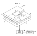
- Fig. 2 shows a partial cutaway perspective view of a first embodiment of a patch antenna 30 according to the present invention.
- the Fig. 2 patch antenna 30 includes a patch element 32, a finite ground plane 34, and a microstrip feed line 36 lying on parallel planes defined by upper and lower substrates 38 and 40.
- a reflector 42 is provided to reflect radiation towards the top of the antenna 30.
- the patch element 32 is coupled to the microstrip feed line 36 by a rectangular aperture 44 in the finite ground plane 34.
- the dimensions of the finite ground plane 34 are chosen such that it behaves as a finite surface relative to the aperture 44.
- the upper limit of the ground plane width is dictated by the edge diffraction conditions which, in the present embodiment of the invention, are derived from the distance of the edges of the ground plane 34 to the radiation caustic, namely, the patch element 32. Therefore, in the present embodiment of the invention, the definition of the "finite" ground plane 34 is that the width of the ground plane 34 is less than one-half wavelength of the operation frequency (0.5 ⁇ ) to allow measurable beamwidth variation due to variant reflector positions. Also, the width of the ground plane 34 is more than 1.5 times the width of the patch element 32 to allow a good voltage standing wave ratio (VSWR) performance.
- VSWR voltage standing wave ratio
- the finite ground plane 34 significantly enhances the beamwidth of the antenna 30.
- the beamwidth of the antenna can be increased to 85°.
- the beamwidth capabilities of the antenna 30 are further improved by modifying the shape of the patch element 32.
- the patch element is typically square.
- the use of the rectangular patch element 32 in combination with the finite ground plane 34 has been shown to increase the beamwidth of the antenna 30 to 90°
- the Fig. 2 antenna 30 provides a system for adjusting the antenna beamwidth.
- a finite ground plane 34 it has been found that it is possible to adjust the beamwidth of the antenna 30 by adjusting the position of the reflector 42 relative to the microstrip feed line 36. Moving the reflector 42 away the feed line 36 increases the "spill" of radiation around the reflector, thereby resulting in an increase in beamwidth.
- the beamwidth can be adjusted to any value in the range of 80° to 110°, without de-tuning the antenna's impedance matching.
- adjustment of the reflector is accomplished by mounting the reflector 42 to a digital stepper motor 46 that is operated by a microprocessor controller 48. It will be recognized that other spacing control adjusters may be devised and suitably utilized.
- the present invention provides an efficient way to achieve adjustable wide-beamwidth (between 80° and 110°) for various wireless systems in a three-sector configuration, which requires coverage of a 120° geographic area. It not only extends the beamwidth of a traditional patch antenna from 60°-70° to over 90°, but also provides a readily adjustable beamwidth.
- the invention thus allows patch antennas to be used in applications such as three-sector base station radiators.
- the conventional dipole antennas can be replaced by these low-cost, low-profile, and highly-integrated patch antennas.
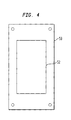
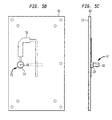
- Figs. 3A through 3D show, respectively, top, right side, front, and bottom views of a further embodiment of an antenna 50 according to the present invention.
- the antenna includes a patch element 52, a finite ground plane 54, and a microstrip feed line 56 that are laid onto upper and lower dielectric substrates 58 and 60.
- the patch element 52 shown in greater detail in Fig. 4, is a relatively narrow rectangle that is fabricated onto the bottom surface of the upper dielectric substrate 58.
- the finite ground plane 54 shown in greater detail in Fig.5A, is fabricated onto the top surface of the lower dielectric substrate 60.
- the microstrip feed line 56 shown in greater detail in Fig. 5B, is fabricated onto the bottom surface of the lower dielectric substrate 60.
- the microstrip feed line 56 is fed by a coaxial feed 62, the outer conductor 64 of which is electrically connected to the finite ground plane 54 and the inner conductor 66 of which is electrically connected to the microstrip feed line 66.
- a metal reflector 68 is provided to reflect radiation towards the top of the antenna 50.
- the reflector 68 includes a first pair of wing members 70 extending upward around the lower substrate 60 and a second pair of wing members 72 extending downward around the coaxial feed 62. As shown in Fig. 3D, the reflector 68 includes a hole 88 through which the coaxial feed 62 passes.
- the upper and lower substrates 58 and 60 are separated from each other by a set of four spacers 84. This creates a layer of air between the patch element 52 and the ground plane 54. If desired, the layer of air can be replaced by a solid substrate.
- a second set of four spacers 86 is used to separate the lower substrate 60 from the reflector plate 68.
- the four spacers 84 are replaced by a movable mounting assembly that allows the reflector plate 68 to be moved precisely relative to the upper and lower substrates 58 and 60 while maintaining a parallel relationship with those elements. In that embodiment, the movement of the reflector plate 68 is controlled using a microprocessor-controlled stepper motor, as shown in Fig. 2.
- Fig. 4 shows a bottom view of the upper substrate 58 with the metallic patch element 52 fabricated thereon.
- the shape of the patch element 52 is a relatively narrow rectangle having a width that is 60% or less of its length.
- Fig. 5A shows a top view of the lower substrate 60.
- the finite ground plane 54 is fabricated onto the substrate 60, and includes at its center a rectangular aperture 90.
- the aperture 90 only extends through the ground plane 54. It does not extend through the substrate 60, although it would be possible to do so, if desired.
- the size of the ground plane 54 relative to the aperture 90 is such that the ground plane 54 functions as a finite surface with respect to the aperture 90.
- Figs. 5B and 5C show, respectively, bottom and side views of the lower substrate 60.
- the microstrip feed line 56 is fabricated directly onto the bottom surface of the lower substrate 60 and extends across the aperture 90 in the ground plane 54. As mentioned above, the aperture 90 does not extend all the way through the substrate 60.
- the coaxial feed 62 is mounted perpendicular to the lower substrate 60. Its inner conductor 66 is electrically connected to the microstrip feed line 56. Its outer conductor 64 extends through the lower substrate 60 and is electrically connected to the ground plane 54 on the other side of the substrate 60.
Abstract
Description
- The present invention relates generally to improvements to antennas, and more particularly to advantageous aspects of a patch antenna with a finite ground plane.
- In a microstrip patch antenna, the radiator is typically provided by a metallic patch element that has been fabricated, using microstrip techniques, onto a dielectric substrate above a ground plane. Because of their low profile, low cost, and compact size, microstrip patch antennas are suitable for various microwave antenna and antenna array applications. Microstrip patch antennas are used, for example, as the radiating elements of designs based on a microwave integrated circuit (MIC) or monolithic microwave integrated circuit (MMIC) such as those used in aircraft and satellite communications, in missile and rocket antenna systems, as well as personal communication system (PCS) wireless applications. However, one problem associated with microstrip patch antennas is that they typically have a limited beamwidth, compared with, for example, antenna designs employing a dipole element. In addition, current microstrip patch antenna designs do not provide for a compact, cost-efficient mechanism for adjusting the antenna beamwidth.
- The prior art can be better understood with reference to Fig. 1, which shows a cutaway perspective view of a
microstrip patch antenna 10 according to the prior art. As shown in Fig. 1, theantenna 10 comprises asquare patch element 12, aground plane 14, and amicrostrip feed line 16, lying on parallel planes defined by the top and bottom surfaces of a pair ofdielectric substrates patch element 12 is fabricated onto the top surface of theupper substrate 18, theground plane 14 is fabricated between the bottom surface of theupper substrate 18 and the top surface of thelower substrate 20, and thefeed line 16 is fabricated onto the bottom surface of thelower substrate 20. A fixedmetal plate reflector 22 is provided at the bottom of theantenna 10 to reflect radiation towards the top of theantenna 10. Coupling between thefeed line 16 and thepatch element 12 is provided by a smallrectangular aperture 24 in theground plane 14 that lies across thefeed line 16. Because of this coupling technique, the design shown in Fig. 1 is known as an "aperture-coupled patch antenna." Other designs are also used, employing different techniques to couple the feed line to the patch element. - In current aperture-coupled patch antenna designs, the
ground plane 14 is significantly larger than theaperture 24 such that, from an electromagnetic perspective, theground plane 14 functions as an infinite surface relative to theaperture 24. This helps the isolation between thefeed line 16 and thepatch element 12. In addition, the use of an infinite ground plane makes analysis of the antenna much easier because the equivalence theorem can be applied. - An antenna's radiation pattern is important in antenna applications. It includes several parameters to characterize the antenna performance, including gain, 3 dB (half-power) beamwidth, side-lobe level, front-to-back (F/B) ratio, polarization, cross-polarization level, and the line. The 3 dB beamwidth parameter is the main parameter to show the coverage of radiated energy. The beamwidth of a conventional patch antenna is approximately 60° to 70°.
- Because of their high level of integration, patch antennas have been used successfully to form large arrays for highly directional applications. However, other applications require a beam width of greater than the currently available 60° to 70°. For example, a typical three-section cellular system needs to cover a 120° geographic area. In a time division multiple access (TDMA) system, the base station requires an antenna with a 3 dB beamwidth of 105° to 110°, and a code division multiple access (CDMA) system requires a 3 dB beamwidth of 90°. Because of the beamwidth limitations of conventional patch elements, a dipole element is typically used instead in these applications.
- In addition, it is desirable for the beamwidth of an antenna to be adjustable in certain applications. A dipole element with an angular reflector can be employed to provide beamwidth control by mechanically adjusting the reflector angle. However, this approach requires sophisticated mechanical structures which may not be cost effective, and which may also result in an undesirably large package size to accommodate these structures.
- One aspect of the invention provides a microstrip patch antenna with enhanced beamwidth characteristics. In a first embodiment, the antenna comprises a patch element and a ground plane separated from the patch element by a first dielectric layer. The antenna further includes a signal feed line separated from the ground plane by a second dielectric layer, the signal feed line being shielded from the patch element by the ground plane. The signal feed line is electromagnetically coupled to the patch element through an aperture in the ground plane lying across the signal feed line, the ground plane functioning as a finite surface relative to the aperture. According to a further aspect of the invention, the beamwidth of the antenna is adjusted by adjusting the position of a reflector behind the signal feed line. Thus, the present invention provides an efficient way to achieve adjustable wide-beamwidth that may be used, for example, in wireless systems in a three-sector configuration.
- Additional features and advantages of the present invention will become apparent by reference to the following detailed description and accompanying drawings.
- Fig. 1 shows a partial cutaway perspective view of a microstrip patch antenna according to the prior art.
- Fig. 2 shows a partial cutaway perspective view of a first embodiment of a microstrip patch antenna according to the present invention.
- Figs. 3A through 3D show, respectively, top, side, front, and bottom views of a further embodiment of a microstrip patch antenna according to the present invention.
- Fig. 4 shows a bottom view of the top substrate layer of the antenna shown in Figs. 3A through 3D.
- Figs. 5A through 5C show, respectively, top, bottom, and side views of the bottom substrate layer of the antenna shown in Figs. 3A through 3D.
- One aspect of the present invention provides a microstrip patch antenna with enhanced beamwidth capabilities. The antenna has a patch element, a ground plane separated from the patch element by a first dielectric layer, and a signal feed line separated from the ground plane by a second dielectric layer. The signal feed line is shielded from the patch element by the ground plane, and the signal feed line is electromagnetically coupled to the patch element through an aperture in the ground plane lying across the signal feed line. As explained below, according to the present invention, the ground plane functions as a finite surface relative to the aperture.
- Fig. 2 shows a partial cutaway perspective view of a first embodiment of a
patch antenna 30 according to the present invention. The Fig. 2patch antenna 30 includes apatch element 32, afinite ground plane 34, and amicrostrip feed line 36 lying on parallel planes defined by upper andlower substrates reflector 42 is provided to reflect radiation towards the top of theantenna 30. Thepatch element 32 is coupled to themicrostrip feed line 36 by arectangular aperture 44 in thefinite ground plane 34. - The dimensions of the
finite ground plane 34 are chosen such that it behaves as a finite surface relative to theaperture 44. The upper limit of the ground plane width is dictated by the edge diffraction conditions which, in the present embodiment of the invention, are derived from the distance of the edges of theground plane 34 to the radiation caustic, namely, thepatch element 32. Therefore, in the present embodiment of the invention, the definition of the "finite"ground plane 34 is that the width of theground plane 34 is less than one-half wavelength of the operation frequency (0.5λ) to allow measurable beamwidth variation due to variant reflector positions. Also, the width of theground plane 34 is more than 1.5 times the width of thepatch element 32 to allow a good voltage standing wave ratio (VSWR) performance. - Although the use of a finite ground plane complicates the analysis of the
antenna 30, it has been found that thefinite ground plane 34 significantly enhances the beamwidth of theantenna 30. As addressed further below, it has been found that by using a suitably dimensioned finite ground plane, the beamwidth of the antenna can be increased to 85°. - It has also been found that the beamwidth capabilities of the
antenna 30 are further improved by modifying the shape of thepatch element 32. In current patch antennas, the patch element is typically square. However, it has been found that with afinite ground plane 34, it is advantageous to use arectangular patch element 32, where the width of thepatch element 34 is 60 percent of its length or narrower. (It should be noted that, in a wide beamwidth application, the 60 percent width satisfies the above criteria for a finite ground plane.) The use of therectangular patch element 32 in combination with thefinite ground plane 34 has been shown to increase the beamwidth of theantenna 30 to 90° - Further, the Fig. 2
antenna 30 provides a system for adjusting the antenna beamwidth. Using afinite ground plane 34, it has been found that it is possible to adjust the beamwidth of theantenna 30 by adjusting the position of thereflector 42 relative to themicrostrip feed line 36. Moving thereflector 42 away thefeed line 36 increases the "spill" of radiation around the reflector, thereby resulting in an increase in beamwidth. By carefully adjusting the reflector height, the beamwidth can be adjusted to any value in the range of 80° to 110°, without de-tuning the antenna's impedance matching. In the present embodiment of the invention, shown in Fig. 2, adjustment of the reflector is accomplished by mounting thereflector 42 to adigital stepper motor 46 that is operated by amicroprocessor controller 48. It will be recognized that other spacing control adjusters may be devised and suitably utilized. - Thus, the present invention provides an efficient way to achieve adjustable wide-beamwidth (between 80° and 110°) for various wireless systems in a three-sector configuration, which requires coverage of a 120° geographic area. It not only extends the beamwidth of a traditional patch antenna from 60°-70° to over 90°, but also provides a readily adjustable beamwidth. The invention thus allows patch antennas to be used in applications such as three-sector base station radiators. Thus, the conventional dipole antennas can be replaced by these low-cost, low-profile, and highly-integrated patch antennas.
- Further, using the present invention, it is possible to engineer cell boundaries in a cellular network to be adjustable, such that cell loading can be properly managed and optimized depending upon such variables as the time of day, season, and geographical area. This approach can be realized by employing a base station antenna with the above-described beamwidth control capability.
- Figs. 3A through 3D show, respectively, top, right side, front, and bottom views of a further embodiment of an
antenna 50 according to the present invention. The antenna includes apatch element 52, afinite ground plane 54, and amicrostrip feed line 56 that are laid onto upper and lowerdielectric substrates patch element 52, shown in greater detail in Fig. 4, is a relatively narrow rectangle that is fabricated onto the bottom surface of the upperdielectric substrate 58. Thefinite ground plane 54, shown in greater detail in Fig.5A, is fabricated onto the top surface of the lowerdielectric substrate 60.
Themicrostrip feed line 56, shown in greater detail in Fig. 5B, is fabricated onto the bottom surface of the lowerdielectric substrate 60. Themicrostrip feed line 56 is fed by acoaxial feed 62, theouter conductor 64 of which is electrically connected to thefinite ground plane 54 and theinner conductor 66 of which is electrically connected to themicrostrip feed line 66. Finally, ametal reflector 68 is provided to reflect radiation towards the top of theantenna 50. Thereflector 68 includes a first pair ofwing members 70 extending upward around thelower substrate 60 and a second pair ofwing members 72 extending downward around thecoaxial feed 62. As shown in Fig. 3D, thereflector 68 includes ahole 88 through which thecoaxial feed 62 passes. - In the present embodiment of the antenna, the upper and
lower substrates spacers 84. This creates a layer of air between thepatch element 52 and theground plane 54. If desired, the layer of air can be replaced by a solid substrate. A second set of fourspacers 86 is used to separate thelower substrate 60 from thereflector plate 68. In an embodiment of the invention in which thereflector plate 68 is adjustable, the fourspacers 84 are replaced by a movable mounting assembly that allows thereflector plate 68 to be moved precisely relative to the upper andlower substrates reflector plate 68 is controlled using a microprocessor-controlled stepper motor, as shown in Fig. 2. - Fig. 4 shows a bottom view of the
upper substrate 58 with themetallic patch element 52 fabricated thereon. As discussed above, according to the present invention the shape of thepatch element 52 is a relatively narrow rectangle having a width that is 60% or less of its length. However, it would also be possible to practice the present invention using asquare patch element 52. - Fig. 5A shows a top view of the
lower substrate 60. Thefinite ground plane 54 is fabricated onto thesubstrate 60, and includes at its center arectangular aperture 90. In the embodiment shown in Fig. 5A, theaperture 90 only extends through theground plane 54. It does not extend through thesubstrate 60, although it would be possible to do so, if desired. As discussed above, the size of theground plane 54 relative to theaperture 90 is such that theground plane 54 functions as a finite surface with respect to theaperture 90. - Figs. 5B and 5C show, respectively, bottom and side views of the
lower substrate 60. Themicrostrip feed line 56 is fabricated directly onto the bottom surface of thelower substrate 60 and extends across theaperture 90 in theground plane 54. As mentioned above, theaperture 90 does not extend all the way through thesubstrate 60. Thecoaxial feed 62 is mounted perpendicular to thelower substrate 60. Itsinner conductor 66 is electrically connected to themicrostrip feed line 56. Itsouter conductor 64 extends through thelower substrate 60 and is electrically connected to theground plane 54 on the other side of thesubstrate 60. - While the foregoing description includes details which will enable those skilled in the art to practice the invention, it should be recognized that the description is illustrative in nature and that many modifications and variations thereof will be apparent to those skilled in the art having the benefit of these teachings. It is accordingly intended that the invention herein be defined solely by the claims appended hereto and that the claims be interpreted as broadly as permitted by the prior art.
Claims (13)
- An antenna, comprising:a patch element;a ground plane separated from the patch element by a first dielectric layer;a signal feed line separated from the ground plane by a second dielectric layer, the signal feed line being shielded from the patch element by the ground plane;the signal feed line being electromagnetically coupled to the patch element through an aperture in the ground plane lying across the signal feed line, the ground plane functioning as a finite surface relative to the aperture.
- The antenna of claim 1, further including a coaxial feed, the outer conductor of which is connected to the ground plane and the inner conductor of which is connected to the signal feed line.
- An antenna, comprising:a patch element fabricated onto the top surface of a first substrate;a ground plane fabricated between the bottom surface of the first substrate and the top surface of a second substrate; anda signal feed line fabricated onto the bottom surface of the second substrate,the signal feed line being coupled to the patch element through an aperture in the ground plane lying across the signal feed line, the ground plane functioning as a finite surface relative to the aperture.
- An antenna, comprising:a patch element fabricated onto the bottom surface of a first substrate;a ground plane fabricated onto the top surface of a second substrate, the patch element and the ground plane being separated by a layer of air;a signal feed line fabricated onto the bottom surface of the second substrate,the signal feed line being coupled to the patch element through an aperture in the ground plane lying across the signal feed line, the ground plane functioning as a finite surface relative to the aperture.
- The antenna of claim 1,3 or 4 wherein the width of the ground plane is less than one-half wavelength of the operation frequency, thereby allowing measurable beamwidth variation due to variant reflector positions.
- The antenna of claim 1,3 or 4 wherein the patch element is a rectangle having a width that is 60 percent or less of its length.
- The antenna of claim 1,3 or 4 further including:
a reflector proximate to the signal feed line for reflecting radiation from the signal feed line, the reflector being positioned such that the signal feed line is between the ground plane and the reflector. - The antenna of claim 1,3 or 4 wherein the position of the reflector is adjustable, an adjustment of the position of the reflector producing a change in the antenna beamwidth.
- The antenna of claim 8 wherein the position of the reflector is adjusted by a stepper motor.
- The antenna of claim 9 wherein the stepper motor is operated by a microprocessor controller.
- A method for manufacturing an antenna, comprising the following steps:(a) fabricating a patch element onto a first surface;(b) fabricating a signal feed line onto a second surface;(c) separating the patch element from the signal feed line by a ground plane;(d) electromagnetically coupling the signal feed line with the patch element through an aperture in the ground plane lying across the signal feed line, the ground plane functioning as a finite surface relative to the aperture.
- The method of claim 11, further including:
(e) positioning a reflector such that the signal feed line is between the ground plane and the reflector. - The method of claim 12 further including:
(f) adjusting the antenna beamwidth by adjusting the position of the reflector.
Applications Claiming Priority (2)
| Application Number | Priority Date | Filing Date | Title |
|---|---|---|---|
| US09/515,950 US6335703B1 (en) | 2000-02-29 | 2000-02-29 | Patch antenna with finite ground plane |
| US515950 | 2000-02-29 |
Publications (2)
| Publication Number | Publication Date |
|---|---|
| EP1130677A2 true EP1130677A2 (en) | 2001-09-05 |
| EP1130677A3 EP1130677A3 (en) | 2003-10-15 |
Family
ID=24053473
Family Applications (1)
| Application Number | Title | Priority Date | Filing Date |
|---|---|---|---|
| EP01301456A Withdrawn EP1130677A3 (en) | 2000-02-29 | 2001-02-19 | Patch antenna with finite ground plane |
Country Status (9)
| Country | Link |
|---|---|
| US (1) | US6335703B1 (en) |
| EP (1) | EP1130677A3 (en) |
| JP (1) | JP2001284951A (en) |
| KR (1) | KR20010085729A (en) |
| CN (1) | CN1312597A (en) |
| AU (1) | AU2319201A (en) |
| BR (1) | BR0100644A (en) |
| CA (1) | CA2331978A1 (en) |
| ID (1) | ID29374A (en) |
Cited By (7)
| Publication number | Priority date | Publication date | Assignee | Title |
|---|---|---|---|---|
| KR20030058027A (en) * | 2001-12-29 | 2003-07-07 | (주)하이게인안테나 | Microstrip antenna for suppressing a unwanted radiation wave |
| GB2393076A (en) * | 2002-09-12 | 2004-03-17 | Rf Tags Ltd | Radio frequency identification tag which has a ground plane not substantially larger than the area spanned by the patch antenna |
| WO2005109330A1 (en) * | 2004-05-06 | 2005-11-17 | Fractus, S.A. | Radio-frequency system in package including antenna |
| US7250919B2 (en) | 2004-04-26 | 2007-07-31 | Industrial Technology Research Institute | Antenna |
| US7463199B2 (en) | 2002-11-07 | 2008-12-09 | Fractus, S.A. | Integrated circuit package including miniature antenna |
| US7924226B2 (en) | 2004-09-27 | 2011-04-12 | Fractus, S.A. | Tunable antenna |
| US8330259B2 (en) | 2004-07-23 | 2012-12-11 | Fractus, S.A. | Antenna in package with reduced electromagnetic interaction with on chip elements |
Families Citing this family (27)
| Publication number | Priority date | Publication date | Assignee | Title |
|---|---|---|---|---|
| US6396456B1 (en) * | 2001-01-31 | 2002-05-28 | Tantivy Communications, Inc. | Stacked dipole antenna for use in wireless communications systems |
| US20040036655A1 (en) * | 2002-08-22 | 2004-02-26 | Robert Sainati | Multi-layer antenna structure |
| KR100480159B1 (en) * | 2002-10-22 | 2005-04-07 | 주식회사 엘지텔레콤 | Antenna system of variable beam width and method of varying beam width |
| US7053853B2 (en) | 2003-06-26 | 2006-05-30 | Skypilot Network, Inc. | Planar antenna for a wireless mesh network |
| US7088299B2 (en) * | 2003-10-28 | 2006-08-08 | Dsp Group Inc. | Multi-band antenna structure |
| KR100706615B1 (en) * | 2005-12-01 | 2007-04-13 | 한국전자통신연구원 | Micro-strip patch antenna for using a multiple piles of substrates and array antenna thereof |
| US7317428B2 (en) * | 2006-01-10 | 2008-01-08 | Lucent Technologies Inc. | Forming an antenna beam using an array of antennas to provide a wireless communication |
| US7403172B2 (en) * | 2006-04-18 | 2008-07-22 | Intel Corporation | Reconfigurable patch antenna apparatus, systems, and methods |
| US8220991B2 (en) * | 2006-05-12 | 2012-07-17 | The Boeing Company | Electromagnetically heating a conductive medium in a composite aircraft component |
| CN101017930B (en) * | 2007-03-08 | 2011-03-16 | 西北工业大学 | Electric tuning micro-band antenna |
| US20090128435A1 (en) * | 2007-11-16 | 2009-05-21 | Smartant Telecom Co., Ltd. | Slot-coupled microstrip antenna |
| US8102325B2 (en) * | 2008-11-10 | 2012-01-24 | Hemisphere Gps Llc | GNSS antenna with selectable gain pattern, method of receiving GNSS signals and antenna manufacturing method |
| JP5235799B2 (en) * | 2009-06-22 | 2013-07-10 | 日本電信電話株式会社 | Antenna device |
| US10158167B2 (en) * | 2012-07-24 | 2018-12-18 | Novatel Inc. | Irridium/inmarsat and GNSS antenna system |
| TWI481205B (en) | 2013-01-21 | 2015-04-11 | Wistron Neweb Corp | Microstrip antenna transceiver |
| US10720714B1 (en) * | 2013-03-04 | 2020-07-21 | Ethertronics, Inc. | Beam shaping techniques for wideband antenna |
| US9093754B2 (en) | 2013-05-10 | 2015-07-28 | Google Inc. | Dynamically adjusting width of beam based on altitude |
| TWI533513B (en) | 2014-03-04 | 2016-05-11 | 啟碁科技股份有限公司 | Planar dual polarization antenna |
| TWI547014B (en) | 2014-07-31 | 2016-08-21 | 啟碁科技股份有限公司 | Planar dual polarization antenna and complex antenna |
| TWI540791B (en) | 2014-11-05 | 2016-07-01 | 啟碁科技股份有限公司 | Planar dual polarization antenna and complex antenna |
| US10750427B2 (en) * | 2015-04-06 | 2020-08-18 | Nextivity, Inc. | Integrated power supply and antenna for repeater |
| TWI666540B (en) * | 2017-04-12 | 2019-07-21 | 緯創資通股份有限公司 | Gravity center adjustment mechanism and related camera device |
| WO2019132034A1 (en) * | 2017-12-28 | 2019-07-04 | パナソニックIpマネジメント株式会社 | Antenna device |
| WO2019133097A1 (en) * | 2017-12-29 | 2019-07-04 | Xcerra Corporation | Test socket assembly with antenna and related methods |
| JP7022934B2 (en) | 2018-02-05 | 2022-02-21 | パナソニックIpマネジメント株式会社 | Antenna device |
| TWI678844B (en) * | 2018-11-23 | 2019-12-01 | 和碩聯合科技股份有限公司 | Antenna structure |
| JP7285484B2 (en) | 2019-11-22 | 2023-06-02 | パナソニックIpマネジメント株式会社 | antenna device |
Citations (3)
| Publication number | Priority date | Publication date | Assignee | Title |
|---|---|---|---|---|
| US5355143A (en) * | 1991-03-06 | 1994-10-11 | Huber & Suhner Ag, Kabel-, Kautschuk-, Kunststoffwerke | Enhanced performance aperture-coupled planar antenna array |
| JPH09294014A (en) * | 1996-04-25 | 1997-11-11 | Kyocera Corp | Omnidirectional antenna |
| JPH11122029A (en) * | 1997-10-14 | 1999-04-30 | Koji Koshiji | Planar spiral antenna with driving reflector |
Family Cites Families (2)
| Publication number | Priority date | Publication date | Assignee | Title |
|---|---|---|---|---|
| JP3761988B2 (en) * | 1996-09-18 | 2006-03-29 | 本田技研工業株式会社 | Antenna device |
| US6031502A (en) * | 1996-11-27 | 2000-02-29 | Hughes Electronics Corporation | On-orbit reconfigurability of a shaped reflector with feed/reflector defocusing and reflector gimballing |
-
2000
- 2000-02-29 US US09/515,950 patent/US6335703B1/en not_active Expired - Lifetime
-
2001
- 2001-01-22 CA CA002331978A patent/CA2331978A1/en not_active Abandoned
- 2001-02-09 ID IDP20010122D patent/ID29374A/en unknown
- 2001-02-19 EP EP01301456A patent/EP1130677A3/en not_active Withdrawn
- 2001-02-20 BR BR0100644-4A patent/BR0100644A/en not_active Application Discontinuation
- 2001-02-23 AU AU23192/01A patent/AU2319201A/en not_active Abandoned
- 2001-02-27 JP JP2001051950A patent/JP2001284951A/en active Pending
- 2001-02-27 CN CN01108320A patent/CN1312597A/en active Pending
- 2001-02-28 KR KR1020010010450A patent/KR20010085729A/en not_active Application Discontinuation
Patent Citations (3)
| Publication number | Priority date | Publication date | Assignee | Title |
|---|---|---|---|---|
| US5355143A (en) * | 1991-03-06 | 1994-10-11 | Huber & Suhner Ag, Kabel-, Kautschuk-, Kunststoffwerke | Enhanced performance aperture-coupled planar antenna array |
| JPH09294014A (en) * | 1996-04-25 | 1997-11-11 | Kyocera Corp | Omnidirectional antenna |
| JPH11122029A (en) * | 1997-10-14 | 1999-04-30 | Koji Koshiji | Planar spiral antenna with driving reflector |
Non-Patent Citations (4)
| Title |
|---|
| NOGHANIAN S ET AL: "Control of microstrip antenna radiation characteristics by ground plane size and shape" IEE PROCEEDINGS: MICROWAVES, ANTENNAS AND PROPAGATION, IEE, STEVENAGE, HERTS, GB, vol. 145, no. 3, 11 June 1998 (1998-06-11), pages 207-212, XP006011266 ISSN: 1350-2417 * |
| PATENT ABSTRACTS OF JAPAN vol. 1998, no. 03, 27 February 1998 (1998-02-27) & JP 09 294014 A (KYOCERA CORP), 11 November 1997 (1997-11-11) * |
| PATENT ABSTRACTS OF JAPAN vol. 1999, no. 09, 30 July 1999 (1999-07-30) & JP 11 122029 A (KOSHIJI KOJI;TOYO COMMUN EQUIP CO LTD), 30 April 1999 (1999-04-30) * |
| TARGONSKI S D ET AL: "Reflector elements for aperture and aperture coupled microstrip antennas" ANTENNAS AND PROPAGATION SOCIETY INTERNATIONAL SYMPOSIUM, 1997. IEEE., 1997 DIGEST MONTREAL, QUE., CANADA 13-18 JULY 1997, NEW YORK, NY, USA,IEEE, US, 13 July 1997 (1997-07-13), pages 1840-1843, XP010247193 ISBN: 0-7803-4178-3 * |
Cited By (18)
| Publication number | Priority date | Publication date | Assignee | Title |
|---|---|---|---|---|
| KR20030058027A (en) * | 2001-12-29 | 2003-07-07 | (주)하이게인안테나 | Microstrip antenna for suppressing a unwanted radiation wave |
| US8717238B2 (en) | 2002-09-12 | 2014-05-06 | Zih Corp. | Radio frequency identification tagging |
| US7920096B2 (en) | 2002-09-12 | 2011-04-05 | Zih Corp. | Radio frequency identification tagging |
| GB2393076A (en) * | 2002-09-12 | 2004-03-17 | Rf Tags Ltd | Radio frequency identification tag which has a ground plane not substantially larger than the area spanned by the patch antenna |
| US7400298B2 (en) | 2002-09-12 | 2008-07-15 | Zih Corp. | Radio frequency identification tagging |
| US7463199B2 (en) | 2002-11-07 | 2008-12-09 | Fractus, S.A. | Integrated circuit package including miniature antenna |
| US7791539B2 (en) | 2002-11-07 | 2010-09-07 | Fractus, S.A. | Radio-frequency system in package including antenna |
| US8421686B2 (en) | 2002-11-07 | 2013-04-16 | Fractus, S.A. | Radio-frequency system in package including antenna |
| US8203488B2 (en) | 2002-11-07 | 2012-06-19 | Fractus, S.A. | Integrated circuit package including miniature antenna |
| US9077073B2 (en) | 2002-11-07 | 2015-07-07 | Fractus, S.A. | Integrated circuit package including miniature antenna |
| US9761948B2 (en) | 2002-11-07 | 2017-09-12 | Fractus, S.A. | Integrated circuit package including miniature antenna |
| US10056691B2 (en) | 2002-11-07 | 2018-08-21 | Fractus, S.A. | Integrated circuit package including miniature antenna |
| US10320079B2 (en) | 2002-11-07 | 2019-06-11 | Fractus, S.A. | Integrated circuit package including miniature antenna |
| US10644405B2 (en) | 2002-11-07 | 2020-05-05 | Fractus, S.A. | Integrated circuit package including miniature antenna |
| US7250919B2 (en) | 2004-04-26 | 2007-07-31 | Industrial Technology Research Institute | Antenna |
| WO2005109330A1 (en) * | 2004-05-06 | 2005-11-17 | Fractus, S.A. | Radio-frequency system in package including antenna |
| US8330259B2 (en) | 2004-07-23 | 2012-12-11 | Fractus, S.A. | Antenna in package with reduced electromagnetic interaction with on chip elements |
| US7924226B2 (en) | 2004-09-27 | 2011-04-12 | Fractus, S.A. | Tunable antenna |
Also Published As
| Publication number | Publication date |
|---|---|
| CA2331978A1 (en) | 2001-08-29 |
| BR0100644A (en) | 2001-10-09 |
| JP2001284951A (en) | 2001-10-12 |
| CN1312597A (en) | 2001-09-12 |
| AU2319201A (en) | 2001-08-30 |
| ID29374A (en) | 2001-08-30 |
| KR20010085729A (en) | 2001-09-07 |
| US6335703B1 (en) | 2002-01-01 |
| EP1130677A3 (en) | 2003-10-15 |
Similar Documents
| Publication | Publication Date | Title |
|---|---|---|
| US6335703B1 (en) | Patch antenna with finite ground plane | |
| EP0960452B1 (en) | Microstrip antenna and array antenna | |
| US11411323B2 (en) | Compact wideband dual-polarized radiating elements for base station antenna applications | |
| US6133882A (en) | Multiple parasitic coupling to an outer antenna patch element from inner patch elements | |
| US9929472B2 (en) | Phased array antenna | |
| US6946995B2 (en) | Microstrip patch antenna and array antenna using superstrate | |
| US6211824B1 (en) | Microstrip patch antenna | |
| US5726666A (en) | Omnidirectional antenna with single feedpoint | |
| US7652623B2 (en) | Null-fill antenna, omni antenna, and radio communication equipment | |
| US7358920B2 (en) | Cavity embedded antenna | |
| EP1156549A2 (en) | A multi-band cellular basestation antenna | |
| WO2005062428A1 (en) | Wideband dual polarized base station antenna offering optimized horizontal beam radiation patterns and variable vertical beam tilt | |
| EP1494313A1 (en) | Antenna system comprising a coverage antenna and an auxiliary antenna | |
| KR20050117316A (en) | Microstrip stack patch antenna using multi-layered metallic disk and a planar array antenna using it | |
| WO1998036472A1 (en) | Dual-polarized antenna | |
| Utayo et al. | Pattern and frequency reconfigurable meander line Yagi-Uda antenna | |
| GB2598442A (en) | Directional antenna, base station and method of manufacture | |
| Zhu et al. | Design of a low-profile 3: 1 bandwidth wide-scan tightly coupled phased array antenna | |
| Milijic et al. | An investigation of side lobe suppression in integrated printed antenna structures with 3D reflectors | |
| KR100525313B1 (en) | A patch antenna using L-Probe feed with Shorting point | |
| CA2316288A1 (en) | Multiple parasitic coupling from inner patch antenna elements to outer patch antenna elements | |
| Douville et al. | Antennas for broadband microwave/mm-wave communication systems | |
| IL249791A (en) | Antenna element | |
| Waterhouse et al. | Microstrip patch arrays | |
| Kourav et al. | Design and analysis of a high bandwidth patch antenna loaded with superstrate and double-L shaped parasitic components |
Legal Events
| Date | Code | Title | Description |
|---|---|---|---|
| PUAI | Public reference made under article 153(3) epc to a published international application that has entered the european phase |
Free format text: ORIGINAL CODE: 0009012 |
|
| AK | Designated contracting states |
Kind code of ref document: A2 Designated state(s): AT BE CH CY DE DK ES FI FR GB GR IE IT LI LU MC NL PT SE TR |
|
| AX | Request for extension of the european patent |
Free format text: AL;LT;LV;MK;RO;SI |
|
| PUAL | Search report despatched |
Free format text: ORIGINAL CODE: 0009013 |
|
| AK | Designated contracting states |
Kind code of ref document: A3 Designated state(s): AT BE CH CY DE DK ES FI FR GB GR IE IT LI LU MC NL PT SE TR |
|
| AX | Request for extension of the european patent |
Extension state: AL LT LV MK RO SI |
|
| AKX | Designation fees paid | ||
| REG | Reference to a national code |
Ref country code: DE Ref legal event code: 8566 |
|
| STAA | Information on the status of an ep patent application or granted ep patent |
Free format text: STATUS: THE APPLICATION IS DEEMED TO BE WITHDRAWN |
|
| 18D | Application deemed to be withdrawn |
Effective date: 20040416 |