EP1132819A2 - Memory controller - Google Patents
Memory controller Download PDFInfo
- Publication number
- EP1132819A2 EP1132819A2 EP00311268A EP00311268A EP1132819A2 EP 1132819 A2 EP1132819 A2 EP 1132819A2 EP 00311268 A EP00311268 A EP 00311268A EP 00311268 A EP00311268 A EP 00311268A EP 1132819 A2 EP1132819 A2 EP 1132819A2
- Authority
- EP
- European Patent Office
- Prior art keywords
- memory
- type
- controller
- addresses
- address
- Prior art date
- Legal status (The legal status is an assumption and is not a legal conclusion. Google has not performed a legal analysis and makes no representation as to the accuracy of the status listed.)
- Withdrawn
Links
Images


Classifications
-
- G—PHYSICS
- G06—COMPUTING; CALCULATING OR COUNTING
- G06F—ELECTRIC DIGITAL DATA PROCESSING
- G06F12/00—Accessing, addressing or allocating within memory systems or architectures
- G06F12/02—Addressing or allocation; Relocation
- G06F12/06—Addressing a physical block of locations, e.g. base addressing, module addressing, memory dedication
- G06F12/0638—Combination of memories, e.g. ROM and RAM such as to permit replacement or supplementing of words in one module by words in another module
Definitions
- This invention relates to a memory controller and in particular to a memory controller for controlling the transmission of data to and from a memory array comprising at least a first type and a second type of memory.
- a memory controller for controlling the transfer of data to and from a memory array, wherein the memory array includes a first type of memory and a second type of memory, the first type having a different signalling protocol from the second type of memory, wherein the memory controller comprises:
- a user can therefore define the areas of memory to be dedicated to a particular type of memory and add these types of memory as and when required.
- Such a memory controller therefore provides a user with the flexibility to connect different types of memory to a device via a single bus and to store information as to the address range to be allocated to a particular type of memory.
- the memory controller of the invention may be used in a variety of electronic devices such as portable radio telecommunications devices (e.g. telephones and communicators).
- portable radio telecommunications devices e.g. telephones and communicators.
- the first type of memory is a burst mode type of memory, in particular flash memory.
- the memory may be synchronous or asynchronous.
- the addressing protocol may include multiplexed address and data.
- parameters of the memory controller are configurable e.g. the first and second range of addresses may be configurable.
- a method of controlling the transfer of data to and from a memory array in an electronic device wherein the memory array includes a first type of memory and a second type of memory, the first type having a different signalling protocol from the second type of memory, wherein the method comprises:
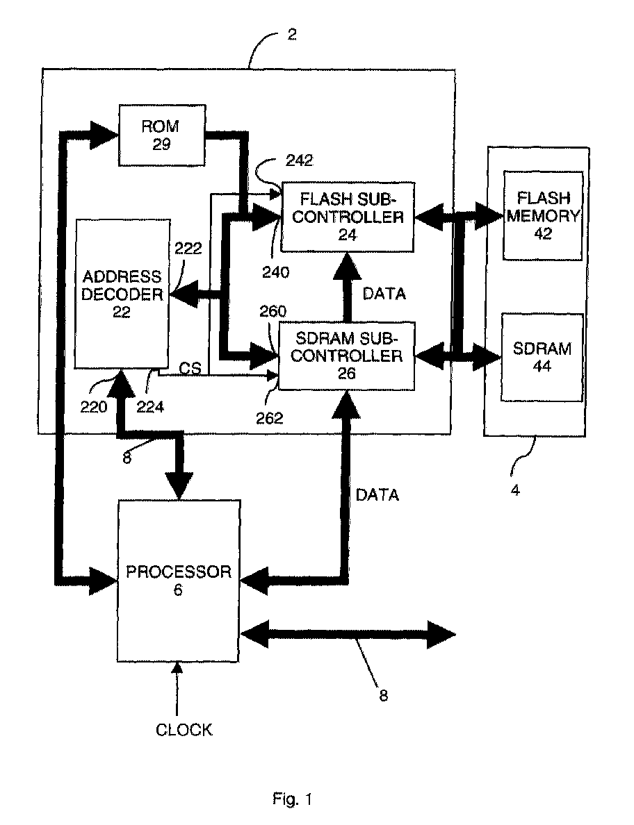
- a memory controller 2 in accordance with the invention comprises an address decoder 22 and at least a first sub-controller 24 and a second sub-controller 26.
- the memory controller 2 controls the transfer of data to and from a memory array 4 and operates under control of a microprocessor 6.
- the memory array 4 comprises at least a first type of memory 42 and a second type of memory 44.
- the first type of memory 42 is of a burst mode type, preferably a synchronous burst mode type e.g. the flash memory chip 28F160F3 from Intel Corporation.
- the second memory type is a Synchronous Dynamic Random Access Memory (SDRAM).
- SDRAM Synchronous Dynamic Random Access Memory
- Generally software is stored in the SDRAM whilst it is not running in the burst mode memory.
- the burst mode memory is used for the storage of code that is accessed frequently.
- Flash is the preferred type of burst mode memory since Flash memory is a non-volatile memory that can be erased in blocks. Flash is used to store application programs and user data and also provides "execute in place" functionality.
- Mask-ROM is another example of burst mode memory.
- the memory controller 2 operates under control of a microprocessor 6, which may be dedicated to this task. However the microprocessor 6 may also be a microprocessor shared between many resources of the device with which the memory controller operates.
- the processor 6 is connected to the memory controller 2 via the internal system bus 8 of the ASIC of the device with which the memory controller 2 is associated.
- the microprocessor executes code that may be stored in the microprocessor itself or in the memory array 4. Thus the microprocessor has to access the memory array 4 via the memory controller 2 to transfer data to and from the memory array.
- the address decoder has an input 220 for receiving a memory access request from the microprocessor 6.
- the memory access request includes the address of the memory array 4 to be accessed.
- the address decoder 22 has an output 222 for outputting the address to be accessed.
- the address decoder also has an output 224 for outputting a sub-controller select signal CS for selecting the sub-controller 24 or 26.
- the first sub-controller 24 has an input 240 for receiving the address to be accessed and an input 242 for receiving the sub-controller select signal CS. In response to an appropriate CS signal the first sub-controller 24 generates a plurality of memory signals for controlling the Flash memory 42.
- the second sub-controller 24 has an input 260 for receiving the address to be accessed and an input 262 for receiving the sub-controller select signal CS. In response to an appropriate CS signal the second sub-controller 24 generates a plurality of memory signals for controlling the SDRAM memory 44.
- outputs 222 and 224 are shown as dedicated outputs, a common data bus may be provided between the address decoder 22 and the sub-controllers 24, 26.
- a range of addresses is allocated to each type of memory in the memory array 4. For instance, say the total capacity of the memory array 4 is 2GB.
- the addresses 0 to 16MB are allocated to the Flash memory 42 and addresses above 16MB are allocated to the SDRAM 44. This information is stored in the address decoder 22.
- the address decoder 22 decodes and examines the address of the memory access request and selects the appropriate sub-controller 24, 26 on the basis of the address. If the address to be accessed is within the range of addresses allocated to the first type of memory 42, the address decoder outputs a sub-controller select signal CS1. If the address to be accessed is within the range of addresses allocated to the second type of memory 44, the address decoder outputs a sub-controller select signal CS2. The appropriate sub-controller then generates the appropriate memory access protocol signals.
- the sub-controller 24 In response to the sub-controller select signal CS1, the sub-controller 24 generates a plurality of memory interface signals for controlling the burst type memory 42.
- Figure 2 shows an example of the memory interface signals generated by the first sub-controller 24.
- the sub-controller 24 generates: a 22-bit address signal ADDR; a DATA signal that comprises at least one burst of 16 bits; and an address valid signal ADV. When the ADV signal is low, the address information is transmitted.
- the sub-controller 26 In response to the sub-controller select signal CS2, the sub-controller 26 generates a plurality of memory interface signals for controlling the SDRAM memory 44.
- Figure 3 shows an example of the memory interface signals generated by the second sub-controller 26.
- the sub-controller 26 generates: a 12 bit address signal ADDR that includes a column address COL and a row address ROW; a column address signal CAS and a row address signal RAS, which indicate when column or row data respectively is being transmitted; a DATA signal that comprises at least 16 bits; and a clock signal CLK.
- the ROW address may be transmitted before the COL address and that the CAS and RAS signals may be active high (as shown) or active low.
- the processor 6 may configure the parameters of the sub-controllers 24, 26.
- Examples of the sub-controller parameters that the processor may configure are the clock frequency of the memory bus, number of wait states, size of the memory type associated with the sub-controller etc.
- the parameters of the address decoder may also be configurable so that the address ranges allocated to each type of memory may be altered.
- Figure 4 shows the pin implementation of a memory controller according to a second embodiment of the invention.
- the memory controller is arranged to operate with three types of memory: Flash memory 42, first SDRAM 44 and second SDRAM 46.
- a first pin 201 outputs the first 14 bits of the address for the SDRAM memory 44 or 46 and the last 6 bits (bits 16-21) of the address for the Flash memory 42.
- Pin 202 outputs the 16 bit data for the SDRAM memory and the 16 bit data or the 16 MSB of the address for the Flash memory 42.
- Pin 203 outputs the chip select signal CS1 for the Flash memory 42.
- Pin 204 outputs the chip select signal CS2 for the SDRAM memory 44.
- Pin 205 outputs the chip select signal CS3 for the SDRAM memory 46.
- Pin 206 outputs a Clock Enable signal CKE1 for the Flash memory 42.
- Pin 207 outputs a CKE2 signal for the SDRAM memory 44.
- Pin 208 outputs a CKE3 signal for the SDRAM memory 46
- the memory controller may also include Read Only Memory (ROM) 29. This is used to store the code used by the device on start-up.
- ROM Read Only Memory
- the microprocessor When the microprocessor is reset (e.g. the device is switched on) the microprocessor 6 interrogates the ROM.
- Stored in the ROM is information regarding the type of memory to be accessed when the device is reset. For instance the ROM may include instructions that the memory controller should always access the Flash memory on reset.
- the Flash memory may store information regarding the address ranges to be used by the memory controller 2. This information is read by the microprocessor and stored in the address decoder 22 of the memory controller.
- the address information may either be hardwired into the address decoder 22 or this information may be downloaded from the boot ROM 29.
- the memory controller 2 or boot ROM 29 may be programmed with instructions as to how and from where to download this information.
- the method for accessing the first memory can be found from the BOOT ROM/hardwired logic of the memory controller, then the device will gain access to the first memory during boot up and by downloading information from the first memory it will gain access to other memories.
- the device may access this information via an external interface (such as RS232) during boot up from Boot ROM 29 or the hardwired logic of memory controller 2 and by using this interface it may download information needed for accessing memories.
- an external interface such as RS232
Abstract
A memory controller for controlling the transfer of data to and from a memory
array, wherein the memory array includes a first type of memory and a second
type of memory, the first type having a different signalling protocol from the
second type of memory, wherein the memory controller comprises:
Description
- This invention relates to a memory controller and in particular to a memory controller for controlling the transmission of data to and from a memory array comprising at least a first type and a second type of memory.
- An example of a known memory controller is described in US Patent No. 5721860.
- In accordance with the invention there is provided a memory controller for controlling the transfer of data to and from a memory array, wherein the memory array includes a first type of memory and a second type of memory, the first type having a different signalling protocol from the second type of memory, wherein the memory controller comprises:
- an address decoder having an input for receiving a memory access request, said memory access request including the address of the memory array to be accessed, and an output for outputting the address of the memory array to be accessed;
- a first sub-controller for generating a plurality of memory interface signals for controlling the first type of memory, said first sub-controller being operated in response to addresses within a first range of addresses output by the address decoder; and
- a second sub-controller for generating a plurality of memory interface signals for controlling the second type of memory, said second sub-controller being operated in response to addresses within a second, non-overlapping range of addresses output by the address decoder.
-
- A user can therefore define the areas of memory to be dedicated to a particular type of memory and add these types of memory as and when required. Such a memory controller therefore provides a user with the flexibility to connect different types of memory to a device via a single bus and to store information as to the address range to be allocated to a particular type of memory.
- The memory controller of the invention may be used in a variety of electronic devices such as portable radio telecommunications devices (e.g. telephones and communicators).
- Preferably the first type of memory is a burst mode type of memory, in particular flash memory. The memory may be synchronous or asynchronous. The addressing protocol may include multiplexed address and data.
- Preferably parameters of the memory controller are configurable e.g. the first and second range of addresses may be configurable.
- In accordance with the invention there is also provided a method of controlling the transfer of data to and from a memory array in an electronic device, wherein the memory array includes a first type of memory and a second type of memory, the first type having a different signalling protocol from the second type of memory, wherein the method comprises:
- receiving a memory access request, said memory access request including the address of the memory array to be accessed, and outputting the address of the memory array to be accessed;
- in response to addresses within a first range of addresses generating a plurality of memory interface signals for controlling the first type of memory; and
- in response to addresses within a second, non-overlapping range of addresses generating a plurality of memory interface signals for controlling the second type of memory.
-
- The invention will now be described, by way of example only, with reference to the accompanying drawings, in which:
- Figure 1 shows the components of a memory controller in accordance with the invention;
- Figure 2 shows an example of the memory interface signals generated by a first sub-controller;
- Figure 3 shows an example of the memory interface signals generated by a second sub-controller; and
- Figure 4 shows an example of an implementation of a memory controller according to the invention.
-
- As shown in Figure 1 a
memory controller 2 in accordance with the invention comprises anaddress decoder 22 and at least afirst sub-controller 24 and asecond sub-controller 26. Thememory controller 2 controls the transfer of data to and from amemory array 4 and operates under control of amicroprocessor 6. - The
memory array 4 comprises at least a first type ofmemory 42 and a second type ofmemory 44. The first type ofmemory 42 is of a burst mode type, preferably a synchronous burst mode type e.g. the flash memory chip 28F160F3 from Intel Corporation. The second memory type is a Synchronous Dynamic Random Access Memory (SDRAM). Generally software is stored in the SDRAM whilst it is not running in the burst mode memory. Generally the burst mode memory is used for the storage of code that is accessed frequently. Flash is the preferred type of burst mode memory since Flash memory is a non-volatile memory that can be erased in blocks. Flash is used to store application programs and user data and also provides "execute in place" functionality. Mask-ROM is another example of burst mode memory. - The
memory controller 2 operates under control of amicroprocessor 6, which may be dedicated to this task. However themicroprocessor 6 may also be a microprocessor shared between many resources of the device with which the memory controller operates. Theprocessor 6 is connected to thememory controller 2 via theinternal system bus 8 of the ASIC of the device with which thememory controller 2 is associated. - The microprocessor executes code that may be stored in the microprocessor itself or in the
memory array 4. Thus the microprocessor has to access thememory array 4 via thememory controller 2 to transfer data to and from the memory array. - The address decoder has an
input 220 for receiving a memory access request from themicroprocessor 6. The memory access request includes the address of thememory array 4 to be accessed. Theaddress decoder 22 has anoutput 222 for outputting the address to be accessed. The address decoder also has anoutput 224 for outputting a sub-controller select signal CS for selecting thesub-controller - The
first sub-controller 24 has aninput 240 for receiving the address to be accessed and aninput 242 for receiving the sub-controller select signal CS. In response to an appropriate CS signal thefirst sub-controller 24 generates a plurality of memory signals for controlling the Flashmemory 42. - The
second sub-controller 24 has aninput 260 for receiving the address to be accessed and aninput 262 for receiving the sub-controller select signal CS. In response to an appropriate CS signal thesecond sub-controller 24 generates a plurality of memory signals for controlling theSDRAM memory 44. - Although the
outputs address decoder 22 and thesub-controllers - The operation of the
address decoder 22 will now be described in more detail. A range of addresses is allocated to each type of memory in thememory array 4. For instance, say the total capacity of thememory array 4 is 2GB. - The addresses 0 to 16MB are allocated to the
Flash memory 42 and addresses above 16MB are allocated to theSDRAM 44. This information is stored in theaddress decoder 22. - In use, when the
processor 6 accesses the memory, for example to fetch an instruction from the Flashmemory 42, the address is first passed to thememory controller 2 through theinternal bus 8. When the address decoder receives a memory access request from themicroprocessor 6, theaddress decoder 22 decodes and examines the address of the memory access request and selects theappropriate sub-controller memory 42, the address decoder outputs a sub-controller select signal CS1. If the address to be accessed is within the range of addresses allocated to the second type ofmemory 44, the address decoder outputs a sub-controller select signal CS2. The appropriate sub-controller then generates the appropriate memory access protocol signals. - In response to the sub-controller select signal CS1, the
sub-controller 24 generates a plurality of memory interface signals for controlling theburst type memory 42. Figure 2 shows an example of the memory interface signals generated by thefirst sub-controller 24. Thesub-controller 24 generates: a 22-bit address signal ADDR; a DATA signal that comprises at least one burst of 16 bits; and an address valid signal ADV. When the ADV signal is low, the address information is transmitted. - In response to the sub-controller select signal CS2, the
sub-controller 26 generates a plurality of memory interface signals for controlling theSDRAM memory 44. Figure 3 shows an example of the memory interface signals generated by thesecond sub-controller 26. Thesub-controller 26 generates: a 12 bit address signal ADDR that includes a column address COL and a row address ROW; a column address signal CAS and a row address signal RAS, which indicate when column or row data respectively is being transmitted; a DATA signal that comprises at least 16 bits; and a clock signal CLK. It will be clear to a person skilled in the art that the ROW address may be transmitted before the COL address and that the CAS and RAS signals may be active high (as shown) or active low. - The
processor 6 may configure the parameters of thesub-controllers - Figure 4 shows the pin implementation of a memory controller according to a second embodiment of the invention. In this embodiment, the memory controller is arranged to operate with three types of memory:
Flash memory 42,first SDRAM 44 andsecond SDRAM 46. Afirst pin 201 outputs the first 14 bits of the address for theSDRAM memory Flash memory 42. Pin 202 outputs the 16 bit data for the SDRAM memory and the 16 bit data or the 16 MSB of the address for theFlash memory 42. Pin 203 outputs the chip select signal CS1 for theFlash memory 42. Pin 204 outputs the chip select signal CS2 for theSDRAM memory 44. Pin 205 outputs the chip select signal CS3 for theSDRAM memory 46. Pin 206 outputs a Clock Enable signal CKE1 for theFlash memory 42. Pin 207 outputs a CKE2 signal for theSDRAM memory 44. Pin 208 outputs a CKE3 signal for theSDRAM memory 46. - The memory controller may also include Read Only Memory (ROM) 29. This is used to store the code used by the device on start-up. When the microprocessor is reset (e.g. the device is switched on) the
microprocessor 6 interrogates the ROM. Stored in the ROM is information regarding the type of memory to be accessed when the device is reset. For instance the ROM may include instructions that the memory controller should always access the Flash memory on reset. The Flash memory may store information regarding the address ranges to be used by thememory controller 2. This information is read by the microprocessor and stored in theaddress decoder 22 of the memory controller. - The address information (i.e. ranges and type of memory) may either be hardwired into the
address decoder 22 or this information may be downloaded from the boot ROM 29. Alternatively thememory controller 2 or boot ROM 29 may be programmed with instructions as to how and from where to download this information. Thus if the method for accessing the first memory can be found from the BOOT ROM/hardwired logic of the memory controller, then the device will gain access to the first memory during boot up and by downloading information from the first memory it will gain access to other memories. Altematively the device may access this information via an external interface (such as RS232) during boot up from Boot ROM 29 or the hardwired logic ofmemory controller 2 and by using this interface it may download information needed for accessing memories. - This way of downloading the information enables an straightforward way to change the memory components without any need to change the ASIC.
Claims (12)
- A memory controller for controlling the transfer of data to and from a memory array, wherein the memory array includes a first type of memory and a second type of memory, the first type having a different signalling protocol from the second type of memory, wherein the memory controller comprises:an address decoder having an input for receiving a memory access request, said memory access request including the address of the memory array to be accessed, and an output for outputting the address of the memory array to be accessed;a first sub-controller for generating a plurality of memory interface signals for controlling the first type of memory, said first sub-controller being operated in response to addresses within a first range of addresses output by the address decoder; anda second sub-controller for generating a plurality of memory interface signals for controlling the second type of memory, said second sub-controller being operated in response to addresses within a second, non-overlapping range of addresses output by the address decoder.
- A memory controller according to claim 1 wherein the first type of memory is a burst mode type of memory.
- A memory controller according to claim 2 wherein the first type of memory is flash memory.
- A memory controller according to claim 1, 2 or 3 wherein the first type of memory is MROM.
- A memory controller according to any preceding claim wherein the second type of memory is Synchronous Dynamic Random Access Memory.
- A memory controller according to any preceding claim 1, 2 or 3 wherein parameters of the memory controller are configurable.
- A memory controller according to claim 6 wherein the first and second range of addresses are configurable.
- An electronic device including a memory controller as claimed in any of claims 1 to 7.
- An electronic telecommunications device including a memory controller as claimed in any of claims 1 to 7.
- A method of controlling the transfer of data to and from a memory array in an electronic device, wherein the memory array includes a first type of memory and a second type of memory, the first type having a different signalling protocol from the second type of memory, wherein the method comprises:receiving a memory access request, said memory access request including the address of the memory array to be accessed, and outputting the address of the memory array to be accessed;in response to addresses within a first range of addresses generating a plurality of memory interface signals for controlling the first type of memory; andin response to addresses within a second, non-overlapping range of addresses generating a plurality of memory interface signals for controlling the second type of memory.
- A memory controller substantially as described herein with reference to the accompanying drawings.
- A method of controlling memory accesses substantially as described herein with reference to the accompanying drawings.
Applications Claiming Priority (2)
| Application Number | Priority Date | Filing Date | Title |
|---|---|---|---|
| GB9930413A GB2357602A (en) | 1999-12-22 | 1999-12-22 | Memory controller for a memory array comprising different memory types |
| GB9930413 | 1999-12-22 |
Publications (1)
| Publication Number | Publication Date |
|---|---|
| EP1132819A2 true EP1132819A2 (en) | 2001-09-12 |
Family
ID=10866881
Family Applications (1)
| Application Number | Title | Priority Date | Filing Date |
|---|---|---|---|
| EP00311268A Withdrawn EP1132819A2 (en) | 1999-12-22 | 2000-12-15 | Memory controller |
Country Status (3)
| Country | Link |
|---|---|
| US (1) | US6563739B2 (en) |
| EP (1) | EP1132819A2 (en) |
| GB (1) | GB2357602A (en) |
Cited By (3)
| Publication number | Priority date | Publication date | Assignee | Title |
|---|---|---|---|---|
| WO2003021600A3 (en) * | 2001-08-29 | 2003-10-23 | Analog Devices Inc | Methods and apparatus utilizing flash burst mode to improve processor performance |
| WO2004051484A2 (en) * | 2002-12-05 | 2004-06-17 | Nokia Corporation | Device and method for operating memory components |
| WO2012003275A1 (en) * | 2010-07-01 | 2012-01-05 | Qualcomm Incorporated | Parallel use of integrated non-volatile memory and main volatile memory within a mobile device |
Families Citing this family (45)
| Publication number | Priority date | Publication date | Assignee | Title |
|---|---|---|---|---|
| JP2001249891A (en) * | 2000-03-03 | 2001-09-14 | Sony Computer Entertainment Inc | Entertainment device |
| WO2002048860A2 (en) * | 2000-12-14 | 2002-06-20 | Psion Digital Limited | Synchronous memory controller |
| JP4060235B2 (en) | 2003-05-22 | 2008-03-12 | 株式会社日立製作所 | Disk array device and disk array device control method |
| JP2004348464A (en) * | 2003-05-22 | 2004-12-09 | Hitachi Ltd | Storage device and communication signal shaping circuit |
| JP4156499B2 (en) * | 2003-11-28 | 2008-09-24 | 株式会社日立製作所 | Disk array device |
| JP4497918B2 (en) * | 2003-12-25 | 2010-07-07 | 株式会社日立製作所 | Storage system |
| JP4634049B2 (en) | 2004-02-04 | 2011-02-16 | 株式会社日立製作所 | Error notification control in disk array system |
| US9171585B2 (en) | 2005-06-24 | 2015-10-27 | Google Inc. | Configurable memory circuit system and method |
| US8386722B1 (en) | 2008-06-23 | 2013-02-26 | Google Inc. | Stacked DIMM memory interface |
| US10013371B2 (en) | 2005-06-24 | 2018-07-03 | Google Llc | Configurable memory circuit system and method |
| US8397013B1 (en) * | 2006-10-05 | 2013-03-12 | Google Inc. | Hybrid memory module |
| US8077535B2 (en) | 2006-07-31 | 2011-12-13 | Google Inc. | Memory refresh apparatus and method |
| US8111566B1 (en) | 2007-11-16 | 2012-02-07 | Google, Inc. | Optimal channel design for memory devices for providing a high-speed memory interface |
| US7386656B2 (en) | 2006-07-31 | 2008-06-10 | Metaram, Inc. | Interface circuit system and method for performing power management operations in conjunction with only a portion of a memory circuit |
| US8090897B2 (en) | 2006-07-31 | 2012-01-03 | Google Inc. | System and method for simulating an aspect of a memory circuit |
| US20080028136A1 (en) | 2006-07-31 | 2008-01-31 | Schakel Keith R | Method and apparatus for refresh management of memory modules |
| US8796830B1 (en) | 2006-09-01 | 2014-08-05 | Google Inc. | Stackable low-profile lead frame package |
| US9507739B2 (en) | 2005-06-24 | 2016-11-29 | Google Inc. | Configurable memory circuit system and method |
| US8327104B2 (en) | 2006-07-31 | 2012-12-04 | Google Inc. | Adjusting the timing of signals associated with a memory system |
| US9542352B2 (en) | 2006-02-09 | 2017-01-10 | Google Inc. | System and method for reducing command scheduling constraints of memory circuits |
| US8060774B2 (en) | 2005-06-24 | 2011-11-15 | Google Inc. | Memory systems and memory modules |
| US8359187B2 (en) | 2005-06-24 | 2013-01-22 | Google Inc. | Simulating a different number of memory circuit devices |
| US8055833B2 (en) | 2006-10-05 | 2011-11-08 | Google Inc. | System and method for increasing capacity, performance, and flexibility of flash storage |
| US8081474B1 (en) | 2007-12-18 | 2011-12-20 | Google Inc. | Embossed heat spreader |
| US7609567B2 (en) | 2005-06-24 | 2009-10-27 | Metaram, Inc. | System and method for simulating an aspect of a memory circuit |
| US8244971B2 (en) | 2006-07-31 | 2012-08-14 | Google Inc. | Memory circuit system and method |
| US20080082763A1 (en) | 2006-10-02 | 2008-04-03 | Metaram, Inc. | Apparatus and method for power management of memory circuits by a system or component thereof |
| US8130560B1 (en) | 2006-11-13 | 2012-03-06 | Google Inc. | Multi-rank partial width memory modules |
| US8335894B1 (en) | 2008-07-25 | 2012-12-18 | Google Inc. | Configurable memory system with interface circuit |
| US8041881B2 (en) | 2006-07-31 | 2011-10-18 | Google Inc. | Memory device with emulated characteristics |
| US8089795B2 (en) | 2006-02-09 | 2012-01-03 | Google Inc. | Memory module with memory stack and interface with enhanced capabilities |
| US8438328B2 (en) * | 2008-02-21 | 2013-05-07 | Google Inc. | Emulation of abstracted DIMMs using abstracted DRAMs |
| DE112006002300B4 (en) | 2005-09-02 | 2013-12-19 | Google, Inc. | Device for stacking DRAMs |
| US9632929B2 (en) | 2006-02-09 | 2017-04-25 | Google Inc. | Translating an address associated with a command communicated between a system and memory circuits |
| ITRM20060139A1 (en) | 2006-03-13 | 2007-09-14 | Micron Technology Inc | DISTRIBUTED MEMORY DEVICE CONTROL UNIT SYSTEM |
| US7499339B2 (en) * | 2006-07-19 | 2009-03-03 | Sandisk Corporation | High-performance flash memory data transfer |
| US7499369B2 (en) * | 2006-07-19 | 2009-03-03 | Sandisk Corporation | Method of high-performance flash memory data transfer |
| US7525855B2 (en) * | 2006-04-24 | 2009-04-28 | Sandisk Corporation | Method of high-performance flash memory data transfer |
| CN101702947B (en) * | 2007-04-12 | 2017-02-15 | 拉姆伯斯公司 | memory system with point-to-point request interconnect, memory controller and method |
| US8347005B2 (en) * | 2007-07-31 | 2013-01-01 | Hewlett-Packard Development Company, L.P. | Memory controller with multi-protocol interface |
| US8080874B1 (en) | 2007-09-14 | 2011-12-20 | Google Inc. | Providing additional space between an integrated circuit and a circuit board for positioning a component therebetween |
| WO2010144624A1 (en) | 2009-06-09 | 2010-12-16 | Google Inc. | Programming of dimm termination resistance values |
| US9323457B2 (en) | 2013-12-09 | 2016-04-26 | Xilinx, Inc. | Memory arrangement for implementation of high-throughput key-value stores |
| US9711194B2 (en) * | 2015-01-28 | 2017-07-18 | Xilinx, Inc. | Circuits for and methods of controlling the operation of a hybrid memory system |
| US20230236742A1 (en) * | 2022-01-22 | 2023-07-27 | Micron Technology, Inc. | NONVOLATILE MEMORY EXPRESS (NVMe) OVER COMPUTE EXPRESS LINK (CXL) |
Family Cites Families (10)
| Publication number | Priority date | Publication date | Assignee | Title |
|---|---|---|---|---|
| US4281392A (en) * | 1979-05-01 | 1981-07-28 | Allen-Bradley Company | Memory circuit for programmable machines |
| US5040153A (en) * | 1987-10-23 | 1991-08-13 | Chips And Technologies, Incorporated | Addressing multiple types of memory devices |
| US5200600A (en) * | 1988-08-29 | 1993-04-06 | Hitachi Maxell, Ltd. | IC card and method for writing information therein |
| AU2918092A (en) * | 1991-11-01 | 1993-06-07 | Keming W. Yeh | Portable device having data storage capability for transferring data between a portable computer and a desktop computer |
| TW231343B (en) * | 1992-03-17 | 1994-10-01 | Hitachi Seisakusyo Kk | |
| US5848247A (en) * | 1994-09-13 | 1998-12-08 | Hitachi, Ltd. | Microprocessor having PC card interface |
| US5838603A (en) * | 1994-10-11 | 1998-11-17 | Matsushita Electric Industrial Co., Ltd. | Semiconductor device and method for fabricating the same, memory core chip and memory peripheral circuit chip |
| DE59610672D1 (en) * | 1995-12-29 | 2003-09-25 | Siemens Ag | Method and arrangement for converting memory addresses into memory control signals |
| FR2778258A1 (en) * | 1998-04-29 | 1999-11-05 | Texas Instruments France | Memory traffic access controller |
| US6179205B1 (en) * | 1998-03-05 | 2001-01-30 | Visa International Service Association | System and method for locking and unlocking and application in a smart card |
-
1999
- 1999-12-22 GB GB9930413A patent/GB2357602A/en not_active Withdrawn
-
2000
- 2000-12-15 EP EP00311268A patent/EP1132819A2/en not_active Withdrawn
- 2000-12-21 US US09/740,802 patent/US6563739B2/en not_active Expired - Lifetime
Cited By (13)
| Publication number | Priority date | Publication date | Assignee | Title |
|---|---|---|---|---|
| WO2003021600A3 (en) * | 2001-08-29 | 2003-10-23 | Analog Devices Inc | Methods and apparatus utilizing flash burst mode to improve processor performance |
| US7007132B2 (en) | 2001-08-29 | 2006-02-28 | Analog Devices, Inc. | Methods and apparatus for utilizing flash burst mode to improve processor performance |
| WO2004051484A2 (en) * | 2002-12-05 | 2004-06-17 | Nokia Corporation | Device and method for operating memory components |
| WO2004051484A3 (en) * | 2002-12-05 | 2005-12-01 | Nokia Corp | Device and method for operating memory components |
| US7010632B2 (en) | 2002-12-05 | 2006-03-07 | Nokia Corporation | Operating memory components |
| CN102959525A (en) * | 2010-07-01 | 2013-03-06 | 高通股份有限公司 | Parallel use of integrated non-volatile memory and main volatile memory within mobile device |
| WO2012003275A1 (en) * | 2010-07-01 | 2012-01-05 | Qualcomm Incorporated | Parallel use of integrated non-volatile memory and main volatile memory within a mobile device |
| JP2013534015A (en) * | 2010-07-01 | 2013-08-29 | クアルコム,インコーポレイテッド | Parallel use of embedded non-volatile memory and main volatile memory in mobile devices |
| JP2014194794A (en) * | 2010-07-01 | 2014-10-09 | Qualcomm Inc | Parallel use of integrated non-volatile memory and main volatile memory within mobile device |
| KR101466599B1 (en) * | 2010-07-01 | 2014-11-28 | 퀄컴 인코포레이티드 | Parallel use of integrated non-volatile memory and main volatile memory within a mobile device |
| JP2016076251A (en) * | 2010-07-01 | 2016-05-12 | クアルコム,インコーポレイテッド | Parallel use of integrated non-volatile memory and main volatile memory within mobile device |
| CN102959525B (en) * | 2010-07-01 | 2016-07-06 | 高通股份有限公司 | Integrating nonvolatile memory in mobile device uses with the parallel of main volatile memory |
| US10360143B2 (en) | 2010-07-01 | 2019-07-23 | Qualcomm Incorporated | Parallel use of integrated non-volatile memory and main volatile memory within a mobile device |
Also Published As
| Publication number | Publication date |
|---|---|
| US20010019509A1 (en) | 2001-09-06 |
| US6563739B2 (en) | 2003-05-13 |
| GB2357602A (en) | 2001-06-27 |
| GB9930413D0 (en) | 2000-02-16 |
Similar Documents
| Publication | Publication Date | Title |
|---|---|---|
| EP1132819A2 (en) | Memory controller | |
| JP5290516B2 (en) | Memory device, system having memory device, and method of operating embedded device | |
| EP0818731B1 (en) | Memory board, memory access method and memory access device | |
| US7930530B2 (en) | Multi-processor system that reads one of a plurality of boot codes via memory interface buffer in response to requesting processor | |
| KR100262030B1 (en) | Memory system and semiconductor memory device used therefor | |
| US7398383B2 (en) | Method and system for using internal FIFO RAM to improve system boot times | |
| KR100679758B1 (en) | Data processor integrated circuit with a memory interface unit with programmable strobes to select different memory devices | |
| US6584528B1 (en) | Microprocessor allocating no wait storage of variable capacity to plurality of resources, and memory device therefor | |
| US20070283139A1 (en) | Information processing apparatus and control method used thereby | |
| US6735643B2 (en) | Electronic card with dynamic memory allocation management | |
| US6725346B1 (en) | Method and apparatus for overlaying memory in a data processing system | |
| US5961611A (en) | Automatic option setting circuit | |
| US5781492A (en) | System and method for mapping memory to DRAM after system boot from non-volatile memory | |
| US5974519A (en) | Address re-designate circuit for microcontroller | |
| KR20040045446A (en) | Interfacing processors with external memory supporting burst mode | |
| GB2304209A (en) | Starting up a processor system | |
| JP4121373B2 (en) | Harvard architecture microprocessor with linear addressable space. | |
| KR100329768B1 (en) | Memory addressing device for micro-controller unit | |
| KR100321840B1 (en) | Address re-mapping for memory module using presence detect data | |
| JP2001209763A (en) | One-chip microcomputer and ic card incorporated with the same | |
| JPH04324566A (en) | Method for controlling memory map switching of multiprocessor system | |
| KR20010009941A (en) | booting apparatus and method for data processing System | |
| JPH11110984A (en) | Access method for re-writable rom | |
| JP2001155006A (en) | Bus control circuit and microcomputer system using the same | |
| JP2000207622A (en) | Initialization processing device for vending machine |
Legal Events
| Date | Code | Title | Description |
|---|---|---|---|
| PUAI | Public reference made under article 153(3) epc to a published international application that has entered the european phase |
Free format text: ORIGINAL CODE: 0009012 |
|
| AK | Designated contracting states |
Kind code of ref document: A2 Designated state(s): AT BE CH CY DE DK ES FI FR GB GR IE IT LI LU MC NL PT SE TR |
|
| AX | Request for extension of the european patent |
Free format text: AL;LT;LV;MK;RO;SI |
|
| RAP1 | Party data changed (applicant data changed or rights of an application transferred) |
Owner name: NOKIA CORPORATION |
|
| STAA | Information on the status of an ep patent application or granted ep patent |
Free format text: STATUS: THE APPLICATION HAS BEEN WITHDRAWN |
|
| 18W | Application withdrawn |
Effective date: 20030106 |