EP1136235A1 - Method and apparatus of correcting superfluous curing thickness of optical modeling product - Google Patents
Method and apparatus of correcting superfluous curing thickness of optical modeling product Download PDFInfo
- Publication number
- EP1136235A1 EP1136235A1 EP01112022A EP01112022A EP1136235A1 EP 1136235 A1 EP1136235 A1 EP 1136235A1 EP 01112022 A EP01112022 A EP 01112022A EP 01112022 A EP01112022 A EP 01112022A EP 1136235 A1 EP1136235 A1 EP 1136235A1
- Authority
- EP
- European Patent Office
- Prior art keywords
- patch
- nodes
- overhang portion
- surface shape
- curing
- Prior art date
- Legal status (The legal status is an assumption and is not a legal conclusion. Google has not performed a legal analysis and makes no representation as to the accuracy of the status listed.)
- Granted
Links
Images


Classifications
-
- B—PERFORMING OPERATIONS; TRANSPORTING
- B29—WORKING OF PLASTICS; WORKING OF SUBSTANCES IN A PLASTIC STATE IN GENERAL
- B29C—SHAPING OR JOINING OF PLASTICS; SHAPING OF MATERIAL IN A PLASTIC STATE, NOT OTHERWISE PROVIDED FOR; AFTER-TREATMENT OF THE SHAPED PRODUCTS, e.g. REPAIRING
- B29C64/00—Additive manufacturing, i.e. manufacturing of three-dimensional [3D] objects by additive deposition, additive agglomeration or additive layering, e.g. by 3D printing, stereolithography or selective laser sintering
- B29C64/10—Processes of additive manufacturing
- B29C64/106—Processes of additive manufacturing using only liquids or viscous materials, e.g. depositing a continuous bead of viscous material
- B29C64/124—Processes of additive manufacturing using only liquids or viscous materials, e.g. depositing a continuous bead of viscous material using layers of liquid which are selectively solidified
- B29C64/129—Processes of additive manufacturing using only liquids or viscous materials, e.g. depositing a continuous bead of viscous material using layers of liquid which are selectively solidified characterised by the energy source therefor, e.g. by global irradiation combined with a mask
- B29C64/135—Processes of additive manufacturing using only liquids or viscous materials, e.g. depositing a continuous bead of viscous material using layers of liquid which are selectively solidified characterised by the energy source therefor, e.g. by global irradiation combined with a mask the energy source being concentrated, e.g. scanning lasers or focused light sources
-
- B—PERFORMING OPERATIONS; TRANSPORTING
- B33—ADDITIVE MANUFACTURING TECHNOLOGY
- B33Y—ADDITIVE MANUFACTURING, i.e. MANUFACTURING OF THREE-DIMENSIONAL [3-D] OBJECTS BY ADDITIVE DEPOSITION, ADDITIVE AGGLOMERATION OR ADDITIVE LAYERING, e.g. BY 3-D PRINTING, STEREOLITHOGRAPHY OR SELECTIVE LASER SINTERING
- B33Y50/00—Data acquisition or data processing for additive manufacturing
-
- B—PERFORMING OPERATIONS; TRANSPORTING
- B29—WORKING OF PLASTICS; WORKING OF SUBSTANCES IN A PLASTIC STATE IN GENERAL
- B29C—SHAPING OR JOINING OF PLASTICS; SHAPING OF MATERIAL IN A PLASTIC STATE, NOT OTHERWISE PROVIDED FOR; AFTER-TREATMENT OF THE SHAPED PRODUCTS, e.g. REPAIRING
- B29C35/00—Heating, cooling or curing, e.g. crosslinking or vulcanising; Apparatus therefor
- B29C35/02—Heating or curing, e.g. crosslinking or vulcanizing during moulding, e.g. in a mould
- B29C35/08—Heating or curing, e.g. crosslinking or vulcanizing during moulding, e.g. in a mould by wave energy or particle radiation
- B29C35/0805—Heating or curing, e.g. crosslinking or vulcanizing during moulding, e.g. in a mould by wave energy or particle radiation using electromagnetic radiation
- B29C2035/0838—Heating or curing, e.g. crosslinking or vulcanizing during moulding, e.g. in a mould by wave energy or particle radiation using electromagnetic radiation using laser
-
- B—PERFORMING OPERATIONS; TRANSPORTING
- B29—WORKING OF PLASTICS; WORKING OF SUBSTANCES IN A PLASTIC STATE IN GENERAL
- B29C—SHAPING OR JOINING OF PLASTICS; SHAPING OF MATERIAL IN A PLASTIC STATE, NOT OTHERWISE PROVIDED FOR; AFTER-TREATMENT OF THE SHAPED PRODUCTS, e.g. REPAIRING
- B29C37/00—Component parts, details, accessories or auxiliary operations, not covered by group B29C33/00 or B29C35/00
- B29C2037/90—Measuring, controlling or regulating
- B29C2037/903—Measuring, controlling or regulating by means of a computer
-
- B—PERFORMING OPERATIONS; TRANSPORTING
- B29—WORKING OF PLASTICS; WORKING OF SUBSTANCES IN A PLASTIC STATE IN GENERAL
- B29C—SHAPING OR JOINING OF PLASTICS; SHAPING OF MATERIAL IN A PLASTIC STATE, NOT OTHERWISE PROVIDED FOR; AFTER-TREATMENT OF THE SHAPED PRODUCTS, e.g. REPAIRING
- B29C37/00—Component parts, details, accessories or auxiliary operations, not covered by group B29C33/00 or B29C35/00
- B29C37/005—Compensating volume or shape change during moulding, in general
Definitions
- a superfluous curing thickness ⁇ at the bottom of an overhang portion is determined pursuant to the following equation (1), and the superfluous curing thickness ⁇ is precedently removed from a design value in a three-dimensional shape model and converted into contour line data.
- the dimensional difference inherent to optical modeling technique can be corrected automatically on surface shape data and the dimensional accuracy of an optical modeling product can be improved by performing modeling on the basis of surface shape data after correction. Further, since the aforementioned correction processing can be effected automatically, efficiency of the dimensional difference correction can be improved. In addition, such a secondary working step as shaving can be omitted.
- the modeling product bottom and overhang portion bottom can be detected automatically, the dimensional difference can be corrected efficiently on surface shape data and an optical modeling product of high dimensional accuracy can be obtained by performing modeling on the basis of the data.
- Fig. 12 shows the relation between lamination thickness and dimensional difference.
- the data is indicative of results obtained with the bottom of a horizontal overhang portion.
Abstract
Description
- The present invention relates to optical modeling method and apparatus of preparing a cubic resin model by curing ultraviolet-ray curable resin under irradiation of a laser beam and more particularly, to method and apparatus for providing an optical modeling product of high dimensional accuracy by correcting a superfluous curing thickness due to a transmitting laser beam.
- Conventionally, in connection with optical modeling method and apparatus, a method has been known in which three-dimensional shape model data is converted into contour line data and sectional shapes at respective contour lines are sequentially laminated to prepare a cubic model as described in "Optical Modeling Method" by Maruya et al, Nikkan Kogyo Shinbunsha.
- Measures for improving accuracy are described in Japanese Patent Publication Nos. 4-79825, 4-79827, 5-33900 and 5-33901.
- Also, "RP&M·SLA Special Seminar", sponsored by Japanese 3D System, October 29-30, '92 describes that when a resin layer is subjected to laser irradiation by scanning a laser beam once or by intersecting laser beams, a curing depth at a laser beam intersecting portion is about 1.7 times as large as a curing depth at a scanned portion.
- The aforementioned prior arts have failed to take into consideration correction of a superfluous curing thickness due to a transmitting laser beam at the bottom of an overhang portion. Consequently, at the bottom of that portion, fresh resin is cured by a transmitting laser beam and the thickness exceeds a design value, raising a problem that the dimensional accuracy is degraded.
- Further, in order to match the dimension of a modeling product to a design value, a secondary working step such as shaving is needed but it is sometimes impossible for a narrow gap to be shaved and correction of a dimensional difference is needed.
- A method of modifying the design dimension in three-dimensional CAD is also available as a method of correcting the dimensional difference but the dimensional modification in CAD is not easy and is time-consuming.
- An object of the present invention is to solve the problems as above and to provide a method of automatically detecting the bottom of a modeling product or the bottom of an overhang portion and automatically correcting a dimensional difference inherent to (stereolithography).
- To accomplish the above object, the dimensional difference is automatically corrected on surface shape data through a method in which vertex of polygonal patches constituting the surface shape data are replaced with nodes and nodes constituting a polygonal patch lying at the bottom of an overhang portion are moved to change the shape and position of that polygonal patch, and modeling is carried out based on those data.
- To accomplish the above object, a superfluous curing thickness α at the bottom of an overhang portion is determined pursuant to the following equation (1), and the superfluous curing thickness α is precedently removed from a design value in a three-dimensional shape model and converted into contour line data.
- Given that the number of laminated layers of modeling of an overhang portion is N, lamination pitch is P, light absorption coefficient of resin is k, wavelength of curing beam is λ and the ratio of critical energy of resin curing to irradiation energy of a curing beam is Eo, a superfluous curing thickness α is determined for pre-correction of superfluous curing as below:
- C=(1-BN)/(1-B)
- B=EXP(-kP/λ).
-
- By removing and adding the superfluous curing thickness α determined form the above equation (1) from and to contour line data, an optical modeling product of high dimensional accuracy can be obtained.
- How to determine the superfluous curing thickness α will be described with reference to Fig. 5, Fig. 11 (a) and Fig. 11(b). Given that lamination pitch is P, depth to the top of a first curing layer is D, the number of laminated layers is N and light absorption coefficient of resin is k, transmitting beam energy En(D,N) at the depth D upon lamination of N layers is En(D,N)=EXP(-k(D+(N-1)P)/λ). As the lamination proceeds, a transmitting beam is irradiated many times on a lower portion of the first layer and accumulative energy Etotal (D,N) thereat is Etotal(D,N)=EXP(-kD/λ)
Accordingly, because of D=-λ/k(ln(Etotal(D,N)-ln(C)) being the depth to the top of the first layer and given that Etotal (D,N) is also critical curing power (ratio to irradiation power), the superfluous curing thickness α when N layers are laminated is α=D-P(n-1). - Further, to accomplish the above object, the direction of a normal vector of a patch plane of a polygonal patch constituting surface shape data is examined to decide whether an overhang exists, vertex constituting a patch are replaced with nodes so as to be put in order, the nodes are discriminated as to whether to be nodes constituting a polygonal patch lying at the bottom of an overhang portion, and when the nodes constitute the polygonal patch lying at the bottom of the overhang portion, these nodes are moved by a moving amount determined pursuant to a predetermined rule in accordance with an inclination of the patch plane to change the shape and position of the polygonal patch. At that time, when nodes are in common to a plurality of patches, the direction of a normal vector of a patch plane to be moved by a maximum of moving amounts determined by inclinations of respective patch planes is examined in order to know which direction that patch plane faces. If a Z axis component of the normal vector is negative, the patch plane faces downwards on the Z axis. Namely, when the Z axis direction is taken in the vertical direction, that patch is so discriminated as to lie at the overhang portion bottom. When vertexes constituting the patch are merely moved for correction in compliance with results of decision of the patch direction (normal vector), vertexes in common to a plurality of patches are sometimes moved by different amounts and the shape is disturbed. Therefore, vertexes of a polygonal patch are put in order in the form of nodes, these nodes are discriminated as to whether to lie at the overhang bottom by examining the direction of the patch through the aforementioned method and they are moved. Thereafter, by returning the nodes to coordinates of vertexes of respective patches, correction can be carried out without disturbing the shape. The aforementioned dimensional difference is automatically corrected on surface shape data through the above-method and then modeling is performed on the basis of the data.
- In the present invention, by replacing the superfluous curing thickness due to a transmitting laser beam on contour line data or removing it on a three-dimensional shape model design value, the dimensional accuracy of a modeling product can be improved.
- Also, in the present invention, the dimensional difference inherent to optical modeling technique can be corrected automatically on surface shape data and the dimensional accuracy of an optical modeling product can be improved by performing modeling on the basis of surface shape data after correction. Further, since the aforementioned correction processing can be effected automatically, efficiency of the dimensional difference correction can be improved. In addition, such a secondary working step as shaving can be omitted.
-
- Fig. 1 is a model section view showing a first embodiment of the present invention.
- Fig. 2 is a model section view in which an overhang portion is angled in the first embodiment of the present invention.
- Fig. 3 is a flow chart showing a method of correcting a superfluous curing thickness in the first embodiment of the present invention.
- Fig. 4 is a model section and contour line data section diagram showing a second embodiment of the present invention.
- Fig. 5 is a flow chart showing a method of correcting a superfluous curing thickness in the second embodiment of the present invention.
- Fig. 6 is a sectional view showing a conventional example in which correction of superfluous curing thickness is not made.
- Fig. 7 is a PAD diagram of a processing method showing a third embodiment of the present invention in which a dimensional difference due to superfluous curing at the bottom of an overhang portion is corrected in a surface shape model.
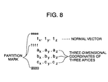
- Fig. 8 is a format of surface shape data in the third embodiment of the present invention.
- Fig. 9 is a perspective view showing the relation between triangular patch and node in the third embodiment of the present invention.
- Fig. 10 is a perspective view showing a normal vector of a patch at an overhang portion in the third embodiment of the present invention.
- Fig. 11 is a sectional view for explaining a superfluous curing thickness in the third embodiment of the present invention.
- Fig. 12 is a graph for explaining the relation between lamination thickness and dimensional difference in the third embodiment of the present invention.
- Fig. 13 is a PAD diagram when the correction amount takes a value which depends on an inclination of the overhang portion bottom in the third embodiment of the present invention.
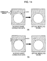
- Fig. 14 is a sectional view of a model when the correction amount takes a value which depends on an inclination of the overhang portion bottom in the third embodiment of the present invention.
- Fig. 15 is a PAD diagram when a normal vector is calculated from apices of a polygonal patch in the third embodiment of the present invention.
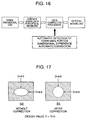
- Fig. 16 is a block diagram showing the procedure according to a fourth embodiment of the present invention in which the surface shape data correction processing is applied to perform optical modeling.
- Fig. 17 is a sectional view of a model having a hole of a diameter design value D=10.0 in the fourth embodiment of the present invention.
- Fig. 18 is a PAD diagram showing a processing method according to a fifth embodiment of the present invention in which correction is effected by a surface shape model.
- Fig. 19 is a perspective view showing the relation between triangular patch and node in the fifth embodiment of the present invention.
-
- Embodiments of the present invention will be described hereunder with reference to the drawings.
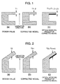
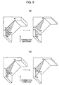
- Fig. 1 is a model section view showing an embodiment of the present invention. Fig. 1(a) is a sectional view of a three-dimensional shape model prepared using a design value T1 of thickness of an overhang portion. Fig. 1(b) is a sectional view of a three-dimensional shape model in which thickness correction is applied by removing a superfluous curing thickness β determined from equation (1) from the design value T1 of the overhang portion. Fig. 1(c) is a sectional view of an optical modeling product which is modeled based on a corrected model. In this manner, through a method in which the three-dimensional shape model having the design value T1 of thickness of an overhang portion can be corrected and modeled to a three-dimensional shape model for modeling having a difference of subtraction of a superfluous curing thickness β of an overhang portion from the design value T1, the overhang portion of the corrected model has a thickness equalling the design value T1, thereby making it possible to obtain an optical modeling product of high dimensional accuracy.
- Fig. 2 is a model section view showing an embodiment of the present invention. Fig. 2(a) is a sectional view of a three-dimensional shape model prepared using a design value T2 of thickness of an overhang portion. Fig. 2(b) is a sectional view of a three-dimensional shape model in which thickness correction is applied by removing a superfluous curing thickness γ determined from equation (1) from the design value T2 of the overhang portion. Fig. 2(c) is a sectional view of an optical modeling product which is modeled based on a corrected model of Fig. 2(b). In this manner, even when the overhang portion is not vertical to the direction of lamination, equation (1) can be applied and an optical modeling product of high dimensional accuracy having the overhang portion of a thickness equal to the design value T2 can be obtained from a shape model in which the design value T2 is corrected for the superfluous curing thickness γ.
- Fig. 3 is a flow chart for obtaining an optical modeling model of high dimensional accuracy by correcting the superfluous curing thickness of the overhang bottom in a three-dimensional shape model in accordance with the first embodiment of the present invention.
- Firstly, a three-dimensional shape model is modeled in accordance with design values and contour line data conversion is carried out on the basis of the model data. The presence or absence of an overhang portion is decided from the vertical positional relation between individual contour lines. In the absence of any overhang portion, no superfluous curing thickness is involved and modeling, as it is, is proceeded with. With an overhang portion detected, a three-dimensional shape model inputted in accordance with the design values is accessed. A designed thickness of the overhang portion is substituted into equation (1) to obtain a superfluous curing thickness and a three-dimensional shape model is prepared in which the thickness of the overhang portion is corrected. The three-dimensional shape model having the superfluous curing thickness corrected is converted into contour line data and optical modeling is carried out using this contour line data.
- Fig. 4 is a contour line and model section view showing a second embodiment of the present invention. Fig. 4(a) is a contour line and section diagram of a three-dimensional shape model prepared using a design value T1 of the thickness of an overhang portion. Fig. 4(b) is a contour line and section view in which a superfluous curing thickness β determined from equation (1) is removed from the design value T1 of the overhang portion. Fig. 4(c) is a contour line data section view in which removed data for a portion other than the overhang portion is added. Fig. 4(d) is a sectional view of an optical modeling product modeled based on a corrected model of Fig. 4(c).
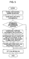
- Fig. 5 is a flow chart for a second embodiment directed to a method of correcting the superfluous curing thickness of an overhang portion by removing and adding model contour line data to obtain an optical modeling product of high dimensional accuracy and an apparatus based on the method.
- Fig. 6 shows a conventional example. When the design value of thickness of an overhang portion is set to T1 and the lamination direction is set as indicated by arrow, as shown at (a) in Fig. 6 and conversion into contour line data of a predetermined lamination pitch and optical modeling is performed as shown at (b), a laser beam for curing is irradiated in a direction inverse to the arrow (from the overhang top side) and consequently fresh resin, which is not desired fundamentally to be cured, is caused by a laser transmitting beam to suffer curing in a lower portion of the overhang, raising problems that superfluous curing takes place at the bottom of the overhang portion to cause the bottom to project and the thickness of the overhang portion amounts up to T1+α larger than the design value T1, as shown at (c), to degrade the dimensional accuracy.
- Fig. 7 is a PAD diagram of a third embodiment of the present invention directed to a processing method of correcting a dimensional difference of the overhang portion bottom due to superfluous curing on surface shape data.
- Firstly, a file of surface shape data to be corrected is designated. The surface shape data is data for expressing the surface of a three-dimensional shape model by a set of polygonal patches each having at least three vertexes, and triangular patches are described in connection with the present embodiment. Shown in Fig. 8 is a format of the surface shape data file. A normal vector and three-dimensional coordinates of three vertexes constituting individual patches are described and data pieces of the individual patches are separated from each other by terminator marks. Subsequently, coordinates of three vertexes and a normal vector of each patch in the surface shape data file are sequentially read and a total patch number is counted. Next, node numbers are allotted to the read-out coordinates of vertexes by allotting identical node numbers to the same coordinates of vertexes as those of patches previously read out. Further, information as to which nodes each patch is formed of is stored. Subsequently, for detection of an overhang portion, positive or negative of a Z component of a normal vector is decided. When the Z component is negative, that is, a patch plane faces downwards, the patch lies at the bottom of an overhang portion or the bottom of a modeling product and therefore, flags indicative of lying at the overhang portion bottom are attached to nodes constituting that patch. This procedure is repeated for all of the patches. Even when the above operation is effected on occasion while reading patch data, the processing as a whole is similar.
- Next, a superfluous curing thickness α serving as a correction amount is set. The manner of determining the superfluous curing thickness α has been described in connection with the foregoing embodiments. Thereafter, flags of all nodes are examined and Z coordinates of nodes attached with flags are added with correction amounts so that coordinates of individual nodes may be replaced with new coordinate values which are Z coordinate values after correction. Coordinates of vertexes constituting a patch are rewritten with the replaced new coordinates of nodes. The plane inclination of the patch is now changed and hence a normal vector of the patch is calculated using the Z coordinates after correction. A new surface shape data file is prepared in the same format as the read-out data format from the coordinates of vertexes and the normal vector after correction.
- Even when setting of correction amounts is effected at any phase before Z correction, the processing as a whole is similar.
- The reasons why node numbers are allotted to vertexes of patches and Z coordinate correction is processed at nodes will now be described. Fig. 9 is a diagram showing triangular patches of the surface shape data. Fig. 9(a) shows two adjacent patches A and B of which patch A lies at the bottom of an overhang portion and patch B is not at the overhang portion. The respective patches have vertexes a1, a2, a3 and b1, b2, b3. When coordinate values of the vertexes a1, a2 and a3 are moved upon changing of the shape of the patch A lying at the overhang portion bottom, the shape of the triangular patch A is changed while the patch A separating from the patch B to disturb the relation between the patches A and B, making data incorrect. A patch represented by normal surface shape data has at least three vertexes but is unaware of the fact that these vertexes are in common to this patch and an adjacent patch. In Fig. 9(b), apices in common to the triangular patches A and B are replaced with nodes n1 and n3 and the shape of the patch A is changed by moving nodes n1, n2 and n3.
- As a result, the shape of the patch B is concurrently changed so that the patches A and B may not separate from each other and the relation therebetween may be held to make data correct. Thus, in triangular patches representing the surface of a model, by replacing apices in common to adjacent patches with nodes and moving the nodes, the shape and position of both the patches can be changed without causing the two patches to separate from each other and intersect with each other. The inclined overhang bottom is exemplified herein but a horizontal one may be handled similarly.
- Next, a method of deciding a patch lying at the bottom of a modeling product or the bottom of an overhang portion by using a normal vector will be described. Shown in Fig. 10 are a triangular patch lying at the bottom of an overhang portion and its normal vector. Given that the direction of lamination of the model coincides with the positive direction of coordinate Z axis and a normal vector vertical to a plane defined by the patch and directing outwardly of the model is a (Xa, Ya, Za), that patch faces downwards when for the Z component, Za<0 stands and is determined to lie at the overhang portion bottom. By deciding positive or negative of the normal vector Z component in this manner, the patch lying at the overhang portion bottom can be detected automatically.
- Through the above processing method, the modeling product bottom and overhang portion bottom can be detected automatically, the dimensional difference can be corrected efficiently on surface shape data and an optical modeling product of high dimensional accuracy can be obtained by performing modeling on the basis of the data.
- While in the present embodiment the triangular patch has been described, a polygonal patch may be handled similarly.
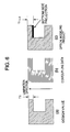
- A description will now be given of the superfluous curing thickness. Fig. 11(a) shows the principle of superfluous curing in optical modeling. Superfluous curing is caused by a phenomenon that a leakage of a laser beam transmitting through the overhang portion of a model cures fresh resin at the bottom of overhang portion. Fig. 11(b) is a diagram for explaining how to determine a superfluous curing thickness α.
- Fig. 12 shows the relation between lamination thickness and dimensional difference. The data is indicative of results obtained with the bottom of a horizontal overhang portion. As is clear from the figure, results of calculation of α=D-P(n-1) fairly coincide with actual measurement values.
- Fig. 13 is a PAD diagram for the case where the correction amount is a value which depends on an inclination of the overhang portion bottom in the third embodiment of the present invention. After a patch lying at the bottom of an overhang portion is detected, values depending on an inclination of the patch are set, as correction amounts, to nodes constituting that patch. Fig. 14(a) is a section view of model data obtained by applying the above correction of a correction amount of 1 to surface shape data of a model having a hole of a radius r of 3.0. However, the superfluous curing thickness depends on the inclination of the overhang portion bottom and therefore, when optical modeling is carried out based on this data, the dimensional difference becomes irregular and an optical modeling model deformed as shown in right section results. Fig. 14 (b) is a section view of model data obtained by applying the above correction of a correction amount which depends on the inclination of the overhang portion bottom, and when optical modeling is effected based on this data, a smooth hole shape as shown in the figure can be prepared and an optical modeling model of high dimensional accuracy can be obtained.
- Even when setting of the correction amounts is effected at any phase after the patch lying at the overhang portion bottom is detected, the processing as a whole is similar.
- By applying correction to the surface shape data through the above process method and performing modeling, an optical modeling product of high dimensional accuracy can be obtained.
- Fig. 15 is a PAD diagram for the case where normal vectors are calculated from vertexes of polygonal patches in the third embodiment of the present invention. Coordinates of vertexes constituting triangular patches included in the surface shape data file are read and normal vectors of the patches are calculated from the coordinates of vertexes. A patch lying at an overhang portion is decided using its normal vector. Even when calculation of the normal vector is effected at any phase before positive or negative of its Z component is determined, the processing as a whole is similar.
- By applying correction to the surface shape data through the above process method and performing modeling, an optical modeling product of high dimensional accuracy can be obtained.
- Fig. 16 shows a fourth embodiment of the present invention directed to the procedure for performing optical modeling by applying the correction processing to the above-described surface shape data. A shape model is prepared by three-dimensional CAD, the shape model is converted into surface shape data for optical modeling, the data is subjected to automatic detection of an overhang portion and applied with the correction processing of dimensional difference automatic correction, and optical modeling is carried out. Fig. 17 is a sectional view of a model formed with a hole having a diameter of design value D=10.0, especially, Fig. 17(a) being a section view of a model modeled without correction and Fig. 17(b) being a section view of a model applied with the aforementioned correction processing. Thus, by performing modeling in accordance with the procedure of the present invention, an optical modeling product of high dimensional accuracy can be obtained.
- Fig. 18 is a PAD diagram of a fifth embodiment of the present invention in which the dimensional difference of the overhang portion bottom or model bottom due to superfluous curing is eliminated by correcting surface shape data with a value determined by a predetermined rule in accordance with one of inclinations of adjacent overhang portion bottoms, especially, a maximum inclination with respect to the modeling direction axis herein.
- The reasons why node numbers are allotted to vertexes of patches and Z coordinate correction is processed at nodes will now be described. Fig. 19 is a diagram showing triangular patches of the surface shape data. Fig. 19(a) shows two adjacent patches A, B and C, D of which patch A lies at the bottom of an overhang portion and patch B is not at the overhang portion. The respective patches have vertexes a1, a2, a3 and b1, b2, b3. When coordinate values of the vertexes a1, a2 and a3 are moved upon changing of the shape of the patch A lying at the overhang portion bottom, the shape of the triangular patch A is changed while the patch A separating from the patch B to disturb the relation between the patches A and B, making data incorrect. A patch represented by normal surface shape data has at least three vertexes but is unaware of the fact that these apices are in common to this patch and an adjacent patch. In Fig. 19(b), vertexes in common to the triangular patches A and B are replaced with nodes n1 and n3 and the shape of the patch A is changed by moving nodes n1, n2 and n3. As a result, the shape of the patch B is concurrently changed so that the patches A and B may not separate from each other and the relation therebetween may be held to make data correct. Thus, in triangular patches representing the surface of a model, by replacing vertexes in common to adjacent patches with nodes and moving the nodes, the position can be changed without causing the two patches to separate from each other and intersect with each other. The inclined overhang bottom is exemplified herein but a horizontal one may be handled similarly.
- Next, the reasons why values applied to nodes common to patches are set to a value corresponding to one of inclination values of the patches which is the largest will be described. Given that values conforming to patch inclinations are β,β and γ (β < γ) for each patch in patches A, C and D processing, and node n2 and n5 are in same hight. In case when the correcting process is carried out in order of patches C, D and A, as node n2 is common to patches C, D and A, value applied to node n2 which conform to patch inclinations is β at patch C processing, γ at patch D processing and β at patch A processing, and also as node n5 is common to patches C and D, value applied to node n5 is β at patch C processing, γ at patch D processing. Last value of node n2 is β, and last value of node n5 is γ. Correcting amount of node n2 is smaller than that of node n5, as β and γ are in relation β < γ. Correcting process is in result that z coordinate value (i.e. hight) of node n2 differs from that of n5 and the patch D is adversely affected so as to be inclined as shown in Fig. 19(b). Fig. 19(c) shows an example where values applied to common nodes n2 and n5 and conforming to inclinations are set to a maximum value. Even when the patch processing is carried out in different order of A, C and D or C, D and A, values applied to nodes n2 and n5 at the same height and conforming to patch inclinations are both set to γ, so that Z coordinate values of nodes n2 and n5 after correction are at the same height and disturbance of the shape can be avoided.
- Through the processing method as above, bottom of model and the overhang portion bottom can be detected automatically and the dimensional difference can be corrected efficiently on surface shape data, thereby ensuring that an optical modeling product of high dimensional accuracy can be obtained by performing modeling on the basis of the data.
- While in the present embodiment the triangular patch has been described, a polygonal patch may be handled similarly.
- As described above, according to the present invention, by calculating a superfluous curing thickness caused by repetitious laser irradiation and performing correction by the thickness amount on three-dimensional model data or contour line data, an optical modeling product which exhibits high dimensional accuracy in the direction of lamination can be obtained to advantage.
- Further, the bottom of a modeling product and the bottom of an overhang portion can be detected automatically and a dimensional difference which is inherent to optical modeling technique and which is caused at the bottom can be corrected on surface shape data, so that correction of dimensional difference need not be subjected to further manual modification after returning to the three-dimensional CAD and the processing can advantageously be completed automatically within a short period of time.
Claims (4)
- An optical modeling method of building a solid shape model using surface shape data, representing the surface of a three-dimensional shape model by a set of polygonal patches, each having at least three vertexes and a normal vector of each patch, comprising the steps of:replacing the vertexes of each patch by nodes;determining that the patch lies at the bottom of either one of a building andan overhang portion when Z component of the normal vector of the patch is negative; when the patch is determined to lie at said bottom, attaching flags indicating that said patch is positioned at the bottom to the nodes constituting the patch,checking all nodes and correcting the surface shape data by moving the flagged nodes in Z direction;radiating a laser beam onto ultraviolet-ray curable resin and laminating cured resin based an the corrected surface shape data.
- The optical modeling method according to claim 1, wherein the flagged nodes are moved in Z direction by a superfluous curing thickness α, given as follows:
- An optical modeling apparatus for building a solid shape model using surface shape data, representing the surface of a three-dimensional shape model by a set of polygonal patches, each having at least three vertexes and a normal vector of each patch, comprising:means for replacing the vertexes of each patch by nodes;means for determining that the patch lies at the bottom of either one of a building and an overhang portion when Z component of the normal vector of the patch is negative;means for, when the patch is determined to lie at said bottom, attaching flags indicating that said patch is positioned at the bottom to the nodes constituting the patch, checking all nodes and correcting the surface shape data by moving the flagged nodes in Z direction;means for radiating a laser beam onto ultraviolet-ray curable resin andlaminating cured resin based an the corrected surface shape data.
- The optical modeling apparatus according to claim 3, wherein
said correcting means includes means for moving the flagged nodes in Z direction by a superfluous curing thickness α, given as follows:
Applications Claiming Priority (7)
| Application Number | Priority Date | Filing Date | Title |
|---|---|---|---|
| JP27404193A JP3173252B2 (en) | 1993-11-02 | 1993-11-02 | Stereolithography method and stereolithography device |
| JP27404193 | 1993-11-02 | ||
| JP27647593 | 1993-11-05 | ||
| JP27647593A JP3146805B2 (en) | 1993-11-05 | 1993-11-05 | Stereolithography method and stereolithography device |
| JP6831094 | 1994-04-06 | ||
| JP06831094A JP3477805B2 (en) | 1994-04-06 | 1994-04-06 | Data processing method and stereolithography apparatus |
| EP94931198A EP0727302B1 (en) | 1993-11-02 | 1994-11-01 | Method of correcting thickness of excessive curing of photomolded article |
Related Parent Applications (1)
| Application Number | Title | Priority Date | Filing Date |
|---|---|---|---|
| EP94931198A Division EP0727302B1 (en) | 1993-11-02 | 1994-11-01 | Method of correcting thickness of excessive curing of photomolded article |
Publications (2)
| Publication Number | Publication Date |
|---|---|
| EP1136235A1 true EP1136235A1 (en) | 2001-09-26 |
| EP1136235B1 EP1136235B1 (en) | 2003-06-18 |
Family
ID=27299699
Family Applications (2)
| Application Number | Title | Priority Date | Filing Date |
|---|---|---|---|
| EP01112022A Expired - Lifetime EP1136235B1 (en) | 1993-11-02 | 1994-11-01 | Method and apparatus of correcting superfluous curing thickness of optical modeling product |
| EP94931198A Expired - Lifetime EP0727302B1 (en) | 1993-11-02 | 1994-11-01 | Method of correcting thickness of excessive curing of photomolded article |
Family Applications After (1)
| Application Number | Title | Priority Date | Filing Date |
|---|---|---|---|
| EP94931198A Expired - Lifetime EP0727302B1 (en) | 1993-11-02 | 1994-11-01 | Method of correcting thickness of excessive curing of photomolded article |
Country Status (4)
| Country | Link |
|---|---|
| US (1) | US5858297A (en) |
| EP (2) | EP1136235B1 (en) |
| DE (2) | DE69430703T2 (en) |
| WO (1) | WO1995012485A1 (en) |
Cited By (1)
| Publication number | Priority date | Publication date | Assignee | Title |
|---|---|---|---|---|
| CN113635558A (en) * | 2020-05-11 | 2021-11-12 | 通用电气公司 | Compensation for additive manufacturing |
Families Citing this family (14)
| Publication number | Priority date | Publication date | Assignee | Title |
|---|---|---|---|---|
| US6270335B2 (en) | 1995-09-27 | 2001-08-07 | 3D Systems, Inc. | Selective deposition modeling method and apparatus for forming three-dimensional objects and supports |
| US5943235A (en) | 1995-09-27 | 1999-08-24 | 3D Systems, Inc. | Rapid prototyping system and method with support region data processing |
| SG87044A1 (en) * | 1995-09-27 | 2002-03-19 | 3D Systems Inc | Selective deposition modeling method and apparatus for forming three-dimensional objects and supports |
| US6051179A (en) * | 1997-03-19 | 2000-04-18 | Replicator Systems, Inc. | Apparatus and method for production of three-dimensional models by spatial light modulator |
| US20030207959A1 (en) | 2000-03-13 | 2003-11-06 | Eduardo Napadensky | Compositions and methods for use in three dimensional model printing |
| US8481241B2 (en) | 2000-03-13 | 2013-07-09 | Stratasys Ltd. | Compositions and methods for use in three dimensional model printing |
| US7300619B2 (en) | 2000-03-13 | 2007-11-27 | Objet Geometries Ltd. | Compositions and methods for use in three dimensional model printing |
| US6463872B1 (en) | 2000-03-31 | 2002-10-15 | Alcatel | Laser photocuring system |
| US8460451B2 (en) | 2011-02-23 | 2013-06-11 | 3D Systems, Inc. | Support material and applications thereof |
| US9394441B2 (en) | 2011-03-09 | 2016-07-19 | 3D Systems, Inc. | Build material and applications thereof |
| US9157007B2 (en) | 2011-03-09 | 2015-10-13 | 3D Systems, Incorporated | Build material and applications thereof |
| US10850450B2 (en) | 2013-05-31 | 2020-12-01 | Hewlett-Packard Development Company, L.P. | Modifying a base layer of an object |
| JP7040236B2 (en) * | 2018-04-05 | 2022-03-23 | 富士フイルムビジネスイノベーション株式会社 | 3D shape data editing device, 3D modeling device, 3D modeling system, and 3D shape data editing program |
| US11498283B2 (en) * | 2019-02-20 | 2022-11-15 | General Electric Company | Method and apparatus for build thickness control in additive manufacturing |
Citations (5)
| Publication number | Priority date | Publication date | Assignee | Title |
|---|---|---|---|---|
| EP0277832A2 (en) * | 1987-02-05 | 1988-08-10 | Hewlett-Packard Company | Method for graphic display |
| EP0422234A1 (en) * | 1989-03-02 | 1991-04-17 | Fanuc Ltd. | Three-dimensional parametric modeling method |
| WO1991012120A1 (en) * | 1990-02-15 | 1991-08-22 | 3D Systems, Inc. | Method of and apparatus for forming a solid three-dimensional article from a liquid medium |
| US5238639A (en) * | 1990-10-31 | 1993-08-24 | 3D Systems, Inc. | Method and apparatus for stereolithographic curl balancing |
| JPH05224721A (en) * | 1992-02-12 | 1993-09-03 | Nec Software Ltd | Machining method for three-dimensional curved surface shape |
Family Cites Families (7)
| Publication number | Priority date | Publication date | Assignee | Title |
|---|---|---|---|---|
| JP2526164B2 (en) * | 1990-07-19 | 1996-08-21 | 株式会社 ヤマシタ | How to make a fishhook |
| JPH0479827A (en) * | 1990-07-20 | 1992-03-13 | Daiwa Seiko Inc | Device of connecting fishing rod |
| JP2715648B2 (en) * | 1990-09-29 | 1998-02-18 | ソニー株式会社 | 3D shape forming device |
| JPH0745195B2 (en) * | 1990-11-02 | 1995-05-17 | 三菱商事株式会社 | High-precision photo-solidification modeling device |
| JPH0533901A (en) * | 1991-07-24 | 1993-02-09 | Shigehisa Tamahashi | Heating medium power generation method and device thereof |
| JPH0533900A (en) * | 1991-07-30 | 1993-02-09 | Toshiba Corp | Gas supply device |
| JPH05278124A (en) * | 1992-04-01 | 1993-10-26 | Matsushita Electric Ind Co Ltd | Method for producing optically modeling data |
-
1994
- 1994-11-01 EP EP01112022A patent/EP1136235B1/en not_active Expired - Lifetime
- 1994-11-01 DE DE69430703T patent/DE69430703T2/en not_active Expired - Fee Related
- 1994-11-01 US US08/637,623 patent/US5858297A/en not_active Expired - Fee Related
- 1994-11-01 WO PCT/JP1994/001841 patent/WO1995012485A1/en active IP Right Grant
- 1994-11-01 DE DE69432836T patent/DE69432836T2/en not_active Expired - Fee Related
- 1994-11-01 EP EP94931198A patent/EP0727302B1/en not_active Expired - Lifetime
Patent Citations (5)
| Publication number | Priority date | Publication date | Assignee | Title |
|---|---|---|---|---|
| EP0277832A2 (en) * | 1987-02-05 | 1988-08-10 | Hewlett-Packard Company | Method for graphic display |
| EP0422234A1 (en) * | 1989-03-02 | 1991-04-17 | Fanuc Ltd. | Three-dimensional parametric modeling method |
| WO1991012120A1 (en) * | 1990-02-15 | 1991-08-22 | 3D Systems, Inc. | Method of and apparatus for forming a solid three-dimensional article from a liquid medium |
| US5238639A (en) * | 1990-10-31 | 1993-08-24 | 3D Systems, Inc. | Method and apparatus for stereolithographic curl balancing |
| JPH05224721A (en) * | 1992-02-12 | 1993-09-03 | Nec Software Ltd | Machining method for three-dimensional curved surface shape |
Cited By (5)
| Publication number | Priority date | Publication date | Assignee | Title |
|---|---|---|---|---|
| CN113635558A (en) * | 2020-05-11 | 2021-11-12 | 通用电气公司 | Compensation for additive manufacturing |
| EP3909746A1 (en) * | 2020-05-11 | 2021-11-17 | General Electric Company | Compensation for additive manufacturing |
| EP4219132A1 (en) * | 2020-05-11 | 2023-08-02 | General Electric Company | Compensation for additive manufacturing |
| CN113635558B (en) * | 2020-05-11 | 2023-09-26 | 通用电气公司 | Compensation for additive manufacturing |
| US11782416B2 (en) | 2020-05-11 | 2023-10-10 | General Electric Company | Compensation for additive manufacturing |
Also Published As
| Publication number | Publication date |
|---|---|
| DE69430703T2 (en) | 2003-01-30 |
| DE69432836D1 (en) | 2003-07-24 |
| EP0727302B1 (en) | 2002-05-29 |
| EP1136235B1 (en) | 2003-06-18 |
| WO1995012485A1 (en) | 1995-05-11 |
| US5858297A (en) | 1999-01-12 |
| DE69432836T2 (en) | 2004-05-13 |
| EP0727302A1 (en) | 1996-08-21 |
| EP0727302A4 (en) | 1996-09-18 |
| DE69430703D1 (en) | 2002-07-04 |
Similar Documents
| Publication | Publication Date | Title |
|---|---|---|
| US5858297A (en) | Method and apparatus of correcting superfluous curing thickness of optical modeling product | |
| JP3436705B2 (en) | How to form a three-dimensional object | |
| US6366825B1 (en) | Simultaneous multiple layer curing in stereolithography | |
| US6813594B2 (en) | Automatic determination and selection of build parameters for solid freeform fabrication techniques based on automatic part feature recognition | |
| EP2481555B1 (en) | Region-based supports for parts produced by solid freeform fabrication | |
| US6898477B2 (en) | System and method for performing adaptive modification of rapid prototyping build files | |
| US6600965B1 (en) | Method and apparatus for production of high resolution three-dimensional objects by stereolithography | |
| US6084980A (en) | Method of and apparatus for deriving data intermediate to cross-sectional data descriptive of a three-dimensional object | |
| EP0354637A2 (en) | CAD/CAM stereolithographic data conversion | |
| US20050015173A1 (en) | Rapid prototyping method and device using v-cad data | |
| US11106193B1 (en) | Neural network-based error compensation method, system and device for 3D printing | |
| JP2006099123A (en) | Enhanced building techniques in stereolithography | |
| EP1270186B1 (en) | Method and apparatus for forming three-dimensional objects | |
| US6781582B1 (en) | Mesh generator for and method of generating meshes in an extrusion process | |
| US20220410483A1 (en) | Stl model slicing method and device | |
| CN111859577A (en) | Direct layering method for laser additive repair | |
| JP3570138B2 (en) | 3D stereolithography data creation method | |
| Tyberg | Local adaptive slicing for layered manufacturing | |
| JPH05278123A (en) | Laser scanning method for optical model | |
| JP4405671B2 (en) | Determination of resin hardened area in optical stereolithography | |
| JP3477805B2 (en) | Data processing method and stereolithography apparatus | |
| CN110230980B (en) | Three-dimensional point cloud based dead mass background measurement method and system and storage medium | |
| JP2001187425A (en) | Method for treating shape data for photo fabrication, and method and device for photo fabrication | |
| JPH05278124A (en) | Method for producing optically modeling data | |
| JPH07137142A (en) | Space laminate forming machine |
Legal Events
| Date | Code | Title | Description |
|---|---|---|---|
| PUAI | Public reference made under article 153(3) epc to a published international application that has entered the european phase |
Free format text: ORIGINAL CODE: 0009012 |
|
| 17P | Request for examination filed |
Effective date: 20010608 |
|
| AC | Divisional application: reference to earlier application |
Ref document number: 727302 Country of ref document: EP |
|
| AK | Designated contracting states |
Kind code of ref document: A1 Designated state(s): DE GB |
|
| RIN1 | Information on inventor provided before grant (corrected) |
Inventor name: TOSHIRO ENDO Inventor name: OHKUBO, MASAKATSU Inventor name: NORIO GOTO Inventor name: MORITANI, MASUMI Inventor name: OZAWA, MASAHIKO |
|
| 17Q | First examination report despatched |
Effective date: 20020426 |
|
| AKX | Designation fees paid |
Free format text: DE GB |
|
| GRAH | Despatch of communication of intention to grant a patent |
Free format text: ORIGINAL CODE: EPIDOS IGRA |
|
| GRAH | Despatch of communication of intention to grant a patent |
Free format text: ORIGINAL CODE: EPIDOS IGRA |
|
| GRAA | (expected) grant |
Free format text: ORIGINAL CODE: 0009210 |
|
| AC | Divisional application: reference to earlier application |
Ref document number: 0727302 Country of ref document: EP Kind code of ref document: P |
|
| AK | Designated contracting states |
Designated state(s): DE GB |
|
| REG | Reference to a national code |
Ref country code: GB Ref legal event code: FG4D |
|
| REF | Corresponds to: |
Ref document number: 69432836 Country of ref document: DE Date of ref document: 20030724 Kind code of ref document: P |
|
| PLBE | No opposition filed within time limit |
Free format text: ORIGINAL CODE: 0009261 |
|
| STAA | Information on the status of an ep patent application or granted ep patent |
Free format text: STATUS: NO OPPOSITION FILED WITHIN TIME LIMIT |
|
| 26N | No opposition filed |
Effective date: 20040319 |
|
| PGFP | Annual fee paid to national office [announced via postgrant information from national office to epo] |
Ref country code: GB Payment date: 20061106 Year of fee payment: 13 |
|
| PGFP | Annual fee paid to national office [announced via postgrant information from national office to epo] |
Ref country code: DE Payment date: 20061207 Year of fee payment: 13 |
|
| GBPC | Gb: european patent ceased through non-payment of renewal fee |
Effective date: 20071101 |
|
| PG25 | Lapsed in a contracting state [announced via postgrant information from national office to epo] |
Ref country code: DE Free format text: LAPSE BECAUSE OF NON-PAYMENT OF DUE FEES Effective date: 20080603 |
|
| PG25 | Lapsed in a contracting state [announced via postgrant information from national office to epo] |
Ref country code: GB Free format text: LAPSE BECAUSE OF NON-PAYMENT OF DUE FEES Effective date: 20071101 |