EP1150460A1 - Electronic equipment, and method for controlling state of physical layer circuit thereof - Google Patents

Electronic equipment, and method for controlling state of physical layer circuit thereof Download PDF

Info

Publication number
EP1150460A1
EP1150460A1 EP01303697A EP01303697A EP1150460A1 EP 1150460 A1 EP1150460 A1 EP 1150460A1 EP 01303697 A EP01303697 A EP 01303697A EP 01303697 A EP01303697 A EP 01303697A EP 1150460 A1 EP1150460 A1 EP 1150460A1
Authority
EP
European Patent Office
Prior art keywords
state
signal
node
physical layer
layer circuit
Prior art date
Legal status (The legal status is an assumption and is not a legal conclusion. Google has not performed a legal analysis and makes no representation as to the accuracy of the status listed.)
Withdrawn
Application number
EP01303697A
Other languages
German (de)
French (fr)
Inventor
Akira IPD Sony Corporation Nakamura
Tetsuya IPD Sony Corporation Sato
Current Assignee (The listed assignees may be inaccurate. Google has not performed a legal analysis and makes no representation or warranty as to the accuracy of the list.)
Sony Corp
Original Assignee
Sony Corp
Priority date (The priority date is an assumption and is not a legal conclusion. Google has not performed a legal analysis and makes no representation as to the accuracy of the date listed.)
Filing date
Publication date
Application filed by Sony Corp filed Critical Sony Corp
Publication of EP1150460A1 publication Critical patent/EP1150460A1/en
Withdrawn legal-status Critical Current

Links

Images

Classifications

    • HELECTRICITY
    • H04ELECTRIC COMMUNICATION TECHNIQUE
    • H04LTRANSMISSION OF DIGITAL INFORMATION, e.g. TELEGRAPHIC COMMUNICATION
    • H04L69/00Network arrangements, protocols or services independent of the application payload and not provided for in the other groups of this subclass
    • H04L69/30Definitions, standards or architectural aspects of layered protocol stacks
    • H04L69/32Architecture of open systems interconnection [OSI] 7-layer type protocol stacks, e.g. the interfaces between the data link level and the physical level
    • H04L69/322Intralayer communication protocols among peer entities or protocol data unit [PDU] definitions
    • H04L69/323Intralayer communication protocols among peer entities or protocol data unit [PDU] definitions in the physical layer [OSI layer 1]

Definitions

  • the present invention relates to electronic equipment provided with a physical layer circuit constituting a physical layer, for example (though not exclusively) a physical layer which conforms to the IEEE 1394 standard, and a method for controlling the state of the physical layer circuit.
  • IEEE 1394 high-performance serial bus standard (IEEE 1394 standard) is known.
  • the IEEE 1394 standard defines data transmission at rates of 100Mbps (98.304Mbps), 200Mbps (196.608Mbps), and 400Mbps (393.216Mbps), and defines 1394 port with higher transmission rate to have compatibility with its lower transmission rate. This standard allows data transmissions at rates of 100Mbps, 200Mbps, and 400Mbps in one and the same network.
  • IEEE 1394 standard employs transmission format in Data/Strobe link (DS-Link) coding method.
  • transmission format in the Data/Stroke link coding method as shown in Fig. 1, transmission data is converted into two signals including data and strobe for compensating the signal thereof, and the exclusive OR of these two signals is obtained, thereby generating clocks.
  • the IEEE 1394 standard also defines a cable 200 having a structure such as shown in a cross-sectional view of Fig. 2, including: a first shielding layer 201; two pairs of twisted pair lines (i.e.
  • the IEEE 1394 standard performs arbitration for obtaining bus, prior to data transmission, and as a control signal for arbitration, defines an arbitration signal.
  • the IEEE 1394 standard automatically reconfigures the entire bus topology by resetting the bus at the time when a node is added or deleted on the bus.
  • the arbitration signal is also defined as a control signal required for the topology reconfiguration.
  • the logical values of the arbitration signal in the physical layer are three values of "0", “1", and "Z". These values are produced in accordance with the rules shown in Tables 1 and 2 below, and are decoded in accordance with the rule shown in Table 3 below.
  • Transmit arbitration signal A (Arb_A_Tx) Drivers Comment Strb_Tx Strb_Enable Z - 0 TPA driver is disabled 0 0 1 TPA driver is enabled, strobe is low 1 1 1 TPA driver is enabled, strobe is high
  • Transmit arbitration signal B (Arb_B_Tx) Drivers Comment Data_Tx Data_Enable Z - 0 TPB driver is disabled 0 0 1 TPB driver is enabled, data is low 1 1 1 TPB driver is enabled, data is high Received arbitration comparator value (Arb_n _Rx) Transmitted arbitrat-ion signal for this port (Arb_n _Tx) Interpreted arbitration signal (Arb_n ) Comment Z Z Z Z If
  • the physical layer encodes the line state by use of two transmission arbitration signals Arb_A_Tx and Arb_B_Tx in accordance with the rule shown in Table 4 below, and decodes the line state from receive arbitration signals Arb_A and Arb_B in accordance with the rule shown in Table 5 below.
  • the topology is automatically configured through the bus initialization phase, tree identification phase, and self-identification phase in this order.
  • the bus reset signal changes all the nodes into particular states, to entirely clear the topology information.
  • each node has only information about whether or not the node itself is a branch (i.e. whether or not it is directly connected to a plurality of the nodes adjacent thereto), whether or not the node is a leaf (i.e. whether or not only a single node is adjacent thereto), and whether or not the node is independent (i.e. whether or not it is connected to neither of a plurality of nodes adjacent thereto).
  • Fig. 3A is a diagram showing a network constituted by leaf nodes and branch nodes.
  • the entire network topology is converted into one tree where one node is designated as a route. All the physical connections connected to the route indicate the direction of route node.
  • Each connected port is assigned with a label to indicate the direction, and is referred to as a "parent" port (in the case where the port is connected to the node close to the route), or a "child” port (in the case where the port is connected to the node remote from the route).
  • the port which is not connected to any node is assigned with a label "off", and does not participate in the arbitration process conducted afterwards.
  • Fig. 3B shows the network constituted at the completion of the tree identification process.
  • each node is provided with an opportunity to select its own specific physical_ID to identify itself with respect to an arbitrary control element associated with the bus. This process is also necessary to control electric power of low level, and to produce a topology map of the system required for determining the rate of each data path.
  • the self-identification process employs a decision theoretic selection process. Specifically, a root node leaves the media control to the node associated with the connection port having the smallest number, and waits until the node sends the "ident_done" signal for notifying that the node itself and all the child nodes thereof have completed self-identification. After that, the root node leaves the control to the node associated with the upper port having the next number, and waits until the processing of the node is completed. When the nodes associated with all the ports of the root complete their processings, the root itself conducts self-identification. The child node conducts the same process as above recursively. The completion of the self-identification process is acknowledged when the bus goes into an idle state over a subaction gap period.
  • Each node can send its self-identification information by sending one to four very short packets (Self-ID Packet) involving physical_ID or other control information to a cable.
  • the physical_ID is a value obtained by simply counting the number of times the node which is in the state of receiving the self-identification information is passed before the node sends the self-identification packet. For example, the node which sends its self-identification packet first selects a 0 as a physical_ID, and the node which sends its self-identification packet second selects a 1 as a physical_ID. Same process is repeated to determine the physical_ID of the nodes which send their self-identification packet third and thereafter.
  • Fig. 3C shows the network obtained at the completion of the self-identification process. Each "child" port is assigned with a "ch-i" label by which the node connected to the port can be identified.
  • the behavior of the physical layer at the time when it receives a signal for canceling a request at an arbitration phase is defined as follows: "when a child node which is making a request cancels the request, the physical layer (PHY) at the permission side observes its TX_GRANT signal to be returned thereto as a RX_REQUEST_CANCEL signal [Z0], and returns its state to idle state” (The transition of A1:A0 and transition of A2:A0 in Fig. 4).
  • a 4 is a transition diagram at an arbitration phase, showing a A0 (Idle) state, a A1 (Request) state, a A2 (Grand) state, a RX (Receive) state, a TX (Transmit) state, and PH (PHY Response) state, respectively.
  • 5 is a transition diagram at a port connection, showing P0 state (Disconnected), P1 state (Resuming), P2 state (Active), P3 state (Suspended Initiator), P4 state (Suspended Target), P5 state (Suspended), and P6 state (Disabled), respectively.
  • a node B at the time when a node A makes a request for obtaining a right to use bus for transmission, and after that, the node A cancels the request, taking as an example the case where 5 nodes are connected to each other where a node C is a route node as shown in Fig. 6A.
  • arrows show transmission and receipt of data
  • the terms IDLE, REQ, GRANT, RECEIVE, and TRANS in the respective nodes show the states of physical layers of the respective nodes.
  • the diagonally shaded arrow shows a request signal and a grant signal (same signals are allocated in the IEEE 1394-1995 and 1394a standard), the grid-patterned arrow shows a data prefix signal, and the filled-in arrow shows a data payload.
  • Embodiments of the present invention relate to electronic equipment in which the physical layer circuit is operated in such a manner that, when receiving a first signal from a child node, the physical layer circuit changes its state from a first state into a second state and sends a first signal to a parent node, and when receiving a third signal for canceling the first signal from the child node before receiving the second signal corresponding to the first signal from the parent node, the physical layer circuit sends the third signal to the parent node after receiving the second signal from the parent node, and furthermore, the physical layer circuit returns its state from the second state to the first state after receiving the third signal from the parent node, thereby avoiding the occurrence of troubles which may be caused if the physical layer circuit receives the second signal from the parent node in the first state.
  • Embodiments of the present invention also relate to electronic equipment in which the physical layer circuit is operated in such a manner that, when receiving a first signal from a child node, the physical layer circuit changes its state from a first state into a second state and sends the first signal to a parent node, and when receiving a third signal for canceling the first signal from the child node after receiving the second signal corresponding to the first signal from the parent node and shifting its state from the second state to the third state, the physical layer circuit sends the third signal to the parent node, and furthermore, the physical layer circuit returns its state from the third state to the first state after receiving the third signal from the parent node, thereby avoiding the occurrence of troubles which may be caused if the physical layer circuit receives the second signal from the parent node in the first state.
  • Embodiments of the present invention can provide electronic equipment capable of preventing the occurrence of troubles such as described above, and a method for controlling the state of the physical layer circuit thereof.
  • electronic equipment comprising a physical layer circuit, and a processor upper than the physical layer circuit
  • the physical layer circuit includes: a first transmitter for performing communication with a child node; a second transmitter for performing communication with a parent node; and a controller for controlling the physical layer circuit in such a manner that, when receiving a first signal from the child node by use of the first transmitter, the physical layer circuit changes its state from a first state into a second state and transmits the first signal to the parent node by use of the second transmitter, for controlling the physical layer circuit in such a manner that, when receiving a third signal for canceling the first signal from the child node by use of the first transmitter before receiving a second signal corresponding to the first signal from the parent node by use of the second transmitter, the physical layer circuit transmits the third signal to the parent node by use of the second transmitter after receiving the second signal from the parent node by use of the second transmitter, and for controlling the physical layer circuit in such a manner that, after receiving the third signal from the parent no
  • the physical layer circuit constitutes a physical layer which conforms to the IEEE 1394 standard.
  • the first state is an idle state
  • the second state is a request state.
  • the first signal is a request signal for obtaining right to use bus for transmission
  • the second signal is a grant signal
  • the third signal is an idle signal.
  • a method for controlling a state of a physical layer circuit including transmitters for performing communication with a child node and a parent node respectively includes the steps of: when receiving a first signal from a child node, controlling the physical layer circuit to change its state from a first state into a second state, and to transmit the first signal to the parent node; when receiving a third signal for canceling the first signal from the child node before receiving a second signal corresponding to the first signal from the parent node, controlling the physical layer circuit to transmit the third signal to the parent node after receiving the second signal from the parent node; and controlling the physical layer circuit to return its state from the second state to the first state after receiving the third signal from the parent node.
  • the physical layer circuit is free from the situation in which it receives a second signal from the parent node in the first state.
  • This arrangement serves to prevent the occurrence of troubles which may cause if the physical layer circuit receives the second signal from the parent node in the first state.
  • the physical layer circuit constitutes a physical layer which conforms to the IEEE 1394 standard
  • the physical layer circuit if the physical layer circuit receives an idle signal for canceling a request signal from a child node in a request state, the physical layer circuit returns its state into an idle state after it has received an idle signal from the parent node. There arises no situation in which the physical layer circuit receives a grant signal [00] from the parent node in the idle state.
  • This arrangement serves to prevent the occurrence of trouble that the physical layer circuit misunderstands that it has received a suspend signal and changes its state into a suspend state.
  • electronic equipment comprising a physical layer circuit, and a processor upper than the physical layer circuit
  • the physical layer circuit includes: a first transmitter for performing communication with a child node; a second transmitter for performing communication with a parent node; and a controller for controlling the physical layer circuit in such a manner that, when receiving a first signal from the child node by use of the first transmitter, the physical layer circuit changes its state from a first state into a second state and transmits the first signal to the parent node by use of the second transmitter, for controlling the physical layer circuit in such a manner that, when receiving a third signal for canceling the first signal from the child node by use of the first transmitter after receiving a second signal corresponding to the first signal from the parent node by use of the second transmitter and changing its state from the second state into the third state, the physical layer circuit transmits the third signal to the parent node by use of the second transmitter; and for controlling the physical layer circuit in such a manner that, after receiving the third signal from the parent node by use of the second transmitter
  • the physical layer circuit constitutes a physical layer which conforms to the IEEE 1394 standard.
  • the first state is an idle state
  • the second state is a request state
  • the third state is a grant state.
  • the first signal is a request signal for obtaining right to use bus for transmission
  • the second signal is a grant signal
  • the third signal is an idle signal.
  • a method for controlling a state of a physical layer circuit is a method for controlling a state of a physical layer circuit including transmitters for performing communication with a child node and a parent node respectively.
  • the physical layer circuit When receiving a first signal from a child node, the physical layer circuit is controlled to change its state from a first state into a second state, and to transmit the first signal to the parent node.
  • the physical layer circuit When receiving a third signal for canceling the first signal from the child node after receiving a second signal corresponding to the first signal from the parent node and changing its state from the second state to the third state, the physical layer circuit is controlled to transmit the third signal to the parent node.
  • the physical layer circuit is controlled to return its state from the third state to the first state after receiving the third signal from the parent node.
  • the physical layer circuit is free from the problem that it receives a second signal from the parent node in the first state.
  • This arrangement serves to prevent the occurrence of trouble which may cause if the physical layer circuit receives the second signal from the parent node in the first state.
  • the physical layer circuit constitutes a physical layer which conforms to the IEEE 1394 standard
  • the physical layer circuit if the physical layer circuit receives an idle signal for canceling a request signal from a child node in a grant state, the physical layer circuit returns its state into an idle state after it has received an idle signal from the parent node. There arises no situation in which the physical layer circuit receives a grant signal [00] from the parent node in the idle state.
  • This arrangement serves to prevent the trouble that the physical layer circuit misunderstands that it has received a suspend signal, although it actually is a grant signal, and changes its state into a suspend state.
  • Fig. 10 is a diagram showing an exemplary structure of a network constituted based on the IEEE 1394 standard.
  • a work station 10, a personal computer 11, a hard disc drive 12, a CD-ROM drive 13, a camera 14, a printer 15, and a scanner 16 together constitute an IEEE 1394 node, and are connected to each other via IEEE 1394 buses 20.
  • the connection methods in conformity with the IEEE 1394 standard are categorized into two: a daisy chain connection and a node multipoint connection.
  • 16 nodes i.e. equipment having an IEEE 1394 port
  • 63 nodes which is the maximum number in the IEEE 1394 standard, can be connected.
  • the IEEE 1394 standard allows the cable connection/disconnection in the state where equipment operates, that is, the equipment is turned on.
  • the reconfiguration of the topology is conducted through the bus initialization phase, the tree identification phase, and the self-identification phase in this order, as described above.
  • the identification and arrangement of the nodes connected to the network is controlled on the interface.
  • Fig. 11 is a diagram showing the constituent elements and the protocol architecture of the interface which conforms to the IEEE 1394 standard.
  • the interface is constituted by hardware and firmware.
  • the hardware is constituted by a physical layer (PHY) and a link layer.
  • the physical layer directly drives a signal which conforms to the IEEE 1394 standard.
  • the link layer includes a host interface and a physical layer interface.
  • the firmware is constituted by a transaction layer and a management layer.
  • the transaction layer is constituted by a management driver for performing an actual operation for the interface which conforms to the IEEE 1394 standard.
  • the management layer is constituted by a driver for managing a network, and is referred to as a serial bus management (SBM) and conforms to the IEEE 1394 standard.
  • SBM serial bus management
  • the application layer is constituted by a software used by a user, and a management software for interfacing the transaction layer and the management layer.
  • the transmission operation performed within the network is referred to as a subaction, and the following two subactions are defined.
  • One of the subactions is in a non-synchronous transmission mode referred to as an "asynchronous" mode, while the other is in a real-time transmission mode referred to as an "isochronous" mode in which the transmission band is secured.
  • Each of the subactions is further categorized in the three parts which assume the following states, respectively:
  • Fig. 12 is a diagram showing the transaction state with the lapse of time in the asynchronous transmission mode.
  • the initial subaction gap shows that the bus is in the idle state. The time during which the subaction gap lasts is monitored to judge whether or not the immediately preceding transmission has finished and another new transmission is possible.
  • the node which wishes to conduct transmission judges that the bus is usable, and performs an arbitration for obtaining the bus. In an actual operation, the judgment whether or not to stop the bus is conducted by the node A located at the root, as shown in Figs. 13A and 13B. After the node wishing the transmission obtains the right to use the bus in this arbitration, the node conducts transmission of the next data, that is, packet transmission. After the data transmission, the node which has received the data conducts acknowledgement in response to the data transmission by returning a data receipt acknowledgement return code (ack).
  • ack data receipt acknowledgement return code
  • acknowledgement By the execution of the acknowledgement, it can be acknowledged from the data receipt acknowledgement return code (ack) that the transmission has normally conducted in both the transmission node and the receiving node.
  • ack data receipt acknowledgement return code
  • the transmission in the isochronous mode basically in the same structure as of the transmission in the asynchronous mode is executed, except that, as shown in Fig. 14, the transmission in the isochronous subaction is assigned with higher priority and is executed prior to the transmission in the asynchronous subaction.
  • the isochronous transmission in the isochronous subaction is executed subsequent to the cycle start packet which is issued at every about 8 kHz (125 ⁇ s), and is assigned with higher priority to be executed prior to the asynchronous transmission in the asynchronous subaction. In this manner, the isochronous transmission is in the transmission mode in which the transmission band is secured, thereby attaining the transmission of the real-time data.
  • the cycle described above is created by the cycle start packet supplied from the node having a cycle master function (i.e. any equipment connected to the bus).
  • the band required for data transmission (although this is a unit of time, it is referred to as a band) is secured from all the foremost end of the cycle. Therefore, in the isochronous transmission, the data transmission is secured for a specified period of time. However, since the isochronous transmission has no arrangement for data protection, the data is lost when transmission error occurs.
  • the node which has obtained the right to use the bus as a result of arbitration during the time when the bus is not used for isochronous transmission in each cycle sends the asynchronous packet. The reliable transmission is possible by employment of the acknowledgement and retry; however, the transmission is not executed at a constant timing.
  • the transmission data is provided with a channel ID for identifying its content (i.e. transmission node), so that only the require real-time data is received.
  • the node In order to allow a predetermined node to execute isochronous transmission, it is required that the node has the isochronous function. In addition, at least one of nodes having the isochronous function must have also cycle master function. Furthermore, at least one of nodes connected to the IEEE 1394 serial bus must have isochronous resource managing function.
  • the address space defined in the IEEE 1394 standard has a structure such as shown in Fig. 15.
  • This structure conforms to the CSR architecture defined by the ISO/IEC13213 standard for 64-bit fixed addressing (hereinafter, referred to as a "CSR architecture").
  • CSR architecture the ISO/IEC13213 standard for 64-bit fixed addressing
  • the upper 16 bits in each address indicate a node ID for providing an address space to the node.
  • the node ID designates the bus ID by its upper 10 bits, and designates the physical ID (i.e. the node ID in a narrow meaning) by its lower 6 bits.
  • the bus ID and the physical ID use a value obtained when all bits are set to 1 for a special purpose. Therefore, this addressing method provides 1023 buses and nodes each capable of designating 63 individual addresses.
  • the space defined by the upper 20 bits is divided into an initial register space which is used for the register specific to 2048 byte CSR and the register specific to the IEEE 1394 standard, a private space, and an initial memory space.
  • the space defined by the lower 28 bits is used, when the space defined by the upper 20 bits is an initial register space, as a configuration read only memory (ROM), an initial unit space for use specific to the node, a plug control register (PCRs), or the like.
  • Fig. 16 is a diagram for illustrating an offset address, name, and operation of the main CSR.
  • the term "offset" in Fig. 16 shows the offset address close to the FFFFF000000h address (the h at the rearmost end indicates that the address is in a hexadecimal notation) from which the initial register space begins.
  • the bandwidth available register having an offset 220h shows a bandwidth which can be allocated to the isochronous transmission, and recognizes only the value of the node activating as an isochronous resource manager to be effective. Specifically, each node has the CSR shown in Fig. 15, whereas only the bandwidth available register of the isochronous resource manager is recognized to be effective.
  • the isochronous resource manager that actually has the bandwidth available register.
  • the bandwidth available register a maximum value is stored when no bandwidth is allocated to the isochronous transmission, and the value thereof is reduced every time when a bandwidth is allocated to the isochronous transmission.
  • the channels available registers from offset 224h to 228h correspond to the channel numbers with 0 to 63 bits, respectively. In the case where the channel number with 0 bit, it means that the channel has been already allocated to the channels available register. Only the channel available register of the node activating as an isochronous resource manager is effective.
  • a configuration read only memory (ROM) based on the general read only memory (ROM) format is arranged in the addresses 200h to 400h within the initial unit space.
  • Fig. 17 is a diagram for illustrating the general ROM format.
  • the node which is a unit of access on the IEEE 1394 standard, can hold a plurality of units capable of independently operate while having the common address space in the node.
  • the unit directories can indicate the version and the position of the software for the unit.
  • the bus info block and the root directory are located at fixed positions, and the other blocks are located at positions designated by the offset address.
  • Fig. 18 is a diagram showing bus info block, root directory, and unit directory in detail.
  • An ID number for indicating the manufacturer of the equipment is stored in the company ID in the bus info block.
  • An ID which is specific to the equipment and is the only one ID in the world without overlapping other IDs is stored in the chip ID.
  • 00h is written into the first octet of the unit spec ID of the unit directory of the equipment satisfying the requirements of the IEC 61883 standard, and Aoh is written into the second octet thereof, and 2Dh is written into the third octet thereof, respectively.
  • 01h is written in the first octet of the unit switch version, and 1 is written into the least significant bit (LSB) of the third octet.
  • LSB least significant bit
  • the node has a plug control register (PCR) defined by the IEC61883 standard in the addresses 900h to 9FFh within the initial unit space shown in Fig. 15, in order to control an input/output of the equipment via the interface.
  • PCR plug control register
  • This design embodies the concept of plug to form a signal path logically similar to an analog interface.
  • Fig. 19 is a diagram for illustrating the structure of PCR.
  • the PCR has an output plug control register (oPCR) indicating an output plug, and an input plug control register (iPCR) indicating an input plug.
  • the PCR also has an output master plug register (oMPR) or an input master plug register (iMPR) for indicating information on the output plug or the input plug specific to each device.
  • oPCR output plug control register
  • iMPR input master plug register
  • Each device does not have a plurality of oMPR nor iMPR, but may have, in accordance with its ability, a plurality of oPCR or iPCR corresponding to each plug thereof.
  • Each of the PCRs shown in Figs. 20A to 20D have 31 oPCRs and 31 iPCRs. The isochronous data flow is controlled by manipulating the registers corresponding to these plugs.
  • Figs. 20A to 20D are diagrams showing structures of oMPR, oPCR, iMPR, and iPCR, respectively.
  • Fig. 20A shows the structure of oMPR
  • Fig. 20B shows the structure of oPCR
  • Fig. 20C shows the structure of iMPR
  • Fig. 20D shows the structure of iPCR, respectively.
  • a code indicating the maximum transmission rate of the isochronous data which the device can send or receive is stored in the data rate capability with 2 bits at the MSB side in each of the oMPR and iMPR.
  • a broadcast channel base in the oMPR defines the channel number to be used for broadcast output.
  • the number of output plugs that the device has that is, the value showing the number of oPCRs is stored in the number of output plugs with 5 bits at the LSB side in the oMPR.
  • the number of input plugs that the device has, that is, the value showing the number of iPCR is stored in the number of input plugs with 5 bits at the LSB side in the iMPR.
  • a non-persistent extension field and a persistent extension field are regions prepared for future expansion.
  • An on-line at the MSB in each of the oPCR and iPCR indicates the use state of the plug. Specifically, the value at 1 on the on-line means that the plug is in an on-line state, and the value at 0 on the on-line means that the plus is in an off-line state.
  • the values on the broadcast connection counter of each of the oPCR and iPCR indicates the presence (the value at 1) or absence (the value at 0) of the broadcast connection.
  • the value on the point-to-point connection counter with 6-bit width in each of the oPCR and iPCR indicates the number of the point-to-point connections that the plug has.
  • the value on the channel number with 6-bit width in each of the oPCR and iPCR indicates the isochronous channel number to which the plug is to be connected.
  • the value on the data rate with 2-bit width in oPCR indicates an actual transmission rate of the packet of the isochronous data to be output from the plug.
  • the code stored in the overhead ID with 4-bit width in the oPCR shows the bandwidth over the isochronous communication.
  • the value on the payload with 10-bit width in the oPCR indicates the maximum value of the data involved in the isochronous packet that can be handled by the plug.
  • Fig. 21 is a diagram showing the relationship between the plug, the plug control register, and the isochronous channel.
  • AV-devices 71 to 73 are connected with each other by IEEE 1394 serial bus.
  • the oMPR in the AV device 73 defines the number and the transmission rate of the oPCR[0] to oPCR[2].
  • the isochronous data for which the channel is designated by the oPCR [1] among the oPCR [0] to oPCR[2] is sent to the channel #1 in the IEEE 1394 serial bus.
  • the iMPR in the AV device 71 defines the number and transmission rate of iPCR[0] and iPCR[1].
  • the AV device 71 read the isochronous data which has been sent to the channel #1 in the IEEE 1394 serial bus which is designated by the iPCR[0] between the iPCR[0] and iPCR[1]. Similarly, the AV device 72 sends the isochronous data to the channel #2 designated by the oPCR[0]. The AV device 71 reads the isochronous data from the channel #2 designated by the iPCR[1].
  • each device can be controlled and the state thereof can be acknowledged by use of an AV/C command set defined as a command for controlling the devices connected to each other by the IEEE 1394 serial bus.
  • AV/C command set defined as a command for controlling the devices connected to each other by the IEEE 1394 serial bus.
  • Fig. 22 is a diagram showing a data structure of the subunit identifier descriptor.
  • the data structure of the subunit identifier descriptor is constituted by hierarchical lists.
  • the term "list" means, in the case of a tuner for example, a channel through which data can be received, and means, in the case of a disc for example, a music recorded therein.
  • the uppermost list in the hierarchy is referred to as a root list, and a list 0 is a root for the lists at lower positions for example.
  • the lists 2 to (n-1) are also root lists.
  • the root lists exist in the same numbers as of the objects.
  • object means, in the case where the AV device is a tuner, each channel in a digital broadcasting. All the lists in one hierarchy share the same information.
  • Fig. 23 is a diagram showing a format of the general subunit identifier descriptor.
  • the subunit identifier descriptor 41 has contents including attribute information as to the functions. No value of the descriptor length field itself is involved in the contents.
  • the generation ID indicates the AV/C command set version, and its value is at "00h” (the h designates that this value is in hexadecimal notation) at present as shown in Fig. 24.
  • the value at "00h” means that the data structure and the command are of AV/C general specification, version 3.0.
  • all the values except for "00h” are stored in reserved states for future specification.
  • the size of list ID shows the number of bytes of the list ID.
  • the size of object ID shows the number of bytes of the object ID.
  • the size of object position shows the position (i.e. the number of bytes) in the lists to be referred in a control operation.
  • the number of root object lists show the number of root object lists.
  • the root object list ID shows an ID for identifying the uppermost root object list in the independent layers in the hierarchy.
  • the subunit dependent length means the number of bytes of the subsequent subunit dependent information field.
  • the subunit dependent information is a field showing information specific to the functions.
  • the manufacturer dependent length shows the number of bytes of the subsequent manufacturer dependent information field.
  • the manufacturer dependent information is a field showing information about the specification determined by the vender (i.e. manufacturer). When the descriptor has no manufacturer dependent information, the manufacturer dependent information field does not exist.
  • Fig. 25 is a diagram showing the list ID assignment ranges shown in Fig. 23. As shown in Fig. 25, the values at "0000h to OFFFh” and “4000n to FFFFh” are stored in reserved states for future specification. The values at "1000h to 3FFFh”"and “10000h to max list ID value” are prepared for identifying dependent information about function type.
  • Fig. 26 is a diagram for illustrating the command and the response of an FCP 85 of Fig. 27.
  • the FCP is a protocol for controlling the AV device in conformity to the IEEE 1394 standard.
  • a controller is a control side, and a target is a side to be controlled.
  • the command is transmitted and received between nodes by use of the write transaction in the IEEE 1394 asynchronous transmission.
  • the target Upon receiving data from the controller, the target returns an acknowledgement to the controller for notifying that it has received the data.
  • Fig. 27 is a diagram for further illustrating the relationship between the command and the response of FCP shown in Fig. 26.
  • a node A is connected with a node B via an IEEE 1394 bus.
  • the node A is a controller, and the node B is a target.
  • Each of the nodes A and B is provided with a command register and a response register each with 512 bytes.
  • the controller writes a command massage into a command register 93 in the target to give command thereto.
  • the target writes a response message into a response register 92 in the controller to give response thereto. Between these two messages, control information is exchanged.
  • the kind of the command set sent in the FCP is written in the CTS in the data field shown in Fig. 28 which will be described later.
  • Fig. 28 is a diagram showing a data structure of a packet of the AV/C command to be transmitted in the asynchronous transmission.
  • CTS i.e. a command set ID
  • the AV/C command frame and the response frame are exchanged between nodes by use of the FCP described above.
  • the time for the response to the command is limited within 100ms.
  • the asynchronous packet data is constituted by 32 bits in a horizontal direction (i.e. quadlet).
  • a header of the packet is shown in the upper half portion of Fig. 28, and a data block is shown in the lower half portion of Fig. 28.
  • the destination_ID shows an address.
  • the ctype/response field shows the function sort of the command when the packet is a command, while shows the result of command processing when the packet is a response.
  • the command is roughly classified into four categories as follows: (1) a command for controlling the function from the outside (CONTROL); (2) a command for inquiring the state from the outside (STATUS); (3) a command for inquiring whether or not there is a support for control command from the outside (GENERAL INQUIRY for inquiring whether or not there is a support for opcode, and SPECIFIC INQUIRY for inquiring whether or not there is a support for opcode and operands); and (4) a command for requesting to notify the change in the state to the outside (NOTIFY).
  • the response to the control command is categorized into NOT IMPLEMENTED, ACCEPTED, REJECTED, and INTERIM.
  • the response to the status command is categorized into NOT IMPLEMENTED, REJECTED, IN TRANSITION, and STABLE.
  • the response to the general inquiry command and the specific inquiry command is categorized into IMPLEMENTED and NOT IMPLEMENTED.
  • the response to the notify command is categorized into NOT IMPLEMENTED, REJECTED, INTERIM, and CHANGED.
  • the subunit type is provided to specify the function in the device, and is assigned with a tape recorder/player, tuner, and the like.
  • the subunit type executes addressing by use of a subunit ID as an identification number.
  • the opcode shows a command
  • the operand shows a parameter of the command.
  • the additional operands are fields added if necessary.
  • the padding is a field also added if necessary.
  • the data cyclic redundancy check (CRC) is used for error check in data transmission.
  • Figs. 29A to 29C are diagrams showing specific examples of the AV/C command.
  • Fig. 29A shows a specific example of the ctype/response.
  • the upper half portion of Fig. 29A shows command, while the lower half portion of Fig. 29B shows responses.
  • the value at "0000” is assigned with CONTROL
  • the value at "0001” is assigned with STATUS
  • the value at "0010” is assigned with SPECIFIC INQUIRY
  • the value at "0011” is assigned with NOTIFY
  • the value at "0100” is assigned with GENERAL INQUIRY.
  • the values at "0101" to "0111” are stored in a reserved state for future specification.
  • the value at "1000" is assigned with NOT INPLEMENTED
  • the value at "1001” is assigned with ACCEPTED
  • the value at "1010” is assigned with REJECTED
  • the value at "1011” is assigned with IN TRANSITION
  • the value at "1100” is assigned with IMPLEMENTED/STABLE
  • the value at "1101” is assigned with CHANGED
  • the value at "1111” is assigned with INTERIM.
  • the value at "1110” is stored in a reserved state for future specification.
  • Fig. 29B shows a specific example of the subunit type.
  • the value at "00000” is assigned with a video monitor
  • the value at "00011” is assigned with a disk recorder/player
  • the value at "00100” is assigned with a tape recorder/player
  • the value at "00101” is assigned with a tuner
  • the value at "00111” is assigned with a video camera
  • the value at "11100” is assigned with a vendor unique
  • the value at "11110” is assigned with a subunit type extended to next byte.
  • the value at "11111” is assigned with a unit, and is used for transmitting data to the device itself, for example, for turning on and off the electric power source.
  • Fig. 29C shows a specific example of the opcode.
  • Each subunit type has its own opcode table, and Fig. 29C shows the opcode in the case where the subunit type is a tape recorder/player.
  • operand is defined for each opcode.
  • the value at "00h” is assigned with VENDOR-DEPENDENT
  • the value at "50h” is assigned with SEARCH MODE
  • the value at "51h” is assigned with TIMECODE
  • the value at "52h” is assigned with ATN
  • the value at "60h” is assigned with OPEN MIC
  • the value at "61h” is assigned with READ MIC
  • the value at "62h” is assigned with WRITE MIC
  • the value at "C1h” is assigned with LOAD MEDIUM
  • the value at "C2h” is assigned with RECORD
  • the value at "C3h” is assigned with PLAY
  • the value at "C4h” is assigned with WIND.
  • Figs. 30A and 30B show specific examples of the AV/C command and response.
  • the controller sends a command such as shown in Fig. 30A to the target. Since this command uses AV/C command set, the CTS is at the value at "0000". Since the command for controlling the device from the outside (CONTROL) is used for the ctype, the ctype is at the value at "0000" (see Fig. 29A). Since the subunit type is a tape recorder/player, the subunit type is at the value at "00100" (see Fig. 29B). The id shows the case of ID0, wherein the id is at the value of 000.
  • the opcode is at the value of C3h which means reproduction (see Fig. 29C).
  • the operand is at the value of 75h which means FORWARD.
  • the target returns the response such as shown in Fig. 30B to the controller.
  • "accepted" meaning that the data has been received enters the response, and therefore, the response is at the value of "1001" (see Fig. 29A).
  • the other configurations of Fig. 30B is basically the same as of Fig. 30A, and therefore, their descriptions will be omitted.
  • the physical layer which conforms to the IEEE 1394 standard described above, as shown in Fig. 31 for example, includes: a physical layer logical block (PHY LOGIC) 102; a selector block (RXCLOCK/DATA SELECTOR) 103; port logical blocks (PORT LOGIC 1, PORT LOGIC 2, and PORT LOGIC 3) 104, 105, and 106; cable ports (CABLE PORT 1, CABLE PORT 2, CABLE PORT 3) 107, 108, and 109; and a clock generation block (PLL) 110.
  • PHY LOGIC physical layer logical block
  • RXCLOCK/DATA SELECTOR selector block
  • port logical blocks PORT LOGIC 1, PORT LOGIC 2, and PORT LOGIC 3
  • PLL clock generation block
  • the physical layer logical block 102 executes input-output (I/O) control and arbitration control between the physical layer and the link layer defined by the IEEE 1394 standard.
  • the physical layer logical block 102 is connected to a link layer controller 100, and also connected to the selector block 103, and each of the port logical blocks 104, 105, and 106.
  • the selector block 103 selects one pair from: data DATA 1 which it receives via the logical block 104 connected to the cable port 107, and a receive clock RXCLK 1 thereof; data DATA 2 which it receives via the logical block 105 connected to the cable port 108, and a receive clock RXCLK 2 thereof; and data DATA 3 which it receives via the logical block 106 connected to the cable port 109, and a receive clock RXCLK 3 thereof.
  • the selector block 103 is connected to the physical layer block 102 and each of the port logical blocks 104, 105, and 106.
  • the selector block 102 transmits packet data DATA, which has been sent from the physical layer logical block 102, to all the port logical blocks 104, 105, and 106.
  • the selector block 103 selects one pair from: packet data DATA 1 which it receives via the port logical block 104, and a receive clock RXCLK 1 thereof; packet data DATA 2 which it receives via the port logical block 105, and a receive clock RXCLK 2 thereof; and packet data DATA 3 which it receives via the port logical block 106, and a receive clock RXCLK 3 thereof.
  • the selector block 103 then sends the selected pair, for example, the packet data DATA 1 which it has received via the port logical block 104 through the cable port 107, and the receive clock RXCLK 1 thereof, to the physical layer logical block 102.
  • the packet data selected by the selector block 103 for example, the packet data DATA 1 received via the port logical block 104, is written by the receive clock RXCLK 1 thereof into a FIFO memory within the physical layer logical block 102.
  • the packet data which has been written into the FIFO memory is read by use of a system clock SYSCLK which is provided from the clock generation block 110.
  • the port logical block 104 transmits and receives an arbitration signal ARB 1 and data DATA 1 via the cable port 107, and has a function of producing a receive clock RXCLK 1 from data transmitted via the cable port 107 and a strobe signal thereof.
  • an arbitration signal ARB 1 is sent to the port logical block 104 from the physical-layer logical block 102.
  • the port logical block 104 In transmitting data, the port logical block 104 converts a packet data DATA 1 sent from the physical layer logical block 102 via the selector block 103 into serial data by use of a transmission clock TXCLK provided from the clock generation block 110. Then, the port logical block 104 transmits the resultant serial data through the cable port 107.
  • the port logical block 104 transmits the packet data DATA 1, which it has received via the cable port 107, to the physical layer logical block 102 together with the receive clock RXCLK 1 thereof via the selector block 103.
  • the packet data DATA 1 is written into the FIFO memory within the physical layer logical block 102 by use of the receive clock RXCLK 1 thereof.
  • the port logical block 105 transmits and receives an arbitration signal ARB 2 and data DATA 2 via the cable port 108, and has a function of producing a receive clock RXCLK 2 from data transmitted via the cable port 108 and a strobe signal thereof.
  • an arbitration signal ARB 2 is sent to the port logical block 105 from the physical layer block 102.
  • the port logical block 105 In transmitting data, the port logical block 105 converts packet data DATA 2 sent from the physical layer logical block 102 via the selector block 103 into serial data by use of a transmission clock TXCLK provided from the clock generation block 110. Then, the port logical block 105 transmits the resultant serial data through the cable port 108.
  • the port logical block 105 transmits the packet data DATA 2, which it has received via the cable port 108, to the physical layer logical block 102 together with the receive clock RXCLK 2 thereof via the selector block 103.
  • the packet data DATA 2 is written into the FIFO memory within the physical layer logical block 102 by use of the receive clock RXCLK 2 thereof.
  • the port logical block 106 transmits and receives an arbitration signal ARB 3 and data DATA 3 via the cable port 109, and has a function of producing a receive clock RXCLK 3 from data transmitted via the cable port 109 and a strobe signal thereof.
  • an arbitration signal ARB 3 is sent to the port logical block 106 from the physical layer logical block 102.
  • the port logical block 106 In transmitting data, the port logical block 106 converts packet data DATA 3 sent from the physical layer logical block 102 via the selector block 103 into serial data by use of a transmission clock TXCLK provided from the clock generation block 110. Then, the port logical block 106 transmits the resultant serial data through the cable port 109.
  • the port logical block 106 transmits the packet data DATA 3, which it has received via the cable port 109, to the physical layer logical block 102 together with the receive clock RXCLK 3 thereof via the selector block 103.
  • the packet data DATA 3 is written into the FIFO memory within the physical layer logical block 102 by use of the receive clock RXCLK 3 thereof.
  • the cable port 107 drives a twisted pair cable by use of a signal transmitted from the port logical block 104.
  • the cable port 107 converts the level of the signal sent thereto via the twisted pair cable, and sends the resultant signal to the port logical block 104.
  • the cable port 108 drives a twisted pair cable by use of a signal transmitted from the port logical block 105.
  • the cable port 108 converts the level of the signal sent thereto via the twisted pair cable, and sends the resultant signal to the port logical block 105.
  • the cable port 109 drives a twisted pair cable by use of a signal transmitted from the port logical block 105.
  • the cable port 109 converts the level of the signal sent thereto via the twisted pair cable, and sends the resultant signal to the port logical block 109.
  • the clock generation block 110 generates a 49.152 MHz system clock SYSCLK and a 98.304 MHz transmission clock TXCLK from a 24.576 MHz clock provided form a quartz oscillator 111.
  • an arbitration phase is performed in accordance with the transition diagram shown in Fig. 32.
  • the transition diagram shown in Fig. 32 additionally includes RC1 (WAITGRANT) state and RC2 (WAITIDLE) state, on top of A0 (Idle) state, A1 (Request) state, A2 (Grant) state, RX (Receive) state, TX (Transmit) state, and PH (PHY Response) state in the transition diagram shown in Fig. 4.
  • RC1 WAITGRANT
  • RC2 WAITIDLE
  • an idle signal is transmitted to the parent node, and it is waited that the grant signal from the parent port is changed into an idle signal.
  • the change from A1 (Request) state into RC 1 (WAITGRANT) state is executed under the transition condition of "! child_request ()", meaning that the request signal from the child port has been lost.
  • the node A changes its state into a request state in order to obtain the right to use bus for transmission, and transmits a request signal to the node B (Fig. 6A).
  • the node B Upon receiving the request signal from the node A, the node B changes its state into a request state where the node B repeats the request signal to the node C which is a parent node.
  • the node B receives an idle signal from the node A.
  • the node B is designed so that, when the node B receives an idle signal for canceling the request signal from the node A in the request state, the node B returns its state into an idle state after it has received an idle signal from the node C. Therefore, the node B is free from the situation in which it receives a grant signal [00] from the node C in the idle state. This arrangement prevents the node B from misunderstanding that it has received a suspend signal and erroneously changing its state into a suspend state.
  • the node A changes its state into a request state in order to obtain the right to use bus for transmission, and transmits a request signal (Fig. 6A).
  • the node B Upon receiving the request signal from the node A, the node B changes its state into a request state where the node B repeats the request signal to the node C which is a parent node. The node B transmits the request signal to the node C (Fig.
  • the node C confirms that there is no other request signal than that from the node B, and changes its state into a grant state where the node C transmits a grant signal to the node B (Fig. 6C).
  • the node B Upon receiving the grant signal, the node B changes its state into a grant state.
  • the node B receives a request cancel signal (identical to an idle signal) from the node A.
  • the node B is designed so that, when the node B receives a request cancel signal (identical to an idle signal) from the node A in the grant state, the node B returns its state into an idle state after it has received an idle signal from the node C. Therefore, the node B is free from the situation in which it receives a grant signal [00] from the node C in the idle state.
  • This arrangement serves to prevent the node B from misunderstanding that it has received a suspend signal and erroneously changing its state into a suspend state.
  • a request cancel signal i.e. an idle signal
  • the state is changed into an idle state after receiving the idle signal from the parent node. Therefore, there arises no situation in which a grant signal [00] is received from the parent node in an idle state.
  • This arrangement serves to prevent the occurrence of trouble that the grant signal is misunderstood as a suspend signal and the state is erroneously changed into a suspend state.
  • the present invention has been described as being applicable to the physical layer circuit constituting the physical layer which conforms to the IEEE 1394 standard, and electronic equipment including the physical layer circuit.
  • the present invention is not limited thereto, but may be applicable to other physical layer circuits which have the same problems to be solved as described above.
  • the physical layer circuit is operated in such a manner that, when receiving a first signal from a child node, the physical layer circuit changes its state from a first state to a second state and sends a first signal to a parent node, and when receiving a third signal for canceling the first signal from the child node before receiving a second signal corresponding to the first signal from the parent node, the physical layer circuit sends the third signal to the parent node after receiving the second signal from the parent node, and-furthermore, the physical layer circuit returns its state from the second state to the first state after receiving the third signal from the parent node.
  • the second signal is received from the parent node in the first state, and thereby avoiding the occurrence of troubles which may be caused if such a situation occurs.
  • the physical layer circuit is operated in such a manner that, when receiving a first signal from a child node, the physical layer circuit changes its state from a first state to a second state and sends the first signal to a parent node, and when receiving a third signal for canceling the first signal from the child node after receiving a second signal corresponding to the first signal from the parent node and changing its state from the second state to the third state, the physical layer circuit sends the third signal to the parent node, and furthermore, the physical layer circuit returns its state from the third state to the first state after receiving the third signal from the parent node. In this manner, there arises no situation in which the second signal is received from the parent node in the first state, and thereby avoiding the trouble which may be caused if such a situation occur.

Abstract

To prevent a trouble that a physical layer misunderstands the kind of receive signal and erroneously changes its state into a suspend state.
When a node B receives an idle signal (i.e. a request cancel signal) from a node A (child node), the node B changes its state into a wait grant state where the node B waits to receive a grant signal from a node C (parent node) while keeping the request signal to the node C (Fig. 33A). The node B confirms that it has received the grant signal from the node C, and after that, changes its state from the wait grant state into a wait idle state where the node B transmits an idle signal to the node C, and waits until the grant signal from the node C changes into an idle signal (Fig. 33B). The node B confirms that it has received the idle signal from the node C, and after that, returns its state from the wait idle state into an idle state (Fig. 33D). As described above, the node B is free from the situation in which it receives a grant signal [00] from the node C in the idle state. This arrangement prevents the node B from misunderstanding that it has received a suspend signal and erroneously changing its state into a suspend state.
Figure 00000001
Figure 00000002
Figure 00000003

Description

  • The present invention relates to electronic equipment provided with a physical layer circuit constituting a physical layer, for example (though not exclusively) a physical layer which conforms to the IEEE 1394 standard, and a method for controlling the state of the physical layer circuit.
  • As the standard defining the interface for supporting high-speed data transmission and real-time transmission as the interface for multimedia data transmission, IEEE 1394 high-performance serial bus standard (IEEE 1394 standard) is known.
  • The IEEE 1394 standard defines data transmission at rates of 100Mbps (98.304Mbps), 200Mbps (196.608Mbps), and 400Mbps (393.216Mbps), and defines 1394 port with higher transmission rate to have compatibility with its lower transmission rate. This standard allows data transmissions at rates of 100Mbps, 200Mbps, and 400Mbps in one and the same network.
  • In addition, IEEE 1394 standard employs transmission format in Data/Strobe link (DS-Link) coding method. In the transmission format in the Data/Stroke link coding method, as shown in Fig. 1, transmission data is converted into two signals including data and strobe for compensating the signal thereof, and the exclusive OR of these two signals is obtained, thereby generating clocks. The IEEE 1394 standard also defines a cable 200 having a structure such as shown in a cross-sectional view of Fig. 2, including: a first shielding layer 201; two pairs of twisted pair lines (i.e. signal lines) 202 shielded by the first shielding layer 201; power supply lines 203; and a second shielding layer 204 which entirely covers the cable constituted by tying the first shielding layer 201, the twisted pair lines 202, and the power supply lines 203 together.
  • The IEEE 1394 standard performs arbitration for obtaining bus, prior to data transmission, and as a control signal for arbitration, defines an arbitration signal. In addition, the IEEE 1394 standard automatically reconfigures the entire bus topology by resetting the bus at the time when a node is added or deleted on the bus. The arbitration signal is also defined as a control signal required for the topology reconfiguration.
  • The logical values of the arbitration signal in the physical layer are three values of "0", "1", and "Z". These values are produced in accordance with the rules shown in Tables 1 and 2 below, and are decoded in accordance with the rule shown in Table 3 below.
    Transmit arbitration signal A (Arb_A_Tx) Drivers Comment
    Strb_Tx Strb_Enable
    Z - 0 TPA driver is disabled
    0 0 1 TPA driver is enabled, strobe is low
    1 1 1 TPA driver is enabled, strobe is high
    Transmit arbitration signal B (Arb_B_Tx) Drivers Comment
    Data_Tx Data_Enable
    Z - 0 TPB driver is disabled
    0 0 1 TPB driver is enabled, data is low
    1 1 1 TPB driver is enabled, data is high
    Received arbitration comparator value (Arb_n _Rx) Transmitted arbitrat-ion signal for this port (Arb_n _Tx) Interpreted arbitration signal (Arb_n) Comment
    Z Z Z If this port is transmitting a Z, then the received signal will be the same as transmitted by the port on the other end of the cable.
    0 Z 0
    1 Z 1
    Z 0 1 If the comparator is receiving a Z while this port is sending a 0, then the other port must be sending a 1. This is the first half of the 1's dominance rule.
    0 0 0 The other port is sending a 0 or a Z.
    Z
    1 1 The other port must be sending a 0. This is the other half of the 1's dominance rule.
    1 1 1 The other port is sending a 1 or a Z.
  • In addition, the physical layer encodes the line state by use of two transmission arbitration signals Arb_A_Tx and Arb_B_Tx in accordance with the rule shown in Table 4 below, and decodes the line state from receive arbitration signals Arb_A and Arb_B in accordance with the rule shown in Table 5 below.
    arbitration transmit Line state name Comment
    (Arb_A_Tx) (Arb_B_Tx)
    Z Z IDLE sent to indicate a gap
    Z
    0 TX_REQUEST sent to parent to request the bus
    TX_GRANT sent to child when bus is granted
    0 Z TX_PARENT_ NOTIFY sent to parent candidate during tree-ID
    0 1 TX_DATA_ PREFIX sent before any packet data and between blocks of packet data in the case of concatenated subactions
    1 Z TX_CHILD_ NOTIFY sent to child to acknowledge the parent_notify
    TX_IDENT_ DONE sent to parent to indicate that self-ID is complete
    1 0 TX_DATA_END sent at the end of packet transmission
    1 1 BUS_RESET sent to force a bus reconfiguration
    Interpreted arbitration signals Line state name Comment
    Arb_A Arb_B
    Z Z IDLE the attached peer PHY is inactive
    Z
    0 RX_PARENT NOTIFY the attached per PHY wants to be a child
    RX_REQUEST_CANCEL attached peer PHY has abandoned a request (this PHY is sending a grant)
    Z 1 RX_IDENT_DONE the child PHY has completed its self-ID
    0 Z RX_SELF_ID_GRANT the parent PHY is granting the bus for a self-ID
    RX_REQUEST a child PHY is requesting the bus
    0 0 RX_ROOT_CONTENTION the attached peer PHY and this PHY both want to be child
    RX_GRANT the parent PHY is granting control of the bus
    0 1 RX_PARENT_HANDSHAKE attached peer PHY acknowledges parent_notify
    RX_DATA_END the attached peer PHY has finished sending a block of data is about to release the bus
    1 Z RX_CHILD_HANDSHAKE attached peer PHY acknowledges TX_CHILD_NOTIFY (the peer PHY is a child of this PHY)
    1 0 RX_DATA_PREFIX the attached per PHY is about to send packet data or has finished sending a block of packet data and is about to send more
    1 1 BUS_RESET send to force a bus reconfiguration
  • By use of the arbitration signals described above, the topology is automatically configured through the bus initialization phase, tree identification phase, and self-identification phase in this order.
  • At the bus initialization phase, the bus reset signal changes all the nodes into particular states, to entirely clear the topology information. As a result of the bus initialization, each node has only information about whether or not the node itself is a branch (i.e. whether or not it is directly connected to a plurality of the nodes adjacent thereto), whether or not the node is a leaf (i.e. whether or not only a single node is adjacent thereto), and whether or not the node is independent (i.e. whether or not it is connected to neither of a plurality of nodes 
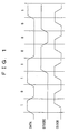
adjacent thereto). Fig. 3A is a diagram showing a network constituted by leaf nodes and branch nodes.
  • At the tree identification phase, the entire network topology is converted into one tree where one node is designated as a route. All the physical connections connected to the route indicate the direction of route node. Each connected port is assigned with a label to indicate the direction, and is referred to as a "parent" port (in the case where the port is connected to the node close to the route), or a "child" port (in the case where the port is connected to the node remote from the route). The port which is not connected to any node is assigned with a label "off", and does not participate in the arbitration process conducted afterwards. Fig. 3B shows the network constituted at the completion of the tree identification process.
  • At the self-identification phase, each node is provided with an opportunity to select its own specific physical_ID to identify itself with respect to an arbitrary control element associated with the bus. This process is also necessary to control electric power of low level, and to produce a topology map of the system required for determining the rate of each data path.
  • The self-identification process employs a decision theoretic selection process. Specifically, a root node leaves the media control to the node associated with the connection port having the smallest number, and waits until the node sends the "ident_done" signal for notifying that the node itself and all the child nodes thereof have completed self-identification. After that, the root node leaves the control to the node associated with the upper port having the next number, and waits until the processing of the node is completed. When the nodes associated with all the ports of the root complete their processings, the root itself conducts self-identification. The child node conducts the same process as above recursively. The completion of the self-identification process is acknowledged when the bus goes into an idle state over a subaction gap period.
  • Each node can send its self-identification information by sending one to four very short packets (Self-ID Packet) involving physical_ID or other control information to a cable. The physical_ID is a value obtained by simply counting the number of times the node which is in the state of receiving the self-identification information is passed before the node sends the self-identification packet. For example, the node which sends its self-identification packet first selects a 0 as a physical_ID, and the node which sends its self-identification packet second selects a 1 as a physical_ID. Same process is repeated to determine the physical_ID of the nodes which send their self-identification packet third and thereafter. Fig. 3C shows the network obtained at the completion of the self-identification process. Each "child" port is assigned with a "ch-i" label by which the node connected to the port can be identified.
  • In the IEEE 1394-1995 and 1394a definition, the behavior of the physical layer at the time when it receives a signal for canceling a request at an arbitration phase is defined as follows: "when a child node which is making a request cancels the request, the physical layer (PHY) at the permission side observes its TX_GRANT signal to be returned thereto as a RX_REQUEST_CANCEL signal [Z0], and returns its state to idle state" (The transition of A1:A0 and transition of A2:A0 in Fig. 4). Fig. 4 is a transition diagram at an arbitration phase, showing a A0 (Idle) state, a A1 (Request) state, a A2 (Grand) state, a RX (Receive) state, a TX (Transmit) state, and PH (PHY Response) state, respectively.
  • However, as shown in Table 5 above, since the RX_GRANT signal [00] and the RX_SUSPEND signal [00] use an identical code, a problem arises in the above operation depending on the way that the physical layer is mounted. That is, although the physical layer is in the state of receiving the RX_GRANT signal from the parent node, when it observes the RX_REQUEST_CANCEL signal from the child node and changes its state into the idle state, the physical layer misunderstands the RX_GRANT signal from the parent node as the RX_SUSPEND signal. As a result, a situation may arise that the port connected to the parent node changes its state into a suspended state. Fig. 5 is a transition diagram at a port connection, showing P0 state (Disconnected), P1 state (Resuming), P2 state (Active), P3 state (Suspended Initiator), P4 state (Suspended Target), P5 state (Suspended), and P6 state (Disabled), respectively.
  • Hereinafter, description will be made on the behavior of a node B at the time when a node A makes a request for obtaining a right to use bus for transmission, and after that, the node A cancels the request, taking as an example the case where 5 nodes are connected to each other where a node C is a route node as shown in Fig. 6A. In Figs. 6A to 9C, arrows show transmission and receipt of data, and the terms IDLE, REQ, GRANT, RECEIVE, and TRANS in the respective nodes show the states of physical layers of the respective nodes. The diagonally shaded arrow shows a request signal and a grant signal (same signals are allocated in the IEEE 1394-1995 and 1394a standard), the grid-patterned arrow shows a data prefix signal, and the filled-in arrow shows a data payload.
  • First, a flow from (1.1) to (1.8) will be described as a normal flow of data transmission from a point where the node A makes a request to obtain a right to use bus for transmission until a point where the node A transmits data.
  • (1.1) In order to obtain the right to use bus for transmission, the node A changes its state into a request state where the node A transmits a request signal (Fig. 6A).
  • (1.2) Upon receiving the request signal from the node A, the node B changes its state into a request state where the node B repeats the request signal to the node C which is a parent node (Fig. 6B).
  • (1.3) Upon receiving the request signal from the node B, the node C confirms that there is no other request signal than that from the node B, and changes its state into a grant state where the node C transmits a grant signal to the node B. At the same time, the node C transmits a data prefix to the other node, that is, the node E. Upon receiving the data prefix signal, the node E changes its state into a receive state (Fig. 6C).
  • (1.4) Upon receiving the grant signal, the node B changes its state into a grant state where the node B repeats the grant signal to the node A. At the same time, the node B transmits a data prefix signal to the other node, that is, the node D. Upon receiving the data prefix signal, the node D changes its state into a receive state (Fig. 6D).
  • (1.5) Upon receiving the grant signal, the node A has obtained the right to use bus for transmission. The node A therefore changes its state into a transmission state where the node A switches the request signal to the data prefix signal (Fig. 7A).
  • (1.6) Upon receiving the data prefix signal from the node A, the node B changes its state into a receive state where the node B repeats the data prefix signal to the nodes C, D. Upon receiving the data prefix signal from the node B, the node C changes its state into the receive state where the node C repeats the data prefix signal to the node E (Fig. 7B).
  • (1.7) After the node A keeps the data prefix signal for a period of time defined by the IEEE 1394 standard, the node A starts to transmit the data payload to the node B (Fig. 7C).
  • (1.8) Upon receiving the data payload from the node A, the node B repeats the data payload to the nodes C and D. Furthermore, upon receiving the data payload from the node B, the node C repeats the data payload to the node E (Fig. 7D).
  • Next, a flow from (2.1) to (2.3) will be described, where the node B receives an idle signal from the node A after the step (1.2) in the above-described flow has completed and during when the node B is transmitting the request signal to the node C.
  • (2.1) In the state where the node B repeats the request signal to the node C and waits to receive a grant signal from the node C, if the node cancels the request for any reason, the node B receives an idle signal from the node A (Fig. 8A).
  • (2.2) Upon receiving the idle signal from the node A, the node B returns its state into an idle state (Fig. 8B).
  • (2.3) If the node B, after returning its state into the idle state, receives a grant signal [Z0] already transmitted from the node C before the request signal [Z0] to the node C is cancelled, the node B misunderstands that it has received a suspend signal [00] (the [00]signal received in the idle state is understood as a suspend signal), although it actually is the grant signal [Z0]. In this case, the node B erroneously changes its state into a suspend state, resulting in occurrence of troubles (Fig. 8C).
  • Next, a flow from (3.1) to (3.3) will be described, where the node B receives a request cancel signal from the node A after the step (1.4) has completed in the above-described flow and during when the node B is receiving the grant signal from the node C.
  • (3.1) In the state where the node B repeats the request signal to the node C, and receives the grant signal from the node C, if the node A cancels a request for any reason, the node B receives a request cancel signal from the node A (Fig. 9A).
  • (3.2) Upon receiving the request cancel signal from the node A, the node B returns its state into an idle state (Fig. 9B).
  • (3.3) The node B, after returning to the idle state, is in the state where it is transmitting a request signal [Z0] to the node C and also is receiving a grant signal [Z0] from the node C. In this state, the node B misunderstands that it has received a suspend signal [00] (the [00]signal received in the idle state is understood as a suspend signal). As a result, the node B erroneously changes its state into a suspend state, resulting in occurrence of troubles (Fig. 9C).
  • Various respective aspects and features of the invention are defined in the appended claims.
  • Embodiments of the present invention relate to electronic equipment in which the physical layer circuit is operated in such a manner that, when receiving a first signal from a child node, the physical layer circuit changes its state from a first state into a second state and sends a first signal to a parent node, and when receiving a third signal for canceling the first signal from the child node before receiving the second signal corresponding to the first signal from the parent node, the physical layer circuit sends the third signal to the parent node after receiving the second signal from the parent node, and furthermore, the physical layer circuit returns its state from the second state to the first state after receiving the third signal from the parent node, thereby avoiding the occurrence of troubles which may be caused if the physical layer circuit receives the second signal from the parent node in the first state.
  • Embodiments of the present invention also relate to electronic equipment in which the physical layer circuit is operated in such a manner that, when receiving a first signal from a child node, the physical layer circuit changes its state from a first state into a second state and sends the first signal to a parent node, and when receiving a third signal for canceling the first signal from the child node after receiving the second signal corresponding to the first signal from the parent node and shifting its state from the second state to the third state, the physical layer circuit sends the third signal to the parent node, and furthermore, the physical layer circuit returns its state from the third state to the first state after receiving the third signal from the parent node, thereby avoiding the occurrence of troubles which may be caused if the physical layer circuit receives the second signal from the parent node in the first state.
  • Embodiments of the present invention can provide electronic equipment capable of preventing the occurrence of troubles such as described above, and a method for controlling the state of the physical layer circuit thereof.
  • In an aspect of the present invention, electronic equipment comprising a physical layer circuit, and a processor upper than the physical layer circuit, wherein the physical layer circuit includes: a first transmitter for performing communication with a child node; a second transmitter for performing communication with a parent node; and a controller for controlling the physical layer circuit in such a manner that, when receiving a first signal from the child node by use of the first transmitter, the physical layer circuit changes its state from a first state into a second state and transmits the first signal to the parent node by use of the second transmitter, for controlling the physical layer circuit in such a manner that, when receiving a third signal for canceling the first signal from the child node by use of the first transmitter before receiving a second signal corresponding to the first signal from the parent node by use of the second transmitter, the physical layer circuit transmits the third signal to the parent node by use of the second transmitter after receiving the second signal from the parent node by use of the second transmitter, and for controlling the physical layer circuit in such a manner that, after receiving the third signal from the parent node by use of the second transmitter, the physical layer circuit returns its state from the second state into the first state.
  • For example, the physical layer circuit constitutes a physical layer which conforms to the IEEE 1394 standard. The first state is an idle state, and the second state is a request state. The first signal is a request signal for obtaining right to use bus for transmission, and the second signal is a grant signal, and the third signal is an idle signal.
  • In another aspect of the present invention, a method for controlling a state of a physical layer circuit including transmitters for performing communication with a child node and a parent node respectively, includes the steps of: when receiving a first signal from a child node, controlling the physical layer circuit to change its state from a first state into a second state, and to transmit the first signal to the parent node; when receiving a third signal for canceling the first signal from the child node before receiving a second signal corresponding to the first signal from the parent node, controlling the physical layer circuit to transmit the third signal to the parent node after receiving the second signal from the parent node; and controlling the physical layer circuit to return its state from the second state to the first state after receiving the third signal from the parent node.
  • In the present invention, the physical layer circuit is free from the situation in which it receives a second signal from the parent node in the first state. This arrangement serves to prevent the occurrence of troubles which may cause if the physical layer circuit receives the second signal from the parent node in the first state. For example, when the physical layer circuit constitutes a physical layer which conforms to the IEEE 1394 standard, if the physical layer circuit receives an idle signal for canceling a request signal from a child node in a request state, the physical layer circuit returns its state into an idle state after it has received an idle signal from the parent node. There arises no situation in which the physical layer circuit receives a grant signal [00] from the parent node in the idle state. This arrangement serves to prevent the occurrence of trouble that the physical layer circuit misunderstands that it has received a suspend signal and changes its state into a suspend state.
  • In still another aspect of the present invention, electronic equipment comprising a physical layer circuit, and a processor upper than the physical layer circuit, wherein the physical layer circuit includes: a first transmitter for performing communication with a child node; a second transmitter for performing communication with a parent node; and a controller for controlling the physical layer circuit in such a manner that, when receiving a first signal from the child node by use of the first transmitter, the physical layer circuit changes its state from a first state into a second state and transmits the first signal to the parent node by use of the second transmitter, for controlling the physical layer circuit in such a manner that, when receiving a third signal for canceling the first signal from the child node by use of the first transmitter after receiving a second signal corresponding to the first signal from the parent node by use of the second transmitter and changing its state from the second state into the third state, the physical layer circuit transmits the third signal to the parent node by use of the second transmitter; and for controlling the physical layer circuit in such a manner that, after receiving the third signal from the parent node by use of the second transmitter, the physical layer circuit returns its state from the third state into the first state.
  • For example, the physical layer circuit constitutes a physical layer which conforms to the IEEE 1394 standard. The first state is an idle state, the second state is a request state, and the third state is a grant state. The first signal is a request signal for obtaining right to use bus for transmission, and the second signal is a grant signal, and the third signal is an idle signal.
  • A method for controlling a state of a physical layer circuit according to the present invention is a method for controlling a state of a physical layer circuit including transmitters for performing communication with a child node and a parent node respectively. When receiving a first signal from a child node, the physical layer circuit is controlled to change its state from a first state into a second state, and to transmit the first signal to the parent node. When receiving a third signal for canceling the first signal from the child node after receiving a second signal corresponding to the first signal from the parent node and changing its state from the second state to the third state, the physical layer circuit is controlled to transmit the third signal to the parent node. The physical layer circuit is controlled to return its state from the third state to the first state after receiving the third signal from the parent node.
  • In the present invention, the physical layer circuit is free from the problem that it receives a second signal from the parent node in the first state. This arrangement serves to prevent the occurrence of trouble which may cause if the physical layer circuit receives the second signal from the parent node in the first state. For example, when the physical layer circuit constitutes a physical layer which conforms to the IEEE 1394 standard, if the physical layer circuit receives an idle signal for canceling a request signal from a child node in a grant state, the physical layer circuit returns its state into an idle state after it has received an idle signal from the parent node. There arises no situation in which the physical layer circuit receives a grant signal [00] from the parent node in the idle state. This arrangement serves to prevent the trouble that the physical layer circuit misunderstands that it has received a suspend signal, although it actually is a grant signal, and changes its state into a suspend state.
  • The invention will now be described by way of example with reference to the accompanying drawings, throughout which like parts are referred to by like references, and in which:
  • Fig. 1 is a diagram showing a structure of transmission data in compliance with the IEEE 1394 standard;
  • Fig. 2 is a cross-sectional view of a cable defined by the IEEE 1394 standard;
  • Figs. 3A to 3C are diagrams showing a network constituted at the completion of bus initialization, tree identification, and self-identification;
  • Fig. 4 is a transition diagram at an arbitration phase;
  • Fig. 5 is a transition diagram at a port connection;
  • Figs. 6A to 6D are diagrams showing a flow (1/2) of normal data transmission;
  • Figs. 7A to 7D are diagrams showing a flow (2/2) of normal data transmission;
  • Figs. 8A to 8C are diagrams showing a flow in the case where a node B receives an idle signal from a node A in a request state;
  • Figs. 9A to 9C are diagrams showing a flow in the case where a node B receives a request cancel signal from a node A in a grant state;
  • Fig. 10 is a block diagram showing an exemplary structure of a network constituted in compliance with the IEEE 1394 standard;
  • Fig. 11 is a diagram showing constituent elements of an interface in compliance with the IEEE 1394 standard, and a protocol architecture;
  • Fig. 12 is a diagram showing a packet in asynchronous transmission;
  • Figs. 13A and 13B are diagrams for illustrating arbitration;
  • Fig. 14 is a diagram showing a packet in isochronous transmission;
  • Fig. 15 is a diagram showing address designation in a CSR architecture;
  • Fig. 16 is an explanatory diagram showing exemplary position, name, and operation of the main CRS;
  • Fig. 17 is an explanatory diagram showing an exemplary general ROM format;
  • Fig. 18 is an explanatory diagram showing exemplary bus info block, root directory, and unit directory;
  • Fig. 19 is an explanatory diagram showing an exemplary structure of PCR;
  • Figs. 20A to 20D are explanatory diagrams showing exemplary structures of oMPR, oPCR, iMPR, and iPCR, respectively;
  • Fig. 21 is an explanatory diagram showing an exemplary relationship between a plug, a plug control register, and a transmission channel;
  • Fig. 22 is an explanatory diagram showing an exemplary data structure in a hierarchy of a descriptor;
  • Fig. 23 is an explanatory diagram showing an exemplary data format of a descriptor;
  • Fig. 24 is an explanatory diagram showing an exemplary generation ID of Fig. 23;
  • Fig. 25 is an explanatory diagram showing an exemplary list ID of Fig. 23;
  • Fig. 26 is an explanatory diagram showing a relationship between the command and the response of FCP;
  • Fig. 27 is an explanatory diagram showing the relationship between the command and the response of Fig. 26 in more detail;
  • Fig. 28 is an explanatory diagram showing an exemplary data structure of an AV/C command;
  • Figs. 29A to 29C are explanatory diagrams showing specific examples of the AV/C command;
  • Figs. 30A and 30B are explanatory diagrams showing specific examples of the command and the response of the AV/C command;
  • Fig. 31 is a block diagram showing an exemplary structure of a physical layer;
  • Fig. 32 is a transition diagram at an arbitration phase;
  • Figs. 33A to 33D are diagrams showing a flow in the case where a node B receives an idle state from a node A in a request state; and
  • Figs. 34A to 34C are diagrams showing a flow in the case where a node B receives a request cancel signal from a node A in a grant state.
  • Hereinafter, embodiments of the present invention will be described in detail with reference to the drawings.
  • Fig. 10 is a diagram showing an exemplary structure of a network constituted based on the IEEE 1394 standard. A work station 10, a personal computer 11, a hard disc drive 12, a CD-ROM drive 13, a camera 14, a printer 15, and a scanner 16 together constitute an IEEE 1394 node, and are connected to each other via IEEE 1394 buses 20. The connection methods in conformity with the IEEE 1394 standard are categorized into two: a daisy chain connection and a node multipoint connection. In the daisy chain connection method, 16 nodes (i.e. equipment having an IEEE 1394 port) can be connected at maximum. As shown in Fig. 10, in combination with the daisy chain connection method and the node multipoint connection method, 63 nodes, which is the maximum number in the IEEE 1394 standard, can be connected.
  • The IEEE 1394 standard allows the cable connection/disconnection in the state where equipment operates, that is, the equipment is turned on. At the time when the node is added or deleted, the reconfiguration of the topology is conducted through the bus initialization phase, the tree identification phase, and the self-identification phase in this order, as described above. The identification and arrangement of the nodes connected to the network is controlled on the interface.
  • Fig. 11 is a diagram showing the constituent elements and the protocol architecture of the interface which conforms to the IEEE 1394 standard. The interface is constituted by hardware and firmware.
  • The hardware is constituted by a physical layer (PHY) and a link layer. The physical layer directly drives a signal which conforms to the IEEE 1394 standard. The link layer includes a host interface and a physical layer interface.
  • The firmware is constituted by a transaction layer and a management layer. The transaction layer is constituted by a management driver for performing an actual operation for the interface which conforms to the IEEE 1394 standard. The management layer is constituted by a driver for managing a network, and is referred to as a serial bus management (SBM) and conforms to the IEEE 1394 standard.
  • The application layer is constituted by a software used by a user, and a management software for interfacing the transaction layer and the management layer.
  • In the IEEE 1394 standard, the transmission operation performed within the network is referred to as a subaction, and the following two subactions are defined. One of the subactions is in a non-synchronous transmission mode referred to as an "asynchronous" mode, while the other is in a real-time transmission mode referred to as an "isochronous" mode in which the transmission band is secured. Each of the subactions is further categorized in the three parts which assume the following states, respectively:
  • An arbitration state;
  • A packet transmission state; and
  • An acknowledgement state,
  •    wherein the acknowledgement state is omitted from the "isochronous" mode.
  • In the subaction in the asynchronous mode, non-synchronous transmission is conducted. Fig. 12 is a diagram showing the transaction state with the lapse of time in the asynchronous transmission mode. In Fig. 12, the initial subaction gap shows that the bus is in the idle state. The time during which the subaction gap lasts is monitored to judge whether or not the immediately preceding transmission has finished and another new transmission is possible.
  • If the idle state lasts for a specified period of time or longer, the node which wishes to conduct transmission judges that the bus is usable, and performs an arbitration for obtaining the bus. In an actual operation, the judgment whether or not to stop the bus is conducted by the node A located at the root, as shown in Figs. 13A and 13B. After the node wishing the transmission obtains the right to use the bus in this arbitration, the node conducts transmission of the next data, that is, packet transmission. After the data transmission, the node which has received the data conducts acknowledgement in response to the data transmission by returning a data receipt acknowledgement return code (ack).
  • By the execution of the acknowledgement, it can be acknowledged from the data receipt acknowledgement return code (ack) that the transmission has normally conducted in both the transmission node and the receiving node.
  • After that, the state is returned to the subaction gap, that is, to the bus idle state again, and the transmission operation as described above is repeated.
  • In the subaction in the isochronous mode, the transmission basically in the same structure as of the transmission in the asynchronous mode is executed, except that, as shown in Fig. 14, the transmission in the isochronous subaction is assigned with higher priority and is executed prior to the transmission in the asynchronous subaction. The isochronous transmission in the isochronous subaction is executed subsequent to the cycle start packet which is issued at every about 8 kHz (125µs), and is assigned with higher priority to be executed prior to the asynchronous transmission in the asynchronous subaction. In this manner, the isochronous transmission is in the transmission mode in which the transmission band is secured, thereby attaining the transmission of the real-time data.
  • The cycle described above is created by the cycle start packet supplied from the node having a cycle master function (i.e. any equipment connected to the bus). In the isochronous transmission, the band required for data transmission (although this is a unit of time, it is referred to as a band) is secured from all the foremost end of the cycle. Therefore, in the isochronous transmission, the data transmission is secured for a specified period of time. However, since the isochronous transmission has no arrangement for data protection, the data is lost when transmission error occurs. On the other hand, in the asynchronous transmission, the node which has obtained the right to use the bus as a result of arbitration during the time when the bus is not used for isochronous transmission in each cycle sends the asynchronous packet. The reliable transmission is possible by employment of the acknowledgement and retry; however, the transmission is not executed at a constant timing.
  • In the plurality of nodes execute real-time data transmission through isochronous transmission, the transmission data is provided with a channel ID for identifying its content (i.e. transmission node), so that only the require real-time data is received.
  • In order to allow a predetermined node to execute isochronous transmission, it is required that the node has the isochronous function. In addition, at least one of nodes having the isochronous function must have also cycle master function. Furthermore, at least one of nodes connected to the IEEE 1394 serial bus must have isochronous resource managing function.
  • The address space defined in the IEEE 1394 standard has a structure such as shown in Fig. 15. This structure conforms to the CSR architecture defined by the ISO/IEC13213 standard for 64-bit fixed addressing (hereinafter, referred to as a "CSR architecture"). As shown in Fig. 12, the upper 16 bits in each address indicate a node ID for providing an address space to the node. The node ID designates the bus ID by its upper 10 bits, and designates the physical ID (i.e. the node ID in a narrow meaning) by its lower 6 bits. The bus ID and the physical ID use a value obtained when all bits are set to 1 for a special purpose. Therefore, this addressing method provides 1023 buses and nodes each capable of designating 63 individual addresses.
  • Among the address space with 256 terabyte defined by the lower 48 bits, the space defined by the upper 20 bits is divided into an initial register space which is used for the register specific to 2048 byte CSR and the register specific to the IEEE 1394 standard, a private space, and an initial memory space. The space defined by the lower 28 bits is used, when the space defined by the upper 20 bits is an initial register space, as a configuration read only memory (ROM), an initial unit space for use specific to the node, a plug control register (PCRs), or the like.
  • Fig. 16 is a diagram for illustrating an offset address, name, and operation of the main CSR. The term "offset" in Fig. 16 shows the offset address close to the FFFFF000000h address (the h at the rearmost end indicates that the address is in a hexadecimal notation) from which the initial register space begins. The bandwidth available register having an offset 220h shows a bandwidth which can be allocated to the isochronous transmission, and recognizes only the value of the node activating as an isochronous resource manager to be effective. Specifically, each node has the CSR shown in Fig. 15, whereas only the bandwidth available register of the isochronous resource manager is recognized to be effective. In other words, it is only the isochronous resource manager that actually has the bandwidth available register. In the bandwidth available register, a maximum value is stored when no bandwidth is allocated to the isochronous transmission, and the value thereof is reduced every time when a bandwidth is allocated to the isochronous transmission.
  • The channels available registers from offset 224h to 228h correspond to the channel numbers with 0 to 63 bits, respectively. In the case where the channel number with 0 bit, it means that the channel has been already allocated to the channels available register. Only the channel available register of the node activating as an isochronous resource manager is effective.
  • Referring again to Fig. 15, a configuration read only memory (ROM) based on the general read only memory (ROM) format is arranged in the addresses 200h to 400h within the initial unit space. Fig. 17 is a diagram for illustrating the general ROM format. The node, which is a unit of access on the IEEE 1394 standard, can hold a plurality of units capable of independently operate while having the common address space in the node. The unit directories can indicate the version and the position of the software for the unit. The bus info block and the root directory are located at fixed positions, and the other blocks are located at positions designated by the offset address.
  • Fig. 18 is a diagram showing bus info block, root directory, and unit directory in detail. An ID number for indicating the manufacturer of the equipment is stored in the company ID in the bus info block. An ID which is specific to the equipment and is the only one ID in the world without overlapping other IDs is stored in the chip ID. 00h is written into the first octet of the unit spec ID of the unit directory of the equipment satisfying the requirements of the IEC 61883 standard, and Aoh is written into the second octet thereof, and 2Dh is written into the third octet thereof, respectively. Furthermore, 01h is written in the first octet of the unit switch version, and 1 is written into the least significant bit (LSB) of the third octet.
  • The node has a plug control register (PCR) defined by the IEC61883 standard in the addresses 900h to 9FFh within the initial unit space shown in Fig. 15, in order to control an input/output of the equipment via the interface. This design embodies the concept of plug to form a signal path logically similar to an analog interface. Fig. 19 is a diagram for illustrating the structure of PCR. The PCR has an output plug control register (oPCR) indicating an output plug, and an input plug control register (iPCR) indicating an input plug. The PCR also has an output master plug register (oMPR) or an input master plug register (iMPR) for indicating information on the output plug or the input plug specific to each device. Each device does not have a plurality of oMPR nor iMPR, but may have, in accordance with its ability, a plurality of oPCR or iPCR corresponding to each plug thereof. Each of the PCRs shown in Figs. 20A to 20D have 31 oPCRs and 31 iPCRs. The isochronous data flow is controlled by manipulating the registers corresponding to these plugs.
  • Figs. 20A to 20D are diagrams showing structures of oMPR, oPCR, iMPR, and iPCR, respectively. Fig. 20A shows the structure of oMPR, Fig. 20B shows the structure of oPCR, Fig. 20C shows the structure of iMPR, and Fig. 20D shows the structure of iPCR, respectively. A code indicating the maximum transmission rate of the isochronous data which the device can send or receive is stored in the data rate capability with 2 bits at the MSB side in each of the oMPR and iMPR. A broadcast channel base in the oMPR defines the channel number to be used for broadcast output.
  • The number of output plugs that the device has, that is, the value showing the number of oPCRs is stored in the number of output plugs with 5 bits at the LSB side in the oMPR. The number of input plugs that the device has, that is, the value showing the number of iPCR is stored in the number of input plugs with 5 bits at the LSB side in the iMPR. A non-persistent extension field and a persistent extension field are regions prepared for future expansion.
  • An on-line at the MSB in each of the oPCR and iPCR indicates the use state of the plug. Specifically, the value at 1 on the on-line means that the plug is in an on-line state, and the value at 0 on the on-line means that the plus is in an off-line state. The values on the broadcast connection counter of each of the oPCR and iPCR indicates the presence (the value at 1) or absence (the value at 0) of the broadcast connection. The value on the point-to-point connection counter with 6-bit width in each of the oPCR and iPCR indicates the number of the point-to-point connections that the plug has.
  • The value on the channel number with 6-bit width in each of the oPCR and iPCR indicates the isochronous channel number to which the plug is to be connected. The value on the data rate with 2-bit width in oPCR indicates an actual transmission rate of the packet of the isochronous data to be output from the plug. The code stored in the overhead ID with 4-bit width in the oPCR shows the bandwidth over the isochronous communication. The value on the payload with 10-bit width in the oPCR indicates the maximum value of the data involved in the isochronous packet that can be handled by the plug.
  • Fig. 21 is a diagram showing the relationship between the plug, the plug control register, and the isochronous channel. AV-devices 71 to 73 are connected with each other by IEEE 1394 serial bus. The oMPR in the AV device 73 defines the number and the transmission rate of the oPCR[0] to oPCR[2]. The isochronous data for which the channel is designated by the oPCR [1] among the oPCR [0] to oPCR[2] is sent to the channel #1 in the IEEE 1394 serial bus. The iMPR in the AV device 71 defines the number and transmission rate of iPCR[0] and iPCR[1]. The AV device 71 read the isochronous data which has been sent to the channel #1 in the IEEE 1394 serial bus which is designated by the iPCR[0] between the iPCR[0] and iPCR[1]. Similarly, the AV device 72 sends the isochronous data to the channel #2 designated by the oPCR[0]. The AV device 71 reads the isochronous data from the channel #2 designated by the iPCR[1].
  • In the aforementioned manner, data transmission is executed between the devices connected to each other by the IEEE 1394 serial bus. In this structure, each device can be controlled and the state thereof can be acknowledged by use of an AV/C command set defined as a command for controlling the devices connected to each other by the IEEE 1394 serial bus. Hereinafter, the AV/C command set will be described.
  • First, description will be made on a data structure of the subunit identifier descriptor in the AV/C command set, referring to Figs. 22 to 25. Fig. 22 is a diagram showing a data structure of the subunit identifier descriptor. As seen in Fig. 22, the data structure of the subunit identifier descriptor is constituted by hierarchical lists. The term "list" means, in the case of a tuner for example, a channel through which data can be received, and means, in the case of a disc for example, a music recorded therein. The uppermost list in the hierarchy is referred to as a root list, and a list 0 is a root for the lists at lower positions for example. Similarly, the lists 2 to (n-1) are also root lists. The root lists exist in the same numbers as of the objects. The term "object" means, in the case where the AV device is a tuner, each channel in a digital broadcasting. All the lists in one hierarchy share the same information.
  • Fig. 23 is a diagram showing a format of the general subunit identifier descriptor. The subunit identifier descriptor 41 has contents including attribute information as to the functions. No value of the descriptor length field itself is involved in the contents. The generation ID indicates the AV/C command set version, and its value is at "00h" (the h designates that this value is in hexadecimal notation) at present as shown in Fig. 24. The value at "00h" means that the data structure and the command are of AV/C general specification, version 3.0. In addition, as shown in Fig. 24, all the values except for "00h" are stored in reserved states for future specification.
  • The size of list ID shows the number of bytes of the list ID. The size of object ID shows the number of bytes of the object ID. The size of object position shows the position (i.e. the number of bytes) in the lists to be referred in a control operation. The number of root object lists show the number of root object lists. The root object list ID shows an ID for identifying the uppermost root object list in the independent layers in the hierarchy.
  • The subunit dependent length means the number of bytes of the subsequent subunit dependent information field. The subunit dependent information is a field showing information specific to the functions. The manufacturer dependent length shows the number of bytes of the subsequent manufacturer dependent information field. The manufacturer dependent information is a field showing information about the specification determined by the vender (i.e. manufacturer). When the descriptor has no manufacturer dependent information, the manufacturer dependent information field does not exist.
  • Fig. 25 is a diagram showing the list ID assignment ranges shown in Fig. 23. As shown in Fig. 25, the values at "0000h to OFFFh" and "4000n to FFFFh" are stored in reserved states for future specification. The values at "1000h to 3FFFh""and "10000h to max list ID value" are prepared for identifying dependent information about function type.
  • Next, the AV/C command set will be described with reference to Figs. 26 to 30B.
  • Fig. 26 is a diagram for illustrating the command and the response of an FCP 85 of Fig. 27. The FCP is a protocol for controlling the AV device in conformity to the IEEE 1394 standard. As shown in Fig. 26, a controller is a control side, and a target is a side to be controlled. In the FCP, the command is transmitted and received between nodes by use of the write transaction in the IEEE 1394 asynchronous transmission. Upon receiving data from the controller, the target returns an acknowledgement to the controller for notifying that it has received the data.
  • Fig. 27 is a diagram for further illustrating the relationship between the command and the response of FCP shown in Fig. 26. A node A is connected with a node B via an IEEE 1394 bus. The node A is a controller, and the node B is a target. Each of the nodes A and B is provided with a command register and a response register each with 512 bytes. As shown in Fig. 27, the controller writes a command massage into a command register 93 in the target to give command thereto. Contrarily, the target writes a response message into a response register 92 in the controller to give response thereto. Between these two messages, control information is exchanged. The kind of the command set sent in the FCP is written in the CTS in the data field shown in Fig. 28 which will be described later.
  • Fig. 28 is a diagram showing a data structure of a packet of the AV/C command to be transmitted in the asynchronous transmission. The AV/C command set is a command set for controlling the AV device where CTS (i.e. a command set ID) = "0000". The AV/C command frame and the response frame are exchanged between nodes by use of the FCP described above. In order to prevent burdening the bus and the AV device, the time for the response to the command is limited within 100ms. As shown in Fig. 28, the asynchronous packet data is constituted by 32 bits in a horizontal direction (i.e. quadlet). A header of the packet is shown in the upper half portion of Fig. 28, and a data block is shown in the lower half portion of Fig. 28. The destination_ID shows an address.
  • The CTS shows the command set ID, wherein CTS="0000" in the AV/C command set. The ctype/response field shows the function sort of the command when the packet is a command, while shows the result of command processing when the packet is a response. The command is roughly classified into four categories as follows: (1) a command for controlling the function from the outside (CONTROL); (2) a command for inquiring the state from the outside (STATUS); (3) a command for inquiring whether or not there is a support for control command from the outside (GENERAL INQUIRY for inquiring whether or not there is a support for opcode, and SPECIFIC INQUIRY for inquiring whether or not there is a support for opcode and operands); and (4) a command for requesting to notify the change in the state to the outside (NOTIFY).
  • What response is returned depends on the kind of the command. The response to the control command is categorized into NOT IMPLEMENTED, ACCEPTED, REJECTED, and INTERIM. The response to the status command is categorized into NOT IMPLEMENTED, REJECTED, IN TRANSITION, and STABLE. The response to the general inquiry command and the specific inquiry command is categorized into IMPLEMENTED and NOT IMPLEMENTED. The response to the notify command is categorized into NOT IMPLEMENTED, REJECTED, INTERIM, and CHANGED.
  • The subunit type is provided to specify the function in the device, and is assigned with a tape recorder/player, tuner, and the like. In order to identify each subunit from the others in the case where a plurality of subunits of the same kind other exist, the subunit type executes addressing by use of a subunit ID as an identification number. The opcode shows a command, and the operand shows a parameter of the command. The additional operands are fields added if necessary. The padding is a field also added if necessary. The data cyclic redundancy check (CRC) is used for error check in data transmission.
  • Figs. 29A to 29C are diagrams showing specific examples of the AV/C command. Fig. 29A shows a specific example of the ctype/response. The upper half portion of Fig. 29A shows command, while the lower half portion of Fig. 29B shows responses. The value at "0000" is assigned with CONTROL, the value at "0001" is assigned with STATUS, the value at "0010" is assigned with SPECIFIC INQUIRY, the value at "0011" is assigned with NOTIFY, and the value at "0100" is assigned with GENERAL INQUIRY. The values at "0101" to "0111" are stored in a reserved state for future specification. In addition, the value at "1000" is assigned with NOT INPLEMENTED, the value at "1001" is assigned with ACCEPTED, the value at "1010" is assigned with REJECTED, the value at "1011" is assigned with IN TRANSITION, the value at "1100" is assigned with IMPLEMENTED/STABLE, the value at "1101" is assigned with CHANGED, and the value at "1111" is assigned with INTERIM. The value at "1110" is stored in a reserved state for future specification.
  • Fig. 29B shows a specific example of the subunit type. The value at "00000" is assigned with a video monitor, the value at "00011" is assigned with a disk recorder/player, the value at "00100" is assigned with a tape recorder/player, the value at "00101" is assigned with a tuner, the value at "00111" is assigned with a video camera, the value at "11100" is assigned with a vendor unique, the value at "11110" is assigned with a subunit type extended to next byte. The value at "11111" is assigned with a unit, and is used for transmitting data to the device itself, for example, for turning on and off the electric power source.
  • Fig. 29C shows a specific example of the opcode. Each subunit type has its own opcode table, and Fig. 29C shows the opcode in the case where the subunit type is a tape recorder/player. In addition, operand is defined for each opcode. In the example of Fig. 29C, the value at "00h" is assigned with VENDOR-DEPENDENT, the value at "50h" is assigned with SEARCH MODE, the value at "51h" is assigned with TIMECODE, the value at "52h" is assigned with ATN, the value at "60h" is assigned with OPEN MIC, the value at "61h" is assigned with READ MIC, the value at "62h" is assigned with WRITE MIC, the value at "C1h" is assigned with LOAD MEDIUM, the value at "C2h" is assigned with RECORD, the value at "C3h" is assigned with PLAY, and the value at "C4h" is assigned with WIND.
  • Figs. 30A and 30B show specific examples of the AV/C command and response. For example, when instruction for executing reproduction is provided to the reproducing device as a target (consumer), the controller sends a command such as shown in Fig. 30A to the target. Since this command uses AV/C command set, the CTS is at the value at "0000". Since the command for controlling the device from the outside (CONTROL) is used for the ctype, the ctype is at the value at "0000" (see Fig. 29A). Since the subunit type is a tape recorder/player, the subunit type is at the value at "00100" (see Fig. 29B). The id shows the case of ID0, wherein the id is at the value of 000. The opcode is at the value of C3h which means reproduction (see Fig. 29C). The operand is at the value of 75h which means FORWARD. When reproduced, the target returns the response such as shown in Fig. 30B to the controller. In the example shown in Fig. 30B, "accepted", meaning that the data has been received enters the response, and therefore, the response is at the value of "1001" (see Fig. 29A). Except for the response, the other configurations of Fig. 30B is basically the same as of Fig. 30A, and therefore, their descriptions will be omitted.
  • The physical layer which conforms to the IEEE 1394 standard described above, as shown in Fig. 31 for example, includes: a physical layer logical block (PHY LOGIC) 102; a selector block (RXCLOCK/DATA SELECTOR) 103; port logical blocks (PORT LOGIC 1, PORT LOGIC 2, and PORT LOGIC 3) 104, 105, and 106; cable ports (CABLE PORT 1, CABLE PORT 2, CABLE PORT 3) 107, 108, and 109; and a clock generation block (PLL) 110.
  • The physical layer logical block 102 executes input-output (I/O) control and arbitration control between the physical layer and the link layer defined by the IEEE 1394 standard. The physical layer logical block 102 is connected to a link layer controller 100, and also connected to the selector block 103, and each of the port logical blocks 104, 105, and 106.
  • The selector block 103 selects one pair from: data DATA 1 which it receives via the logical block 104 connected to the cable port 107, and a receive clock RXCLK 1 thereof; data DATA 2 which it receives via the logical block 105 connected to the cable port 108, and a receive clock RXCLK 2 thereof; and data DATA 3 which it receives via the logical block 106 connected to the cable port 109, and a receive clock RXCLK 3 thereof. The selector block 103 is connected to the physical layer block 102 and each of the port logical blocks 104, 105, and 106.
  • In transmitting data, the selector block 102 transmits packet data DATA, which has been sent from the physical layer logical block 102, to all the port logical blocks 104, 105, and 106. In receiving data, the selector block 103 selects one pair from: packet data DATA 1 which it receives via the port logical block 104, and a receive clock RXCLK 1 thereof; packet data DATA 2 which it receives via the port logical block 105, and a receive clock RXCLK 2 thereof; and packet data DATA 3 which it receives via the port logical block 106, and a receive clock RXCLK 3 thereof. The selector block 103 then sends the selected pair, for example, the packet data DATA 1 which it has received via the port logical block 104 through the cable port 107, and the receive clock RXCLK 1 thereof, to the physical layer logical block 102. The packet data selected by the selector block 103, for example, the packet data DATA 1 received via the port logical block 104, is written by the receive clock RXCLK 1 thereof into a FIFO memory within the physical layer logical block 102. The packet data which has been written into the FIFO memory is read by use of a system clock SYSCLK which is provided from the clock generation block 110.
  • The port logical block 104 transmits and receives an arbitration signal ARB 1 and data DATA 1 via the cable port 107, and has a function of producing a receive clock RXCLK 1 from data transmitted via the cable port 107 and a strobe signal thereof. When arbitration is conducted, an arbitration signal ARB 1 is sent to the port logical block 104 from the physical-layer logical block 102.
  • In transmitting data, the port logical block 104 converts a packet data DATA 1 sent from the physical layer logical block 102 via the selector block 103 into serial data by use of a transmission clock TXCLK provided from the clock generation block 110. Then, the port logical block 104 transmits the resultant serial data through the cable port 107.
  • In receiving data, the port logical block 104 transmits the packet data DATA 1, which it has received via the cable port 107, to the physical layer logical block 102 together with the receive clock RXCLK 1 thereof via the selector block 103. In the case where the port logical block 104 is selected by the selector block 103, the packet data DATA 1 is written into the FIFO memory within the physical layer logical block 102 by use of the receive clock RXCLK 1 thereof.
  • The port logical block 105 transmits and receives an arbitration signal ARB 2 and data DATA 2 via the cable port 108, and has a function of producing a receive clock RXCLK 2 from data transmitted via the cable port 108 and a strobe signal thereof. When arbitration is conducted, an arbitration signal ARB 2 is sent to the port logical block 105 from the physical layer block 102.
  • In transmitting data, the port logical block 105 converts packet data DATA 2 sent from the physical layer logical block 102 via the selector block 103 into serial data by use of a transmission clock TXCLK provided from the clock generation block 110. Then, the port logical block 105 transmits the resultant serial data through the cable port 108.
  • In receiving data, the port logical block 105 transmits the packet data DATA 2, which it has received via the cable port 108, to the physical layer logical block 102 together with the receive clock RXCLK 2 thereof via the selector block 103. In the case where the port logical block 105 is selected by the selector block 103, the packet data DATA 2 is written into the FIFO memory within the physical layer logical block 102 by use of the receive clock RXCLK 2 thereof.
  • The port logical block 106 transmits and receives an arbitration signal ARB 3 and data DATA 3 via the cable port 109, and has a function of producing a receive clock RXCLK 3 from data transmitted via the cable port 109 and a strobe signal thereof. When arbitration is conducted, an arbitration signal ARB 3 is sent to the port logical block 106 from the physical layer logical block 102.
  • In transmitting data, the port logical block 106 converts packet data DATA 3 sent from the physical layer logical block 102 via the selector block 103 into serial data by use of a transmission clock TXCLK provided from the clock generation block 110. Then, the port logical block 106 transmits the resultant serial data through the cable port 109.
  • In receiving data, the port logical block 106 transmits the packet data DATA 3, which it has received via the cable port 109, to the physical layer logical block 102 together with the receive clock RXCLK 3 thereof via the selector block 103. In the case where the port logical block 106 is selected by the selector block 103, the packet data DATA 3 is written into the FIFO memory within the physical layer logical block 102 by use of the receive clock RXCLK 3 thereof.
  • The cable port 107 drives a twisted pair cable by use of a signal transmitted from the port logical block 104. In addition, the cable port 107 converts the level of the signal sent thereto via the twisted pair cable, and sends the resultant signal to the port logical block 104.
  • The cable port 108 drives a twisted pair cable by use of a signal transmitted from the port logical block 105. In addition, the cable port 108 converts the level of the signal sent thereto via the twisted pair cable, and sends the resultant signal to the port logical block 105.
  • The cable port 109 drives a twisted pair cable by use of a signal transmitted from the port logical block 105. In addition, the cable port 109 converts the level of the signal sent thereto via the twisted pair cable, and sends the resultant signal to the port logical block 109.
  • The clock generation block 110 generates a 49.152 MHz system clock SYSCLK and a 98.304 MHz transmission clock TXCLK from a 24.576 MHz clock provided form a quartz oscillator 111.
  • In this embodiment, an arbitration phase is performed in accordance with the transition diagram shown in Fig. 32. The transition diagram shown in Fig. 32 additionally includes RC1 (WAITGRANT) state and RC2 (WAITIDLE) state, on top of A0 (Idle) state, A1 (Request) state, A2 (Grant) state, RX (Receive) state, TX (Transmit) state, and PH (PHY Response) state in the transition diagram shown in Fig. 4.
  • In RC1 (WAITGRANT) state, a grant signal from the parent port is waited while keeping the request signal to the port. In RC2 (WAITIDLE) state, an idle signal is transmitted to the parent node, and it is waited that the grant signal from the parent port is changed into an idle signal.
  • The change from A1 (Request) state into RC 1 (WAITGRANT) state is executed under the transition condition of "! child_request ()", meaning that the request signal from the child port has been lost. The change from A2 (Grant) state into RC2 (WAITIDLE) state is executed under the transition condition of "portR (requesting_child)==RX_REQUEST_CANCEL", meaning that a request cancel signal (identical to an idle signal) is received by the child port. In addition, the change from RC 1 (WAITGRANT) state into RC 2 (WAITIDLE) is executed under the transition condition of "portR(parent_port)==RX_GRANT", meaning that a grant signal has been received from the parent port. The change from RC 2 (WAITIDLE) state into A0 (Idle) state is executed under the transition condition of "portR(parent_port)==IDLE", meaning that an idle signal has been received from the parent port.
  • Since the arbitration phase is conducted in accordance with the transition diagram shown in Fig. 32, there arises no situation in which a grant signal [00] is received in an idle state. This arrangement serves to prevent the occurrence of trouble that the grant signal is misunderstood as a suspend signal and the state is erroneously changed into a suspend state.
  • Hereinafter, a flow from (4.1) to (4.4) will be described, taking as an example a case where 5 nodes are connected and the node C among them is a route node. In this example, the node A changes its state into a request state in order to obtain the right to use bus for transmission, and transmits a request signal to the node B (Fig. 6A). Upon receiving the request signal from the node A, the node B changes its state into a request state where the node B repeats the request signal to the node C which is a parent node. During when the node B is transmitting the request signal to the node C (Fig. 6B), the node B receives an idle signal from the node A.
  • (4.1) When the node B receives a request cancel from the node A, the node B changes its state into a wait grant state (i.e. RC1 state in Fig. 32) where the node B waits to receive a grant signal from the node C while keeping the request signal. Upon receiving the request signal, the node C confirms there is no other request signal than that from the node B, and changes its state into a grant state where the node C transmits a grant signal to the node B. At the same time, the node C transmits a data prefix signal to the other node, that is, the node E. Upon receiving the data prefix signal, the node E changes its state into a receive state (Fig. 33A).
  • (4.2) The node B confirms that it has received the grant signal from the node C, and after that, changes its state from the wait grant state into a wait idle state (i.e. RC2 state in Fig. 32) where the node B transmits an idle signal to the node C, and waits until the grant signal from the node C changes into an idle signal (Fig. 33B).
  • (4.3) Since the node C is a route node, the node C receives the idle signal from the node B and returns its state into an idle state where the node C transmits an idle signal to the node B and cancels the data prefix signal to the node E (Fig. 33C).
  • (4.4) The node B confirms that it has received the idle signal from the node C, and after that, returns its state from the wait idle state into an idle state (Fig. 33D).
  • As described above, the node B is designed so that, when the node B receives an idle signal for canceling the request signal from the node A in the request state, the node B returns its state into an idle state after it has received an idle signal from the node C. Therefore, the node B is free from the situation in which it receives a grant signal [00] from the node C in the idle state. This arrangement prevents the node B from misunderstanding that it has received a suspend signal and erroneously changing its state into a suspend state.
  • Hereinafter, a flow from (5.1) to (5.3) will be described, taking as an example a case where 5 nodes are connected and the node C among them is a route node. In this example, the node A changes its state into a request state in order to obtain the right to use bus for transmission, and transmits a request signal (Fig. 6A). Upon receiving the request signal from the node A, the node B changes its state into a request state where the node B repeats the request signal to the node C which is a parent node. The node B transmits the request signal to the node C (Fig. 6B), and the node C confirms that there is no other request signal than that from the node B, and changes its state into a grant state where the node C transmits a grant signal to the node B (Fig. 6C). Upon receiving the grant signal, the node B changes its state into a grant state. During when the node B, after changing its state into the grant state, is repeating the grant signal to the node A (Fig. 6D), the node B receives a request cancel signal (identical to an idle signal) from the node A.
  • (5.1) When the node B receives a request cancel from the node A, the node B changes its state into a wait idle state (i.e. RC2 state in Fig. 32) where the node B transmits an idle signal to the node C and waits that the grant signal from the node C as a parent node changes into an idle signal (Fig. 34A).
  • (5.2) Since the node C is a route node, the node C-receives the idle signal form the node B and returns its state into an idle state where the node C transmits an idle signal to the node B and cancels the data prefix signal to the node E (Fig. 34B).
  • (5.3) The node B confirms that it has received the idle signal from the node C, and after that, cancels the data prefix signal to the node D and returns its state from the wait idle state into an idle state (Fig. 34C).
  • As described above, the node B is designed so that, when the node B receives a request cancel signal (identical to an idle signal) from the node A in the grant state, the node B returns its state into an idle state after it has received an idle signal from the node C. Therefore, the node B is free from the situation in which it receives a grant signal [00] from the node C in the idle state. This arrangement serves to prevent the node B from misunderstanding that it has received a suspend signal and erroneously changing its state into a suspend state.
  • As described above, in this embodiment, when an idle signal for canceling a request signal is received from the child node in a request state, the state is changes into an idle state after an idle signal is received from the parent node. Therefore, there arises no situation in which a grant signal [00] is received from the parent node in an idle state. This arrangement serves to prevent the occurrence of trouble that the grant signal is misunderstood as a suspend signal and the state is erroneously changed into a suspend state.
  • In addition, when a request cancel signal (i.e. an idle signal) is received from the child node in a grant state, the state is changed into an idle state after receiving the idle signal from the parent node. Therefore, there arises no situation in which a grant signal [00] is received from the parent node in an idle state. This arrangement serves to prevent the occurrence of trouble that the grant signal is misunderstood as a suspend signal and the state is erroneously changed into a suspend state.
  • In the above embodiment, the present invention has been described as being applicable to the physical layer circuit constituting the physical layer which conforms to the IEEE 1394 standard, and electronic equipment including the physical layer circuit. However, the present invention is not limited thereto, but may be applicable to other physical layer circuits which have the same problems to be solved as described above.
  • According to the present embodiments, the physical layer circuit is operated in such a manner that, when receiving a first signal from a child node, the physical layer circuit changes its state from a first state to a second state and sends a first signal to a parent node, and when receiving a third signal for canceling the first signal from the child node before receiving a second signal corresponding to the first signal from the parent node, the physical layer circuit sends the third signal to the parent node after receiving the second signal from the parent node, and-furthermore, the physical layer circuit returns its state from the second state to the first state after receiving the third signal from the parent node. In this manner, there arises no situation in which the second signal is received from the parent node in the first state, and thereby avoiding the occurrence of troubles which may be caused if such a situation occurs.
  • In addition, the physical layer circuit is operated in such a manner that, when receiving a first signal from a child node, the physical layer circuit changes its state from a first state to a second state and sends the first signal to a parent node, and when receiving a third signal for canceling the first signal from the child node after receiving a second signal corresponding to the first signal from the parent node and changing its state from the second state to the third state, the physical layer circuit sends the third signal to the parent node, and furthermore, the physical layer circuit returns its state from the third state to the first state after receiving the third signal from the parent node. In this manner, there arises no situation in which the second signal is received from the parent node in the first state, and thereby avoiding the trouble which may be caused if such a situation occur.
  • In so far as the embodiments of the invention described above are implemented, at least in part, using software-controlled data processing apparatus, it will be appreciated that a computer program providing such software control and a storage medium by which such a computer program is stored are envisaged as aspects of the present invention.

Claims (12)

  1. Electronic equipment comprising a physical layer circuit, and a processor upper than the physical layer circuit,
       wherein the physical layer circuit includes:
    a first transmitter for performing communication with a child node;
    a second transmitter for performing communication with a parent node; and
    a controller for controlling the physical layer circuit in such a manner that, when receiving a first signal from the child node by use of the first transmitter, the physical layer circuit changes its state from a first state into a second state and transmits the first signal to the parent node by use of the second transmitter,
    for controlling the physical layer circuit in such a manner that, when receiving a third signal for canceling the first signal from the child node by use of the first transmitter before receiving a second signal corresponding to the first signal from the parent node by use of the second transmitter, the physical layer circuit transmits the third signal to the parent node by use of the second transmitter after receiving the second signal from the parent node by use of the second transmitter, and
    for controlling the physical layer circuit in such a manner that, after receiving the third signal from the parent node by use of the second transmitter, the physical layer circuit returns its state from the second state into the first state.
  2. Electronic equipment according to claim 1,
       wherein the physical layer circuit constitutes a physical layer which conforms to the IEEE 1394 standard.
  3. Electronic equipment according to claim 2,
    wherein the first state is an idle state, and the second state is a request state, and
    wherein the first signal is a request signal for obtaining right to use bus for transmission, and the second signal is a grant signal, and the third signal is an idle signal.
  4. A method for controlling a state of a physical layer circuit including transmitters for performing communication with a child node and a parent node respectively, comprising the steps of:
    when receiving a first signal from a child node, controlling the physical layer circuit to change its state from a first state into a second state, and to transmit the first signal to the parent node;
    when receiving a third signal for canceling the first signal from the child node before receiving a second signal corresponding to the first signal from the parent node, controlling the physical layer circuit to transmit the third signal to the parent node after receiving the second signal from the parent node; and
    controlling the physical layer circuit to return its state from the second state to the first state after receiving the third signal from the parent node.
  5. A method for controlling a state of a physical layer circuit according to claim 4,
       wherein the physical layer circuit constitutes a physical layer which conforms to the IEEE 1394 standard.
  6. A method for controlling a state of a physical layer circuit according to claim 5,
    wherein the first state is an idle state, and the second state is a request state, and
    wherein the first signal is a request signal for obtaining the right to use bus for transmission, and the second signal is a grant signal, and the third signal is an idle signal.
  7. Electronic equipment comprising a physical layer circuit, and a processor upper than the physical layer circuit,
       wherein the physical layer circuit includes:
    a first transmitter for performing communication with a child node;
    a second transmitter for performing communication with a parent node; and
    a controller for controlling the physical layer circuit in such a manner that, when receiving a first signal from the child node by use of the first transmitter, the physical layer circuit changes its state from a first state into a second state and transmits the first signal to the parent node by use of the second transmitter,
    for controlling the physical layer circuit in such a manner that, when receiving a third signal for canceling the first signal from the child node by use of the first transmitter after receiving a second signal corresponding to the first signal from the parent node by use of the second transmitter and changing its state from the second state into the third state, the physical layer circuit transmits the third signal to the parent node by use of the second transmitter; and
    for controlling the physical layer circuit in such a manner that, after receiving the third signal from the parent node by use of the second transmitter, the physical layer circuit returns its state from the third state into the first state.
  8. Electronic equipment according to claim 7,
       wherein the physical layer circuit constitutes a physical layer which conforms to the IEEE 1394 standard.
  9. Electronic equipment according to claim 8,
    wherein the first state is an idle state, the second state is a request state, and the third state is a grant state, and
    wherein the first signal is a request signal for obtaining right to use bus for transmission, and the second signal is a grant signal, and the third signal is an idle signal.
  10. A method for controlling a state of a physical layer circuit including transmitters for performing communication with a Child node and a parent node respectively, comprising the steps of:
    controlling the physical layer circuit in such a manner that, when receiving a first signal from the child node, the physical layer circuit changes its state from a first state into a second state and transmits the first signal to the parent node,
    controlling the physical layer circuit in such a manner that, when receiving a third signal for canceling the first signal from the child node after receiving a second signal corresponding to the first signal from the parent node, and changing its state from the second state into the third state, the physical layer circuit transmits the third signal to the parent node; and
    controlling the physical layer circuit in such a manner that, after receiving the third signal from the parent node, the physical layer circuit returns its state from the third state into the first state.
  11. A method for controlling a state of a physical layer-circuit according to claim 10,
       wherein the physical layer circuit constitutes a physical layer which conforms to the IEEE 1394 standard.
  12. A method for controlling a state of a physical layer circuit according to claim 11,
    wherein the first state is an idle state, the second state is a request state, and the third state is a grant state, and
    wherein the first signal is a request signal for obtaining right to use bus for transmission, and the second signal is a grant signal, and the third signal is an idle signal.
EP01303697A 2000-04-27 2001-04-23 Electronic equipment, and method for controlling state of physical layer circuit thereof Withdrawn EP1150460A1 (en)

Applications Claiming Priority (2)

Application Number Priority Date Filing Date Title
JP2000128127 2000-04-27
JP2000128127A JP2001313646A (en) 2000-04-27 2000-04-27 Electronic device and method for controlling state of its physical layer circuit

Publications (1)

Publication Number Publication Date
EP1150460A1 true EP1150460A1 (en) 2001-10-31

Family

ID=18637615

Family Applications (1)

Application Number Title Priority Date Filing Date
EP01303697A Withdrawn EP1150460A1 (en) 2000-04-27 2001-04-23 Electronic equipment, and method for controlling state of physical layer circuit thereof

Country Status (5)

Country Link
US (1) US6823408B2 (en)
EP (1) EP1150460A1 (en)
JP (1) JP2001313646A (en)
KR (1) KR100746900B1 (en)
TW (1) TW541812B (en)

Cited By (1)

* Cited by examiner, † Cited by third party
Publication number Priority date Publication date Assignee Title
KR100746900B1 (en) * 2000-04-27 2007-08-07 소니 가부시끼 가이샤 Electronic equipment, and method for controlling state of physical layer circuit thereof

Families Citing this family (15)

* Cited by examiner, † Cited by third party
Publication number Priority date Publication date Assignee Title
JP4214346B2 (en) * 2000-07-31 2009-01-28 富士フイルム株式会社 Communication device, server, service providing apparatus, service system and service method, service menu providing method and service menu providing system
JP2002237817A (en) * 2001-02-07 2002-08-23 Nec Eng Ltd Ieee-1394 circuit system
US7130278B1 (en) * 2001-06-25 2006-10-31 Cisco Technology, Inc. Multi-layered cross-sectional diagram of a network
DE10246895B3 (en) * 2002-10-08 2004-06-09 Siemens Ag Procedure for changing a parameter for the operation of a network and participants for performing the procedure
US8836960B1 (en) 2007-01-03 2014-09-16 Marvell International Ltd. Storing device drivers in imaging devices
US8260978B1 (en) 2008-05-28 2012-09-04 Marvell International Ltd. Installation of a device driver
US8244894B1 (en) 2008-06-05 2012-08-14 Marvell International Ltd. Detach mechanisms for host-based mobility protocols
US9354898B1 (en) 2008-07-21 2016-05-31 Marvell International Ltd. Detection of a USB OS descriptor request to facilitate installation of a device driver
JP5729129B2 (en) * 2011-05-24 2015-06-03 富士通セミコンダクター株式会社 COMMUNICATION DEVICE, SEMICONDUCTOR DEVICE, AND DEVICE ID SETTING METHOD
CN104995888B (en) * 2013-02-12 2018-11-16 Nec显示器解决方案株式会社 Electronic equipment and method for controlling electronic devices
US11809163B2 (en) 2019-08-01 2023-11-07 Vulcan Technologies Shanghai Co., Ltd. Intelligent controller and sensor network bus, system and method including a message retransmission mechanism
US11269316B2 (en) 2019-08-01 2022-03-08 Vulcan Technologies Shanghai Co., Ltd. Intelligent controller and sensor network bus, system and method including smart compliant actuator module
US11269795B2 (en) 2019-08-01 2022-03-08 Vulcan Technologies Shanghai Co., Ltd. Intelligent controller and sensor network bus, system and method including a link media expansion and conversion mechanism
US11689386B2 (en) 2019-08-01 2023-06-27 Vulcan Technologies International Inc. Intelligent controller and sensor network bus, system and method for controlling and operating an automated machine including a failover mechanism for multi-core architectures
WO2021222641A1 (en) * 2020-04-30 2021-11-04 Vulcan Technologies Shanghai Co., Ltd. Intelligent controller and sensor network bus, system and method including a message retransmission mechanism

Citations (1)

* Cited by examiner, † Cited by third party
Publication number Priority date Publication date Assignee Title
US5495481A (en) * 1994-09-30 1996-02-27 Apple Computer, Inc. Method and apparatus for accelerating arbitration in a serial bus by detection of acknowledge packets

Family Cites Families (15)

* Cited by examiner, † Cited by third party
Publication number Priority date Publication date Assignee Title
US5630173A (en) * 1992-12-21 1997-05-13 Apple Computer, Inc. Methods and apparatus for bus access arbitration of nodes organized into acyclic directed graph by cyclic token passing and alternatively propagating request to root node and grant signal to the child node
US5768250A (en) * 1994-05-04 1998-06-16 Hewlett-Packard Company Error recovery in a network having cascaded hubs
US5519709A (en) * 1994-05-04 1996-05-21 Hewlett-Packard Company Two priority fair distribution round robin protocol for a network having cascaded hubs
US5802301A (en) * 1994-05-11 1998-09-01 International Business Machines Corporation System for load balancing by replicating portion of file while being read by first stream onto second device and reading portion with stream capable of accessing
FI98427C (en) * 1994-06-08 1997-06-10 Nokia Mobile Phones Ltd To transmit system packet data at different bit rates in a TDMA cellular system
US5604735A (en) * 1995-03-15 1997-02-18 Finisar Corporation High speed network switch
CA2232624A1 (en) * 1996-07-19 1998-01-29 Sony Corporation Transmission apparatus and transmission method for digital data
JPH10164168A (en) * 1996-11-28 1998-06-19 Sony Corp Method and device for transmitting identifying information
JP3785747B2 (en) * 1997-06-20 2006-06-14 ソニー株式会社 Serial interface circuit and signal processing method thereof
US6157972A (en) * 1997-12-05 2000-12-05 Texas Instruments Incorporated Apparatus and method for processing packetized information over a serial bus
US6347097B1 (en) * 1997-12-05 2002-02-12 Texas Instruments Incorporated Method and apparatus for buffering received data from a serial bus
US6032261A (en) * 1997-12-30 2000-02-29 Philips Electronics North America Corp. Bus bridge with distribution of a common cycle clock to all bridge portals to provide synchronization of local buses, and method of operation thereof
US6513085B1 (en) * 1998-10-13 2003-01-28 Texas Instruments Incorporated Link/transaction layer controller with integral microcontroller emulation
JP3289707B2 (en) * 1999-06-23 2002-06-10 日本電気株式会社 Transmission / reception circuit, transmission / reception method, and recording medium
JP2001313646A (en) * 2000-04-27 2001-11-09 Sony Corp Electronic device and method for controlling state of its physical layer circuit

Patent Citations (1)

* Cited by examiner, † Cited by third party
Publication number Priority date Publication date Assignee Title
US5495481A (en) * 1994-09-30 1996-02-27 Apple Computer, Inc. Method and apparatus for accelerating arbitration in a serial bus by detection of acknowledge packets

Cited By (1)

* Cited by examiner, † Cited by third party
Publication number Priority date Publication date Assignee Title
KR100746900B1 (en) * 2000-04-27 2007-08-07 소니 가부시끼 가이샤 Electronic equipment, and method for controlling state of physical layer circuit thereof

Also Published As

Publication number Publication date
JP2001313646A (en) 2001-11-09
US6823408B2 (en) 2004-11-23
TW541812B (en) 2003-07-11
KR20010098857A (en) 2001-11-08
KR100746900B1 (en) 2007-08-07
US20020073256A1 (en) 2002-06-13

Similar Documents

Publication Publication Date Title
US20020010824A1 (en) Electronic equipment and method for processing digital serial data at bus initialization phase in interface unit
EP1134937B1 (en) Information signal processing apparatus, corresponding system, method and computer readable storage medium
US6823408B2 (en) Electronic equipment, and method for controlling state of physical layer circuit therefor
US7072993B2 (en) Audio visual system having a serial bus for identifying devices connected to the external terminals of an amplifier in the system
US6964006B2 (en) Network error display apparatus and error detection display method
US6909699B2 (en) Data transfer system, data transfer management apparatus and data transfer method
US20040057448A1 (en) Information processing system, information processing apparatus, and information processing method
EP1156423A2 (en) Information processing apparatus, information processing method and bridge utilizing the same
JP3444247B2 (en) Packet rate converter
US20020004711A1 (en) Control device and control method
US20010024445A1 (en) Communication system, communication device and communication method
JP2001274813A (en) Device and method for processing information signal, and storage medium
JP2002057683A (en) Control equipment and control method
KR100763716B1 (en) Information control method, information processor, and information control system
JP2003229857A (en) Serial bus system, device for managing band of serial bus, and communication equipment
US20020073169A1 (en) Information processing apparatus, information processing system and method thereof
US20010044869A1 (en) Interface unit for digital serial data, bridge portal utilizing the same, and a method for transmitting digital data
JP2006134222A (en) Information processor and method
JP2001144783A (en) Serial bus bridge, terminal equipment, information communication system, its method and storage medium
JP2001237865A (en) Communication unit and method
JP2001156816A (en) Method and device for information processing

Legal Events

Date Code Title Description
PUAI Public reference made under article 153(3) epc to a published international application that has entered the european phase

Free format text: ORIGINAL CODE: 0009012

AK Designated contracting states

Kind code of ref document: A1

Designated state(s): AT BE CH CY DE DK ES FI FR GB GR IE IT LI LU MC NL PT SE TR

Kind code of ref document: A1

Designated state(s): DE FR GB

AX Request for extension of the european patent

Free format text: AL;LT;LV;MK;RO;SI

17P Request for examination filed

Effective date: 20020408

AKX Designation fees paid

Free format text: DE FR GB

17Q First examination report despatched

Effective date: 20060705

GRAP Despatch of communication of intention to grant a patent

Free format text: ORIGINAL CODE: EPIDOSNIGR1

STAA Information on the status of an ep patent application or granted ep patent

Free format text: STATUS: THE APPLICATION IS DEEMED TO BE WITHDRAWN

18D Application deemed to be withdrawn

Effective date: 20080326