EP1161126A2 - Laser processing method and equipment for printed circuit board - Google Patents
Laser processing method and equipment for printed circuit board Download PDFInfo
- Publication number
- EP1161126A2 EP1161126A2 EP01112831A EP01112831A EP1161126A2 EP 1161126 A2 EP1161126 A2 EP 1161126A2 EP 01112831 A EP01112831 A EP 01112831A EP 01112831 A EP01112831 A EP 01112831A EP 1161126 A2 EP1161126 A2 EP 1161126A2
- Authority
- EP
- European Patent Office
- Prior art keywords
- laser beam
- value
- abnormal
- laser
- laser processing
- Prior art date
- Legal status (The legal status is an assumption and is not a legal conclusion. Google has not performed a legal analysis and makes no representation as to the accuracy of the status listed.)
- Granted
Links
Images


Classifications
-
- B—PERFORMING OPERATIONS; TRANSPORTING
- B23—MACHINE TOOLS; METAL-WORKING NOT OTHERWISE PROVIDED FOR
- B23K—SOLDERING OR UNSOLDERING; WELDING; CLADDING OR PLATING BY SOLDERING OR WELDING; CUTTING BY APPLYING HEAT LOCALLY, e.g. FLAME CUTTING; WORKING BY LASER BEAM
- B23K26/00—Working by laser beam, e.g. welding, cutting or boring
- B23K26/02—Positioning or observing the workpiece, e.g. with respect to the point of impact; Aligning, aiming or focusing the laser beam
- B23K26/03—Observing, e.g. monitoring, the workpiece
- B23K26/032—Observing, e.g. monitoring, the workpiece using optical means
-
- H—ELECTRICITY
- H05—ELECTRIC TECHNIQUES NOT OTHERWISE PROVIDED FOR
- H05K—PRINTED CIRCUITS; CASINGS OR CONSTRUCTIONAL DETAILS OF ELECTRIC APPARATUS; MANUFACTURE OF ASSEMBLAGES OF ELECTRICAL COMPONENTS
- H05K3/00—Apparatus or processes for manufacturing printed circuits
- H05K3/0011—Working of insulating substrates or insulating layers
- H05K3/0017—Etching of the substrate by chemical or physical means
- H05K3/0026—Etching of the substrate by chemical or physical means by laser ablation
- H05K3/0032—Etching of the substrate by chemical or physical means by laser ablation of organic insulating material
-
- H—ELECTRICITY
- H05—ELECTRIC TECHNIQUES NOT OTHERWISE PROVIDED FOR
- H05K—PRINTED CIRCUITS; CASINGS OR CONSTRUCTIONAL DETAILS OF ELECTRIC APPARATUS; MANUFACTURE OF ASSEMBLAGES OF ELECTRICAL COMPONENTS
- H05K1/00—Printed circuits
- H05K1/02—Details
- H05K1/0266—Marks, test patterns or identification means
- H05K1/0269—Marks, test patterns or identification means for visual or optical inspection
-
- H—ELECTRICITY
- H05—ELECTRIC TECHNIQUES NOT OTHERWISE PROVIDED FOR
- H05K—PRINTED CIRCUITS; CASINGS OR CONSTRUCTIONAL DETAILS OF ELECTRIC APPARATUS; MANUFACTURE OF ASSEMBLAGES OF ELECTRICAL COMPONENTS
- H05K2203/00—Indexing scheme relating to apparatus or processes for manufacturing printed circuits covered by H05K3/00
- H05K2203/05—Patterning and lithography; Masks; Details of resist
- H05K2203/0548—Masks
- H05K2203/0554—Metal used as mask for etching vias, e.g. by laser ablation
-
- H—ELECTRICITY
- H05—ELECTRIC TECHNIQUES NOT OTHERWISE PROVIDED FOR
- H05K—PRINTED CIRCUITS; CASINGS OR CONSTRUCTIONAL DETAILS OF ELECTRIC APPARATUS; MANUFACTURE OF ASSEMBLAGES OF ELECTRICAL COMPONENTS
- H05K2203/00—Indexing scheme relating to apparatus or processes for manufacturing printed circuits covered by H05K3/00
- H05K2203/16—Inspection; Monitoring; Aligning
- H05K2203/163—Monitoring a manufacturing process
-
- Y—GENERAL TAGGING OF NEW TECHNOLOGICAL DEVELOPMENTS; GENERAL TAGGING OF CROSS-SECTIONAL TECHNOLOGIES SPANNING OVER SEVERAL SECTIONS OF THE IPC; TECHNICAL SUBJECTS COVERED BY FORMER USPC CROSS-REFERENCE ART COLLECTIONS [XRACs] AND DIGESTS
- Y10—TECHNICAL SUBJECTS COVERED BY FORMER USPC
- Y10T—TECHNICAL SUBJECTS COVERED BY FORMER US CLASSIFICATION
- Y10T29/00—Metal working
- Y10T29/49—Method of mechanical manufacture
- Y10T29/49002—Electrical device making
- Y10T29/49117—Conductor or circuit manufacturing
- Y10T29/49124—On flat or curved insulated base, e.g., printed circuit, etc.
- Y10T29/49155—Manufacturing circuit on or in base
- Y10T29/49165—Manufacturing circuit on or in base by forming conductive walled aperture in base
Definitions
- the present invention relates to laser processing of printed circuit board, and more particularly to a laser processing method and a laser processing apparatus suitable for forming holes in a multi-layer printed circuit board having an insulating layer and a conductive layer laminated in multiple layers.
- a multi-layer circuit board is formed by laminating an insulating layer and a conductive layer alternately.
- Most electronic circuits have come to use widely such multi-layer printed circuit boards which are effective for increasing the mounting density of circuit parts.
- holes are formed in an insulating layer of a multi-layer printed circuit board, and the holes are filled with solder or conductive paste, which connect adjacent conductive layers in the multi-layer printed circuit board.
- the conventional laser processing apparatus makes holes in the insulating layer by employing the laser beam processing technology.
- laser beams of long wavelength are often used. This is because laser beams of long wavelength are suitable to be absorbed in the insulating layer and easily reflected on the conductive layer.
- the processing apparatus processes to remove the insulating layer only selectively by using carbon dioxide(CO 2 ) laser beam.
- the holes of the copper foil of the surface layer are often deviated from the standard positions of holes or the holes of the copper foil are sometime abnormal in shape and size.
- the conventional laser processing apparatus has continued to process the printed circuit board up to the final step, even if there were position deviation of copper foil holes, abnormal hole diameter and hole shape.
- such printed circuit board having small electronic parts mounted on it were not matched in the dimensions, so that such printed circuit board did not operate normally and then it was scrapped as a defective piece.
- products were checked in the final stage, and defective pieces were sorted out the final stage.
- the conventional laser processing apparatus utilizes an image recognition process or the like, so as to check the hole position, hole diameter and hole shape of the copper foil of the surface layer , before making hole in the resin part by laser.
- the invention presents a method and an apparatus for making holes in the resin layer while inspecting the hole position, hole diameter and hole shape of the copper foil of the surface layer, hole by hole, using the laser beam, instead of merely making holes in the resin layer of printed circuit board.
- the invention presents a laser processing method or apparatus for processing a circuit board including at least two layers, having a conductive layer with a plurality of holes disposed on a surface layer of insulating layer to be processed by applying laser beam to an insulating layer corresponding to holes of the conductive layer.
- a circuit board is irradiated with a laser beam, and a reflected laser beam is detected, whereby the laser process of the insulating layer corresponding to an abnormal hole in the conductive layer is stopped, if the detected value of the reflected laser beam is an abnormal value out of a desired value.
- the insulating layer corresponding to the hole is processed when the detected value of the reflected laser beam conforms to the desired value.
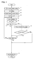
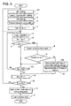
- Fig. 1 is a schematic diagram of laser processing method showing an embodiment of the invention.
- the laser processing apparatus of the invention starts operation and proceeds in the following steps: laser beam output condition setting step 1, desired laser irradiation or process count NsD setting step 2, desired reflection value setting step 3, initializing step 4 of resetting the irradiation or process count Ns to 0, and laser beam irradiation step 5.
- the laser processing apparatus prior to start of laser processing, sets the output condition of laser according to the object to be processed at laser output condition setting step 1. Consequently, the laser irradiation setting step 2 sets the desired laser irradiation or process count NsD. Setting of the irradiation or process count is determined preliminarily depending on the material of the insulating layer, processing precision, and finishing quality target of such object to be processed as a printed circuit board.
- the detection value setting step 3 sets the criterion of a desired detection value of reflected laser beam when the hole position, hole size and hole shape of the conductive layer of the printed circuit board are normal.
- the initializing step 4 resets the laser irradiation or process count Ns to 0.
- the laser processing apparatus processes the printed circuit board. Further, the laser processing apparatus proceeds, through process count up step 6, to process count judging step 7.
- the laser processing apparatus goes to irradiation judging step 10, which judges if the laser irradiation or process count Ns has reached the desired laser irradiation or process count NsD or not.
- the laser processing apparatus goes to the laser irradiation judging step 10, which judges if the laser irradiation or process count Ns has reached the set value or not. If, at the desired detection value judging step 9, the reflected light from the object to be processed is not desired detection value, that is, if the detection value is an abnormal value, the laser processing apparatus goes to laser process stopping step 11, and immediately stops the laser processing. As a result, in the case of such abnormality, the laser processing apparatus immediately stops the laser processing operation, so that the subsequent wasteful process is omitted.
- the laser processing apparatus At the laser irradiation judging step 10, if the laser irradiation or process count Ns has not reached the set value NsD (Ns ⁇ NsD), the laser processing apparatus returns to the laser irradiation step 5, and repeats the subsequent steps.
- the laser processing apparatus goes to the laser process stopping step 11, and immediately stops the laser processing. Thus, processing of one hole is finished.
- the laser processing apparatus or processing method in the embodiment shown in Fig. 1 it process a printed circuit board including at least two layers which are a conductive layer (for example, a copper foil) and an insulating layer (for example, a resin), and which are adjacent to each other and differing in chemical composition from each other .
- the object to be processed is the resin of the insulating layer which is exposed at a plurality of holes opened in the surface layer of the conductive layer and which is irradiated with laser beam.
- the laser processing apparatus Upon irradiating laser beam first, the laser processing apparatus detects the reflected laser beam from the surface of the printed circuit board and stops laser processing immediately if the detection is out of the desired set value.
- the laser processing apparatus inspects the printed circuit board first, then processes, so that it, therefore, can find out a deviation of hole position or abnormality in hole size or hole shape of the copper foil just before processing.
- the laser processing apparatus and processing method in the embodiment shown in Fig.1 by applying laser beam, it processes a printed circuit board having at least two layers which are a conductive layer (for example, a copper foil) and an insulating layer (for example, a resin), and which are adjacent to each other and different in chemical composition from each other.
- the laser processing apparatus Upon detecting the reflected laser beam from the surface of the printed circuit board, when an abnormal value is detected, the laser processing apparatus stops laser processing immediately without starting processing of the insulating layer , and when a normal desired value is detected, the laser processing apparatus starts processing of the insulating layer.
- abnormality of the object to be processed can be detected just before starting process without requiring any extra step for inspection.
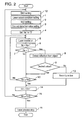
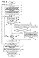
- Fig. 2 is a schematic diagram of laser processing method showing other embodiment of the invention.
- Fig. 2 to avoid duplication of description, only the parts different from those in Fig. 1 are explained herein.
- Substantial difference in Fig. 2 from the embodiment in Fig. 1 is that the information about abnormal hole position is recorded if abnormal value of reflected laser beam is detected.
- the laser processing apparatus of the embodiment first sets the number of holes NhD to be made in the printed circuit board at hole number setting step 12. As the subsequent steps 1 to 11 are same as in Fig. 1, so they are not explained herein.
- the laser processing apparatus goes to hole number count up step 14.
- the hole number judging step 15 judges if the hole number Nh has reached the desired value NhD or not.
- the desired number NhD Nh ⁇ NhD
- the hole number judging step 15 judges if the hole number Nh has reached the desired value NhD or not.
- the process Before reaching the desired number NhD (Nh ⁇ NhD), the process returns to the beginning, that is, the hole number setting step 12, or the laser beam irradiation step 5. Then the process repeats the subsequent steps until the hole number Nh reaches the desired number NhD (Nh ⁇ NhD). Thus, processing of specified number of holes NhD is completed.
- the laser processing apparatus goes to position recording step 13. After the position recording step 13 records the abnormal hole position of the object to be processed , the laser processing apparatus goes to hole number count up step 14, and then goes to process of next hole. In this case, the hole number is counted up whether abnormal value of reflected laser beam is detected or not in the each laser processing. By repeating this operation for the specified number of holes, the laser processing apparatus records the information about positions of all abnormal holes in which detection values are abnormal, and processes all holes of normal detected values. When processing of all normal holes is finished, the laser processing operation is terminated.
- abnormality By detecting the reflected laser beam by the first laser irradiation in laser processing, if there is abnormality in position, diameter or shape of hole of the copper foil, abnormality can be judged without requiring other inspection process. Moreover, as the data of all hole positions of abnormal hole is recorded, so the recorded data can be utilized in re-inspection after process, re-processing and subsequent step, or utilized in fine adjustment or re-setting of conditions at the laser output condition setting step 1.
- either the laser may be applied to one hole continuously or in pulse train, or the laser may be applied hole by hole sequentially to plural holes existing in a certain working area. In either case, the laser processing apparatus obtains the same effects as described above .
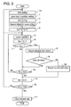
- Fig. 3 is a schematic diagram of laser processing method showing a different embodiment of the invention.
- the laser processing apparatus stops laser processing of the insulating layer corresponding to an abnormal hole in the conductive layer when the detection of reflected laser beam is an abnormal value out of the desired value, and further records the information about the abnormal value of the abnormal hole.
- the laser processing apparatus of the embodiment judges the reflected laser beam from the object to be processed at the desired value detection step 9. If it is out of the desired value, that is, an abnormal value, the process goes to abnormal position and value recording step 16. After recording the position, diameter and shape of abnormal hole of the object to be processed at the abnormal position and value recording step 16, the laser processing apparatus goes to hole number count up step 14, and then starts processing of next hole.
- the laser processing apparatus realizes inspection of abnormality at processing point. Further, since the numerical values of diameter and shape of abnormal hole are recorded, they can be useful in fine adjustment, in re-adjusting of more accurate conditions, in re-inspection, in post-processing, in re-processing, in subsequent step, or in adjusting laser output condition.
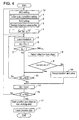
- Fig. 4 is a schematic diagram of laser processing method showing a further different embodiment of the invention.
- Fig.4 to avoid duplication of description, only the parts different from those in Fig. 3 are explained herein.
- the laser processing method of Fig. 4 in addition to the method of Fig. 3, the information about positions of abnormal holes and abnormal values is marked in the non-working area of the circuit board.
- the laser processing apparatus of the embodiment goes to laser marking step 17.
- the laser marking step 17 marks the necessary information among from the position, diameter, and shape of abnormal holes by laser beam as character data or symbol in the non-working area of the printed circuit board , based on the data recorded in the position and value recording step 16.
- the laser processing apparatus After completely marking at the laser marking step 17, the laser processing apparatus goes to laser process stopping step 11 to finish the processing.
- an operator can visually recognize the abnormal hole by the character and symbol marked on multi-layer printed circuit board. Therefore, the operator can easily re-inspect or re-process the multi-layer printed circuit board. It is further advantageous that the operator not only can inspect deviation of hole position or abnormality of hole diameter or hole shape easily, but also can adjust finely and re-enter the accurate conditions, referring to the character and symbol data,.
- Fig. 5 is a schematic diagram of laser processing method showing a further different embodiment of the invention. In Fig.5, to avoid duplication of description, only the parts different from those in Fig. 4 are explained herein.
- the laser processing apparatus judges the reflected laser beam from the object to be processed at the desired value detection step 9. If the reflected laser beam from the object to be processed is out of the desired value, that is, an abnormal value, it goes to position and value storing step 18.
- the position and value storing step 18 stores the information about position and abnormal value in such a secondary storage device as hard disk drive. After storing the values, positions, diameters and shapes of abnormal hole in such secondary storage device as hard disk drive, the laser processing apparatus goes to next recording step 19 a in recording means.
- the recording step 19 converts the information about position, diameter and shape of abnormal holes into data of characters, numerals and symbols, which are easily marked on the surface of the printed circuit board. After the recording step 19, the laser processing apparatus goes to hole number count up step 14, and then starts to process next hole.
- any operator can visually recognize the character, numeral and symbol data marked on multi-layer printed circuit board, and therefore the operator can easily re-inspect or re-process the multi-layer printed circuit board.
- the data stored in the storing means such as hard disk drive can not only be utilized in marking on abnormal positions in the multi-layer printed circuit board, but also can be used in post-process analysis and in quality control in cooperation with computer system.
- the operator of the apparatus can adjust and re-enter the accurate conditions finely, while referring to the character data.
- Fig. 6 is a schematic diagram of laser processing method showing a further different embodiment of the invention.
- Fig. 6 to avoid duplication of description, only the parts different from those in Fig. 5 are explained herein.
- the necessary information about abnormal holes is marked in a non-working area near the corresponding abnormal holes.
- the laser processing apparatus goes to abnormal position marking step 20.
- the abnormal position marking step 20 marks by laser beam at abnormal position of the multi-layer printed circuit board, based on the information stored in the secondary store device such as hard disk drive during storing step 18 as well as based on the data converted and recorded at the recording step 19. Those marks are, for example, circular marks surrounding the processed holes, dots or circles near the processed holes, or some characters. Afterwards, the laser processing apparatus terminates the process at laser process stopping step 11.
- abnormal data and abnormal positions are marked by laser beam, but the same effects are obtained by marking with stamp, ink or other marking means.
- Fig. 7 is a schematic diagram of laser processing method showing a further different embodiment of the invention. In Fig. 7, to avoid duplication of description, only the parts different from those in Fig. 6 are explained herein.
- the detecting step 8 of Fig. 6 is replaced by peak detecting step 21.
- the laser processing apparatus detects the peak value of the reflected laser beam from the multi-layer printed circuit board, and uses this peak value as the detected value. Then the laser processing apparatus goes to desired detection value judging step 9.
- This embodiment is advantageous in that since the peak value of the reflected laser beam is used, the laser processing apparatus can be improved in processing precision, in processing speed, and in processing of quality.
- Fig. 8 is a schematic diagram of laser processing method showing a further different embodiment of the invention.
- Fig. 8 to avoid duplication of description, only the parts different from those in Fig. 7 are explained herein.
- the detected value is obtained from both reflected laser beam and incident laser beam.
- the reflected laser beam peak detecting step 21 of Fig. 7 is replaced by incident and reflected peak detecting step 22 and reflected and incident ratio detecting step 23.
- incident and reflected peak detecting step 22 peak values of incident laser beam to the object to be processed and reflected laser beam therefrom are detected.
- the subsequent process of the laser processing apparatus is same as in Fig. 7.
- This embodiment is advantageous in that since the ratio of incident laser beam peak value and reflected laser beam peak value is used, the processing precision of the laser processing apparatus can be further improved, and in that the processing speed is further accelerated, so as to realize high quality.
- Fig. 9 is a schematic diagram of laser processing method showing a further different embodiment of the invention.
- Fig. 9 to avoid duplication of description, only the parts different from those in Fig. 7 are explained herein.
- the integral value of reflected laser beam is detected, and this integral value is used as the detected value.
- the peak detecting step 21 of Fig. 7 is replaced by integration detecting step 24.
- the integration detecting step 24 detects the integral value of reflected laser beam from the printed circuit board.
- the laser processing apparatus obtains the integral value of reflected laser beam at the integration detecting step 24 as the detected value, which is transmitted it to the next desired detection value judging step 9.
- the subsequent process of the laser processing apparatus is same as in Fig. 7 or Fig. 8.
- This embodiment is advantageous in that since the integral value of the reflected laser beam is used, the laser processing apparatus operates stably.
- Fig. 10 is a schematic diagram of laser processing method showing a further different embodiment of the invention.
- fig.10 to avoid duplication of description, only the parts different from those in Fig. 9 are explained herein.
- the laser processing method of the embodiment of Fig. 10 different from Fig. 9, both the integral value of reflected laser beam and integral value of incident laser beam are detected.
- the value of dividing the integral value of reflected laser beam by the integral value of incident laser beam is used as the detected value.
- reflected laser beam integration detecting step 24 of Fig. 9 is replaced by both incident and reflected integration detecting step 25 and reflected light/incident laser beam ratio detecting step 26.
- the incident laser beam and reflected laser beam integration detecting step 25 detects integral values of incident laser beam to the printed circuit board and reflected laser beam therefrom.
- the laser processing apparatus transmits this detected value to the next desired value judging step 9.
- the subsequent process of the laser processing apparatus in Fig. 10 is same as in Fig. 9.
- This embodiment is further advantageous in that since the ratio of the integral value of the reflected laser beam to the integral value of incident laser beam is used, the laser processing apparatus is further improved in stability.
- Fig. 11 is a schematic diagram of laser processing method showing a further different embodiment of the invention.
- Fig.11 to avoid duplication of description, only the parts different from those in Fig. 10 are explained herein. Other steps are same as in Fig. 10, and are not explained herein.
- the lower limit and upper limit of desired value of detection are determined, and the detected value is judged to be abnormal when the detected value is out of the range between the lower limit and the upper limit.
- desired laser irradiation NsD setting step 2 is followed by upper limit setting step 27 and lower limit setting step 28.
- the setting order of upper limit and lower limit may be reverse.
- the upper limit setting step 27 determines the upper limit of desired detected value to be detected in processing.
- the lower limit setting step 28 determines the lower limit of desired detected value to be detected in.
- the laser processing apparatus goes to desired detection value judging step 29.
- the desired detection value judging step 29 judges if the reflected laser beam from the printed circuit board and incident laser beam thereto are within the range of the desired lower limit and upper limit.
- the laser processing apparatus goes to the irradiation judging step 10.
- the laser processing apparatus goes to the abnormality storing step 18 for storing numerical values of position, diameter, and shape of abnormal hole, and then to the recording step 19.
- This embodiment is advantageous in that since laser processing is operated by judging if the detected value is within the desired lower limit and desired upper limit, the laser processing apparatus is further improved in processing precision , accelerated in processing speed, in high quality processes, and in and stable and smooth operation.
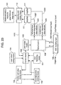
- Fig. 12 shows a supplementary explanation of the laser processing method and apparatus relating to the embodiments of Fig. 1 to Fig. 11, and is an schematic diagram of an embodiment of laser processing apparatus for detecting position deviation of hole and abnormality of hole diameter and hole shape of the printed circuit board.
- Fig. 12 is mostly common to Fig. 1 to Fig. 11, and is explained by summing up.
- a laser generator 30 generates laser beam 31.
- a beam splitter 32 splits the laser beam 31 into two beams. That is, the beam splitter 32 reflects the majority of laser beam 31 to obtain reflected laser beam 321, and allows to pass the rest of the laser beam 31 to obtain transmission laser beam 322.
- the reflected laser beam 321 is sent to the laser processing unit.
- the transmission laser beam 322 is used for correction of fluctuation of laser output.
- a focusing lens 33 focuses the transmission laser beam 322, and sends it to an incident laser beam detector 34.
- the incident laser beam detector 34 detects the transmission laser beam 322, and amplifies by an amplifier 45 to obtain an incident laser beam signal 451 which is sent to a signal processing unit 47.
- a thin film polarizer (TFP) 35 polarizes and separates the reflected laser beam 321. That is, the TFP 35 reflects the reflected laser beam 321 in the direction of 90 degree in the vertical direction, so as to obtain a vertically polarized laser beam 351.
- a quarter wavelength( ⁇ /4) plate 36 converts the vertically polarized laser beam 351 into a circular polarized laser beam 361.
- a focus lens 38 focuses the circular polarized laser beam 361, so as to obtain a focused laser beam 381.
- the focused laser beam 381 is applied to a printed circuit board 37, and a reflected laser beam is obtained and used in processing.
- the focused laser beam 381 is absorbed in an insulating layer 39 exposed at the hole of a copper foil 40 of the printed circuit board 37.
- the copper foil 40 of the printed circuit board 37 reflects the focused laser beam 381, so as to obtain a reflected laser beam 41.
- the laser beam 31 is applied to a normal hole, a specific reflected laser beam 41 from the copper foil surface is detected, but no reflected laser beam 41 is detected in the area of insulating layer 39.
- the hole (area of no copper foil) of the copper foil 40 is made by etching or the like.
- the position of the hole of the copper foil 40 of the surface layer is deviated from the design value or desired value, if the shape of the hole is distorted, or if the hole diameter is smaller, the reflected light 41 is usually larger than a specified value. As a result, abnormality of hole is detected. If the focused laser beam 381 detects this abnormality, then the system stops to make a hole in the insulating layer. If the focused laser beam 381 detects no abnormality, then the system makes a hole in the insulating layer.
- the reflected laser beam 41 reflected on the surface of the copper foil 40 of the board 37 returns to the TFP 35 in the laser beam route.
- the circular polarized vector of focused laser beam 381 is inverted in the direction of polarization when it is reflected on the surface of the copper foil.
- the quarter wavelength ( ⁇ / 4) plate 36 converts the reflected laser beam 41 to a linear polarized laser beam 352 of which plane of polarization is in the horizontal direction. This time, the TFP 35 allows to pass the linear polarized laser beam 352.
- the beam splitter 42 weakens the intensity of the linear polarized laser beam 352.
- the focus lens 43 focuses the weakened linear polarized laser beam 421, so as to obtain a reflected focused laser beam 431.
- a reflected laser beam detector 44 detects the reflected focused laser beam 431.
- the beam splitter 42 may be omitted depending on the intensity of laser beam passing through the TFP 35, or intensity of the reflected focused laser beam 431 to be entered in the reflected laser beam detector 44.
- Amplifier 46 amplifies the reflected and focused laser beam 431, and sends an amplified signal 461 to the signal processing unit 47.
- the signal processing unit 47 processes an incident laser beam signal 451 obtained from the incident laser beam 31 and the reflected and amplified signal 461 obtained from the reflected light 41, so as to generate a normalized signal 471.
- the normalized signal 471 is sent to a hole judging unit 48.
- the hole judging unit 48 compares the normalized signal 471 with a criterion 491 obtained in the detection reference setting unit 49, so as to obtain a judgement signal 481.
- a control device 50 generates a control signal 501 depending on the judgement signal 481, and the control signal 501 controls the laser generator 30, so as to correct the fluctuation of laser output.
- the criterion 491 is determined for the normal hole or abnormal hole preliminarily.
- the hole judging unit 48 judges the hole is normal when the detection signal 471 is within the criterion 491. When the detection signal 471 is out of the criterion 491, it is judged that there is abnormality in position, diameter or shape of the hole.
- the normalized signal 471 is produced as follows.
- the intensity of the reflected laser beam signal 461 is corrected as required.
- the actual correction is as follows.
- the reflected laser beam reflected from the copper foil 40 of the board 37 may not return completely (100%) to the reflected laser beam detector 44.
- the percentage of the reflected laser beam 41 returning from the working position of the printed circuit board 37 is prepared in a coefficient table, and the reflected laser beam signal 461 is corrected according to the coefficient table in the coordinates of each working position.
- the rate of the reflected laser beam returning from the coordinates is 80%, and the reflected laser beam signal detected in the reflected laser beam detector 44 is 8 V, the coefficient of the position is 0.8.
- the signal is amplified by using the amplifier 45 or 46, but the signal sent out from the incident laser beam detector 34 or reflected laser beam detector 44 is sufficiently large, the amplifier 45 or 46 is not always required.
- the laser may generate laser beam in pulse train or continuously depending on the object to be processed.
- a bench for mounting the printed circuit board used in the embodiment may be either a fixed bench or a movable bench moving, for example, in the XY direction of the apparatus. The same results are obtained in both cases.
- the scanning mirror of the optical system may be, for example, galvano-mirror, polygonal mirror, mirror using phono-optical element, a mirror using electro-optical element, or hologram scanner. Same action and effect are obtained by any one of these mirrors.
- the focus lens for processing may be, for example, F ⁇ lens (multi-focus lens), single focus lens, and multiple combination of Fresnel lenses. Same action and effect are obtained by any one of these lenses.
- laser may be emitted continuously to one hole, or laser may be applied to plural holes existing in a certain working area in turn cyclically, which is known as cyclic process.
- cyclic process the same results in action and effect are obtained by either method.
- the type of the laser generation mode or the type of the laser to be used depends on the material of the printed circuit board.
- laser of long wavelength for example, carbon dioxide (CO 2 ) laser of 10.6 ⁇ m is used, or in the case of an ordinary resin circuit board, YAG laser or Excimer laser is used, or their second-order or third-order higher harmonics of laser beam may be used.
- CO 2 carbon dioxide
- an abnormal working position is marked with a circle or the like by laser, but the same effect is obtained by marking a circle by stamp or other printing method. Also the same effect is obtained by marking a hole of an abnormal working position manually.
- the laser processing apparatus of the invention further comprises a video camera, a monitor display showing the image being taken by the video camera, a bench on which a circuit board is mounted as the object to be processed, means for moving the relative positions of the video camera and bench, for example in the X-Y direction, and means for controlling the relative positions corresponding to irradiation of laser beam.
- the video camera takes the image of the working position during laser beam irradiation, and the operator can observe the state of the working position on the screen of the monitor display. It is advantageous that by moving a camera (not shown in the drawings) or bench in relative position regarding to an abnormal hole position and using a suited inspection program, the operator can inspect easily and precisely the abnormal hole position and hole shape.
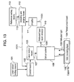
- Fig. 13 is a schematic diagram of laser processing apparatus showing other embodiment of the invention.
- the laser processing apparatus in Fig. 13 emits laser beam and processes the insulating layer corresponding to the holes in the circuit board including at least two layers, that is, the conductive layer having a plurality of holes disposed on the surface layer of the insulating layer to be processed.
- the laser processing apparatus comprises means for irradiating laser beam, means for detecting reflected laser beam, means for stopping laser processing of the insulating layer when the detection of the reflected laser beam is an abnormal value out of the desired value, and means for processing the insulating layer corresponding to the holes when the detection of the reflected laser beam is a desired value.
- Laser output setting means 101 sets the laser output number and the laser output condition, which are the laser processing condition.
- the laser output number is the actual number of working positions or hole number in the printed circuit board.
- the laser output condition shows the laser output energy and working dimensions in individual working positions.
- the laser output setting means 101 sends the processing conditions including the laser output number and laser output condition to control means 102.
- the control means 102 controls a laser output means 103 to emit a laser beam 107 to an optical system 108 based on the processing condition set by the setting means 101.
- the optical system 108 applies the laser beam 107 to the object to be processed, that is, printed circuit board 104.
- the laser beam 107 applied to the printed circuit board first inspects the state of a copper foil 106 near the working position before processing of the insulating layer.
- the copper foil 106 on the surface of the printed circuit board 104 reflects this first laser beam 107, and returns the reflected laser beam 109 to the optical system 108.
- the insulating layer 105 is exposed in the area where the copper foil has been removed by etching beforehand.
- the exposed area of the insulating layer 105 absorbs the laser beam 107.
- the reflected laser beam 109 from the copper foil 106 advances in an optical path reverse to laser irradiation, and reaches the optical system 108.
- the optical system 108 separates the reflected laser beam 109 by its internal separating optical system.
- the separated reflected laser beam component 1091 is guided into a reflected laser beam detector 110.
- the reflected laser beam detector 110 detects the reflected laser beam 109, and transmits a detection signal 1101 to an amplifier 111.
- the amplifier 111 amplifies the detection signal 1101, and transmits to detection judging means 112.
- the detection judging means 112 compares the amplified detection signal 1101 with a specified criterion 1131 preset in reference setting means 113, and judges if the amplified detection signal 1101 is within the specified criterion 1131 or not.
- the detection judging means 112 sends the result 1121 of judgement to the control means 102.
- the control means 102 stops the laser processing if the amplified detection signal 1101 is out of the specified criterion 1131, and on the other hand, continues hole making in the insulating layer 105 of the circuit board 104 when the amplified detection signal 1101 is within the specified criterion 1131.
- the reflected laser beam 109 reflected from the copper foil 104 of the printed circuit board 104 may not return completely (100%) to the reflected laser beam detector 110.
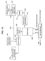
- Fig. 14 is a schematic diagram of laser processing apparatus showing a different embodiment of the invention corresponding to the laser processing method in Fig. 2.
- the embodiment in Fig. 14 is mostly same as the embodiment in Fig. 13, and duplicate explanation is avoided.
- the embodiment in Fig. 14 differs from Fig. 13 in that position recording means 114 for recording the position of an abnormal hole is added. Therefore, the position recording means 114 is mainly explained here.
- the detection judging means 112 sends the result 1121 of judgement to the control means 102.
- the control means 102 records the working position in the position recording means 114, and stops laser processing in the hole.
- the control means 102 continues to make the laser output means 103 emit laser beam so as to process the hole.
- the embodiment is advantageous in that since the position of abnormal hole is kept in the position recording means 114, the recorded data can be useful in re-inspection after processing, re-processing and post-processing. As a result, an overall yield is improved.
- Fig. 15 is a schematic diagram of laser processing apparatus showing a further different embodiment of the invention corresponding to the laser processing method of Fig. 3.
- the laser processing apparatus in the embodiment of Fig. 15 differs from Fig. 14 in that the position recording means 114 in Fig. 14 is replaced by the means for recording the position and abnormal value of abnormal hole, that is, position and value recording means 115.
- the embodiment of Fig. 15 is mostly same as the embodiment of Fig. 14, and in order to avoid duplicate explanation, herein, mainly the position and value recording means 115 is explained.
- the detection judging means 112 sends the result 1121 of judgement to the control means 102.
- the control means 102 records the working position and detected value as the result of detection in the position and value recording means 115, and then stops laser processing in the hole.
- the control means 102 continues to make the laser output means 103 emit laser beam so as to process the hole.
- the embodiment is advantageous in that abnormality in the position, diameter or shape of hole of copper foil can be judged without requiring any extra step for inspection. It is further advantageous that since the position of all abnormal holes and its detected value are recorded, they can be utilized in re-inspection after processing, re-processing and post-processing.
- Fig. 16 is a schematic diagram of laser processing apparatus showing a further different embodiment of the invention corresponding to the laser processing method of Fig. 4.
- the laser processing apparatus in the embodiment of Fig. 16 differs from Fig. 15 in that it further comprises means for recording the position of abnormal hole and/or abnormal value and means for marking the information about position of abnormal hole and/or abnormal value in a non-working area of the circuit board.
- Fig. 16 The embodiment in Fig. 16 is mostly same as the embodiment in Fig. 15, and in order to avoid duplicate explanation, herein, relating to the position and value recording means 115, mainly the recording means 117 and marking means(not shown in the drawings) are explained.
- the detection judging means 112 sends the result 1121 of judgement to the control means 102.
- the control means 102 records the working position and detected value as the result of detection in the position and value recording means 115, and then stops laser processing in the hole.
- the control means 102 continues to make the laser output means 103 emit laser beam so as to process the hole.
- the laser processing apparatus repeats this operation until processing of all holes on the printed circuit board 104 is completed.
- the position and value recording means 115 records all data 1151 including position, diameter and shape of all abnormal holes.
- the position and detected value recording means 115 sends the data 1151 to the recording means 117.
- the recording means 117 compiles marking data 1171 based on the data 1151, and sends to the control means 102.
- the control means 102 controls the laser output means 103 and optical system 108 based on the marking data 1171, so as to mark the marking data 1171 as character data or symbol in the non-working area of the printed circuit board.
- the embodiment is advantageous in that the operator can utilize the data 1151 recorded in the position and detected value recording means 115 in re-inspection after processing, re-processing and post-processing. It is advantageous that the operator can visually recognize the marking data 1171 marked in characters on the surface of the printed circuit board, and hence can re-inspect or re-process smoothly according to the marking data 1171.
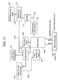
- Fig. 17 is a schematic diagram of laser processing apparatus showing a further different embodiment of the invention corresponding to the laser processing method of Fig. 5.
- the laser processing apparatus differs from Fig. 16 in that it further comprises means for storing at least one of the position of abnormal hole and abnormal value in such secondary storage means as hard disk drive, that is, position and detected value storing means 118.
- Fig. 17 is same as the embodiment of Fig. 16 in other parts, and in order to avoid duplicate explanation, herein, only the parts relating to the position and detected value storing means 118 are explained.
- the detection judging means 112 sends the result 1121 of judgement to the control means 102.
- the control means 102 stores the data 1181 such as working position and detected value as the result of detection in the position and value storing means 118, and then stops laser processing in the hole.
- the control means 102 continues to make the laser output means 103 emit laser beam so as to process the hole.
- the recording means 117 compiles marking data 1171 based on the data 1181 stored in the position and value storing means 118, and then sends the marking data to the control means 102.
- the other operation is same as in Fig. 16.
- the embodiment is advantageous in that the operator can utilize the data 1181 stored in the position and value storing means 118 in re-inspection after processing, re-processing and post-processing. For example, the operator can visually recognize the marking data 1171 marked in characters on the surface of the printed circuit board, and hence can re-inspect or re-process more smoothly. It is further advantageous that since the data 1181 stored in the position and detected value storing means 118 such as hard disk drive can be taken into other computer or the like and the information can be processed, so that the data 1181 can be utilized in process control or quality control.
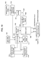
- Fig. 18 is a schematic diagram of laser processing apparatus showing a further different embodiment of the invention corresponding to the laser processing method of Fig. 6.
- the laser processing apparatus in Fig. 18 differs from Fig. 17 in that it further comprises means for marking the information about abnormal hole in non-working area near the corresponding abnormal hole, that is, abnormal position marking means 119.
- Fig. 18 is same as the embodiment in Fig. 17 in other parts, and in order to avoid duplicate explanation, herein, only the parts different from Fig. 17, that is, the added abnormal position marking means 119, is mainly explained.
- the abnormal position marking means 119 converts the data 1182 stored in the position and detected value storing means 118 such as hard disk drive into marking data.
- abnormal position data 1182 is converted into marking data 1191 such as circle, character, numeral or other symbol to be marked around the hole.
- marking data 1191 such as circle, character, numeral or other symbol to be marked around the hole.
- information about abnormal value may be marked.
- the control means 102 controls the laser output means 103 and optical system 108 in turn, so as then to mark circle, character, numeral or other symbol on the surface of free space near the abnormal part of the printed circuit board 104.
- the operator can see the mark and recognizes abnormality in processing, and also can refer to the data 1181 of the position and detected value storing means 118, and that he can make re-inspect the printed circuit board 104 quickly, and also can inspect or correct and process the printed circuit board 104 adequately. As a result, the yield of the printed circuit board can be further improved.
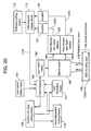
- Fig. 19 is a schematic diagram of laser processing apparatus showing a further different embodiment of the invention corresponding to the laser processing method in Fig. 7.
- the laser processing apparatus differs from Fig. 18 in that the reflected light detecting means 110 in Fig. 18 is replaced by means 120 for detecting the peak value of reflected light, and that this peak value is used as the detected value.
- Fig. 19 is same as the embodiment in Fig. 18 in other parts, and in order to avoid duplicate explanation, herein, only the part different from Fig. 18, that is, the reflected light peak detecting means 120 is mainly explained.
- the reflected laser beam 109 from the copper foil 106 of the printed circuit board 104 advances in the optical path reverse to laser irradiation, and then reaches the optical system 108.
- the optical system 108 separates the reflected laser beam 109 by its internal separating optical system.
- the separated reflected component 1091 is guided into the peak detector 120.
- the peak detector 120 detects the peak value 1201 of the reflected component 1091, and then transmits a peak value 1201 to the amplifier 111.
- the embodiment is advantageous in that since the laser processing apparatus makes use of the peak value 1201 of reflected laser beam in the inspection mode, then the speed and precision of inspection are improved.
- Fig. 20 is a schematic diagram of laser processing apparatus showing a further different embodiment of the invention corresponding to the laser processing method of Fig. 8.
- the laser processing apparatus of Fig. 20 differs from Fig. 19 in that it further comprises means 120 and 121 for detecting the peak of reflected laser beam and peak of incident laser beam, and in that the value of the peak of reflected laser beam divided by the peak of incident laser beam is used as the detected value.
- the embodiment in Fig. 20 is same as the embodiment in Fig. 19 in other parts, and in order to avoid duplicate explanation, herein, only the part different from Fig. 19, that is, the incident laser beam peak detecting means 121 is mainly explained.
- the reflected laser beam 109 from the copper foil 106 of the printed circuit board 104 advances in the optical path reverse to laser irradiation, and reaches the optical system 108.
- the optical system 108 separates the reflected laser beam 109 by its internal separating optical system.
- the separated component 1091 is guided into the peak detector 120.
- the peak detector 120 detects the peak value 1201 of the reflected component 1091, and then transmits a peak value 1201 to the amplifier 111.
- the laser processing apparatus guides a part 1081 of incident laser beam from the laser branched in the optical system 108 into the incident peak detector 121.
- the incident peak detector 121 detects the incident laser beam peak value 1211, and transmits it to the amplifier 111.
- the amplifier 111 amplifies the signal, and then transmits it to detection judging means 112.
- the reference setting means 113 sends the result 1121 of judgement to the control means 102.
- the embodiment is advantageous in that as the laser processing apparatus makes use of the ratio of the reflected peak value 1201 and incident peak value 1211 in the inspection mode, then the operation is stable regardless of fluctuations of the output of laser beam, and further in that the speed and precision of inspection are improved.
- Fig. 21 is a schematic diagram of laser processing apparatus showing a further different embodiment of the invention corresponding to the laser processing method of Fig. 9.
- the laser processing apparatus of Fig. 21 differs from Fig. 19 or Fig. 20 in that it further comprises means 122 for detecting the integral value of reflected light, and in that the integral value is used as the detected value.
- Fig. 21 is same as the embodiment of Fig. 19 or Fig. 20 in other parts
- the reflected laser beam integral value detecting means 122 is mainly explained.
- the reflected laser beam 109 from the copper foil 106 of the printed circuit board 104 advances in the optical path reverse to laser irradiation, and then reaches the optical system 108.
- the optical system 108 separates the reflected laser beam 109 by its internal separating optical system.
- the separated reflected component 1091 is guided into the reflected laser beam integral value detecting means 122.
- the reflected integral value detecting means 122 integrates the reflected component 1091 in order to eliminate fluctuations of laser output by noise component, and transmits the reflected integral detected value 1211 to the amplifier 111.
- the subsequent operation of the laser processing apparatus is same as in the foregoing embodiment, and is not explained herein.
- the embodiment is advantageous in that as the laser processing apparatus makes use of the reflected integral value 1221 in inspection mode, therefore the operation is stable regardless of fluctuations of the output of laser beam due to noise component.
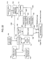
- Fig. 22 is a schematic diagram of laser processing apparatus showing a further different embodiment of the invention corresponding to the laser processing method of Fig. 10.
- the laser processing apparatus of Fig. 22 differs from Fig. 20 or Fig. 21 in that it further comprises means 122 and 123 for detecting the integral value of reflected laser beam and integral value of incident laser beam, and in that the value of dividing the integral value of reflected laser beam by the integral value of incident laser beam is used as the detected value.
- Fig. 22 is same as the embodiment of Fig. 21 in other parts. In order to avoid duplicate explanation, herein, only the part different from Fig. 21, that is, the incident laser beam integral value detecting means 123 is mainly explained.
- the reflected laser beam 109 from the copper foil 106 of the printed circuit board 104 advances in the optical path reverse to laser irradiation, and then reaches the optical system 108.
- the optical system 108 separates the reflected laser beam 109 by its internal separating optical system.
- the separated reflected component 1091 is guided into the reflected integral value detecting means 122.
- the reflected integral value detecting means 122 detects the integral value 1221 of the reflected component 1091, and then transmits the integral value 1221 of the reflected laser beam to the amplifier 111.
- the laser processing apparatus guides the part 1081 of incident laser beam from the laser branched in the optical system 108 into the incident integral value detector 123.
- the incident integral value detector 123 detects the integral value 1231 of incident laser beam, and then transmits it to the amplifier 111.
- the amplifier 111 amplifies the signal, and then transmits it to detection judging means 112.
- the reference setting means 113 sends the result 1121 of judgement to the control means 102.
- the embodiment is advantageous in that as the laser processing apparatus makes use of the ratio of the reflected integral value 1221 and incident integral value 1231 in the inspection mode, therefore the operation is stable regardless of fluctuations of the output of laser beam due to noise component, and further in that the speed and precision of inspection are improved.
- Fig. 23 is a schematic diagram of laser processing apparatus showing a further different embodiment of the invention corresponding to the laser processing method of Fig. 11.
- the laser processing method of Fig. 23 differs from Fig. 22 in that it further comprises means 124 for determining the lower limit and upper limit of desired value, and in that it judges abnormal when the detected value is out of the range of the lower limit and upper limit.
- the laser processing apparatus first sets in the inspection reference setting means 124. Different from the case of Fig. 22, it sets the upper limit and lower limit of the desired criterion.
- the detection judging means 112 judges if the detected value is within the lower limit and upper limit of the desired reference, and then sends the result of judgement to the control means 102.
- the subsequent operation of the laser processing apparatus is same as in the foregoing embodiment, and is not explained herein.
- the embodiment is advantageous in that as the laser processing apparatus makes use of the ratio of the reflected integral value 1221 and incident integral value 1231 in inspection mode , therefore, the operation is stable regardless of fluctuations of the output of laser beam due to noise component, and further the speed and precision of inspection are improved.
- the judging range of the detection judging means 112 is limited, and so the detection judging means 112 can produce the result of judgement quickly.
- the laser processing method or apparatus of the invention since the reflected laser beam of the laser irradiation on the printed circuit board is detected first, abnormality in position, diameter or shape of the hole can be detected just before hole making process. Therefore, it is advantageous, in the laser processing method or apparatus of the invention, that the printed circuit board can be processed without requiring any extra process for prior inspection. It is also advantageous, in the invention, that since the data about abnormal hole is recorded and stored even after laser processing, the operator can easily and smoothly recognize abnormal position and abnormal mode at the time of re-inspection or re-processing. It is further advantageous that in correction at post-processing, the operator can save labor in interlayer connection by solder or conductive paste, and in final product inspection. As a result, it is advantageous that the cycle time of manufacture of printed circuit board is improved, and occurrence of wasteful cost or material loss can be minimized.
Abstract
Description
- The present invention relates to laser processing of printed circuit board, and more particularly to a laser processing method and a laser processing apparatus suitable for forming holes in a multi-layer printed circuit board having an insulating layer and a conductive layer laminated in multiple layers.
- Generally, a multi-layer circuit board is formed by laminating an insulating layer and a conductive layer alternately. Most electronic circuits have come to use widely such multi-layer printed circuit boards which are effective for increasing the mounting density of circuit parts.
- Specifically, holes are formed in an insulating layer of a multi-layer printed circuit board, and the holes are filled with solder or conductive paste, which connect adjacent conductive layers in the multi-layer printed circuit board.
- Thus, the conventional laser processing apparatus makes holes in the insulating layer by employing the laser beam processing technology.
- In the laser processing apparatus, laser beams of long wavelength are often used. This is because laser beams of long wavelength are suitable to be absorbed in the insulating layer and easily reflected on the conductive layer. For example, when the insulating layer to work is a glass epoxy resin with glass fibers in it, and the conductive layer is a copper foil, the processing apparatus processes to remove the insulating layer only selectively by using carbon dioxide(CO2) laser beam.
- When the laser beam opens holes in the resin part exposed in the holes of the copper foil of the printed circuit board, the holes of the copper foil of the surface layer are often deviated from the standard positions of holes or the holes of the copper foil are sometime abnormal in shape and size.
- The conventional laser processing apparatus has continued to process the printed circuit board up to the final step, even if there were position deviation of copper foil holes, abnormal hole diameter and hole shape. In such case, such printed circuit board having small electronic parts mounted on it were not matched in the dimensions, so that such printed circuit board did not operate normally and then it was scrapped as a defective piece. In the conventional laser processing apparatus, products were checked in the final stage, and defective pieces were sorted out the final stage. In another case, the conventional laser processing apparatus utilizes an image recognition process or the like, so as to check the hole position, hole diameter and hole shape of the copper foil of the surface layer , before making hole in the resin part by laser.
- Such prior art had the following problems. In the conventional laser processing apparatus, since the printed circuit boards were checked in the final stage, printed circuit boards must be processed completely up to the final stage, even if they have such defects as abnormality in hole position, hole diameter or hole shape of the copper foil and then they are not usable. As a result, wasteful process, time, material and energy were spent, and the total manufacturing cost was raised in the conventional process.
- In the case of addition of a conventional process for checking the hole position, size and shape by image recognition device before making holes in the resin part by laser processing, such a prior step must be added, and the manufacturing time and cost were increased by this step.
- It is hence an object of the invention to present a method or apparatus for solving these conventional problems. The invention presents a method and an apparatus for making holes in the resin layer while inspecting the hole position, hole diameter and hole shape of the copper foil of the surface layer, hole by hole, using the laser beam, instead of merely making holes in the resin layer of printed circuit board.
- To solve the problems, the invention presents a laser processing method or apparatus for processing a circuit board including at least two layers, having a conductive layer with a plurality of holes disposed on a surface layer of insulating layer to be processed by applying laser beam to an insulating layer corresponding to holes of the conductive layer. In this laser processing method or apparatus, a circuit board is irradiated with a laser beam, and a reflected laser beam is detected, whereby the laser process of the insulating layer corresponding to an abnormal hole in the conductive layer is stopped, if the detected value of the reflected laser beam is an abnormal value out of a desired value. Also in this laser processing method or apparatus, the insulating layer corresponding to the hole is processed when the detected value of the reflected laser beam conforms to the desired value.
-
- Fig. 1 is a schematic diagram of laser processing method showing an embodiment of the invention.
- Fig. 2 is a schematic diagram of laser processing method showing other embodiment of the invention.
- Fig. 3 is a schematic diagram of laser processing method showing a different embodiment of the invention.
- Fig. 4 is a schematic diagram of laser processing method showing a further different embodiment of the invention.
- Fig. 5 is a schematic diagram of laser processing method showing a further different embodiment of the invention.
- Fig. 6 is a schematic diagram of laser processing method showing a further different embodiment of the invention.
- Fig. 7 is a schematic diagram of laser processing method showing a further different embodiment of the invention.
- Fig. 8 is a schematic diagram of laser processing method showing a further different embodiment of the invention.
- Fig. 9 is a schematic diagram of laser processing method showing a further different embodiment of the invention.
- Fig. 10 is a schematic diagram of laser processing method showing a further different embodiment of the invention.
- Fig. 11 is a schematic diagram of laser processing method showing a further different embodiment of the invention.
- Fig. 12 is a schematic diagram of an embodiment of laser processing apparatus for detecting position deviation of holes of the copper foil of printed circuit board, and abnormality of hole diameter or hole shape, as a laser processing apparatus relating to embodiments in Fig. 1 to Fig. 11 of the invention.
- Fig. 13 is a schematic diagram of laser processing apparatus showing other embodiment of the invention.
- Fig. 14 is a schematic diagram of laser processing apparatus showing a different embodiment of the invention.
- Fig. 15 is a schematic diagram of laser processing apparatus showing a further different embodiment of the invention.
- Fig. 16 is a schematic diagram of laser processing apparatus showing a further different embodiment of the invention.
- Fig. 17 is a schematic diagram of laser processing apparatus showing a further different embodiment of the invention.
- Fig. 18 is a schematic diagram of laser processing apparatus showing a further different embodiment of the invention.
- Fig. 19 is a schematic diagram of laser processing apparatus showing a further different embodiment of the invention.
- Fig. 20 is a schematic diagram of laser processing apparatus showing a further different embodiment of the invention.
- Fig. 21 is a schematic diagram of laser processing apparatus showing a further different embodiment of the invention.
- Fig. 22 is a schematic diagram of laser processing apparatus showing a further different embodiment of the invention.
- Fig. 23 is a schematic diagram of laser processing apparatus showing a further different embodiment of the invention.
-
- Fig. 1 is a schematic diagram of laser processing method showing an embodiment of the invention.
- The laser processing apparatus of the invention starts operation and proceeds in the following steps: laser beam output
condition setting step 1, desired laser irradiation or process countNsD setting step 2, desired reflectionvalue setting step 3, initializingstep 4 of resetting the irradiation or process count Ns to 0, and laserbeam irradiation step 5. - The laser processing apparatus, prior to start of laser processing, sets the output condition of laser according to the object to be processed at laser output
condition setting step 1. Consequently, the laserirradiation setting step 2 sets the desired laser irradiation or process count NsD. Setting of the irradiation or process count is determined preliminarily depending on the material of the insulating layer, processing precision, and finishing quality target of such object to be processed as a printed circuit board. The detectionvalue setting step 3 sets the criterion of a desired detection value of reflected laser beam when the hole position, hole size and hole shape of the conductive layer of the printed circuit board are normal. The initializingstep 4 resets the laser irradiation or process count Ns to 0. - At
laser processing step 5, the laser processing apparatus processes the printed circuit board. Further, the laser processing apparatus proceeds, through process count upstep 6, to processcount judging step 7. The process count upstep 6 counts up the process count Ns by one, i.e. Ns = Ns + 1, every time the laser processing apparatus irradiates laser beam to one hole. Next, the process count judgingstep 7 judges if the laser irradiation is the first time or not. In the case of the first irradiation, that is, when the process count Ns is 1 (Ns = 1), the laser processing apparatus detects the reflected laser beam from the object to be processed atreflection detecting step 8, and goes to desired detectionvalue judging step 9. - On the other hand, when the laser irradiation or process count Ns is not first time (Ns > 1), the laser processing apparatus goes to
irradiation judging step 10, which judges if the laser irradiation or process count Ns has reached the desired laser irradiation or process count NsD or not. - Consequently, at the desired detection
value judging step 9, when the reflected laser beam from the object to be processed is within a desired detection value, the laser processing apparatus goes to the laserirradiation judging step 10, which judges if the laser irradiation or process count Ns has reached the set value or not. If, at the desired detectionvalue judging step 9, the reflected light from the object to be processed is not desired detection value, that is, if the detection value is an abnormal value, the laser processing apparatus goes to laserprocess stopping step 11, and immediately stops the laser processing. As a result, in the case of such abnormality, the laser processing apparatus immediately stops the laser processing operation, so that the subsequent wasteful process is omitted. - At the laser
irradiation judging step 10, if the laser irradiation or process count Ns has not reached the set value NsD (Ns < NsD), the laser processing apparatus returns to thelaser irradiation step 5, and repeats the subsequent steps. When the laser irradiation or process count Ns has reached the desired set value NsD (Ns ≧ NsD) at laserirradiation judging step 10, the laser processing apparatus goes to the laserprocess stopping step 11, and immediately stops the laser processing. Thus, processing of one hole is finished. - According to the laser processing apparatus or processing method in the embodiment shown in Fig. 1, it process a printed circuit board including at least two layers which are a conductive layer (for example, a copper foil) and an insulating layer (for example, a resin), and which are adjacent to each other and differing in chemical composition from each other .The object to be processed is the resin of the insulating layer which is exposed at a plurality of holes opened in the surface layer of the conductive layer and which is irradiated with laser beam. Upon irradiating laser beam first, the laser processing apparatus detects the reflected laser beam from the surface of the printed circuit board and stops laser processing immediately if the detection is out of the desired set value. Thus, the laser processing apparatus inspects the printed circuit board first, then processes, so that it, therefore, can find out a deviation of hole position or abnormality in hole size or hole shape of the copper foil just before processing. In other words according to the laser processing apparatus and processing method in the embodiment shown in Fig.1, by applying laser beam, it processes a printed circuit board having at least two layers which are a conductive layer (for example, a copper foil) and an insulating layer (for example, a resin), and which are adjacent to each other and different in chemical composition from each other. Upon detecting the reflected laser beam from the surface of the printed circuit board, when an abnormal value is detected, the laser processing apparatus stops laser processing immediately without starting processing of the insulating layer , and when a normal desired value is detected, the laser processing apparatus starts processing of the insulating layer.
- Thus, by processing while inspecting, abnormality of the object to be processed can be detected just before starting process without requiring any extra step for inspection.
- Fig. 2 is a schematic diagram of laser processing method showing other embodiment of the invention. In Fig. 2, to avoid duplication of description, only the parts different from those in Fig. 1 are explained herein. Substantial difference in Fig. 2 from the embodiment in Fig. 1 is that the information about abnormal hole position is recorded if abnormal value of reflected laser beam is detected.
- In Fig. 2, upon start, the laser processing apparatus of the embodiment first sets the number of holes NhD to be made in the printed circuit board at hole
number setting step 12. As thesubsequent steps 1 to 11 are same as in Fig. 1, so they are not explained herein. - At laser
irradiation judging step 10, when the laser irradiation or process count Ns has reached the desired set value NsD (Ns ≧ NsD), the laser processing apparatus goes to hole number count upstep 14. The hole number count upstep 14 counts up the hole number Nh by adding 1 to Nh (Nh = Nh + 1), and the process goes to holenumber judging step 15. The holenumber judging step 15 judges if the hole number Nh has reached the desired value NhD or not. Upon reaching the desired number NhD (Nh ≧ NhD), it goes to laserprocess stop step 11, so that the laser processing is finished. On the other hand, the holenumber judging step 15 judges if the hole number Nh has reached the desired value NhD or not. Before reaching the desired number NhD (Nh < NhD), the process returns to the beginning, that is, the holenumber setting step 12, or the laserbeam irradiation step 5. Then the process repeats the subsequent steps until the hole number Nh reaches the desired number NhD (Nh ≧ NhD). Thus, processing of specified number of holes NhD is completed. - At desired detection
value judging step 9 of Fig.2 , if the reflected laser beam from the object to be processed is not within a desired value, that is, if the value of the reflected laser beam is abnormal, the laser processing apparatus goes to position recordingstep 13. After theposition recording step 13 records the abnormal hole position of the object to be processed , the laser processing apparatus goes to hole number count upstep 14, and then goes to process of next hole. In this case, the hole number is counted up whether abnormal value of reflected laser beam is detected or not in the each laser processing. By repeating this operation for the specified number of holes, the laser processing apparatus records the information about positions of all abnormal holes in which detection values are abnormal, and processes all holes of normal detected values. When processing of all normal holes is finished, the laser processing operation is terminated. - By detecting the reflected laser beam by the first laser irradiation in laser processing, if there is abnormality in position, diameter or shape of hole of the copper foil, abnormality can be judged without requiring other inspection process. Moreover, as the data of all hole positions of abnormal hole is recorded, so the recorded data can be utilized in re-inspection after process, re-processing and subsequent step, or utilized in fine adjustment or re-setting of conditions at the laser output
condition setting step 1. - Moreover, since laser processing is done while inspecting, abnormality of the object to be processed can be detected just before processing without requiring any extra step for inspection.
- In all embodiments of laser processing shown in Fig. 2 and in the following drawings, either the laser may be applied to one hole continuously or in pulse train, or the laser may be applied hole by hole sequentially to plural holes existing in a certain working area. In either case, the laser processing apparatus obtains the same effects as described above .
- Fig. 3 is a schematic diagram of laser processing method showing a different embodiment of the invention. In Fig. 3, to avoid duplication of description, only the parts different from those in Fig. 2 are explained herein. In the embodiment of Fig.3, in addition to the embodiment of Fig.2, the laser processing apparatus stops laser processing of the insulating layer corresponding to an abnormal hole in the conductive layer when the detection of reflected laser beam is an abnormal value out of the desired value, and further records the information about the abnormal value of the abnormal hole.
- In Fig. 3, the laser processing apparatus of the embodiment judges the reflected laser beam from the object to be processed at the desired
value detection step 9. If it is out of the desired value, that is, an abnormal value, the process goes to abnormal position andvalue recording step 16. After recording the position, diameter and shape of abnormal hole of the object to be processed at the abnormal position andvalue recording step 16, the laser processing apparatus goes to hole number count upstep 14, and then starts processing of next hole. - In this case, in addition to the effect of the embodiment of Fig. 2, aside from recording of all abnormal hole positions out of the desired detection value, the laser processing apparatus realizes inspection of abnormality at processing point. Further, since the numerical values of diameter and shape of abnormal hole are recorded, they can be useful in fine adjustment, in re-adjusting of more accurate conditions, in re-inspection, in post-processing, in re-processing, in subsequent step, or in adjusting laser output condition.
- Fig. 4 is a schematic diagram of laser processing method showing a further different embodiment of the invention. In Fig.4, to avoid duplication of description, only the parts different from those in Fig. 3 are explained herein. In the laser processing method of Fig. 4, in addition to the method of Fig. 3, the information about positions of abnormal holes and abnormal values is marked in the non-working area of the circuit board.
- In Fig. 4, at hole
number judging step 15, when the hole number Nh has reached the desired value NhD (Nh ≧ NhD), the laser processing apparatus of the embodiment goes tolaser marking step 17. Thelaser marking step 17 marks the necessary information among from the position, diameter, and shape of abnormal holes by laser beam as character data or symbol in the non-working area of the printed circuit board , based on the data recorded in the position andvalue recording step 16. - After completely marking at the
laser marking step 17, the laser processing apparatus goes to laserprocess stopping step 11 to finish the processing. - Thus, according to the embodiment of Fig. 4, in addition to the benefits explained in embodiments in Fig. 1 to Fig. 3, an operator can visually recognize the abnormal hole by the character and symbol marked on multi-layer printed circuit board. Therefore, the operator can easily re-inspect or re-process the multi-layer printed circuit board. It is further advantageous that the operator not only can inspect deviation of hole position or abnormality of hole diameter or hole shape easily, but also can adjust finely and re-enter the accurate conditions, referring to the character and symbol data,.
- Fig. 5 is a schematic diagram of laser processing method showing a further different embodiment of the invention. In Fig.5, to avoid duplication of description, only the parts different from those in Fig. 4 are explained herein.
- In Fig. 5, the laser processing apparatus judges the reflected laser beam from the object to be processed at the desired
value detection step 9. If the reflected laser beam from the object to be processed is out of the desired value, that is, an abnormal value, it goes to position andvalue storing step 18. The position andvalue storing step 18 stores the information about position and abnormal value in such a secondary storage device as hard disk drive. After storing the values, positions, diameters and shapes of abnormal hole in such secondary storage device as hard disk drive, the laser processing apparatus goes to next recording step 19 a in recording means. Therecording step 19 converts the information about position, diameter and shape of abnormal holes into data of characters, numerals and symbols, which are easily marked on the surface of the printed circuit board. After therecording step 19, the laser processing apparatus goes to hole number count upstep 14, and then starts to process next hole. - In this case, same as in Fig. 4, in addition to the benefits explained in embodiments in Fig. 1 to Fig. 4, any operator can visually recognize the character, numeral and symbol data marked on multi-layer printed circuit board, and therefore the operator can easily re-inspect or re-process the multi-layer printed circuit board. It is also advantageous that the data stored in the storing means such as hard disk drive can not only be utilized in marking on abnormal positions in the multi-layer printed circuit board, but also can be used in post-process analysis and in quality control in cooperation with computer system. It is further advantageous that at
condition setting step 1 of the laser processing apparatus, the operator of the apparatus can adjust and re-enter the accurate conditions finely, while referring to the character data. - Fig. 6 is a schematic diagram of laser processing method showing a further different embodiment of the invention. In Fig. 6, to avoid duplication of description, only the parts different from those in Fig. 5 are explained herein. In the embodiment of Fig. 6, in addition to the effect of Fig. 5, the necessary information about abnormal holes is marked in a non-working area near the corresponding abnormal holes.
- In Fig. 6, after marking data in character, numeral and symbol on non-working area of circuit board at
laser marking step 17, the laser processing apparatus goes to abnormalposition marking step 20. The abnormalposition marking step 20 marks by laser beam at abnormal position of the multi-layer printed circuit board, based on the information stored in the secondary store device such as hard disk drive during storingstep 18 as well as based on the data converted and recorded at therecording step 19. Those marks are, for example, circular marks surrounding the processed holes, dots or circles near the processed holes, or some characters. Afterwards, the laser processing apparatus terminates the process at laserprocess stopping step 11. - Thus, according to the embodiment shown in Fig. 6, in addition to marking of data by characters in embodiment of Fig. 4 or Fig. 5, it is advantageous that since positions of abnormal processed holes are indicated by marks, the operator can re-inspect or re-process smoothly without any mistake, while observing abnormal positions.
- In the foregoing embodiments, abnormal data and abnormal positions are marked by laser beam, but the same effects are obtained by marking with stamp, ink or other marking means.
- Fig. 7 is a schematic diagram of laser processing method showing a further different embodiment of the invention. In Fig. 7, to avoid duplication of description, only the parts different from those in Fig. 6 are explained herein.
- In the laser processing apparatus of Fig. 7, the detecting
step 8 of Fig. 6 is replaced bypeak detecting step 21. - At
peak detecting step 21, the laser processing apparatus detects the peak value of the reflected laser beam from the multi-layer printed circuit board, and uses this peak value as the detected value. Then the laser processing apparatus goes to desired detectionvalue judging step 9. This embodiment is advantageous in that since the peak value of the reflected laser beam is used, the laser processing apparatus can be improved in processing precision, in processing speed, and in processing of quality. - Fig. 8 is a schematic diagram of laser processing method showing a further different embodiment of the invention. In Fig. 8, to avoid duplication of description, only the parts different from those in Fig. 7 are explained herein. In the embodiment of Fig. 8, in contrast to the peak value, the detected value is obtained from both reflected laser beam and incident laser beam.
- In the laser processing apparatus of Fig. 8, the reflected laser beam
peak detecting step 21 of Fig. 7 is replaced by incident and reflectedpeak detecting step 22 and reflected and incidentratio detecting step 23. At incident and reflectedpeak detecting step 22, peak values of incident laser beam to the object to be processed and reflected laser beam therefrom are detected. At reflected and incidentratio detecting step 23, the ratio of reflected laser beam peak value to incident laser beam peak value is obtained as detected value (detected value = reflected peak value/incident peak value), which are transmitted to the next desired detectionvalue judging step 9. The subsequent process of the laser processing apparatus is same as in Fig. 7. - This embodiment is advantageous in that since the ratio of incident laser beam peak value and reflected laser beam peak value is used, the processing precision of the laser processing apparatus can be further improved, and in that the processing speed is further accelerated, so as to realize high quality.
- Fig. 9 is a schematic diagram of laser processing method showing a further different embodiment of the invention. In Fig. 9, to avoid duplication of description, only the parts different from those in Fig. 7 are explained herein. In the laser processing method of the embodiment in Fig. 9, different from Fig. 7, the integral value of reflected laser beam is detected, and this integral value is used as the detected value.
- In the laser processing apparatus of Fig. 9, the
peak detecting step 21 of Fig. 7 is replaced byintegration detecting step 24. Theintegration detecting step 24 detects the integral value of reflected laser beam from the printed circuit board. The laser processing apparatus obtains the integral value of reflected laser beam at theintegration detecting step 24 as the detected value, which is transmitted it to the next desired detectionvalue judging step 9. The subsequent process of the laser processing apparatus is same as in Fig. 7 or Fig. 8. - This embodiment is advantageous in that since the integral value of the reflected laser beam is used, the laser processing apparatus operates stably.
- Fig. 10 is a schematic diagram of laser processing method showing a further different embodiment of the invention. In fig.10, to avoid duplication of description, only the parts different from those in Fig. 9 are explained herein. In the laser processing method of the embodiment of Fig. 10, different from Fig. 9, both the integral value of reflected laser beam and integral value of incident laser beam are detected. The value of dividing the integral value of reflected laser beam by the integral value of incident laser beam is used as the detected value.
- In the laser processing apparatus of Fig. 10, reflected laser beam
integration detecting step 24 of Fig. 9 is replaced by both incident and reflectedintegration detecting step 25 and reflected light/incident laser beamratio detecting step 26. The incident laser beam and reflected laser beamintegration detecting step 25 detects integral values of incident laser beam to the printed circuit board and reflected laser beam therefrom. The reflected light/incidentratio detecting step 26 calculates and normalizes the ratio of the integral value of reflected laser beam to the integral value of incident laser beam, and then obtains a detected value (detected value = integral value of reflected light/integral value of incident light), so as to eliminate a influence caused by fluctuations of laser output. The laser processing apparatus transmits this detected value to the next desiredvalue judging step 9. The subsequent process of the laser processing apparatus in Fig. 10 is same as in Fig. 9. - This embodiment is further advantageous in that since the ratio of the integral value of the reflected laser beam to the integral value of incident laser beam is used, the laser processing apparatus is further improved in stability.
- Fig. 11 is a schematic diagram of laser processing method showing a further different embodiment of the invention. In Fig.11, to avoid duplication of description, only the parts different from those in Fig. 10 are explained herein. Other steps are same as in Fig. 10, and are not explained herein. In the laser processing method in the embodiment of Fig. 11, different from Fig. 10, the lower limit and upper limit of desired value of detection are determined, and the detected value is judged to be abnormal when the detected value is out of the range between the lower limit and the upper limit.
- In the laser processing apparatus of the embodiment, desired laser irradiation
NsD setting step 2 is followed by upperlimit setting step 27 and lowerlimit setting step 28. The setting order of upper limit and lower limit may be reverse. The upperlimit setting step 27 determines the upper limit of desired detected value to be detected in processing. The lowerlimit setting step 28 determines the lower limit of desired detected value to be detected in. - On the other hand, after the reflected /incident
ratio detecting step 26, the laser processing apparatus goes to desired detectionvalue judging step 29. The desired detectionvalue judging step 29 judges if the reflected laser beam from the printed circuit board and incident laser beam thereto are within the range of the desired lower limit and upper limit. When the detected value is within the range of the desired lower limit and upper limit ,i.e. lower limit ≦ detected value ≦ upper limit, the laser processing apparatus goes to theirradiation judging step 10. When the detected values are not within the range of the desired lower limit and upper limit ,i.e. lower limit > detected value, or detected value > upper limit, the laser processing apparatus goes to theabnormality storing step 18 for storing numerical values of position, diameter, and shape of abnormal hole, and then to therecording step 19. - This embodiment is advantageous in that since laser processing is operated by judging if the detected value is within the desired lower limit and desired upper limit, the laser processing apparatus is further improved in processing precision , accelerated in processing speed, in high quality processes, and in and stable and smooth operation.
- Fig. 12 shows a supplementary explanation of the laser processing method and apparatus relating to the embodiments of Fig. 1 to Fig. 11, and is an schematic diagram of an embodiment of laser processing apparatus for detecting position deviation of hole and abnormality of hole diameter and hole shape of the printed circuit board. Fig. 12 is mostly common to Fig. 1 to Fig. 11, and is explained by summing up.
- A
laser generator 30 generateslaser beam 31. Abeam splitter 32 splits thelaser beam 31 into two beams. That is, thebeam splitter 32 reflects the majority oflaser beam 31 to obtain reflectedlaser beam 321, and allows to pass the rest of thelaser beam 31 to obtaintransmission laser beam 322. The reflectedlaser beam 321 is sent to the laser processing unit. Thetransmission laser beam 322 is used for correction of fluctuation of laser output. - A focusing
lens 33 focuses thetransmission laser beam 322, and sends it to an incidentlaser beam detector 34. The incidentlaser beam detector 34 detects thetransmission laser beam 322, and amplifies by anamplifier 45 to obtain an incidentlaser beam signal 451 which is sent to asignal processing unit 47. - A thin film polarizer (TFP) 35 polarizes and separates the reflected
laser beam 321. That is, theTFP 35 reflects the reflectedlaser beam 321 in the direction of 90 degree in the vertical direction, so as to obtain a vertically polarizedlaser beam 351. A quarter wavelength(λ /4)plate 36 converts the vertically polarizedlaser beam 351 into a circularpolarized laser beam 361. Afocus lens 38 focuses the circularpolarized laser beam 361, so as to obtain afocused laser beam 381. Thefocused laser beam 381 is applied to a printedcircuit board 37, and a reflected laser beam is obtained and used in processing. - During laser processing, the
focused laser beam 381 is absorbed in an insulatinglayer 39 exposed at the hole of acopper foil 40 of the printedcircuit board 37. On the other hand, thecopper foil 40 of the printedcircuit board 37 reflects thefocused laser beam 381, so as to obtain a reflectedlaser beam 41. When thelaser beam 31 is applied to a normal hole, a specific reflectedlaser beam 41 from the copper foil surface is detected, but noreflected laser beam 41 is detected in the area of insulatinglayer 39. The hole (area of no copper foil) of thecopper foil 40 is made by etching or the like. If, however, the position of the hole of thecopper foil 40 of the surface layer is deviated from the design value or desired value, if the shape of the hole is distorted, or if the hole diameter is smaller, the reflectedlight 41 is usually larger than a specified value. As a result, abnormality of hole is detected. If thefocused laser beam 381 detects this abnormality, then the system stops to make a hole in the insulating layer. If thefocused laser beam 381 detects no abnormality, then the system makes a hole in the insulating layer. - The reflected
laser beam 41 reflected on the surface of thecopper foil 40 of theboard 37 returns to theTFP 35 in the laser beam route. The circular polarized vector offocused laser beam 381 is inverted in the direction of polarization when it is reflected on the surface of the copper foil. The quarter wavelength (λ / 4)plate 36 converts the reflectedlaser beam 41 to a linearpolarized laser beam 352 of which plane of polarization is in the horizontal direction. This time, theTFP 35 allows to pass the linearpolarized laser beam 352. Thebeam splitter 42 weakens the intensity of the linearpolarized laser beam 352. Thefocus lens 43 focuses the weakened linearpolarized laser beam 421, so as to obtain a reflectedfocused laser beam 431. A reflectedlaser beam detector 44 detects the reflected focusedlaser beam 431. Herein, thebeam splitter 42 may be omitted depending on the intensity of laser beam passing through theTFP 35, or intensity of the reflected focusedlaser beam 431 to be entered in the reflectedlaser beam detector 44. -
Amplifier 46 amplifies the reflected andfocused laser beam 431, and sends an amplifiedsignal 461 to thesignal processing unit 47. - The
signal processing unit 47 processes an incidentlaser beam signal 451 obtained from theincident laser beam 31 and the reflected and amplifiedsignal 461 obtained from the reflectedlight 41, so as to generate a normalizedsignal 471. The normalizedsignal 471 is sent to ahole judging unit 48. Thehole judging unit 48 compares the normalizedsignal 471 with acriterion 491 obtained in the detectionreference setting unit 49, so as to obtain ajudgement signal 481. Acontrol device 50 generates acontrol signal 501 depending on thejudgement signal 481, and thecontrol signal 501 controls thelaser generator 30, so as to correct the fluctuation of laser output. - In the detection
reference setting unit 49, thecriterion 491 is determined for the normal hole or abnormal hole preliminarily. Thehole judging unit 48 judges the hole is normal when thedetection signal 471 is within thecriterion 491. When thedetection signal 471 is out of thecriterion 491, it is judged that there is abnormality in position, diameter or shape of the hole. - For example, the normalized
signal 471 is produced as follows. Thesignal processing unit 47 divides the reflectedlaser beam signal 461 by the incidentlaser beam signal 451, so as to generate a normalized signal 471 (normalized signal = reflected laser beam signal / incident laser beam signal). Herein, the intensity of the reflectedlaser beam signal 461 is corrected as required. The actual correction is as follows. The reflected laser beam reflected from thecopper foil 40 of theboard 37 may not return completely (100%) to the reflectedlaser beam detector 44. In consideration of such a case, the percentage of the reflectedlaser beam 41 returning from the working position of the printedcircuit board 37 is prepared in a coefficient table, and the reflectedlaser beam signal 461 is corrected according to the coefficient table in the coordinates of each working position. For example, when processing a hole in certain coordinates, if the rate of the reflected laser beam returning from the coordinates is 80%, and the reflected laser beam signal detected in the reflectedlaser beam detector 44 is 8 V, the coefficient of the position is 0.8. Hence, dividing 8 V by the coefficient 0.8, the reflectedlaser beam 461 is corrected as 8/0.8 = 10 V. - In this embodiment, the signal is amplified by using the
amplifier laser beam detector 34 or reflectedlaser beam detector 44 is sufficiently large, theamplifier - A bench for mounting the printed circuit board used in the embodiment may be either a fixed bench or a movable bench moving, for example, in the XY direction of the apparatus. The same results are obtained in both cases.
- The scanning mirror of the optical system may be, for example, galvano-mirror, polygonal mirror, mirror using phono-optical element, a mirror using electro-optical element, or hologram scanner. Same action and effect are obtained by any one of these mirrors.
- The focus lens for processing may be, for example, F lens (multi-focus lens), single focus lens, and multiple combination of Fresnel lenses. Same action and effect are obtained by any one of these lenses.
- As laser processing method, laser may be emitted continuously to one hole, or laser may be applied to plural holes existing in a certain working area in turn cyclically, which is known as cyclic process. The same results in action and effect are obtained by either method.
- The type of the laser generation mode or the type of the laser to be used depends on the material of the printed circuit board. For example, when the printed circuit board is a glass fiber reinforced resin circuit board, laser of long wavelength, for example, carbon dioxide (CO2) laser of 10.6µm is used, or in the case of an ordinary resin circuit board, YAG laser or Excimer laser is used, or their second-order or third-order higher harmonics of laser beam may be used.
- In the embodiment, an abnormal working position is marked with a circle or the like by laser, but the same effect is obtained by marking a circle by stamp or other printing method. Also the same effect is obtained by marking a hole of an abnormal working position manually.
- Further, a camera monitoring system which is not shown in the drawings may be used. The laser processing apparatus of the invention further comprises a video camera, a monitor display showing the image being taken by the video camera, a bench on which a circuit board is mounted as the object to be processed, means for moving the relative positions of the video camera and bench, for example in the X-Y direction, and means for controlling the relative positions corresponding to irradiation of laser beam. Accordingly, the video camera takes the image of the working position during laser beam irradiation, and the operator can observe the state of the working position on the screen of the monitor display.
It is advantageous that by moving a camera (not shown in the drawings) or bench in relative position regarding to an abnormal hole position and using a suited inspection program, the operator can inspect easily and precisely the abnormal hole position and hole shape. - The same variations as described above are applied to the foregoing embodiments of Fig. 1 to Fig. 11, and also to the following embodiments shown in Fig. 13 to Fig. 23. Therefore, as the explanation relating these points is same in all embodiments, repetition of the same explanation is omitted hereinafter.
- Fig. 13 is a schematic diagram of laser processing apparatus showing other embodiment of the invention.
- The laser processing apparatus in Fig. 13 emits laser beam and processes the insulating layer corresponding to the holes in the circuit board including at least two layers, that is, the conductive layer having a plurality of holes disposed on the surface layer of the insulating layer to be processed. The laser processing apparatus comprises means for irradiating laser beam, means for detecting reflected laser beam, means for stopping laser processing of the insulating layer when the detection of the reflected laser beam is an abnormal value out of the desired value, and means for processing the insulating layer corresponding to the holes when the detection of the reflected laser beam is a desired value.
- Laser output setting means 101 sets the laser output number and the laser output condition, which are the laser processing condition. The laser output number is the actual number of working positions or hole number in the printed circuit board. The laser output condition shows the laser output energy and working dimensions in individual working positions. The laser output setting means 101 sends the processing conditions including the laser output number and laser output condition to control
means 102. The control means 102 controls a laser output means 103 to emit alaser beam 107 to anoptical system 108 based on the processing condition set by the setting means 101. Theoptical system 108 applies thelaser beam 107 to the object to be processed, that is, printedcircuit board 104. Thelaser beam 107 applied to the printed circuit board first inspects the state of acopper foil 106 near the working position before processing of the insulating layer. At this time, thecopper foil 106 on the surface of the printedcircuit board 104 reflects thisfirst laser beam 107, and returns the reflectedlaser beam 109 to theoptical system 108. In the area where the copper foil has been removed by etching beforehand, the insulatinglayer 105 is exposed. The exposed area of the insulatinglayer 105 absorbs thelaser beam 107. The reflectedlaser beam 109 from thecopper foil 106 advances in an optical path reverse to laser irradiation, and reaches theoptical system 108. Theoptical system 108 separates the reflectedlaser beam 109 by its internal separating optical system. The separated reflectedlaser beam component 1091 is guided into a reflectedlaser beam detector 110. The reflectedlaser beam detector 110 detects the reflectedlaser beam 109, and transmits adetection signal 1101 to anamplifier 111. Theamplifier 111 amplifies thedetection signal 1101, and transmits to detection judging means 112. The detection judging means 112 compares the amplifieddetection signal 1101 with a specifiedcriterion 1131 preset in reference setting means 113, and judges if the amplifieddetection signal 1101 is within the specifiedcriterion 1131 or not. The detection judging means 112 sends theresult 1121 of judgement to the control means 102. The control means 102 stops the laser processing if the amplifieddetection signal 1101 is out of the specifiedcriterion 1131, and on the other hand, continues hole making in the insulatinglayer 105 of thecircuit board 104 when the amplifieddetection signal 1101 is within the specifiedcriterion 1131. - The reflected
laser beam 109 reflected from thecopper foil 104 of the printedcircuit board 104 may not return completely (100%) to the reflectedlaser beam detector 110. In consideration of such a case, same as in the embodiment in Fig. 12, the percentage of the reflectedlaser beam 109 returning to the working position of the printedcircuit board 104 is prepared in a coefficient table, and thedetection signal 1101 is corrected according to the coefficient table in the coordinates of each working position. For example, when processing a hole in certain coordinates, if the rate of the reflected laser beam returning from the coordinates is 80%, and thedetection signal 1101 is 8 V, the coefficient of the position is 0.8. Hence, dividing 8 V by the coefficient 0.8, the amplifieddetection signal 1101 is corrected as 8/0.8 = 10 V. - It is advantageous that as laser processing stops when there is any abnormality in the position, diameter or shape of the copper foil, so without requiring extra step of inspection, it is possible to process the printed circuit board while judging presence or absence of abnormality.
- Fig. 14 is a schematic diagram of laser processing apparatus showing a different embodiment of the invention corresponding to the laser processing method in Fig. 2. The embodiment in Fig. 14 is mostly same as the embodiment in Fig. 13, and duplicate explanation is avoided. The embodiment in Fig. 14 differs from Fig. 13 in that position recording means 114 for recording the position of an abnormal hole is added. Therefore, the position recording means 114 is mainly explained here.
- The detection judging means 112 sends the
result 1121 of judgement to the control means 102. When the amplifieddetection signal 1101 is out of the desiredcriterion 1131, the control means 102 records the working position in the position recording means 114, and stops laser processing in the hole. When the amplifieddetection signal 1101 is within the desiredcriterion 1131, the control means 102 continues to make the laser output means 103 emit laser beam so as to process the hole. - Thus, the embodiment is advantageous in that since the position of abnormal hole is kept in the position recording means 114, the recorded data can be useful in re-inspection after processing, re-processing and post-processing. As a result, an overall yield is improved.
- Fig. 15 is a schematic diagram of laser processing apparatus showing a further different embodiment of the invention corresponding to the laser processing method of Fig. 3. The laser processing apparatus in the embodiment of Fig. 15 differs from Fig. 14 in that the position recording means 114 in Fig. 14 is replaced by the means for recording the position and abnormal value of abnormal hole, that is, position and value recording means 115. The embodiment of Fig. 15 is mostly same as the embodiment of Fig. 14, and in order to avoid duplicate explanation, herein, mainly the position and value recording means 115 is explained.
- The detection judging means 112 sends the
result 1121 of judgement to the control means 102. When the amplifieddetection signal 1101 is out of the desiredcriterion 1131, the control means 102 records the working position and detected value as the result of detection in the position and value recording means 115, and then stops laser processing in the hole. When the amplifieddetection signal 1101 is within the desiredcriterion 1131, the control means 102 continues to make the laser output means 103 emit laser beam so as to process the hole. - Thus, the embodiment is advantageous in that abnormality in the position, diameter or shape of hole of copper foil can be judged without requiring any extra step for inspection. It is further advantageous that since the position of all abnormal holes and its detected value are recorded, they can be utilized in re-inspection after processing, re-processing and post-processing.
- Fig. 16 is a schematic diagram of laser processing apparatus showing a further different embodiment of the invention corresponding to the laser processing method of Fig. 4. The laser processing apparatus in the embodiment of Fig. 16 differs from Fig. 15 in that it further comprises means for recording the position of abnormal hole and/or abnormal value and means for marking the information about position of abnormal hole and/or abnormal value in a non-working area of the circuit board.
- The embodiment in Fig. 16 is mostly same as the embodiment in Fig. 15, and in order to avoid duplicate explanation, herein, relating to the position and value recording means 115, mainly the recording means 117 and marking means(not shown in the drawings) are explained.
- The detection judging means 112 sends the
result 1121 of judgement to the control means 102. When the amplifieddetection signal 1101 is out of the desiredcriterion 1131, the control means 102 records the working position and detected value as the result of detection in the position and value recording means 115, and then stops laser processing in the hole. When the amplifieddetection signal 1101 is within the desiredcriterion 1131, the control means 102 continues to make the laser output means 103 emit laser beam so as to process the hole. - In succession, the laser processing apparatus repeats this operation until processing of all holes on the printed
circuit board 104 is completed. As a result, the position and value recording means 115 records alldata 1151 including position, diameter and shape of all abnormal holes. When processing of all holes is over, finally, the position and detected value recording means 115 sends thedata 1151 to the recording means 117. The recording means 117 compiles markingdata 1171 based on thedata 1151, and sends to the control means 102. The control means 102 controls the laser output means 103 andoptical system 108 based on the markingdata 1171, so as to mark the markingdata 1171 as character data or symbol in the non-working area of the printed circuit board. - Thus, the embodiment is advantageous in that the operator can utilize the
data 1151 recorded in the position and detected value recording means 115 in re-inspection after processing, re-processing and post-processing. It is advantageous that the operator can visually recognize the markingdata 1171 marked in characters on the surface of the printed circuit board, and hence can re-inspect or re-process smoothly according to the markingdata 1171. - Fig. 17 is a schematic diagram of laser processing apparatus showing a further different embodiment of the invention corresponding to the laser processing method of Fig. 5. The laser processing apparatus differs from Fig. 16 in that it further comprises means for storing at least one of the position of abnormal hole and abnormal value in such secondary storage means as hard disk drive, that is, position and detected value storing means 118.
- The embodiment of Fig. 17 is same as the embodiment of Fig. 16 in other parts, and in order to avoid duplicate explanation, herein, only the parts relating to the position and detected value storing means 118 are explained.
- The detection judging means 112 sends the
result 1121 of judgement to the control means 102. When the amplifieddetection signal 1101 is out of the desiredcriterion 1131, the control means 102 stores thedata 1181 such as working position and detected value as the result of detection in the position and value storing means 118, and then stops laser processing in the hole. When the amplifieddetection signal 1101 is within the desiredcriterion 1131, the control means 102 continues to make the laser output means 103 emit laser beam so as to process the hole. Although such storage device as hard disk drive is used for the position and value storing means 118 in this embodiment, for example, but such other secondary storage device as floppy disk, CD-RAM ,or DVD -RAM may also be used for the position and value storing means 118. The recording means 117 compiles markingdata 1171 based on thedata 1181 stored in the position and value storing means 118, and then sends the marking data to the control means 102. The other operation is same as in Fig. 16. - Thus, the embodiment is advantageous in that the operator can utilize the
data 1181 stored in the position and value storing means 118 in re-inspection after processing, re-processing and post-processing. For example, the operator can visually recognize the markingdata 1171 marked in characters on the surface of the printed circuit board, and hence can re-inspect or re-process more smoothly. It is further advantageous that since thedata 1181 stored in the position and detected value storing means 118 such as hard disk drive can be taken into other computer or the like and the information can be processed, so that thedata 1181 can be utilized in process control or quality control. - Fig. 18 is a schematic diagram of laser processing apparatus showing a further different embodiment of the invention corresponding to the laser processing method of Fig. 6. The laser processing apparatus in Fig. 18 differs from Fig. 17 in that it further comprises means for marking the information about abnormal hole in non-working area near the corresponding abnormal hole, that is, abnormal position marking means 119.
- The embodiment in Fig. 18 is same as the embodiment in Fig. 17 in other parts, and in order to avoid duplicate explanation, herein, only the parts different from Fig. 17, that is, the added abnormal position marking means 119, is mainly explained.
- The abnormal position marking means 119 converts the
data 1182 stored in the position and detected value storing means 118 such as hard disk drive into marking data. For example,abnormal position data 1182 is converted into markingdata 1191 such as circle, character, numeral or other symbol to be marked around the hole. Not limited to position data, for example, information about abnormal value may be marked. According to the markingdata 1191, the control means 102 controls the laser output means 103 andoptical system 108 in turn, so as then to mark circle, character, numeral or other symbol on the surface of free space near the abnormal part of the printedcircuit board 104. - It is advantageous, therefore, that the operator can see the mark and recognizes abnormality in processing, and also can refer to the
data 1181 of the position and detected value storing means 118, and that he can make re-inspect the printedcircuit board 104 quickly, and also can inspect or correct and process the printedcircuit board 104 adequately. As a result, the yield of the printed circuit board can be further improved. - Fig. 19 is a schematic diagram of laser processing apparatus showing a further different embodiment of the invention corresponding to the laser processing method in Fig. 7. The laser processing apparatus differs from Fig. 18 in that the reflected light detecting means 110 in Fig. 18 is replaced by
means 120 for detecting the peak value of reflected light, and that this peak value is used as the detected value. - The embodiment in Fig. 19 is same as the embodiment in Fig. 18 in other parts, and in order to avoid duplicate explanation, herein, only the part different from Fig. 18, that is, the reflected light
peak detecting means 120 is mainly explained. - In the hole inspection mode just before the hole processing, the reflected
laser beam 109 from thecopper foil 106 of the printedcircuit board 104 advances in the optical path reverse to laser irradiation, and then reaches theoptical system 108. Theoptical system 108 separates the reflectedlaser beam 109 by its internal separating optical system. The separated reflectedcomponent 1091 is guided into thepeak detector 120. Thepeak detector 120 detects thepeak value 1201 of the reflectedcomponent 1091, and then transmits apeak value 1201 to theamplifier 111. - The subsequent operation of the laser processing apparatus is same as in the foregoing embodiment, and is not explained herein.
- Thus, the embodiment is advantageous in that since the laser processing apparatus makes use of the
peak value 1201 of reflected laser beam in the inspection mode, then the speed and precision of inspection are improved. - Fig. 20 is a schematic diagram of laser processing apparatus showing a further different embodiment of the invention corresponding to the laser processing method of Fig. 8. The laser processing apparatus of Fig. 20 differs from Fig. 19 in that it further comprises
means - The embodiment in Fig. 20 is same as the embodiment in Fig. 19 in other parts, and in order to avoid duplicate explanation, herein, only the part different from Fig. 19, that is, the incident laser beam
peak detecting means 121 is mainly explained. - In the hole inspection mode just before the hole processing, the reflected
laser beam 109 from thecopper foil 106 of the printedcircuit board 104 advances in the optical path reverse to laser irradiation, and reaches theoptical system 108. Theoptical system 108 separates the reflectedlaser beam 109 by its internal separating optical system. The separatedcomponent 1091 is guided into thepeak detector 120. Thepeak detector 120 detects thepeak value 1201 of the reflectedcomponent 1091, and then transmits apeak value 1201 to theamplifier 111. - On the other hand, the laser processing apparatus guides a
part 1081 of incident laser beam from the laser branched in theoptical system 108 into theincident peak detector 121. Theincident peak detector 121 detects the incident laserbeam peak value 1211, and transmits it to theamplifier 111. Theamplifier 111 amplifies the signal, and then transmits it to detection judging means 112. - In order to eliminate output fluctuations of the laser, the detection judging means 112 divides the reflected
peak value 1201 by theincident peak value 1211, and obtains the result as the detected value (detected value = reflected peak value / incident peak value), and judges if the detected value is within the desired reference based on the desiredcriterion 1131 preset in the inspection reference setting means 113. The reference setting means 113 sends theresult 1121 of judgement to the control means 102. - The subsequent structure and operation of the laser processing apparatus is same as in the foregoing embodiment, and is not explained herein.
- Thus, the embodiment is advantageous in that as the laser processing apparatus makes use of the ratio of the reflected
peak value 1201 andincident peak value 1211 in the inspection mode, then the operation is stable regardless of fluctuations of the output of laser beam, and further in that the speed and precision of inspection are improved. - Fig. 21 is a schematic diagram of laser processing apparatus showing a further different embodiment of the invention corresponding to the laser processing method of Fig. 9. The laser processing apparatus of Fig. 21 differs from Fig. 19 or Fig. 20 in that it further comprises
means 122 for detecting the integral value of reflected light, and in that the integral value is used as the detected value. - The embodiment of Fig. 21 is same as the embodiment of Fig. 19 or Fig. 20 in other parts In order to avoid duplicate explanation, herein, only the part different from Fig. 19 or Fig. 20, that is, the reflected laser beam integral value detecting means 122 is mainly explained.
- In the hole inspection mode just before the hole processing, the reflected
laser beam 109 from thecopper foil 106 of the printedcircuit board 104 advances in the optical path reverse to laser irradiation, and then reaches theoptical system 108. Theoptical system 108 separates the reflectedlaser beam 109 by its internal separating optical system. The separated reflectedcomponent 1091 is guided into the reflected laser beam integralvalue detecting means 122. The reflected integral value detecting means 122 integrates the reflectedcomponent 1091 in order to eliminate fluctuations of laser output by noise component, and transmits the reflected integral detectedvalue 1211 to theamplifier 111. The subsequent operation of the laser processing apparatus is same as in the foregoing embodiment, and is not explained herein. - Thus, the embodiment is advantageous in that as the laser processing apparatus makes use of the reflected
integral value 1221 in inspection mode, therefore the operation is stable regardless of fluctuations of the output of laser beam due to noise component. - Fig. 22 is a schematic diagram of laser processing apparatus showing a further different embodiment of the invention corresponding to the laser processing method of Fig. 10. The laser processing apparatus of Fig. 22 differs from Fig. 20 or Fig. 21 in that it further comprises
means - The embodiment of Fig. 22 is same as the embodiment of Fig. 21 in other parts. In order to avoid duplicate explanation, herein, only the part different from Fig. 21, that is, the incident laser beam integral value detecting means 123 is mainly explained.
- In the hole inspection mode just before the hole processing, the reflected
laser beam 109 from thecopper foil 106 of the printedcircuit board 104 advances in the optical path reverse to laser irradiation, and then reaches theoptical system 108. Theoptical system 108 separates the reflectedlaser beam 109 by its internal separating optical system. The separated reflectedcomponent 1091 is guided into the reflected integralvalue detecting means 122. The reflected integral value detecting means 122 detects theintegral value 1221 of the reflectedcomponent 1091, and then transmits theintegral value 1221 of the reflected laser beam to theamplifier 111. - On the other hand, the laser processing apparatus guides the
part 1081 of incident laser beam from the laser branched in theoptical system 108 into the incidentintegral value detector 123. The incidentintegral value detector 123 detects theintegral value 1231 of incident laser beam, and then transmits it to theamplifier 111. Theamplifier 111 amplifies the signal, and then transmits it to detection judging means 112. - In order to eliminate output fluctuations of the laser, the detection judging means 112 divides the reflected
integral value 1221 by the incidentintegral value 1231, so as to obtain the result as the detected value (detected value = reflected integral value / incident integral value), and to judge if the detected value is within the desired reference based on the desiredcriterion 1131 preset in the reference setting means 113. The reference setting means 113 sends theresult 1121 of judgement to the control means 102. - The subsequent operation of the laser processing apparatus is same as in the foregoing embodiment, and is not explained herein.
- Thus, the embodiment is advantageous in that as the laser processing apparatus makes use of the ratio of the reflected
integral value 1221 and incidentintegral value 1231 in the inspection mode, therefore the operation is stable regardless of fluctuations of the output of laser beam due to noise component, and further in that the speed and precision of inspection are improved. - Fig. 23 is a schematic diagram of laser processing apparatus showing a further different embodiment of the invention corresponding to the laser processing method of Fig. 11. The laser processing method of Fig. 23 differs from Fig. 22 in that it further comprises
means 124 for determining the lower limit and upper limit of desired value, and in that it judges abnormal when the detected value is out of the range of the lower limit and upper limit. - As the embodiment in Fig. 23 is same as the embodiment of Fig. 22 in other parts, so in order to avoid duplicate explanation, herein, only the part different from Fig. 22, that is, the setting means 124 for setting the inspection reference is mainly explained.
- The laser processing apparatus first sets in the inspection reference setting means 124. Different from the case of Fig. 22, it sets the upper limit and lower limit of the desired criterion. The detection judging means 112, relating to the upper limit and lower limit of the desired criterion, divides the reflected
integral value 1221 by the incidentintegral value 1231. And it compares the result of the detected value (detected value = reflected light integral value / incident light integral value) with the upper limit and lower limit. The detection judging means 112 judges if the detected value is within the lower limit and upper limit of the desired reference, and then sends the result of judgement to the control means 102. The subsequent operation of the laser processing apparatus is same as in the foregoing embodiment, and is not explained herein. - Thus, the embodiment is advantageous in that as the laser processing apparatus makes use of the ratio of the reflected
integral value 1221 and incidentintegral value 1231 in inspection mode , therefore, the operation is stable regardless of fluctuations of the output of laser beam due to noise component, and further the speed and precision of inspection are improved. In addition, it is further advantageous that since the upper limit and lower limit of the desired criterion are set in the reference setting means 124 of the laser processing apparatus, the judging range of the detection judging means 112 is limited, and so the detection judging means 112 can produce the result of judgement quickly. - According to the laser processing method or apparatus of the invention, since the reflected laser beam of the laser irradiation on the printed circuit board is detected first, abnormality in position, diameter or shape of the hole can be detected just before hole making process. Therefore, it is advantageous, in the laser processing method or apparatus of the invention, that the printed circuit board can be processed without requiring any extra process for prior inspection. It is also advantageous, in the invention, that since the data about abnormal hole is recorded and stored even after laser processing, the operator can easily and smoothly recognize abnormal position and abnormal mode at the time of re-inspection or re-processing. It is further advantageous that in correction at post-processing, the operator can save labor in interlayer connection by solder or conductive paste, and in final product inspection. As a result, it is advantageous that the cycle time of manufacture of printed circuit board is improved, and occurrence of wasteful cost or material loss can be minimized.
Claims (32)
- A laser processing method for processing a circuit board including at least two layers, having a conductive layer with a plurality of holes disposed on a surface layer of an insulating layer to be processed, by applying laser beam to the insulating layer corresponding to holes of the conductive layer, comprising the steps of:a) applying a laser beam,b) detecting a reflected laser beam,c) stopping laser process of the insulating layer corresponding to an abnormal hole in the conductive layer if the detected value of the reflected laser beam is an abnormal value out of a desired value, andd) processing the insulating layer corresponding to the hole in the conductive layer when the detected value of the reflected laser beam conforms to the desired value,
- A laser processing method for processing a circuit board including at least two layers, having a conductive layer with a plurality of holes disposed on a surface layer of an insulating layer to be processed, by applying laser beam to the insulating layer corresponding to holes of the conductive layer, comprising the steps of:a) applying a laser beam,b) detecting a reflected laser beam,c) stopping laser process of the insulating layer corresponding to an abnormal hole in the conductive layer if the detected value of the reflected laser beam is an abnormal value out of a desired value,
c-1) recording the position of the abnormal hole, andd) proceeding to next laser processing based on the detected value of reflected laser beam by applying laser beam to next hole to be processed. - A laser processing method for processing a circuit board including at least two layers, having a conductive layer with a plurality of holes disposed on a surface layer of an insulating layer to be processed, by applying laser beam to the insulating layer corresponding to holes of the conductive layer, , comprising the steps of:a) applying a laser beam,b) detecting a reflected laser beam,c) stopping laser process of the insulating layer corresponding to an abnormal hole in the conductive layer if the detected value of the reflected laser beam is an abnormal value out of a desired value,
c-2) recording the abnormal value of the abnormal hole, andd) proceeding to next laser processing based on the detected value of reflected laser beam by applying laser beam to next hole to be processed. - The laser processing method of claim 2, further comprising the step of:
e-1) marking the information about the position of the abnormal hole in a non-working area of the circuit board. - The laser processing method of claim 3, further comprising the step of:
e-2) marking the information about the abnormal value of the abnormal hole in a non-working area of the circuit board. - The laser processing method of claim 2, further comprising the step of:
c'-1) storing the position of the abnormal hole in secondary storage means. - The laser processing method of claim 3, further comprising the step of:
c'-2) storing the abnormal value of the abnormal hole in secondary storage means. - The laser processing method of claim 6, further comprising the step of:
e'-1) marking the information about the position of the abnormal hole stored in the secondary storage means in a non-working area of the circuit board. - The laser processing method of claim 7, further comprising the step of:
e'-2) marking the information about the abnormal value of the abnormal hole stored in the secondary storage means in a non-working area of the circuit board. - The laser processing method of any one of claims 4, 5, 8 and 9, further comprising the step of:
f) marking the information about the abnormal hole in a non-working area near the corresponding abnormal hole. - The laser processing method of any one of claims 1 to 9, further comprising the steps of:g) detecting the peak value of reflected laser beam, andh) using the peak value as a detected value.
- The laser processing method of any one of claims 1 to 9, further comprising the steps of:j) detecting the peak value of reflected laser beam and peak value of incident laser beam, andk) using the value of dividing the peak value of reflected laser beam by the peak value of incident laser beam as a detected value.
- The laser processing method of any one of claims 1 to 9, further comprising the steps of:m) detecting the integral value of reflected laser beam, andn) using the integral value as a detected value.
- The laser processing method of any one of claims 1 to 9, further comprising the steps of:p) detecting the integral value of reflected laser beam and integral value of incident laser beam, andq) using the value of dividing the integral value of reflected laser beam by the integral value of incident laser beam as a detected value.
- The laser processing method of any one of claims 1 to 9, further comprising the steps of:r) determining the lower limit and upper limit of desired value, ands) judging to be abnormal when the detected value is out of the range of the lower limit and upper limit.
- A laser processing apparatus for processing a circuit board including at least two layers, having a conductive layer with a plurality of holes disposed on a surface layer of an insulating layer to be processed, by applying laser beam to the insulating layer corresponding to holes of the conductive layer, comprising:a) means for applying a laser beam,b) means for detecting a reflected laser beam,c) means for stopping laser process of the insulating layer corresponding an abnormal hole in the insulating layer if the detected value of the reflected laser beam is an abnormal value out of a desired value, andd) means for processing the insulating layer corresponding to the hole in the conductive layer when the detected value of the reflected laser beam conforms to the desired value.
- A laser processing apparatus for processing a circuit board including at least two layers, having a conductive layer with a plurality of holes disposed on a surface layer of insulating layer to be processed, by applying laser beam to the insulating layer corresponding to holes of the conductive layer, comprising:a) means for applying a laser beam,b) means for detecting a reflected laser beam,c) means for stopping laser process of the insulating layer corresponding to an abnormal hole in the conductive layer if the detected value of the reflected laser beam is an abnormal value out of a desired value,
c-1) means for recording the position of the abnormal hole, andd) means for proceeding to next laser processing based on detected value of reflected laser beam by applying laser beam to next hole to be processed. - A laser processing apparatus for processing a circuit board including at least two layers, having a conductive layer with a plurality of holes disposed on a surface layer of an insulating layer to be processed, by applying laser beam to the insulating layer corresponding to holes of the conductive layer, comprising:a) means for applying a laser beam,b) means for detecting a reflected laser beam,c) means for stopping laser process of the insulating layer corresponding to an abnormal hole in the conductive layer if the detected value of the reflected laser beam is an abnormal value out of a desired value,
c-2) means for recording the abnormal value of the abnormal hole, andd) means for proceeding to next laser processing based on the detected value of reflected light of laser beam by applying laser beam to next hole to be processed. - The laser processing apparatus of claim 17, further comprising:
c'-1) means for storing the position of the abnormal hole in secondary storage means. - The laser processing apparatus of claim 18, further comprising:
c'-2) means for storing the abnormal value of the abnormal hole in secondary storage means. - The laser processing apparatus of claim 17, further comprising:
e-1) means for marking the information about the position of the abnormal hole in a non-working area of the circuit board. - The laser processing apparatus of claim 18, further comprising:
e-2) means for marking the information about the abnormal value of the abnormal hole in a non-working area of the circuit board. - The laser processing apparatus of claim 19, further comprising:
e'-1) means for marking the information about the position of the abnormal hole stored in the secondary storage means in a non-working area of the circuit board. - The laser processing apparatus of claim 20, further comprising:
e'-2) means for marking the information about the abnormal value of the abnormal hole stored in the secondary storage means in a non-working area of the circuit board. - The laser processing apparatus of any one of claims 21, 22, 23, and 24, further comprising:
f) means for marking the information about the abnormal hole in a non-working area near the corresponding abnormal hole. - The laser processing apparatus of any one of claims 16 to 24, further comprising:g) means for detecting the peak value of reflected laser beam, andh) means for using the peak value as a detected value.
- The laser processing apparatus of any one of claims 16 to 24, further comprising:j) means for detecting the peak value of reflected laser beam and peak value of incident laser beam, andk) means for using the value of dividing the peak value of reflected laser beam by the peak value of incident laser beam as a detected value.
- The laser processing apparatus of any one of claims 16 to 24, further comprising:m) means for detecting the integral value of reflected laser beam, andn) means for using the integral value as a detected value.
- The laser processing apparatus of any one of claims 16 to 24, further comprising:p) means for detecting the integral value of reflected laser beam and integral value of incident laser beam, andq) means for using the value of dividing the integral value of reflected laser beam by the integral value of incident laser beam as a detected value.
- The laser processing apparatus of any one of claims 16 to 24, further comprising:r) means for determining the lower limit and upper limit of desired value, ands) means for judging to be abnormal when the detected value is out of the range of the lower limit and upper limit.
- The laser processing method of any one of claims 16 to 24, further comprising the steps of:i) moving relative positions between a video camera and a bench on which the circuit board is mounted as the object to be processed,ii) controlling the relative positions responding to the irradiation of laser beam,iii) taking the image of the position of the circuit board under process by the video camera during laser irradiation, andiv) displaying the state of the position of the circuit board under process on the screen of the monitor display.
- The laser processing apparatus of any one of claims 16 to 24, further comprising:i) a video camera, and a monitor display for displaying the image being taken by the video camera,ii) a bench on which the circuit board is mounted as the object to be processed,iii) means for moving relative positions between the video camera and bench,iv) means for controlling the relative positions corresponding to the irradiation of laser beam, andv) means for taking the image of the working position during laser irradiation by the video camera, and displaying the state of the working position on the screen of the monitor display.
Applications Claiming Priority (2)
| Application Number | Priority Date | Filing Date | Title |
|---|---|---|---|
| JP2000165991A JP3460678B2 (en) | 2000-06-02 | 2000-06-02 | Laser processing method and processing apparatus |
| JP2000165991 | 2000-06-02 |
Publications (3)
| Publication Number | Publication Date |
|---|---|
| EP1161126A2 true EP1161126A2 (en) | 2001-12-05 |
| EP1161126A3 EP1161126A3 (en) | 2003-01-22 |
| EP1161126B1 EP1161126B1 (en) | 2013-11-20 |
Family
ID=18669377
Family Applications (1)
| Application Number | Title | Priority Date | Filing Date |
|---|---|---|---|
| EP01112831.1A Expired - Lifetime EP1161126B1 (en) | 2000-06-02 | 2001-05-30 | Laser processing method and equipment for printed circuit board |
Country Status (7)
| Country | Link |
|---|---|
| US (1) | US6694614B2 (en) |
| EP (1) | EP1161126B1 (en) |
| JP (1) | JP3460678B2 (en) |
| KR (1) | KR100864067B1 (en) |
| CN (1) | CN1198490C (en) |
| NO (1) | NO332795B1 (en) |
| TW (1) | TWI250059B (en) |
Cited By (3)
| Publication number | Priority date | Publication date | Assignee | Title |
|---|---|---|---|---|
| WO2004087362A2 (en) * | 2003-03-31 | 2004-10-14 | Hypertherm, Inc. | Centralized control architecture for a laser materials processing system |
| US7186947B2 (en) | 2003-03-31 | 2007-03-06 | Hypertherm, Inc. | Process monitor for laser and plasma materials processing of materials |
| US8541710B2 (en) | 2005-01-27 | 2013-09-24 | Hypertherm, Inc. | Method and apparatus for automatic gas control for a plasma arc torch |
Families Citing this family (22)
| Publication number | Priority date | Publication date | Assignee | Title |
|---|---|---|---|---|
| US7916388B2 (en) | 2007-12-20 | 2011-03-29 | Cymer, Inc. | Drive laser for EUV light source |
| US6690692B2 (en) * | 2002-01-29 | 2004-02-10 | Hans Laser Technology Co., Ltd. | Third harmonic laser system |
| JP2005125359A (en) * | 2003-10-23 | 2005-05-19 | Honda Motor Co Ltd | Groove machining method by laser beam |
| JP2006305608A (en) * | 2005-04-28 | 2006-11-09 | Toshiba Corp | Apparatus and method for laser beam machining |
| JP2007206550A (en) * | 2006-02-03 | 2007-08-16 | Toshiba Corp | Defective pixel correcting device for liquid crystal panel |
| US7945087B2 (en) * | 2006-06-26 | 2011-05-17 | Orbotech Ltd. | Alignment of printed circuit board targets |
| JP5090690B2 (en) * | 2006-08-28 | 2012-12-05 | 三菱電機株式会社 | Semiconductor thin film manufacturing method, thin film transistor manufacturing method, and semiconductor thin film manufacturing apparatus |
| JP5132911B2 (en) * | 2006-10-03 | 2013-01-30 | 浜松ホトニクス株式会社 | Laser processing method |
| JP5029804B2 (en) * | 2006-11-02 | 2012-09-19 | 澁谷工業株式会社 | Cleaving method for brittle materials |
| TW200936287A (en) * | 2007-11-26 | 2009-09-01 | Nat Inst Of Advanced Ind Scien | Mold removing method |
| US8284247B2 (en) * | 2008-02-15 | 2012-10-09 | Enerize Corporation | Method and apparatus for detecting and inspecting through-penetrating defects in foils and films |
| US9390172B2 (en) * | 2009-12-03 | 2016-07-12 | Microsoft Technology Licensing, Llc | Communication channel between web application and process outside browser |
| JP6425368B2 (en) * | 2012-04-27 | 2018-11-21 | 株式会社ディスコ | Laser processing apparatus and laser processing method |
| JP5967122B2 (en) * | 2014-03-20 | 2016-08-10 | トヨタ自動車株式会社 | Laser welding apparatus and laser welding method |
| JP2016019997A (en) * | 2014-07-15 | 2016-02-04 | ファナック株式会社 | Laser processing system for laser-processing workpiece |
| JP6423812B2 (en) | 2016-02-29 | 2018-11-14 | ファナック株式会社 | Laser processing device that can start laser processing while suppressing reflected light |
| TWI571761B (en) * | 2016-03-08 | 2017-02-21 | 國立勤益科技大學 | Optimization method for sequence of printed circuit board assembly process |
| CN109365410B (en) * | 2018-10-17 | 2020-09-18 | 北京航天控制仪器研究所 | Processing head device for realizing efficient laser cleaning and cleaning method |
| WO2022215127A1 (en) * | 2021-04-05 | 2022-10-13 | 三菱電機株式会社 | Laser processing device, learning device, and inference device |
| JP2023008089A (en) * | 2021-07-05 | 2023-01-19 | 浜松ホトニクス株式会社 | Laser beam machining apparatus and laser beam machining method |
| CN113618837B (en) * | 2021-08-09 | 2023-03-24 | 金宝电子(铜陵)有限公司 | Automatic processing method, system and device for copper-clad laminate |
| WO2024024579A1 (en) * | 2022-07-28 | 2024-02-01 | パナソニックIpマネジメント株式会社 | Laser welding monitoring apparatus |
Family Cites Families (15)
| Publication number | Priority date | Publication date | Assignee | Title |
|---|---|---|---|---|
| JPS5645715B2 (en) * | 1973-06-29 | 1981-10-28 | ||
| US4328410A (en) * | 1978-08-24 | 1982-05-04 | Slivinsky Sandra H | Laser skiving system |
| US4519064A (en) * | 1980-10-27 | 1985-05-21 | Nippon Columbia Kabushikikaisha | Optical record disc |
| US4412743A (en) * | 1981-09-08 | 1983-11-01 | Discovision Associates | Off-axis light beam defect detector |
| JPH0785128B2 (en) * | 1986-01-14 | 1995-09-13 | 三晃技研工業株式会社 | Method and device for inspecting inner wall of pore |
| JPH0292482A (en) * | 1988-09-30 | 1990-04-03 | Hitachi Ltd | Laser boring device |
| US5310986A (en) * | 1992-04-28 | 1994-05-10 | Mitsubishi Denki Kabushiki Kaisha | Laser machining apparatus |
| US5317141A (en) * | 1992-08-14 | 1994-05-31 | National Semiconductor Corporation | Apparatus and method for high-accuracy alignment |
| US5726443A (en) * | 1996-01-18 | 1998-03-10 | Chapman Glenn H | Vision system and proximity detector |
| US6037103A (en) * | 1996-12-11 | 2000-03-14 | Nitto Denko Corporation | Method for forming hole in printed board |
| US6040552A (en) * | 1997-01-30 | 2000-03-21 | Jain; Kanti | High-speed drilling system for micro-via pattern formation, and resulting structure |
| JP3346263B2 (en) * | 1997-04-11 | 2002-11-18 | イビデン株式会社 | Printed wiring board and manufacturing method thereof |
| JP3794120B2 (en) * | 1997-09-02 | 2006-07-05 | 松下電器産業株式会社 | Laser drilling method and apparatus |
| US6441337B1 (en) * | 1997-12-12 | 2002-08-27 | Matsushita Electric Industrial Co., Ltd. | Laser machining method, laser machining device and control method of laser machining |
| JP3011173B2 (en) * | 1998-01-27 | 2000-02-21 | 日本電気株式会社 | Method for inspecting hole opening of semiconductor device and apparatus therefor |
-
2000
- 2000-06-02 JP JP2000165991A patent/JP3460678B2/en not_active Expired - Fee Related
-
2001
- 2001-05-30 EP EP01112831.1A patent/EP1161126B1/en not_active Expired - Lifetime
- 2001-05-31 KR KR1020010030341A patent/KR100864067B1/en not_active IP Right Cessation
- 2001-05-31 US US09/867,621 patent/US6694614B2/en not_active Expired - Lifetime
- 2001-06-01 CN CNB011208341A patent/CN1198490C/en not_active Expired - Fee Related
- 2001-06-01 TW TW090113376A patent/TWI250059B/en not_active IP Right Cessation
- 2001-06-01 NO NO20012728A patent/NO332795B1/en not_active IP Right Cessation
Non-Patent Citations (1)
| Title |
|---|
| None |
Cited By (6)
| Publication number | Priority date | Publication date | Assignee | Title |
|---|---|---|---|---|
| US6947802B2 (en) | 2000-04-10 | 2005-09-20 | Hypertherm, Inc. | Centralized control architecture for a laser materials processing system |
| WO2004087362A2 (en) * | 2003-03-31 | 2004-10-14 | Hypertherm, Inc. | Centralized control architecture for a laser materials processing system |
| WO2004087362A3 (en) * | 2003-03-31 | 2005-04-14 | Hypertherm Inc | Centralized control architecture for a laser materials processing system |
| US7186947B2 (en) | 2003-03-31 | 2007-03-06 | Hypertherm, Inc. | Process monitor for laser and plasma materials processing of materials |
| US8541710B2 (en) | 2005-01-27 | 2013-09-24 | Hypertherm, Inc. | Method and apparatus for automatic gas control for a plasma arc torch |
| US8809728B2 (en) | 2005-01-27 | 2014-08-19 | Hypertherm, Inc. | Method and apparatus for automatic gas control for a plasma arc torch |
Also Published As
| Publication number | Publication date |
|---|---|
| US20020008093A1 (en) | 2002-01-24 |
| KR20010110150A (en) | 2001-12-12 |
| KR100864067B1 (en) | 2008-10-16 |
| EP1161126A3 (en) | 2003-01-22 |
| CN1326837A (en) | 2001-12-19 |
| US6694614B2 (en) | 2004-02-24 |
| EP1161126B1 (en) | 2013-11-20 |
| NO20012728D0 (en) | 2001-06-01 |
| NO332795B1 (en) | 2013-01-14 |
| TWI250059B (en) | 2006-03-01 |
| CN1198490C (en) | 2005-04-20 |
| JP3460678B2 (en) | 2003-10-27 |
| JP2001340980A (en) | 2001-12-11 |
| NO20012728L (en) | 2001-12-03 |
Similar Documents
| Publication | Publication Date | Title |
|---|---|---|
| EP1161126B1 (en) | Laser processing method and equipment for printed circuit board | |
| US7531767B2 (en) | Method and apparatus for laser perforating printed circuit board | |
| KR100423714B1 (en) | Device for inspecting printed boards | |
| US7638731B2 (en) | Real time target topography tracking during laser processing | |
| JP6553940B2 (en) | Laser processing equipment | |
| EP0980737B1 (en) | Laser machining method, laser machining device and control method of laser machining | |
| JP4174267B2 (en) | Laser processing method | |
| KR20010053500A (en) | Method and device for calibrating a workpiece laser-processing machine | |
| JP2002361464A (en) | Method and device for laser beam machining | |
| WO2008001808A1 (en) | Laser machining apparatus | |
| JP2005118815A (en) | Laser beam machining method and laser beam machining apparatus | |
| JP5268749B2 (en) | Substrate condition inspection method, laser processing apparatus, and solar panel manufacturing method | |
| JP2004101533A (en) | Recess inspection device for laminate material and laser beam machining device | |
| JP3920710B2 (en) | Laser processing method | |
| JPH11277261A (en) | Laser beam drilling device | |
| JP5460068B2 (en) | Laser light state inspection method and apparatus, and solar panel manufacturing method | |
| JP3926620B2 (en) | Laser processing apparatus and method | |
| JPH11201910A (en) | Device for inspecting recessed part of laminated material and laser beam machining device | |
| JP4977341B2 (en) | Laser processing equipment | |
| JP2000126880A (en) | Laser beam machine, and laser beam machining method | |
| JP4107294B2 (en) | Laser inspection equipment | |
| JP2008290117A (en) | Laser beam machining apparatus | |
| CN116249601A (en) | Laser repair process for controlling electronic circuits using spectral components of light induced and emitted during repair | |
| JP2005118814A (en) | Laser beam machining method and laser beam machining apparatus | |
| JP2023108780A (en) | Processing condition acquisition method and laser processing device |
Legal Events
| Date | Code | Title | Description |
|---|---|---|---|
| PUAI | Public reference made under article 153(3) epc to a published international application that has entered the european phase |
Free format text: ORIGINAL CODE: 0009012 |
|
| AK | Designated contracting states |
Kind code of ref document: A2 Designated state(s): AT BE CH CY DE DK ES FI FR GB GR IE IT LI LU MC NL PT SE TR |
|
| AX | Request for extension of the european patent |
Free format text: AL;LT;LV;MK;RO;SI |
|
| PUAL | Search report despatched |
Free format text: ORIGINAL CODE: 0009013 |
|
| RIC1 | Information provided on ipc code assigned before grant |
Free format text: 7H 05K 3/00 A, 7B 23K 26/00 B, 7B 23K 26/03 B |
|
| AK | Designated contracting states |
Kind code of ref document: A3 Designated state(s): AT BE CH CY DE DK ES FI FR GB GR IE IT LI LU MC NL PT SE TR |
|
| AX | Request for extension of the european patent |
Free format text: AL;LT;LV;MK;RO;SI |
|
| 17P | Request for examination filed |
Effective date: 20030213 |
|
| AKX | Designation fees paid |
Designated state(s): AT BE CH CY DE DK ES FI FR GB GR IE IT LI LU MC NL PT SE TR |
|
| 17Q | First examination report despatched |
Effective date: 20030902 |
|
| 17Q | First examination report despatched |
Effective date: 20030902 |
|
| RAP1 | Party data changed (applicant data changed or rights of an application transferred) |
Owner name: PANASONIC CORPORATION |
|
| GRAP | Despatch of communication of intention to grant a patent |
Free format text: ORIGINAL CODE: EPIDOSNIGR1 |
|
| INTG | Intention to grant announced |
Effective date: 20130906 |
|
| GRAS | Grant fee paid |
Free format text: ORIGINAL CODE: EPIDOSNIGR3 |
|
| GRAA | (expected) grant |
Free format text: ORIGINAL CODE: 0009210 |
|
| AK | Designated contracting states |
Kind code of ref document: B1 Designated state(s): AT BE CH CY DE DK ES FI FR GB GR IE IT LI LU MC NL PT SE TR |
|
| REG | Reference to a national code |
Ref country code: GB Ref legal event code: FG4D |
|
| REG | Reference to a national code |
Ref country code: CH Ref legal event code: EP |
|
| REG | Reference to a national code |
Ref country code: AT Ref legal event code: REF Ref document number: 642292 Country of ref document: AT Kind code of ref document: T Effective date: 20131215 |
|
| REG | Reference to a national code |
Ref country code: IE Ref legal event code: FG4D |
|
| REG | Reference to a national code |
Ref country code: DE Ref legal event code: R096 Ref document number: 60148447 Country of ref document: DE Effective date: 20140109 |
|
| REG | Reference to a national code |
Ref country code: NL Ref legal event code: VDEP Effective date: 20131120 |
|
| REG | Reference to a national code |
Ref country code: AT Ref legal event code: MK05 Ref document number: 642292 Country of ref document: AT Kind code of ref document: T Effective date: 20131120 |
|
| PG25 | Lapsed in a contracting state [announced via postgrant information from national office to epo] |
Ref country code: FI Free format text: LAPSE BECAUSE OF FAILURE TO SUBMIT A TRANSLATION OF THE DESCRIPTION OR TO PAY THE FEE WITHIN THE PRESCRIBED TIME-LIMIT Effective date: 20131120 Ref country code: SE Free format text: LAPSE BECAUSE OF FAILURE TO SUBMIT A TRANSLATION OF THE DESCRIPTION OR TO PAY THE FEE WITHIN THE PRESCRIBED TIME-LIMIT Effective date: 20131120 Ref country code: NL Free format text: LAPSE BECAUSE OF FAILURE TO SUBMIT A TRANSLATION OF THE DESCRIPTION OR TO PAY THE FEE WITHIN THE PRESCRIBED TIME-LIMIT Effective date: 20131120 |
|
| PG25 | Lapsed in a contracting state [announced via postgrant information from national office to epo] |
Ref country code: ES Free format text: LAPSE BECAUSE OF FAILURE TO SUBMIT A TRANSLATION OF THE DESCRIPTION OR TO PAY THE FEE WITHIN THE PRESCRIBED TIME-LIMIT Effective date: 20131120 Ref country code: AT Free format text: LAPSE BECAUSE OF FAILURE TO SUBMIT A TRANSLATION OF THE DESCRIPTION OR TO PAY THE FEE WITHIN THE PRESCRIBED TIME-LIMIT Effective date: 20131120 Ref country code: BE Free format text: LAPSE BECAUSE OF FAILURE TO SUBMIT A TRANSLATION OF THE DESCRIPTION OR TO PAY THE FEE WITHIN THE PRESCRIBED TIME-LIMIT Effective date: 20131120 |
|
| PG25 | Lapsed in a contracting state [announced via postgrant information from national office to epo] |
Ref country code: PT Free format text: LAPSE BECAUSE OF FAILURE TO SUBMIT A TRANSLATION OF THE DESCRIPTION OR TO PAY THE FEE WITHIN THE PRESCRIBED TIME-LIMIT Effective date: 20140320 |
|
| REG | Reference to a national code |
Ref country code: DE Ref legal event code: R097 Ref document number: 60148447 Country of ref document: DE |
|
| PLBE | No opposition filed within time limit |
Free format text: ORIGINAL CODE: 0009261 |
|
| STAA | Information on the status of an ep patent application or granted ep patent |
Free format text: STATUS: NO OPPOSITION FILED WITHIN TIME LIMIT |
|
| PG25 | Lapsed in a contracting state [announced via postgrant information from national office to epo] |
Ref country code: DK Free format text: LAPSE BECAUSE OF FAILURE TO SUBMIT A TRANSLATION OF THE DESCRIPTION OR TO PAY THE FEE WITHIN THE PRESCRIBED TIME-LIMIT Effective date: 20131120 |
|
| 26N | No opposition filed |
Effective date: 20140821 |
|
| REG | Reference to a national code |
Ref country code: DE Ref legal event code: R097 Ref document number: 60148447 Country of ref document: DE Effective date: 20140821 |
|
| PG25 | Lapsed in a contracting state [announced via postgrant information from national office to epo] |
Ref country code: LU Free format text: LAPSE BECAUSE OF FAILURE TO SUBMIT A TRANSLATION OF THE DESCRIPTION OR TO PAY THE FEE WITHIN THE PRESCRIBED TIME-LIMIT Effective date: 20140530 |
|
| REG | Reference to a national code |
Ref country code: CH Ref legal event code: PL |
|
| PG25 | Lapsed in a contracting state [announced via postgrant information from national office to epo] |
Ref country code: LI Free format text: LAPSE BECAUSE OF NON-PAYMENT OF DUE FEES Effective date: 20140531 Ref country code: MC Free format text: LAPSE BECAUSE OF FAILURE TO SUBMIT A TRANSLATION OF THE DESCRIPTION OR TO PAY THE FEE WITHIN THE PRESCRIBED TIME-LIMIT Effective date: 20131120 Ref country code: CH Free format text: LAPSE BECAUSE OF NON-PAYMENT OF DUE FEES Effective date: 20140531 |
|
| REG | Reference to a national code |
Ref country code: IE Ref legal event code: MM4A |
|
| REG | Reference to a national code |
Ref country code: FR Ref legal event code: ST Effective date: 20150130 |
|
| PG25 | Lapsed in a contracting state [announced via postgrant information from national office to epo] |
Ref country code: IT Free format text: LAPSE BECAUSE OF FAILURE TO SUBMIT A TRANSLATION OF THE DESCRIPTION OR TO PAY THE FEE WITHIN THE PRESCRIBED TIME-LIMIT Effective date: 20131120 Ref country code: IE Free format text: LAPSE BECAUSE OF NON-PAYMENT OF DUE FEES Effective date: 20140530 |
|
| PG25 | Lapsed in a contracting state [announced via postgrant information from national office to epo] |
Ref country code: FR Free format text: LAPSE BECAUSE OF NON-PAYMENT OF DUE FEES Effective date: 20140602 |
|
| REG | Reference to a national code |
Ref country code: DE Ref legal event code: R084 Ref document number: 60148447 Country of ref document: DE |
|
| REG | Reference to a national code |
Ref country code: GB Ref legal event code: 746 Effective date: 20160120 |
|
| PG25 | Lapsed in a contracting state [announced via postgrant information from national office to epo] |
Ref country code: GR Free format text: LAPSE BECAUSE OF FAILURE TO SUBMIT A TRANSLATION OF THE DESCRIPTION OR TO PAY THE FEE WITHIN THE PRESCRIBED TIME-LIMIT Effective date: 20140221 Ref country code: CY Free format text: LAPSE BECAUSE OF FAILURE TO SUBMIT A TRANSLATION OF THE DESCRIPTION OR TO PAY THE FEE WITHIN THE PRESCRIBED TIME-LIMIT Effective date: 20131120 |
|
| PG25 | Lapsed in a contracting state [announced via postgrant information from national office to epo] |
Ref country code: TR Free format text: LAPSE BECAUSE OF FAILURE TO SUBMIT A TRANSLATION OF THE DESCRIPTION OR TO PAY THE FEE WITHIN THE PRESCRIBED TIME-LIMIT Effective date: 20131120 |
|
| PGFP | Annual fee paid to national office [announced via postgrant information from national office to epo] |
Ref country code: GB Payment date: 20170519 Year of fee payment: 17 Ref country code: DE Payment date: 20170523 Year of fee payment: 17 |
|
| REG | Reference to a national code |
Ref country code: DE Ref legal event code: R119 Ref document number: 60148447 Country of ref document: DE |
|
| GBPC | Gb: european patent ceased through non-payment of renewal fee |
Effective date: 20180530 |
|
| PG25 | Lapsed in a contracting state [announced via postgrant information from national office to epo] |
Ref country code: GB Free format text: LAPSE BECAUSE OF NON-PAYMENT OF DUE FEES Effective date: 20180530 Ref country code: DE Free format text: LAPSE BECAUSE OF NON-PAYMENT OF DUE FEES Effective date: 20181201 |