EP1167573A1 - Substrate support for a semiconductor processing chamber - Google Patents
Substrate support for a semiconductor processing chamber Download PDFInfo
- Publication number
- EP1167573A1 EP1167573A1 EP01305217A EP01305217A EP1167573A1 EP 1167573 A1 EP1167573 A1 EP 1167573A1 EP 01305217 A EP01305217 A EP 01305217A EP 01305217 A EP01305217 A EP 01305217A EP 1167573 A1 EP1167573 A1 EP 1167573A1
- Authority
- EP
- European Patent Office
- Prior art keywords
- plate
- support assembly
- disposed
- channel
- passage
- Prior art date
- Legal status (The legal status is an assumption and is not a legal conclusion. Google has not performed a legal analysis and makes no representation as to the accuracy of the status listed.)
- Withdrawn
Links
Images
Classifications
-
- H—ELECTRICITY
- H01—ELECTRIC ELEMENTS
- H01L—SEMICONDUCTOR DEVICES NOT COVERED BY CLASS H10
- H01L21/00—Processes or apparatus adapted for the manufacture or treatment of semiconductor or solid state devices or of parts thereof
- H01L21/67—Apparatus specially adapted for handling semiconductor or electric solid state devices during manufacture or treatment thereof; Apparatus specially adapted for handling wafers during manufacture or treatment of semiconductor or electric solid state devices or components ; Apparatus not specifically provided for elsewhere
- H01L21/68—Apparatus specially adapted for handling semiconductor or electric solid state devices during manufacture or treatment thereof; Apparatus specially adapted for handling wafers during manufacture or treatment of semiconductor or electric solid state devices or components ; Apparatus not specifically provided for elsewhere for positioning, orientation or alignment
-
- C—CHEMISTRY; METALLURGY
- C23—COATING METALLIC MATERIAL; COATING MATERIAL WITH METALLIC MATERIAL; CHEMICAL SURFACE TREATMENT; DIFFUSION TREATMENT OF METALLIC MATERIAL; COATING BY VACUUM EVAPORATION, BY SPUTTERING, BY ION IMPLANTATION OR BY CHEMICAL VAPOUR DEPOSITION, IN GENERAL; INHIBITING CORROSION OF METALLIC MATERIAL OR INCRUSTATION IN GENERAL
- C23C—COATING METALLIC MATERIAL; COATING MATERIAL WITH METALLIC MATERIAL; SURFACE TREATMENT OF METALLIC MATERIAL BY DIFFUSION INTO THE SURFACE, BY CHEMICAL CONVERSION OR SUBSTITUTION; COATING BY VACUUM EVAPORATION, BY SPUTTERING, BY ION IMPLANTATION OR BY CHEMICAL VAPOUR DEPOSITION, IN GENERAL
- C23C16/00—Chemical coating by decomposition of gaseous compounds, without leaving reaction products of surface material in the coating, i.e. chemical vapour deposition [CVD] processes
- C23C16/44—Chemical coating by decomposition of gaseous compounds, without leaving reaction products of surface material in the coating, i.e. chemical vapour deposition [CVD] processes characterised by the method of coating
- C23C16/455—Chemical coating by decomposition of gaseous compounds, without leaving reaction products of surface material in the coating, i.e. chemical vapour deposition [CVD] processes characterised by the method of coating characterised by the method used for introducing gases into reaction chamber or for modifying gas flows in reaction chamber
- C23C16/45519—Inert gas curtains
- C23C16/45521—Inert gas curtains the gas, other than thermal contact gas, being introduced the rear of the substrate to flow around its periphery
-
- C—CHEMISTRY; METALLURGY
- C23—COATING METALLIC MATERIAL; COATING MATERIAL WITH METALLIC MATERIAL; CHEMICAL SURFACE TREATMENT; DIFFUSION TREATMENT OF METALLIC MATERIAL; COATING BY VACUUM EVAPORATION, BY SPUTTERING, BY ION IMPLANTATION OR BY CHEMICAL VAPOUR DEPOSITION, IN GENERAL; INHIBITING CORROSION OF METALLIC MATERIAL OR INCRUSTATION IN GENERAL
- C23C—COATING METALLIC MATERIAL; COATING MATERIAL WITH METALLIC MATERIAL; SURFACE TREATMENT OF METALLIC MATERIAL BY DIFFUSION INTO THE SURFACE, BY CHEMICAL CONVERSION OR SUBSTITUTION; COATING BY VACUUM EVAPORATION, BY SPUTTERING, BY ION IMPLANTATION OR BY CHEMICAL VAPOUR DEPOSITION, IN GENERAL
- C23C16/00—Chemical coating by decomposition of gaseous compounds, without leaving reaction products of surface material in the coating, i.e. chemical vapour deposition [CVD] processes
- C23C16/44—Chemical coating by decomposition of gaseous compounds, without leaving reaction products of surface material in the coating, i.e. chemical vapour deposition [CVD] processes characterised by the method of coating
- C23C16/458—Chemical coating by decomposition of gaseous compounds, without leaving reaction products of surface material in the coating, i.e. chemical vapour deposition [CVD] processes characterised by the method of coating characterised by the method used for supporting substrates in the reaction chamber
- C23C16/4581—Chemical coating by decomposition of gaseous compounds, without leaving reaction products of surface material in the coating, i.e. chemical vapour deposition [CVD] processes characterised by the method of coating characterised by the method used for supporting substrates in the reaction chamber characterised by material of construction or surface finish of the means for supporting the substrate
-
- C—CHEMISTRY; METALLURGY
- C23—COATING METALLIC MATERIAL; COATING MATERIAL WITH METALLIC MATERIAL; CHEMICAL SURFACE TREATMENT; DIFFUSION TREATMENT OF METALLIC MATERIAL; COATING BY VACUUM EVAPORATION, BY SPUTTERING, BY ION IMPLANTATION OR BY CHEMICAL VAPOUR DEPOSITION, IN GENERAL; INHIBITING CORROSION OF METALLIC MATERIAL OR INCRUSTATION IN GENERAL
- C23C—COATING METALLIC MATERIAL; COATING MATERIAL WITH METALLIC MATERIAL; SURFACE TREATMENT OF METALLIC MATERIAL BY DIFFUSION INTO THE SURFACE, BY CHEMICAL CONVERSION OR SUBSTITUTION; COATING BY VACUUM EVAPORATION, BY SPUTTERING, BY ION IMPLANTATION OR BY CHEMICAL VAPOUR DEPOSITION, IN GENERAL
- C23C16/00—Chemical coating by decomposition of gaseous compounds, without leaving reaction products of surface material in the coating, i.e. chemical vapour deposition [CVD] processes
- C23C16/44—Chemical coating by decomposition of gaseous compounds, without leaving reaction products of surface material in the coating, i.e. chemical vapour deposition [CVD] processes characterised by the method of coating
- C23C16/458—Chemical coating by decomposition of gaseous compounds, without leaving reaction products of surface material in the coating, i.e. chemical vapour deposition [CVD] processes characterised by the method of coating characterised by the method used for supporting substrates in the reaction chamber
- C23C16/4582—Rigid and flat substrates, e.g. plates or discs
- C23C16/4583—Rigid and flat substrates, e.g. plates or discs the substrate being supported substantially horizontally
- C23C16/4586—Elements in the interior of the support, e.g. electrodes, heating or cooling devices
-
- H—ELECTRICITY
- H01—ELECTRIC ELEMENTS
- H01L—SEMICONDUCTOR DEVICES NOT COVERED BY CLASS H10
- H01L21/00—Processes or apparatus adapted for the manufacture or treatment of semiconductor or solid state devices or of parts thereof
- H01L21/67—Apparatus specially adapted for handling semiconductor or electric solid state devices during manufacture or treatment thereof; Apparatus specially adapted for handling wafers during manufacture or treatment of semiconductor or electric solid state devices or components ; Apparatus not specifically provided for elsewhere
- H01L21/67005—Apparatus not specifically provided for elsewhere
- H01L21/67011—Apparatus for manufacture or treatment
- H01L21/67017—Apparatus for fluid treatment
-
- H—ELECTRICITY
- H01—ELECTRIC ELEMENTS
- H01L—SEMICONDUCTOR DEVICES NOT COVERED BY CLASS H10
- H01L21/00—Processes or apparatus adapted for the manufacture or treatment of semiconductor or solid state devices or of parts thereof
- H01L21/67—Apparatus specially adapted for handling semiconductor or electric solid state devices during manufacture or treatment thereof; Apparatus specially adapted for handling wafers during manufacture or treatment of semiconductor or electric solid state devices or components ; Apparatus not specifically provided for elsewhere
- H01L21/683—Apparatus specially adapted for handling semiconductor or electric solid state devices during manufacture or treatment thereof; Apparatus specially adapted for handling wafers during manufacture or treatment of semiconductor or electric solid state devices or components ; Apparatus not specifically provided for elsewhere for supporting or gripping
- H01L21/687—Apparatus specially adapted for handling semiconductor or electric solid state devices during manufacture or treatment thereof; Apparatus specially adapted for handling wafers during manufacture or treatment of semiconductor or electric solid state devices or components ; Apparatus not specifically provided for elsewhere for supporting or gripping using mechanical means, e.g. chucks, clamps or pinches
- H01L21/68714—Apparatus specially adapted for handling semiconductor or electric solid state devices during manufacture or treatment thereof; Apparatus specially adapted for handling wafers during manufacture or treatment of semiconductor or electric solid state devices or components ; Apparatus not specifically provided for elsewhere for supporting or gripping using mechanical means, e.g. chucks, clamps or pinches the wafers being placed on a susceptor, stage or support
- H01L21/68721—Apparatus specially adapted for handling semiconductor or electric solid state devices during manufacture or treatment thereof; Apparatus specially adapted for handling wafers during manufacture or treatment of semiconductor or electric solid state devices or components ; Apparatus not specifically provided for elsewhere for supporting or gripping using mechanical means, e.g. chucks, clamps or pinches the wafers being placed on a susceptor, stage or support characterised by edge clamping, e.g. clamping ring
-
- H—ELECTRICITY
- H01—ELECTRIC ELEMENTS
- H01L—SEMICONDUCTOR DEVICES NOT COVERED BY CLASS H10
- H01L21/00—Processes or apparatus adapted for the manufacture or treatment of semiconductor or solid state devices or of parts thereof
- H01L21/67—Apparatus specially adapted for handling semiconductor or electric solid state devices during manufacture or treatment thereof; Apparatus specially adapted for handling wafers during manufacture or treatment of semiconductor or electric solid state devices or components ; Apparatus not specifically provided for elsewhere
- H01L21/683—Apparatus specially adapted for handling semiconductor or electric solid state devices during manufacture or treatment thereof; Apparatus specially adapted for handling wafers during manufacture or treatment of semiconductor or electric solid state devices or components ; Apparatus not specifically provided for elsewhere for supporting or gripping
- H01L21/687—Apparatus specially adapted for handling semiconductor or electric solid state devices during manufacture or treatment thereof; Apparatus specially adapted for handling wafers during manufacture or treatment of semiconductor or electric solid state devices or components ; Apparatus not specifically provided for elsewhere for supporting or gripping using mechanical means, e.g. chucks, clamps or pinches
- H01L21/68714—Apparatus specially adapted for handling semiconductor or electric solid state devices during manufacture or treatment thereof; Apparatus specially adapted for handling wafers during manufacture or treatment of semiconductor or electric solid state devices or components ; Apparatus not specifically provided for elsewhere for supporting or gripping using mechanical means, e.g. chucks, clamps or pinches the wafers being placed on a susceptor, stage or support
- H01L21/68735—Apparatus specially adapted for handling semiconductor or electric solid state devices during manufacture or treatment thereof; Apparatus specially adapted for handling wafers during manufacture or treatment of semiconductor or electric solid state devices or components ; Apparatus not specifically provided for elsewhere for supporting or gripping using mechanical means, e.g. chucks, clamps or pinches the wafers being placed on a susceptor, stage or support characterised by edge profile or support profile
-
- H—ELECTRICITY
- H01—ELECTRIC ELEMENTS
- H01L—SEMICONDUCTOR DEVICES NOT COVERED BY CLASS H10
- H01L21/00—Processes or apparatus adapted for the manufacture or treatment of semiconductor or solid state devices or of parts thereof
- H01L21/67—Apparatus specially adapted for handling semiconductor or electric solid state devices during manufacture or treatment thereof; Apparatus specially adapted for handling wafers during manufacture or treatment of semiconductor or electric solid state devices or components ; Apparatus not specifically provided for elsewhere
- H01L21/683—Apparatus specially adapted for handling semiconductor or electric solid state devices during manufacture or treatment thereof; Apparatus specially adapted for handling wafers during manufacture or treatment of semiconductor or electric solid state devices or components ; Apparatus not specifically provided for elsewhere for supporting or gripping
- H01L21/687—Apparatus specially adapted for handling semiconductor or electric solid state devices during manufacture or treatment thereof; Apparatus specially adapted for handling wafers during manufacture or treatment of semiconductor or electric solid state devices or components ; Apparatus not specifically provided for elsewhere for supporting or gripping using mechanical means, e.g. chucks, clamps or pinches
- H01L21/68714—Apparatus specially adapted for handling semiconductor or electric solid state devices during manufacture or treatment thereof; Apparatus specially adapted for handling wafers during manufacture or treatment of semiconductor or electric solid state devices or components ; Apparatus not specifically provided for elsewhere for supporting or gripping using mechanical means, e.g. chucks, clamps or pinches the wafers being placed on a susceptor, stage or support
- H01L21/6875—Apparatus specially adapted for handling semiconductor or electric solid state devices during manufacture or treatment thereof; Apparatus specially adapted for handling wafers during manufacture or treatment of semiconductor or electric solid state devices or components ; Apparatus not specifically provided for elsewhere for supporting or gripping using mechanical means, e.g. chucks, clamps or pinches the wafers being placed on a susceptor, stage or support characterised by a plurality of individual support members, e.g. support posts or protrusions
-
- H—ELECTRICITY
- H01—ELECTRIC ELEMENTS
- H01L—SEMICONDUCTOR DEVICES NOT COVERED BY CLASS H10
- H01L21/00—Processes or apparatus adapted for the manufacture or treatment of semiconductor or solid state devices or of parts thereof
- H01L21/67—Apparatus specially adapted for handling semiconductor or electric solid state devices during manufacture or treatment thereof; Apparatus specially adapted for handling wafers during manufacture or treatment of semiconductor or electric solid state devices or components ; Apparatus not specifically provided for elsewhere
- H01L21/683—Apparatus specially adapted for handling semiconductor or electric solid state devices during manufacture or treatment thereof; Apparatus specially adapted for handling wafers during manufacture or treatment of semiconductor or electric solid state devices or components ; Apparatus not specifically provided for elsewhere for supporting or gripping
- H01L21/687—Apparatus specially adapted for handling semiconductor or electric solid state devices during manufacture or treatment thereof; Apparatus specially adapted for handling wafers during manufacture or treatment of semiconductor or electric solid state devices or components ; Apparatus not specifically provided for elsewhere for supporting or gripping using mechanical means, e.g. chucks, clamps or pinches
- H01L21/68714—Apparatus specially adapted for handling semiconductor or electric solid state devices during manufacture or treatment thereof; Apparatus specially adapted for handling wafers during manufacture or treatment of semiconductor or electric solid state devices or components ; Apparatus not specifically provided for elsewhere for supporting or gripping using mechanical means, e.g. chucks, clamps or pinches the wafers being placed on a susceptor, stage or support
- H01L21/68785—Apparatus specially adapted for handling semiconductor or electric solid state devices during manufacture or treatment thereof; Apparatus specially adapted for handling wafers during manufacture or treatment of semiconductor or electric solid state devices or components ; Apparatus not specifically provided for elsewhere for supporting or gripping using mechanical means, e.g. chucks, clamps or pinches the wafers being placed on a susceptor, stage or support characterised by the mechanical construction of the susceptor, stage or support
-
- H—ELECTRICITY
- H01—ELECTRIC ELEMENTS
- H01L—SEMICONDUCTOR DEVICES NOT COVERED BY CLASS H10
- H01L21/00—Processes or apparatus adapted for the manufacture or treatment of semiconductor or solid state devices or of parts thereof
- H01L21/67—Apparatus specially adapted for handling semiconductor or electric solid state devices during manufacture or treatment thereof; Apparatus specially adapted for handling wafers during manufacture or treatment of semiconductor or electric solid state devices or components ; Apparatus not specifically provided for elsewhere
- H01L21/683—Apparatus specially adapted for handling semiconductor or electric solid state devices during manufacture or treatment thereof; Apparatus specially adapted for handling wafers during manufacture or treatment of semiconductor or electric solid state devices or components ; Apparatus not specifically provided for elsewhere for supporting or gripping
- H01L21/687—Apparatus specially adapted for handling semiconductor or electric solid state devices during manufacture or treatment thereof; Apparatus specially adapted for handling wafers during manufacture or treatment of semiconductor or electric solid state devices or components ; Apparatus not specifically provided for elsewhere for supporting or gripping using mechanical means, e.g. chucks, clamps or pinches
- H01L21/68714—Apparatus specially adapted for handling semiconductor or electric solid state devices during manufacture or treatment thereof; Apparatus specially adapted for handling wafers during manufacture or treatment of semiconductor or electric solid state devices or components ; Apparatus not specifically provided for elsewhere for supporting or gripping using mechanical means, e.g. chucks, clamps or pinches the wafers being placed on a susceptor, stage or support
- H01L21/68792—Apparatus specially adapted for handling semiconductor or electric solid state devices during manufacture or treatment thereof; Apparatus specially adapted for handling wafers during manufacture or treatment of semiconductor or electric solid state devices or components ; Apparatus not specifically provided for elsewhere for supporting or gripping using mechanical means, e.g. chucks, clamps or pinches the wafers being placed on a susceptor, stage or support characterised by the construction of the shaft
Definitions
- the invention relates generally to an apparatus for supporting a substrate in a semiconductor processing chamber.
- Integrated circuits have evolved into complex devices that can include millions of transistors, capacitors and resistors on a single chip.
- the evolution of chip designs continually requires faster circuitry and greater circuit density that demand increasingly precise fabrication processes.
- One fabrication process frequently used is chemical vapor deposition (CVD).
- Chemical vapor deposition is generally employed to deposit a thin film on a substrate or semiconductor wafer. Chemical vapor deposition is generally accomplished by introducing a precursor gas in to a vacuum chamber. The precursor gas is typically directed through a showerhead situated near the top of the chamber. The precursor gas reacts to form a layer of material on a surface of the substrate that is positioned on a heated substrate support. Purge gas is routed through holes in the support to the edge of the substrate to prevent deposition at the substrate's edge that may cause the substrate to adhere to the support. Volatile by-products produced during the reaction are pumped from the chamber through an exhaust system.
- a precursor gas that may be used to form tungsten generally includes tungsten hexafluoride (WF 6 ) and silane. As the silane and tungsten hexafluoride mix, some "stray" tungsten (i.e ., tungsten that does not deposit on the substrate) deposits on the showerhead and other chamber components. The stray tungsten film builds on the showerhead and may become a source of contamination in the chamber. Eventually, the stray tungsten may clog the holes in the showerhead that facilitate the passage of the precursor gas therethrough necessitating the showerhead be removed and cleaned or replaced.
- WF 6 tungsten hexafluoride
- silane and tungsten hexafluoride mix some "stray" tungsten (i.e ., tungsten that does not deposit on the substrate) deposits on the showerhead and other chamber components. The stray tungsten film builds on the showerhead and may become a source of contamination in the chamber. Eventually, the
- fluorine based chemistries are generally used to clean (i . e ., etch away) the stray tungsten film.
- fluorine while advantageous for removing tungsten, reacts to form a layer of aluminum fluoride on the heated support that is commonly made of aluminum.
- the aluminum fluoride layer has a generally rough surface topography. The rough surface creates a leak path that impairs the vacuum used to chuck or hold the substrate to the heated support. Additionally, the aluminum fluoride layer is a potential source of particulate contamination.
- Substrate supports fabricated from ceramic materials provide an improvement over aluminum supports due to ceramic's resistance to fluorine.
- ceramic supports are difficult to fabricate.
- the holes in ceramic support used to provide purge gas to the perimeter of the support are typically drilled from the perimeter of the support to a depth generally equal to the radius of the support. Drilling such a deep hole in ceramic is difficult.
- the tools used to make these holes are frequently broken during the fabrication (e.g ., drilling) process. Broken tools disposed within the support must be removed or the support must be scrapped.
- a substrate support assembly for supporting a substrate during processing.
- a support assembly comprising a top ceramic plate having a first side, a bottom ceramic plate having a first side and an embedded electrode, the first side of the bottom plate fused to the first side of the top plate defining a channel therebetween is provided.
- a support assembly in another embodiment, includes a first plate having a first side and second side. A ring is disposed on the first side. A stepped surface is formed on the first side radially inward of the ring. A second plate is connected to the second side of the first plate.
- the present invention generally provides a processing system and heated substrate support that are advantageous for the deposition of tungsten films.
- the invention is illustratively described below as a chemical vapor deposition system, such as a WxZTM metal chemical vapor deposition (MCVD) system, available from Applied Materials, Inc., of Santa Clara, California.
- MCVD metal chemical vapor deposition
- the invention has utility when depositing other films and in other system configurations such as physical vapor deposition systems, chemical vapor deposition systems and any other system in which supporting a substrate on a ceramic support is desired.
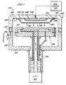
- Figure 1 is a cross sectional view of one embodiment of a chemical vapor deposition system 100.
- the system generally includes a chamber 102 coupled to a gas source 104.
- the chamber 102 has walls 106, a bottom 108 and a lid 110 that define a process volume 112.
- the walls 106 and bottom 108 are typically fabricated from a unitary block of aluminum.
- the chamber 100 contains a pumping ring 114 that couples the process volume 112 to an exhaust port 116 (that includes various pumping components not shown).
- the lid 110 is supported by the walls 106 and can be removed to service the chamber 102.
- the lid 110 is generally comprised of aluminum and may additionally contain heat transfer fluid channels for regulating the temperature of the lid 110 by flowing heat transfer fluid therethrough.
- a showerhead 118 is coupled to an interior side 120 of the lid 110.
- the showerhead 118 is typically fabricated from aluminum.
- the showerhead generally includes a perimeter mounting ring 122 that surrounds a "dish-shaped" center section 124.
- the mounting ring 122 includes a plurality of mounting holes 126 passing therethrough, each accepting a vented mounting screw 128 that threads into a mating hole 130 in the lid 110.
- the center section 124 includes a perforated area 132.
- a mixing block 134 is disposed in the lid 110.
- the mixing block 134 is coupled to the gas source 104 such that process and other gases may be introduced to the process volume 112 by passing through the mixing block 134 and showerhead 118.
- a blocker plate 136 disposed between the showerhead 118 and the mixing block 134 increases the uniform distribution of gases passing through the showerhead 118 into the chamber 102.
- a support assembly 138 is disposed beneath the showerhead 118.
- the support assembly 138 supports a substrate 140 during processing.
- the support assembly 138 is typically accessed by the substrate 140 through a port (not shown) in walls 106.
- the support assembly 138 is coupled to a lift system 144 that moves the support assembly 138 between an elevated position as shown and a lowered position.
- Bellows 146 provides a vacuum seal between the process volume 112 and the atmosphere outside the chamber 102 while facilitating the movement of the support assembly 138. Lift pins and the associated mechanisms have been omitted for clarity.
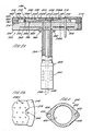
- Fig. 2A depicts the support assembly 138 in cross section.
- the scale of Fig. 2A has been exaggerated to clearly depict the features of the support assembly 138.
- the support assembly 138 generally includes a substrate support 202 and a stem 204.
- the substrate support 202 is comprised of a first (upper) plate 208 and a second (lower) plate 210.
- the upper plate 208 supports the substrate 140 during processing.
- the lower plate 210 generally has a first side 212 that is connected to the upper plate 208 and a second side 214 that is connected to the stem 204.
- the upper plate 208 and lower plate 210 are typically fused together, for example, by clamping the plates 208 and 210 together at an elevated temperature for a period of time, typically without a bonding agent.
- the plates may be coupled by sintering, adhesives, mechanical means ( i . e ., fasteners), and the like.
- the upper plate 208 is fabricated from ceramic, such as aluminum nitride. Preferably, about 95 percent pure aluminum nitride is used to enhance the thermal conductivity of the upper plate 208.
- the upper plate 208 includes a first or support surface 216 and a second surface 232A.
- the support surface 216 has a seal ring 218 that projects from the perimeter of the support surface 216.
- the seal ring 218 supports the substrate 140 at its perimeter and provides a seal therebetween to facilitate vacuum chucking of the substrate.
- the support surface 216 includes stepped surface 220 disposed radially inside the seal ring 218. In one embodiment, the stepped surface 220 includes a center portion 222, an intermediate portion 224 and an outer portion 226.
- the center portion 222 is orientated parallel to a plane defined by the seal ring 218.
- the intermediate portion 224 is orientated parallel to the center portion 222.
- the intermediate portion 224 is positioned between the center portion 222 and the seal ring 218.
- the outer portion 226 is orientated parallel to the center portion 222.
- the outer portion 226 is positioned between the intermediate portion 224 and the seal ring 218. Generally, 0.001 inches separate the planes defined by the portions 222, 224 and 226.
- a plurality of posts 228A, 228B and 228C are disposed on the stepped surface 220 (e.g., portions 222, 224 and 226).
- the posts 228A, 228B and 228C are typically integrally formed in the upper plate 208.
- the posts 228A are positioned in the center portion 222.
- the posts 228B are positioned in the intermediate portion 224 and the posts 228C are positioned in the outer portion 226.
- the posts 228A are slightly longer than the posts 228B and 228C.
- the posts 228B are slightly longer than the posts 228C.
- Each of the posts 228A, 228B and 228C includes a distal end 230 that lie in a common plane.
- the plane defined by the distal ends 230 may be substantially co-planar to the plane of the seal ring 218 such that the substrate is supported on the distal ends 230 of the posts 228A, 228B and 228C during processing without damaging the substrate by excessive flexing ( i.e ., bowing the substrate across the seal ring and posts).
- the stepped surface 220 provides a larger gap between the substrate and the center portion 222 to compensate for the tendency of the substrate to transfer heat to its center.
- the variable gap created between the substrate and the stepped surface 220 promotes better chucking effect for substrate 140 since size of caps and plural posts can be designed to attain better temperature uniformity.
- the temperature uniformity across the support assembly 138 can be within about 3 degrees Celsius.
- a vacuum port 250 is disposed through the upper plate 208.
- the vacuum port 250 has a varied cross section that includes an expanded portion 252 on the support surface 216 that has a generally larger cross sectional area relative the other portions of the vacuum port 250.
- the expanded portion 252 comprises a slot having a full radius at each end.
- the expanded portion 252 serves to decrease the pressure drop at the interface of the vacuum port 250 and support surface 216 during the application of the vacuum. This enhances temperature uniformity, and consequently deposition uniformity on the substrate 140.
- the expanded portion 252 may be configured in other geometries to accomplish the pressure reduction at the surface 216 disclosed herein.
- a channel 290 is formed between the upper and lower plates 208 and 210.
- the channel 290 provides a passage for purge gas through the substrate support 202 to a plenum 266 defined between a shadow ring 258 and the support 202.
- the purge gas flows from the plenum and over the edge of the substrate to prevent deposition at the substrate's edge.
- the channel 290 is formed in the upper plate 208.
- a portion or all of channel 290 may be disposed completely in the lower plate 210.
- some or all of the channel 290 may be disposed at least partially in the upper plate 208 and at least partially in the lower plate 210 or various combinations thereof.
- the mating of the surfaces of the upper and lower plates 208, 210 defines the channels 290 and confines travel of fluids thereto.
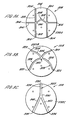
- Fig. 3A depicts one embodiment of the second surface 232A of the upper plate 208.
- the second surface 232A includes a plurality of channels 290 formed therein.
- the channels 290 are configured to fluidly couple a plurality of outlets 304 to a central origin 306.
- a fluid source (not shown) supplies a fluid (e . g ., purge gas) through the channels 290 from the central origin 306 to the outlets 304.
- a fluid e. g ., purge gas
- the geometry i.e ., cross sectional area
- each leg of the channel 290 will depend on the desired pressure at the outlets 304 downstream of the leg and the flow losses encountered therebetween.
- the flow losses include such factors such as the surface roughness and geometry of the leg, number of outlets 304 downstream of the leg, the length of each downstream leg, the flow properties of the fluid and the like.
- the channels 290 include a chevron-shaped primary channel 308 positioned offset from the center of the upper plate 208.
- the origin 306 is positioned at the mid-point of the chevron.
- Each end of the primary channel 308 branches into a first secondary channel 310, a second secondary channel 312 and a third secondary channel 314.
- the secondary channels 310, 312 and 314 couple the primary channel 308 to the outlets 304.
- the first secondary channel 310 and the secondary channel 312 are co-linearly orientated and have identical cross sections.
- the third secondary channel 314 is orientated substantially perpendicular to the first and second secondary channels 310, 312.
- the cross sectional area of the third secondary channel 314 is less than that of the first and second secondary channels 310, 312 to balance the flow of purge gas passing through the outlets 304.
- flow restrictors may be placed in the outlets 304 or elsewhere in the channel to balance the flow.
- outlets 304 may be positioned at varying distances about the second surface 232A.
- the flow of purge gas from the outlets 304 is desired to be non-uniform as to balance the flow of purge gas at the substrate's edge described further below.
- the flow of gas may be balanced by controlling the cross sections and lengths of the various channels as desired to tune the gas flow for the particular application.
- Fig. 3B depicts another embodiment of a second surface 232B of the upper plate 208.
- Channels 328 are formed in the second surface 232B of the upper plate 208 to distribute purge gas from a central origin 320 to a plurality of outlets 322.
- four outlets 322 are disposed equidistant about the perimeter of the second surface 232B.
- the outlets 322 that are closest to the central origin 320 have passages 324 disposed between the central origin and the respective outlets to provide a conduit for the purge gas.
- the outlets 322 that are farthest from the central origin 320 have passages 326 disposed between the central origin and the respective outlets to provide a conduit for the purge gas.
- the total flow restriction between the passages 324, 326 is balanced. Generally, this may be accomplished by having the cross sectional area of passages 326 greater than the cross sectional area of passages 324.
- Fig. 3C depicts yet another embodiment of a second surface 232C of the upper plate 208.
- Channels 342 are formed in the second surface 232C of the upper plate 208 to distribute purge gas from a central origin 330 to a plurality of outlets.
- three outlets 332, 334 and 336 are disposed at varying distances about the perimeter of the second surface 232B.
- the outlet 332 that is closest to the central origin 330 has a passage 338 disposed between the central origin and the outlet to provide a conduit for the purge gas.
- the outlets 334 and 336 that are farthest from the central origin 320 have passages 340 disposed between the central origin and the respective outlets to provide a conduit for the purge gas.
- the flow of purge gas through the outlet 322 must be greater than the flow through either of the outlets 334 and 336 to balance the purge gas flowing to the perimeter of the substrate. Generally, this may be accomplished by having the cross sectional area of passage 338 greater than the cross sectional area of passages 340.
- the lower plate 210 is fabricated from ceramic, such as aluminum nitride. Preferably, about 95 percent pure aluminum nitride is used to enhance the thermal conductivity of the lower plate 210.
- the lower plate 210 includes at least one heating element, such as an embedded electrode 234, having a first lead 236 and a second lead 238 extending out the second side 214 of the lower plate 210.
- the leads 236, 238 are coupled to a power source (not shown). The power source supplies power to the electrode 234 to enable the support 202 to heat the substrate 140 to a temperature up to about 300-550 degrees Celsius.
- the lower plate 210 additionally includes a vacuum passage 240, a purge passage 242 and a plurality of lift pin passages 244 extending therethrough.
- the lift pin passages 244 are generally disposed radially outwards from the vacuum passage 240 and the purge passage 242.
- the lift pin passages 244 extend from the lower plate 210 through upper plate 208, exiting the upper plate 208 through a tab 219 extending inwards and coplanar to the seal ring 218. (See Fig. 2B).
- the vacuum passage 240 and the purge passage 242 are generally positioned on opposing sides of the centerline of the lower plate 210.
- the lower plate 210 has a stepped perimeter 260 that extends beyond the first plate 208.
- the stepped perimeter 260 supports the shadow ring 258.
- the shadow ring 258 generally is annular in form and is comprised of ceramic such as aluminum nitride.
- the shadow ring 258 has a first side 270 and a second side 262.
- the first side 270 is supported by the perimeter 260.
- the second side 262 has a lip 264 extending radially inwards.
- the lip 264 and the lower plate 210 enclose the plenum 266 that receives the purge gas exiting the outlets 304.
- the purge gas is disposed about the perimeter of the substrate 140 through a gap 268 that communicates with the plenum 266 defined between the lip 264 and the upper plate 208.
- a clip assembly 272 is utilized to retain the ring 258 to the substrate support 202.
- An example of a clip assembly 272 is disclosed by Yudovsky in previously incorporated United States Patent Serial No. 09,504,288 (attorney docket no. 4501).
- the upper plate 208 and lower plate 210 are fused together.
- the plates 208 and 210 are sintered.
- the plates 208 and 210 should comprise similar materials (e.g., similar percentage of aluminum nitride) to minimize differences in thermal expansion.
- the fusing of the upper plate 208 and the lower plate 210 makes the channels 290 leak tight to about 1xE-9 sccs helium at 1xE-9 Torr differential.
- Fig. 4 depicts the stem 204 in cross section.
- the stem 204 generally is fabricated from ceramic, such as aluminum nitride. Typically about 99 percent pure aluminum nitride is preferred to minimize thermal transfer between the support 202 and stem 204.
- the stem 204 is generally tubular in cross section.
- the stem 204 has an annular section 402 that defines a central passage 404.
- a first projection 406 and a second projection 408 extend from the annular section 402.
- the first projection 406 has a purge gas passage 410 and the second projection 408 has a vacuum passage 412 respectively disposed therethrough.
- the thickness of the annular section 402 and the walls of the first and second projections 406, 408 are selected to minimize thermal conductivity therethrough.
- the stem 204 has a first end 246 and a second end 248.
- the first end 246 of the stem 204 is connected ( e.g ., fused, bonded or sintered) to the second side 214 of the lower plate 210.
- the leads 236, 238 pass through the central passage 404 of the stem 204 and are coupled to a power source (not shown).
- the union of the stem 204 and the lower plate 210 places the purge gas passage 410 disposed in the stem 204 in fluid communication with the purge gas passage 242 of the lower plate 210 and the channels 290 of the upper plate 208.
- Purge gas provided from a purge gas supply may be fed through the stem 204 and out the outlets 304 disposed in the substrate support 202 to minimize deposition at the substrate's edge.
- the union of the stem 204 and the lower plate 210 permits the vacuum passage 414 disposed in the stem 204 to be in fluid communication with the vacuum passage 240 of the lower plate 210 and the vacuum port 250 of the upper plate 208.
- a vacuum source (not shown) maintains a vacuum between the substrate 140 and the stepped surface 220 to retain the substrate 140 during processing by evacuating the volume between the substrate 140 and stepped surface 220 through the stem 204.
- the controlled cross section of the stem 204 minimizes the thermal transfer between the stem 204 and the substrate support 202.
- An isolator 254 is disposed at the second end 246 of the stem 204 to minimize the thermal transfer therefrom.
- the isolator 254 is typically comprised of a thermally insulative material compatible with the process environment such as a polymer.
- the isolator 254 comprises a polyimide, for example VESPEL® .
- a heat transfer block 256 couples the stem 204 to the lift system 144.
- the heat transfer block 256 is used to remove heat from the system 100.
- the fluid temperature can be specified to control ( i . e ., increase, maintain, or decrease) the heat transfer of shaft 204 to heat transfer block 256, to achieve required thermal uniformity of support 202.
- the heat transfer block 256 is generally a thermally conductive material such as aluminum. The heat transfer block 256 isolates the bellows 146 and lift system 144 from the high temperatures associated with the support assembly 138.
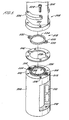
- Fig. 5 depicts an exploded view of the second end 248 of the stem 204, the insulator 254 and the heat transfer block 256.
- the base 248 of the stem 204 includes a plurality of mounting holes 520.
- a mounting screw 522 typically comprised of an alloy such as INCONEL® or HASTELLOY® , is passed through a clamp ring 524, the mounting hole 520 in the stem 204 and the insulator 254 and is threaded into a mating thread hole 526 in the heat transfer block 256.
- the clamp ring 524 may be separated into more than one part to facilitate assembly.
- the insulator 254 includes a patterned inner diameter 528 that accommodates the geometry of a seal 508 that is disposed between the heat transfer block 256 and the stem 204.
- the seal 508 is generally annular and comprised of a high temperature elastomer such as CHEMREZTM, KALBEZTM, KERREZTM, INTERNATIONAL SEAL.
- the seal 508 includes two integral tabs 530 extending from a center ring 534. Each tab 530 has an aperture 532 formed therethrough, communicating with passages 410 and 412.
- the heat transfer block 256 is generally annular in form having an axially centered passage 536.
- the heat transfer block 256 has a first surface 502 that has an outer projection 504 and an inner projection 506 extending therefrom.
- the projections 504 and 506 are configured to house the seal 508 therebetween.
- two bosses 512 may extend from the first surface 502 between the projections 504 and 506.
- the heat transfer block 256 additionally contains a purge gas passage 514 and a vacuum passage 516.
- the passages 514 and 516 extend through the heat transfer block 256 parallel to the centerline of the heat transfer block 256.
- the passages 514 and 516 exit the heat transfer block 256 through the bosses 512 and communicate with the passages 410 and 412, respectively, of the stem 204.
- the seal 508 prevents leakage at the junction of the passages 514 and 410, and passages 516 and 412.
- One or more passages 510 are disposed within the heat transfer block 256.
- the passages 510 are coupled to a fluid source (not shown).
- Heat transfer fluid such as de-ionized water, is passed through the passages 510 to regulate the temperature of the heat transfer block 256.
- the semiconductor substrate 140 depicted in Fig. 1 is secured to the support assembly 138 by providing a vacuum therebetween.
- the expanded portion 252 of the vacuum port 250 minimizes the local pressure drop and corresponding temperature change of gases being drawn into the vacuum port 250, thus preventing localized cooling on portion of the substrate directly above the vacuum port 250.
- the temperature of the substrate 140 is elevated to a predetermined process temperature primarily providing power to the electrode 234.
- the stepped surface 220 provides a variable gap that counters the tendency of the substrate 140 to have a higher temperature at the center of the substrate 140.
- the substrate 140 is heated to a steady state temperature. Using thermal control of both the lid 110 and the support assembly 138, the substrate 140 is maintained at a temperature of 300-550 degrees Celsius
- Gaseous components which in one embodiment may include silane and tungsten hexafluoride, are supplied from a gas panel to the process chamber through mixing block 134 and showerhead 118 to form a gaseous mixture.
- the gaseous mixture reacts to form a layer of tungsten on the substrate 140.
- purge gas is flowed into the plenum 266 from the channels 290, and distributed through the gap 268 between the shadow ring 258 and the support 202 to the perimeter of the substrate 140.
Landscapes
- Engineering & Computer Science (AREA)
- Chemical & Material Sciences (AREA)
- Computer Hardware Design (AREA)
- Condensed Matter Physics & Semiconductors (AREA)
- Power Engineering (AREA)
- Microelectronics & Electronic Packaging (AREA)
- Manufacturing & Machinery (AREA)
- General Physics & Mathematics (AREA)
- Physics & Mathematics (AREA)
- Metallurgy (AREA)
- Organic Chemistry (AREA)
- Chemical Kinetics & Catalysis (AREA)
- General Chemical & Material Sciences (AREA)
- Mechanical Engineering (AREA)
- Materials Engineering (AREA)
- Container, Conveyance, Adherence, Positioning, Of Wafer (AREA)
- Chemical Vapour Deposition (AREA)
Abstract
Description
- The invention relates generally to an apparatus for supporting a substrate in a semiconductor processing chamber.
- Integrated circuits have evolved into complex devices that can include millions of transistors, capacitors and resistors on a single chip. The evolution of chip designs continually requires faster circuitry and greater circuit density that demand increasingly precise fabrication processes. One fabrication process frequently used is chemical vapor deposition (CVD).
- Chemical vapor deposition is generally employed to deposit a thin film on a substrate or semiconductor wafer. Chemical vapor deposition is generally accomplished by introducing a precursor gas in to a vacuum chamber. The precursor gas is typically directed through a showerhead situated near the top of the chamber. The precursor gas reacts to form a layer of material on a surface of the substrate that is positioned on a heated substrate support. Purge gas is routed through holes in the support to the edge of the substrate to prevent deposition at the substrate's edge that may cause the substrate to adhere to the support. Volatile by-products produced during the reaction are pumped from the chamber through an exhaust system.
- One material frequently formed on substrates using a chemical vapor deposition process is tungsten. A precursor gas that may be used to form tungsten generally includes tungsten hexafluoride (WF6) and silane. As the silane and tungsten hexafluoride mix, some "stray" tungsten (i.e., tungsten that does not deposit on the substrate) deposits on the showerhead and other chamber components. The stray tungsten film builds on the showerhead and may become a source of contamination in the chamber. Eventually, the stray tungsten may clog the holes in the showerhead that facilitate the passage of the precursor gas therethrough necessitating the showerhead be removed and cleaned or replaced.
- To extend the interval in time between the routine maintenance of the showerhead, fluorine based chemistries are generally used to clean (i.e., etch away) the stray tungsten film. However, the use of fluorine, while advantageous for removing tungsten, reacts to form a layer of aluminum fluoride on the heated support that is commonly made of aluminum. The aluminum fluoride layer has a generally rough surface topography. The rough surface creates a leak path that impairs the vacuum used to chuck or hold the substrate to the heated support. Additionally, the aluminum fluoride layer is a potential source of particulate contamination.
- Substrate supports fabricated from ceramic materials provide an improvement over aluminum supports due to ceramic's resistance to fluorine. However, ceramic supports are difficult to fabricate. For example, the holes in ceramic support used to provide purge gas to the perimeter of the support are typically drilled from the perimeter of the support to a depth generally equal to the radius of the support. Drilling such a deep hole in ceramic is difficult. The tools used to make these holes are frequently broken during the fabrication (e.g., drilling) process. Broken tools disposed within the support must be removed or the support must be scrapped. These fabrication difficulties result in costly supports and an undesirable high scrap rate.
- Therefore, there is a need in the art for an improved heated support for chemical vapor deposition processes.
- One aspect of the present invention generally provides a substrate support assembly for supporting a substrate during processing. In one embodiment, a support assembly comprising a top ceramic plate having a first side, a bottom ceramic plate having a first side and an embedded electrode, the first side of the bottom plate fused to the first side of the top plate defining a channel therebetween is provided.
- In another embodiment, a support assembly includes a first plate having a first side and second side. A ring is disposed on the first side. A stepped surface is formed on the first side radially inward of the ring. A second plate is connected to the second side of the first plate.
- The teachings of the present invention can be readily understood by considering the following detailed description in conjunction with the accompanying drawings, in which:
- Fig. 1 depicts a schematic sectional view of one embodiment of a processing chamber of the present invention;
- Fig. 2A depicts a partial sectional view of a heater assembly;
- Fig. 2B depicts a partial plan view of the heater assembly;
- Fig. 3A depicts one embodiment of a surface of an upper plate;
- Fig. 3B depicts another embodiment of a surface of an upper plate;
- Fig. 3C depicts another embodiment of a surface of an upper plate;
- Fig. 4 depicts a cross section view of a stem; and
- Fig. 5 depicts an exploded view of a second end of the stem.
-
- To facilitate understanding, identical reference numerals have been used, where possible, to designate identical elements that are common to the figures.
- The present invention generally provides a processing system and heated substrate support that are advantageous for the deposition of tungsten films. The invention is illustratively described below as a chemical vapor deposition system, such as a WxZ™ metal chemical vapor deposition (MCVD) system, available from Applied Materials, Inc., of Santa Clara, California. However, it should be understood that the invention has utility when depositing other films and in other system configurations such as physical vapor deposition systems, chemical vapor deposition systems and any other system in which supporting a substrate on a ceramic support is desired.
- Figure 1 is a cross sectional view of one embodiment of a chemical
vapor deposition system 100. The system generally includes a chamber 102 coupled to agas source 104. The chamber 102 haswalls 106, abottom 108 and alid 110 that define aprocess volume 112. Thewalls 106 andbottom 108 are typically fabricated from a unitary block of aluminum. Thechamber 100 contains apumping ring 114 that couples theprocess volume 112 to an exhaust port 116 (that includes various pumping components not shown). - The
lid 110 is supported by thewalls 106 and can be removed to service the chamber 102. Thelid 110 is generally comprised of aluminum and may additionally contain heat transfer fluid channels for regulating the temperature of thelid 110 by flowing heat transfer fluid therethrough. - A
showerhead 118 is coupled to aninterior side 120 of thelid 110. Theshowerhead 118 is typically fabricated from aluminum. The showerhead generally includes aperimeter mounting ring 122 that surrounds a "dish-shaped"center section 124. Themounting ring 122 includes a plurality of mountingholes 126 passing therethrough, each accepting a ventedmounting screw 128 that threads into amating hole 130 in thelid 110. Thecenter section 124 includes a perforated area 132. - A
mixing block 134 is disposed in thelid 110. The mixingblock 134 is coupled to thegas source 104 such that process and other gases may be introduced to theprocess volume 112 by passing through the mixingblock 134 andshowerhead 118. Ablocker plate 136 disposed between theshowerhead 118 and themixing block 134 increases the uniform distribution of gases passing through theshowerhead 118 into the chamber 102. - A
support assembly 138 is disposed beneath theshowerhead 118. Thesupport assembly 138 supports a substrate 140 during processing. Thesupport assembly 138 is typically accessed by the substrate 140 through a port (not shown) inwalls 106. Generally, thesupport assembly 138 is coupled to a lift system 144 that moves thesupport assembly 138 between an elevated position as shown and a lowered position.Bellows 146 provides a vacuum seal between theprocess volume 112 and the atmosphere outside the chamber 102 while facilitating the movement of thesupport assembly 138. Lift pins and the associated mechanisms have been omitted for clarity. - Fig. 2A depicts the
support assembly 138 in cross section. The scale of Fig. 2A has been exaggerated to clearly depict the features of thesupport assembly 138. Thesupport assembly 138 generally includes asubstrate support 202 and astem 204. Thesubstrate support 202 is comprised of a first (upper)plate 208 and a second (lower)plate 210. Theupper plate 208 supports the substrate 140 during processing. Thelower plate 210 generally has afirst side 212 that is connected to theupper plate 208 and asecond side 214 that is connected to thestem 204. Theupper plate 208 andlower plate 210 are typically fused together, for example, by clamping theplates - The
upper plate 208 is fabricated from ceramic, such as aluminum nitride. Preferably, about 95 percent pure aluminum nitride is used to enhance the thermal conductivity of theupper plate 208. Theupper plate 208 includes a first orsupport surface 216 and asecond surface 232A. Thesupport surface 216 has aseal ring 218 that projects from the perimeter of thesupport surface 216. Theseal ring 218 supports the substrate 140 at its perimeter and provides a seal therebetween to facilitate vacuum chucking of the substrate. Thesupport surface 216 includes stepped surface 220 disposed radially inside theseal ring 218. In one embodiment, the stepped surface 220 includes acenter portion 222, anintermediate portion 224 and anouter portion 226. Thecenter portion 222 is orientated parallel to a plane defined by theseal ring 218. Theintermediate portion 224 is orientated parallel to thecenter portion 222. Theintermediate portion 224 is positioned between thecenter portion 222 and theseal ring 218. Theouter portion 226 is orientated parallel to thecenter portion 222. Theouter portion 226 is positioned between theintermediate portion 224 and theseal ring 218. Generally, 0.001 inches separate the planes defined by theportions - A plurality of
posts portions posts upper plate 208. The posts 228A are positioned in thecenter portion 222. Theposts 228B are positioned in theintermediate portion 224 and theposts 228C are positioned in theouter portion 226. The posts 228A are slightly longer than theposts posts 228B are slightly longer than theposts 228C. Each of theposts distal end 230 that lie in a common plane. The plane defined by the distal ends 230 may be substantially co-planar to the plane of theseal ring 218 such that the substrate is supported on the distal ends 230 of theposts - The stepped surface 220 provides a larger gap between the substrate and the
center portion 222 to compensate for the tendency of the substrate to transfer heat to its center. Thus, the variable gap created between the substrate and the stepped surface 220 promotes better chucking effect for substrate 140 since size of caps and plural posts can be designed to attain better temperature uniformity. For example, the temperature uniformity across thesupport assembly 138 can be within about 3 degrees Celsius. - A
vacuum port 250 is disposed through theupper plate 208. Thevacuum port 250 has a varied cross section that includes an expandedportion 252 on thesupport surface 216 that has a generally larger cross sectional area relative the other portions of thevacuum port 250. In one embodiment, the expandedportion 252 comprises a slot having a full radius at each end. The expandedportion 252 serves to decrease the pressure drop at the interface of thevacuum port 250 andsupport surface 216 during the application of the vacuum. This enhances temperature uniformity, and consequently deposition uniformity on the substrate 140. One skilled in the art will readily identify that the expandedportion 252 may be configured in other geometries to accomplish the pressure reduction at thesurface 216 disclosed herein. - A
channel 290 is formed between the upper andlower plates channel 290 provides a passage for purge gas through thesubstrate support 202 to aplenum 266 defined between ashadow ring 258 and thesupport 202. The purge gas flows from the plenum and over the edge of the substrate to prevent deposition at the substrate's edge. - Typically, the
channel 290 is formed in theupper plate 208. Optionally, a portion or all ofchannel 290 may be disposed completely in thelower plate 210. Optionally, some or all of thechannel 290 may be disposed at least partially in theupper plate 208 and at least partially in thelower plate 210 or various combinations thereof. Common to these embodiments is that the mating of the surfaces of the upper andlower plates channels 290 and confines travel of fluids thereto. - Fig. 3A depicts one embodiment of the
second surface 232A of theupper plate 208. In one embodiment, thesecond surface 232A includes a plurality ofchannels 290 formed therein. Thechannels 290 are configured to fluidly couple a plurality ofoutlets 304 to acentral origin 306. A fluid source (not shown) supplies a fluid (e.g., purge gas) through thechannels 290 from thecentral origin 306 to theoutlets 304. As it is preferable to maintain substantially the same pressures at eachoutlet 304 when the outlets are spaced equidistantly about the perimeter of thesecond surface 232A, the geometry (i.e., cross sectional area) is tuned for each "leg" of thechannels 290 to achieve this goal. As one skilled in the art will appreciate, the cross section of each leg of thechannel 290 will depend on the desired pressure at theoutlets 304 downstream of the leg and the flow losses encountered therebetween. The flow losses include such factors such as the surface roughness and geometry of the leg, number ofoutlets 304 downstream of the leg, the length of each downstream leg, the flow properties of the fluid and the like. - In the exemplary embodiment, the
channels 290 include a chevron-shapedprimary channel 308 positioned offset from the center of theupper plate 208. Theorigin 306 is positioned at the mid-point of the chevron. Each end of theprimary channel 308 branches into a first secondary channel 310, a secondsecondary channel 312 and a thirdsecondary channel 314. Thesecondary channels primary channel 308 to theoutlets 304. The first secondary channel 310 and thesecondary channel 312 are co-linearly orientated and have identical cross sections. The thirdsecondary channel 314 is orientated substantially perpendicular to the first and secondsecondary channels 310, 312. As the thirdsecondary channel 314 is shorter in length than the first and secondsecondary channels 310, 312, the cross sectional area of the thirdsecondary channel 314 is less than that of the first and secondsecondary channels 310, 312 to balance the flow of purge gas passing through theoutlets 304. Optionally, flow restrictors may be placed in theoutlets 304 or elsewhere in the channel to balance the flow. - Alternatively, the
outlets 304 may be positioned at varying distances about thesecond surface 232A. In such an orientation, the flow of purge gas from theoutlets 304 is desired to be non-uniform as to balance the flow of purge gas at the substrate's edge described further below. The flow of gas may be balanced by controlling the cross sections and lengths of the various channels as desired to tune the gas flow for the particular application. - Fig. 3B depicts another embodiment of a
second surface 232B of theupper plate 208.Channels 328 are formed in thesecond surface 232B of theupper plate 208 to distribute purge gas from acentral origin 320 to a plurality ofoutlets 322. In one embodiment, fouroutlets 322 are disposed equidistant about the perimeter of thesecond surface 232B. Theoutlets 322 that are closest to thecentral origin 320 havepassages 324 disposed between the central origin and the respective outlets to provide a conduit for the purge gas. Theoutlets 322 that are farthest from thecentral origin 320 havepassages 326 disposed between the central origin and the respective outlets to provide a conduit for the purge gas. To provide a uniform distribution of purge gas to the perimeter of thesecond surface 232B, the total flow restriction between thepassages passages 326 greater than the cross sectional area ofpassages 324. - Fig. 3C depicts yet another embodiment of a
second surface 232C of theupper plate 208.Channels 342 are formed in thesecond surface 232C of theupper plate 208 to distribute purge gas from acentral origin 330 to a plurality of outlets. In one embodiment, threeoutlets second surface 232B. Theoutlet 332 that is closest to thecentral origin 330 has apassage 338 disposed between the central origin and the outlet to provide a conduit for the purge gas. Theoutlets central origin 320 havepassages 340 disposed between the central origin and the respective outlets to provide a conduit for the purge gas. To provide a uniform distribution of purge gas around the substrate, the flow of purge gas through theoutlet 322 must be greater than the flow through either of theoutlets passage 338 greater than the cross sectional area ofpassages 340. - Returning to Fig. 2A, the
lower plate 210 is fabricated from ceramic, such as aluminum nitride. Preferably, about 95 percent pure aluminum nitride is used to enhance the thermal conductivity of thelower plate 210. Thelower plate 210 includes at least one heating element, such as an embeddedelectrode 234, having afirst lead 236 and asecond lead 238 extending out thesecond side 214 of thelower plate 210. The leads 236, 238 are coupled to a power source (not shown). The power source supplies power to theelectrode 234 to enable thesupport 202 to heat the substrate 140 to a temperature up to about 300-550 degrees Celsius. - The
lower plate 210 additionally includes avacuum passage 240, apurge passage 242 and a plurality oflift pin passages 244 extending therethrough. Thelift pin passages 244 are generally disposed radially outwards from thevacuum passage 240 and thepurge passage 242. Thelift pin passages 244 extend from thelower plate 210 throughupper plate 208, exiting theupper plate 208 through a tab 219 extending inwards and coplanar to theseal ring 218. (See Fig. 2B). Thevacuum passage 240 and thepurge passage 242 are generally positioned on opposing sides of the centerline of thelower plate 210. - The
lower plate 210 has a steppedperimeter 260 that extends beyond thefirst plate 208. The steppedperimeter 260 supports theshadow ring 258. Theshadow ring 258 generally is annular in form and is comprised of ceramic such as aluminum nitride. Theshadow ring 258 has afirst side 270 and asecond side 262. Thefirst side 270 is supported by theperimeter 260. Thesecond side 262 has alip 264 extending radially inwards. Thelip 264 and thelower plate 210 enclose theplenum 266 that receives the purge gas exiting theoutlets 304. The purge gas is disposed about the perimeter of the substrate 140 through agap 268 that communicates with theplenum 266 defined between thelip 264 and theupper plate 208. Aclip assembly 272 is utilized to retain thering 258 to thesubstrate support 202. An example of aclip assembly 272 is disclosed by Yudovsky in previously incorporated United States Patent Serial No. 09,504,288 (attorney docket no. 4501). - The
upper plate 208 andlower plate 210 are fused together. In one embodiment, theplates plates upper plate 208 and thelower plate 210 makes thechannels 290 leak tight to about 1xE-9 sccs helium at 1xE-9 Torr differential. - Fig. 4 depicts the
stem 204 in cross section. Thestem 204 generally is fabricated from ceramic, such as aluminum nitride. Typically about 99 percent pure aluminum nitride is preferred to minimize thermal transfer between thesupport 202 andstem 204. Thestem 204 is generally tubular in cross section. Thestem 204 has anannular section 402 that defines acentral passage 404. Afirst projection 406 and a second projection 408 extend from theannular section 402. Thefirst projection 406 has apurge gas passage 410 and the second projection 408 has avacuum passage 412 respectively disposed therethrough. The thickness of theannular section 402 and the walls of the first andsecond projections 406, 408 are selected to minimize thermal conductivity therethrough. - Returning to Fig. 2A, the
stem 204 has afirst end 246 and asecond end 248. Thefirst end 246 of thestem 204 is connected (e.g., fused, bonded or sintered) to thesecond side 214 of thelower plate 210. The leads 236, 238 pass through thecentral passage 404 of thestem 204 and are coupled to a power source (not shown). The union of thestem 204 and thelower plate 210 places thepurge gas passage 410 disposed in thestem 204 in fluid communication with thepurge gas passage 242 of thelower plate 210 and thechannels 290 of theupper plate 208. Purge gas provided from a purge gas supply (not shown) may be fed through thestem 204 and out theoutlets 304 disposed in thesubstrate support 202 to minimize deposition at the substrate's edge. Similarly, the union of thestem 204 and thelower plate 210 permits the vacuum passage 414 disposed in thestem 204 to be in fluid communication with thevacuum passage 240 of thelower plate 210 and thevacuum port 250 of theupper plate 208. A vacuum source (not shown) maintains a vacuum between the substrate 140 and the stepped surface 220 to retain the substrate 140 during processing by evacuating the volume between the substrate 140 and stepped surface 220 through thestem 204. The controlled cross section of thestem 204 minimizes the thermal transfer between thestem 204 and thesubstrate support 202. - An isolator 254 is disposed at the
second end 246 of thestem 204 to minimize the thermal transfer therefrom. The isolator 254 is typically comprised of a thermally insulative material compatible with the process environment such as a polymer. In one embodiment, the isolator 254 comprises a polyimide, for example VESPEL® . - A heat transfer block 256 couples the
stem 204 to the lift system 144. Generally, theheat transfer block 256 is used to remove heat from thesystem 100. The fluid temperature can be specified to control (i.e., increase, maintain, or decrease) the heat transfer ofshaft 204 to heattransfer block 256, to achieve required thermal uniformity ofsupport 202. Theheat transfer block 256 is generally a thermally conductive material such as aluminum. Theheat transfer block 256 isolates thebellows 146 and lift system 144 from the high temperatures associated with thesupport assembly 138. - Fig. 5 depicts an exploded view of the
second end 248 of thestem 204, the insulator 254 and theheat transfer block 256. Thebase 248 of thestem 204 includes a plurality of mountingholes 520. A mountingscrew 522, typically comprised of an alloy such as INCONEL® or HASTELLOY® , is passed through aclamp ring 524, the mountinghole 520 in thestem 204 and the insulator 254 and is threaded into amating thread hole 526 in theheat transfer block 256. Theclamp ring 524 may be separated into more than one part to facilitate assembly. - The insulator 254 includes a patterned inner diameter 528 that accommodates the geometry of a
seal 508 that is disposed between theheat transfer block 256 and thestem 204. Theseal 508 is generally annular and comprised of a high temperature elastomer such as CHEMREZ™, KALBEZ™, KERREZ™, INTERNATIONAL SEAL. Theseal 508 includes twointegral tabs 530 extending from acenter ring 534. Eachtab 530 has anaperture 532 formed therethrough, communicating withpassages - The
heat transfer block 256 is generally annular in form having an axially centeredpassage 536. Theheat transfer block 256 has afirst surface 502 that has anouter projection 504 and aninner projection 506 extending therefrom. Theprojections seal 508 therebetween. Optionally, twobosses 512 may extend from thefirst surface 502 between theprojections - The
heat transfer block 256 additionally contains apurge gas passage 514 and avacuum passage 516. Thepassages heat transfer block 256 parallel to the centerline of theheat transfer block 256. Thepassages heat transfer block 256 through thebosses 512 and communicate with thepassages stem 204. Theseal 508 prevents leakage at the junction of thepassages passages - One or
more passages 510 are disposed within theheat transfer block 256. Thepassages 510 are coupled to a fluid source (not shown). Heat transfer fluid, such as de-ionized water, is passed through thepassages 510 to regulate the temperature of theheat transfer block 256. Theseal 508, being substantially enclosed by theprojections bosses 512 of theheat transfer block 256, is generally protected from heat propagated through thestem 204 from thesubstrate support 202 by controlling the temperature of theheat transfer block 256. - In operation, the semiconductor substrate 140 depicted in Fig. 1 is secured to the
support assembly 138 by providing a vacuum therebetween. The expandedportion 252 of thevacuum port 250 minimizes the local pressure drop and corresponding temperature change of gases being drawn into thevacuum port 250, thus preventing localized cooling on portion of the substrate directly above thevacuum port 250. - The temperature of the substrate 140 is elevated to a predetermined process temperature primarily providing power to the
electrode 234. The stepped surface 220 provides a variable gap that counters the tendency of the substrate 140 to have a higher temperature at the center of the substrate 140. During the deposition process, the substrate 140 is heated to a steady state temperature. Using thermal control of both thelid 110 and thesupport assembly 138, the substrate 140 is maintained at a temperature of 300-550 degrees Celsius - Gaseous components, which in one embodiment may include silane and tungsten hexafluoride, are supplied from a gas panel to the process chamber through mixing
block 134 and showerhead 118 to form a gaseous mixture. The gaseous mixture reacts to form a layer of tungsten on the substrate 140. To prevent deposition at the substrate's edge and possible adherence of substrate 140 to thesupport assembly 138, purge gas is flowed into theplenum 266 from thechannels 290, and distributed through thegap 268 between theshadow ring 258 and thesupport 202 to the perimeter of the substrate 140. - Although the teachings of the present invention that have been shown and described in detail herein, those skilled in the art can readily devise other varied embodiments that still incorporate the teachings and do not depart from the scope and spirit of the invention.
Claims (34)
- A support assembly for supporting a workpiece comprising:a first ceramic plate having a first side;a second plate having a first side and an embedded electrode, the first side of the second plate connected to the first side of the first plate; anda channel defined between the first side of the first plate and the first side of the second plate.
- A support assembly as claimed in claim 1, wherein the channel is at least partially defined in the first plate.
- A support assembly as claimed in claim 1, wherein the channel is
at least partially defined in the second plate - A support assembly as claimed in any of claims 1 to 3, wherein the second plate further comprises:
a hole disposed through the second plate in communication with the channel. - A support assembly as claimed in claim 4, wherein the channel further comprises a plurality of passages, each passage coupling the central origin with an outlet.
- A support assembly as claimed in claim 5, wherein the passages comprises:one or more shorter passages; andone or more longer passages having a cross section greater than the shorter passages.
- A support assembly as claimed in claim 5 or claim 6, wherein the channel and outlets are disposed in the second plate.
- A support assembly as claimed in any of claims 5 to 7, wherein at least one of the outlets further comprises a flow restrictor disposed therein.
- A support assembly as claimed in any of claims 5 to 8, wherein the channel further comprises:a primary channel having a mid-point coinciding with the central origin; anda first secondary channel, a second secondary channel and a third secondary channel branching from each end of the primary channel, the first secondary channel, the second secondary channel and the third secondary channel each coupling the primary channel to the outlets.
- A support assembly as claimed in any of claims 1 to 9, wherein the first plate further comprises:a second surface adapted to support the substrate; anda vacuum port disposed at least partially in the second surface.
- A support assembly as claimed in any of claims 1 to 9, wherein the first plate further comprises:a second surface adapted to support the substrate;a vacuum port disposed through the first plate; andan enlarged portion of the vacuum port disposed at least partially in the second surface.
- A support assembly as claimed in any of claims 1 to 11, wherein the first plate further comprises:
a stepped surface disposed opposite the first side of the first plate. - A support assembly as claimed in claim 12, wherein the stepped surface further comprises:
a center portion, an intermediate portion and an outer portion, wherein a center portion extends farthest below the first side of the first plate. - A support assembly as claimed in claim 12 or claim 13, wherein the stepped surface further comprises:an outer portion;an intermediate portion that extends 0.001 inches from the outer portion; anda center portion that extends 0.001 inches from the intermediate portion.
- A support assembly as claimed in any of claims 12 to 14, wherein the stepped surface further comprises:
a plurality of posts extending therefrom. - A support assembly as claimed in claim 1 to 15, wherein the second plate further comprise aluminum nitride.
- A support assembly as claimed in any of claims 1 to 16, further comprising:
a ceramic stem connected to the second plate. - A support assembly as claimed in claim 17, wherein the stem further comprises:a central, axial passage;a first gas passage disposed coaxial to the central passage; anda second gas passage disposed coaxial to the central passage.
- A support assembly as claimed in claim 17 or claim 18, wherein the stem further comprises:a central, axial passage;a first gas passage disposed coaxial to the central passage; anda second gas passage disposed coaxial to the first gas passage, the second gas passage and the first gas passage on opposite sides of the central passage.
- A support assembly as claimed in any of claims 1 to 19 further comprising:a ceramic stem having a first end and a second end; the first end fused to the second plate; anda heat transfer block disposed coupled to the second end.
- A support assembly as claimed in claim 20, wherein the heat transfer block further comprises:a first surface having a plurality of projections; anda seal disposed between the projections.
- A support assembly as claimed in claim 21, further comprising:
an insulator disposed between the heat transfer block and the stem. - A support assembly as claimed in any of claims 20 to 22, wherein the heat transfer block further comprises:
a plurality of heat transfer passages disposed therein. - A support assembly as claimed in any of claims 1 to 23, wherein the first plate further comprises:a center portion, an intermediate portion, and an outer portion defining a stepped surface adapted to support the substrate, wherein a center portion extends farthest below the first side of the first plate;a plurality of posts extending from the stepped surface;a vacuum port disposed through the first plate; an enlarged portion of the vacuum port disposed in the center portion.
- A support assembly as claimed in any of claims 1 to 24, further comprising:a ring disposed on the second plate; anda plenum defined between the ring and the first plate, the plenum in communication with the channels.
- A support assembly for supporting a workpiece comprising:a first plate having a first side and second side;a ring disposed on the first side;a stepped surface formed on the first side radially inwards of the ring; anda second plate connected to the second side of the first plate.
- A support assembly as claimed in claim 26 further comprising:
a channel defined between the first side of the first plate and the second side of the second plate. - A support assembly as claimed in claim 26 further comprising:
a heater embedded in the second plate. - A support assembly as claimed in any of claims 26 to 28, further comprising:
a plurality of posts extending from the stepped surface; each post having a distal end substantially coplanar with the ring. - A support assembly as claimed in any of claims 26 to 29, wherein the stepped surface further comprises:
a center portion, an intermediate portion and an outer portion, wherein a center portion extends farthest below the first side of the first plate. - A support assembly as claimed in claim 30, wherein the stepped surface further comprises:an outer portion;an intermediate portion that extends 0.001 inches from the outer portion; anda center portion that extends 0.001 inches from the intermediate portion.
- A support assembly for supporting a workpiece comprising:a first ceramic plate having a first side;a second ceramic plate having a first side and an embedded electrode, the first side of the second plate fused to the first side of the first plate;a channel defined between the first side of the first plate and the second side of the second plate;a ceramic stem fused to the second plate having a center passage, a purge gas passage and a vacuum passage; anda cooling block coupled to the stem.
- A semiconductor process chamber comprising:a chamber having sidewalls and a lid defining a process volume;a first ceramic plate having a first side disposed in the process volume;a second ceramic plate having a first side and an embedded electrode, the first side of the second plate fused to the first side of the first plate;a channel defined between the first side of the first plate and the second side of the second plate;a ceramic stem fused to the second plate having a center passage, a purge gas passage and a vacuum passage; anda cooling block coupled to the stem.
- A semiconductor process chamber as claimed in claim 33, wherein the chamber is a chemical vapor deposition chamber.
Applications Claiming Priority (2)
| Application Number | Priority Date | Filing Date | Title |
|---|---|---|---|
| US596854 | 1990-10-12 | ||
| US09/596,854 US6494955B1 (en) | 2000-02-15 | 2000-06-19 | Ceramic substrate support |
Publications (1)
| Publication Number | Publication Date |
|---|---|
| EP1167573A1 true EP1167573A1 (en) | 2002-01-02 |
Family
ID=24388994
Family Applications (1)
| Application Number | Title | Priority Date | Filing Date |
|---|---|---|---|
| EP01305217A Withdrawn EP1167573A1 (en) | 2000-06-19 | 2001-06-15 | Substrate support for a semiconductor processing chamber |
Country Status (4)
| Country | Link |
|---|---|
| US (1) | US6494955B1 (en) |
| EP (1) | EP1167573A1 (en) |
| JP (2) | JP5301065B2 (en) |
| KR (1) | KR20010113558A (en) |
Cited By (9)
| Publication number | Priority date | Publication date | Assignee | Title |
|---|---|---|---|---|
| DE10261362A1 (en) * | 2002-12-30 | 2004-07-15 | Osram Opto Semiconductors Gmbh | Semiconductor substrate holder for epitaxial processes, has structure designed to equalize temperature over substrate placed on or near it |
| EP1528589A2 (en) * | 2003-10-31 | 2005-05-04 | Tokyo Electron Limited | Stage for placing target object |
| US7252737B2 (en) * | 2001-08-09 | 2007-08-07 | Applied Materials, Inc. | Pedestal with integral shield |
| EP1703546A3 (en) * | 2005-03-16 | 2008-09-03 | Ngk Insulators, Ltd. | Processing device |
| EP1703545A3 (en) * | 2005-03-16 | 2009-02-18 | Ngk Insulators, Ltd. | Gas providing member and processing device |
| US10684554B2 (en) | 2005-05-03 | 2020-06-16 | Asml Netherlands B.V. | Lithographic apparatus and device manufacturing method |
| US10747126B2 (en) | 2011-08-17 | 2020-08-18 | Asml Netherlands B.V. | Support table for a lithographic apparatus, lithographic apparatus and device manufacturing method |
| US10788755B2 (en) | 2002-11-12 | 2020-09-29 | Asml Netherlands B.V. | Lithographic apparatus and device manufacturing method |
| WO2023163783A1 (en) * | 2022-02-22 | 2023-08-31 | Applied Materials, Inc. | Pocket heater with purge to improve gap tolerance |
Families Citing this family (46)
| Publication number | Priority date | Publication date | Assignee | Title |
|---|---|---|---|---|
| US5873781A (en) * | 1996-11-14 | 1999-02-23 | Bally Gaming International, Inc. | Gaming machine having truly random results |
| JP4009100B2 (en) * | 2000-12-28 | 2007-11-14 | 東京エレクトロン株式会社 | Substrate heating apparatus and substrate heating method |
| KR100792691B1 (en) * | 2001-06-14 | 2008-01-09 | 리버 벨 가부시키가이샤 | Wafer conveying machine |
| US20030173346A1 (en) * | 2002-03-18 | 2003-09-18 | Renken Wayne Glenn | System and method for heating and cooling wafer at accelerated rates |
| JP4034096B2 (en) * | 2002-03-19 | 2008-01-16 | 日本碍子株式会社 | Semiconductor support equipment |
| US20040011780A1 (en) * | 2002-07-22 | 2004-01-22 | Applied Materials, Inc. | Method for achieving a desired process uniformity by modifying surface topography of substrate heater |
| TWI220786B (en) * | 2002-09-11 | 2004-09-01 | Au Optronics Corp | Supporting structure |
| JP4060684B2 (en) * | 2002-10-29 | 2008-03-12 | 日本発条株式会社 | stage |
| JP4647595B2 (en) * | 2004-02-25 | 2011-03-09 | Jx日鉱日石金属株式会社 | Vapor growth equipment |
| US20060054090A1 (en) * | 2004-09-15 | 2006-03-16 | Applied Materials, Inc. | PECVD susceptor support construction |
| JP4783213B2 (en) * | 2005-06-09 | 2011-09-28 | 日本碍子株式会社 | Electrostatic chuck |
| TW200711029A (en) * | 2005-08-05 | 2007-03-16 | Tokyo Electron Ltd | Substrate processing apparatus and substrate stage used therein |
| JP2007046141A (en) * | 2005-08-12 | 2007-02-22 | Ngk Insulators Ltd | Heating device |
| JP2007051317A (en) * | 2005-08-16 | 2007-03-01 | Ngk Insulators Ltd | Heating device |
| KR20070118782A (en) * | 2006-06-13 | 2007-12-18 | 주식회사 아이피에스 | Waferblock |
| JP5111876B2 (en) * | 2007-01-31 | 2013-01-09 | 東京エレクトロン株式会社 | Substrate mounting structure and substrate processing apparatus |
| JP5179482B2 (en) * | 2007-05-09 | 2013-04-10 | 株式会社アルバック | Purge gas assembly |
| KR101418989B1 (en) * | 2008-06-16 | 2014-07-11 | 주식회사 원익아이피에스 | Substrate supporting device for vacuum processing apparatus, vacuum processing apparatus having same, and method for examining breakage of substrate |
| CN102341902A (en) * | 2009-03-03 | 2012-02-01 | 东京毅力科创株式会社 | Placing table structure, film forming apparatus, and raw material recovery method |
| JP5656392B2 (en) * | 2009-11-27 | 2015-01-21 | キヤノン株式会社 | Substrate holding apparatus, exposure apparatus using the same, and device manufacturing method |
| US9490150B2 (en) * | 2012-07-03 | 2016-11-08 | Applied Materials, Inc. | Substrate support for substrate backside contamination control |
| US8865602B2 (en) | 2012-09-28 | 2014-10-21 | Applied Materials, Inc. | Edge ring lip |
| KR101923050B1 (en) | 2012-10-24 | 2018-11-29 | 어플라이드 머티어리얼스, 인코포레이티드 | Minimal contact edge ring for rapid thermal processing |
| US9543186B2 (en) * | 2013-02-01 | 2017-01-10 | Applied Materials, Inc. | Substrate support with controlled sealing gap |
| US9916994B2 (en) | 2013-03-06 | 2018-03-13 | Applied Materials, Inc. | Substrate support with multi-piece sealing surface |
| US9991153B2 (en) * | 2013-03-14 | 2018-06-05 | Applied Materials, Inc. | Substrate support bushing |
| US20150194326A1 (en) * | 2014-01-07 | 2015-07-09 | Applied Materials, Inc. | Pecvd ceramic heater with wide range of operating temperatures |
| JP2015195259A (en) * | 2014-03-31 | 2015-11-05 | 豊田合成株式会社 | Susceptor and vapor phase growth device |
| US20160002778A1 (en) * | 2014-07-03 | 2016-01-07 | Applied Materials, Inc. | Substrate support with more uniform edge purge |
| US10497606B2 (en) * | 2015-02-09 | 2019-12-03 | Applied Materials, Inc. | Dual-zone heater for plasma processing |
| US10153133B2 (en) | 2015-03-23 | 2018-12-11 | Applied Materials, Inc. | Plasma reactor having digital control over rotation frequency of a microwave field with direct up-conversion |
| US10177024B2 (en) * | 2015-05-12 | 2019-01-08 | Lam Research Corporation | High temperature substrate pedestal module and components thereof |
| US9738975B2 (en) * | 2015-05-12 | 2017-08-22 | Lam Research Corporation | Substrate pedestal module including backside gas delivery tube and method of making |
| KR102507283B1 (en) | 2015-12-22 | 2023-03-07 | 삼성전자주식회사 | A substrate chuck and a substrate bonding system including the same |
| KR102523850B1 (en) * | 2016-07-11 | 2023-04-21 | 주식회사 미코세라믹스 | Chuck structure and apparatus for separating chips having the chuck structure |
| US10147610B1 (en) | 2017-05-30 | 2018-12-04 | Lam Research Corporation | Substrate pedestal module including metallized ceramic tubes for RF and gas delivery |
| CN110010517B (en) | 2017-11-27 | 2022-01-04 | 台湾积体电路制造股份有限公司 | Heating stage and apparatus for processing semiconductor wafers |
| WO2019187785A1 (en) * | 2018-03-26 | 2019-10-03 | 日本碍子株式会社 | Electrostatic chuck heater |
| WO2019240891A1 (en) | 2018-06-15 | 2019-12-19 | Mattson Technology, Inc. | Methods and apparatus for post exposure bake processing of a workpiece |
| WO2020149936A1 (en) * | 2019-01-18 | 2020-07-23 | Applied Materials, Inc. | Heated pedestal design for improved heat transfer and temperature uniformity |
| JP7145990B2 (en) * | 2020-03-31 | 2022-10-03 | 芝浦メカトロニクス株式会社 | Substrate processing equipment |
| US20220351951A1 (en) * | 2021-04-29 | 2022-11-03 | Applied Materials, Inc. | Substrate support apparatus, methods, and systems having elevated surfaces for heat transfer |
| US20220367236A1 (en) * | 2021-05-16 | 2022-11-17 | Applied Materials, Inc. | Heater pedestal with improved uniformity |
| US11869795B2 (en) | 2021-07-09 | 2024-01-09 | Applied Materials, Inc. | Mesa height modulation for thickness correction |
| JP7409535B1 (en) | 2023-02-22 | 2024-01-09 | Toto株式会社 | Electrostatic chuck and its manufacturing method |
| JP7409536B1 (en) | 2023-02-22 | 2024-01-09 | Toto株式会社 | Electrostatic chuck and its manufacturing method |
Citations (4)
| Publication number | Priority date | Publication date | Assignee | Title |
|---|---|---|---|---|
| US5242501A (en) * | 1982-09-10 | 1993-09-07 | Lam Research Corporation | Susceptor in chemical vapor deposition reactors |
| US5306895A (en) * | 1991-03-26 | 1994-04-26 | Ngk Insulators, Ltd. | Corrosion-resistant member for chemical apparatus using halogen series corrosive gas |
| US5688331A (en) * | 1993-05-27 | 1997-11-18 | Applied Materisls, Inc. | Resistance heated stem mounted aluminum susceptor assembly |
| US6045862A (en) * | 1997-07-16 | 2000-04-04 | Tokyo Electron Limited | CVD film forming method in which a film formation preventing gas is supplied in a direction from a rear surface of an object to be processed |
Family Cites Families (32)
| Publication number | Priority date | Publication date | Assignee | Title |
|---|---|---|---|---|
| US4997677A (en) * | 1987-08-31 | 1991-03-05 | Massachusetts Institute Of Technology | Vapor phase reactor for making multilayer structures |
| US5620525A (en) * | 1990-07-16 | 1997-04-15 | Novellus Systems, Inc. | Apparatus for supporting a substrate and introducing gas flow doximate to an edge of the substrate |
| US5280156A (en) | 1990-12-25 | 1994-01-18 | Ngk Insulators, Ltd. | Wafer heating apparatus and with ceramic substrate and dielectric layer having electrostatic chucking means |
| US5155652A (en) | 1991-05-02 | 1992-10-13 | International Business Machines Corporation | Temperature cycling ceramic electrostatic chuck |
| US5207437A (en) * | 1991-10-29 | 1993-05-04 | International Business Machines Corporation | Ceramic electrostatic wafer chuck |
| JP2603909B2 (en) * | 1992-06-24 | 1997-04-23 | アネルバ株式会社 | CVD apparatus, multi-chamber type CVD apparatus and substrate processing method thereof |
| JP3024940B2 (en) * | 1992-06-24 | 2000-03-27 | アネルバ株式会社 | Substrate processing method and CVD processing method |
| US5534072A (en) | 1992-06-24 | 1996-07-09 | Anelva Corporation | Integrated module multi-chamber CVD processing system and its method for processing subtrates |
| US5800686A (en) | 1993-04-05 | 1998-09-01 | Applied Materials, Inc. | Chemical vapor deposition chamber with substrate edge protection |
| JP3165938B2 (en) | 1993-06-24 | 2001-05-14 | 東京エレクトロン株式会社 | Gas treatment equipment |
| JPH07307377A (en) | 1993-12-27 | 1995-11-21 | Shin Etsu Chem Co Ltd | Ceramic heater with electrostatic chuck |
| EP0668607A1 (en) | 1994-02-22 | 1995-08-23 | Applied Materials, Inc. | Erosion resistant electrostatic chuck |
| EP0746874A1 (en) * | 1994-02-23 | 1996-12-11 | Applied Materials, Inc. | Chemical vapor deposition chamber |
| US5766365A (en) * | 1994-02-23 | 1998-06-16 | Applied Materials, Inc. | Removable ring for controlling edge deposition in substrate processing apparatus |
| US5581874A (en) | 1994-03-28 | 1996-12-10 | Tokyo Electron Limited | Method of forming a bonding portion |
| JPH07280462A (en) | 1994-04-11 | 1995-10-27 | Shin Etsu Chem Co Ltd | Soaking ceramic heater |
| US5476548A (en) | 1994-06-20 | 1995-12-19 | Applied Materials, Inc. | Reducing backside deposition in a substrate processing apparatus through the use of a shadow ring |
| JP2783980B2 (en) | 1994-09-01 | 1998-08-06 | 日本碍子株式会社 | Joint body and method of manufacturing the same |
| JPH08302474A (en) | 1995-04-28 | 1996-11-19 | Anelva Corp | Heater for cvd apparatus |
| US5886863A (en) | 1995-05-09 | 1999-03-23 | Kyocera Corporation | Wafer support member |
| JP3599204B2 (en) | 1995-06-08 | 2004-12-08 | アネルバ株式会社 | CVD equipment |
| US6053982A (en) * | 1995-09-01 | 2000-04-25 | Asm America, Inc. | Wafer support system |
| US6113702A (en) * | 1995-09-01 | 2000-09-05 | Asm America, Inc. | Wafer support system |
| US5796074A (en) | 1995-11-28 | 1998-08-18 | Applied Materials, Inc. | Wafer heater assembly |
| US6189482B1 (en) | 1997-02-12 | 2001-02-20 | Applied Materials, Inc. | High temperature, high flow rate chemical vapor deposition apparatus and related methods |
| US5994678A (en) * | 1997-02-12 | 1999-11-30 | Applied Materials, Inc. | Apparatus for ceramic pedestal and metal shaft assembly |
| US6035101A (en) | 1997-02-12 | 2000-03-07 | Applied Materials, Inc. | High temperature multi-layered alloy heater assembly and related methods |
| JPH11260534A (en) * | 1998-01-09 | 1999-09-24 | Ngk Insulators Ltd | Heating apparatus and manufacture thereof |
| US6179924B1 (en) * | 1998-04-28 | 2001-01-30 | Applied Materials, Inc. | Heater for use in substrate processing apparatus to deposit tungsten |
| US6040011A (en) | 1998-06-24 | 2000-03-21 | Applied Materials, Inc. | Substrate support member with a purge gas channel and pumping system |
| US6267839B1 (en) | 1999-01-12 | 2001-07-31 | Applied Materials, Inc. | Electrostatic chuck with improved RF power distribution |
| US6173673B1 (en) * | 1999-03-31 | 2001-01-16 | Tokyo Electron Limited | Method and apparatus for insulating a high power RF electrode through which plasma discharge gases are injected into a processing chamber |
-
2000
- 2000-06-19 US US09/596,854 patent/US6494955B1/en not_active Expired - Lifetime
-
2001
- 2001-06-15 EP EP01305217A patent/EP1167573A1/en not_active Withdrawn
- 2001-06-19 JP JP2001184912A patent/JP5301065B2/en not_active Expired - Lifetime
- 2001-06-19 KR KR1020010034675A patent/KR20010113558A/en not_active Application Discontinuation
-
2011
- 2011-08-01 JP JP2011168064A patent/JP5324627B2/en not_active Expired - Lifetime
Patent Citations (4)
| Publication number | Priority date | Publication date | Assignee | Title |
|---|---|---|---|---|
| US5242501A (en) * | 1982-09-10 | 1993-09-07 | Lam Research Corporation | Susceptor in chemical vapor deposition reactors |
| US5306895A (en) * | 1991-03-26 | 1994-04-26 | Ngk Insulators, Ltd. | Corrosion-resistant member for chemical apparatus using halogen series corrosive gas |
| US5688331A (en) * | 1993-05-27 | 1997-11-18 | Applied Materisls, Inc. | Resistance heated stem mounted aluminum susceptor assembly |
| US6045862A (en) * | 1997-07-16 | 2000-04-04 | Tokyo Electron Limited | CVD film forming method in which a film formation preventing gas is supplied in a direction from a rear surface of an object to be processed |
Cited By (16)
| Publication number | Priority date | Publication date | Assignee | Title |
|---|---|---|---|---|
| US7252737B2 (en) * | 2001-08-09 | 2007-08-07 | Applied Materials, Inc. | Pedestal with integral shield |
| US10788755B2 (en) | 2002-11-12 | 2020-09-29 | Asml Netherlands B.V. | Lithographic apparatus and device manufacturing method |
| DE10261362A1 (en) * | 2002-12-30 | 2004-07-15 | Osram Opto Semiconductors Gmbh | Semiconductor substrate holder for epitaxial processes, has structure designed to equalize temperature over substrate placed on or near it |
| DE10261362B4 (en) * | 2002-12-30 | 2008-05-21 | Osram Opto Semiconductors Gmbh | Substrate holder |
| DE10261362B8 (en) * | 2002-12-30 | 2008-08-28 | Osram Opto Semiconductors Gmbh | Substrate holder |
| US7183782B2 (en) | 2003-10-31 | 2007-02-27 | Tokyo Electron Limited | Stage for placing target object |
| EP1528589A2 (en) * | 2003-10-31 | 2005-05-04 | Tokyo Electron Limited | Stage for placing target object |
| EP1528589A3 (en) * | 2003-10-31 | 2006-08-30 | Tokyo Electron Limited | Stage for placing target object |
| US7632356B2 (en) | 2005-03-16 | 2009-12-15 | Ngk Insulators, Ltd. | Gas providing member and processing device |
| EP1703546A3 (en) * | 2005-03-16 | 2008-09-03 | Ngk Insulators, Ltd. | Processing device |
| EP1703545A3 (en) * | 2005-03-16 | 2009-02-18 | Ngk Insulators, Ltd. | Gas providing member and processing device |
| US10684554B2 (en) | 2005-05-03 | 2020-06-16 | Asml Netherlands B.V. | Lithographic apparatus and device manufacturing method |
| US11016394B2 (en) | 2005-05-03 | 2021-05-25 | Asml Netherlands B.V. | Lithographic apparatus and device manufacturing method |
| US10747126B2 (en) | 2011-08-17 | 2020-08-18 | Asml Netherlands B.V. | Support table for a lithographic apparatus, lithographic apparatus and device manufacturing method |
| US11650511B2 (en) | 2011-08-17 | 2023-05-16 | Asml Netherlands B.V. | Support table for a lithographic apparatus, lithographic apparatus and device manufacturing method |
| WO2023163783A1 (en) * | 2022-02-22 | 2023-08-31 | Applied Materials, Inc. | Pocket heater with purge to improve gap tolerance |
Also Published As
| Publication number | Publication date |
|---|---|
| US6494955B1 (en) | 2002-12-17 |
| JP2011228745A (en) | 2011-11-10 |
| KR20010113558A (en) | 2001-12-28 |
| JP5301065B2 (en) | 2013-09-25 |
| JP5324627B2 (en) | 2013-10-23 |
| JP2002093894A (en) | 2002-03-29 |
Similar Documents
| Publication | Publication Date | Title |
|---|---|---|
| US6494955B1 (en) | Ceramic substrate support | |
| US6730175B2 (en) | Ceramic substrate support | |
| US6544340B2 (en) | Heater with detachable ceramic top plate | |
| US6464790B1 (en) | Substrate support member | |
| US6461435B1 (en) | Showerhead with reduced contact area | |
| US6375748B1 (en) | Method and apparatus for preventing edge deposition | |
| US6464795B1 (en) | Substrate support member for a processing chamber | |
| JP4481913B2 (en) | Substrate pedestal assembly and processing chamber | |
| US8444926B2 (en) | Processing chamber with heated chamber liner | |
| KR100640553B1 (en) | Improved heater for use in substrate processing apparatus to deposit tungsten | |
| US7436645B2 (en) | Method and apparatus for controlling temperature of a substrate | |
| US20090159566A1 (en) | Method and apparatus for controlling temperature of a substrate | |
| US20030019428A1 (en) | Chemical vapor deposition chamber | |
| US20020069970A1 (en) | Temperature controlled semiconductor processing chamber liner | |
| US8048226B2 (en) | Method and system for improving deposition uniformity in a vapor deposition system | |
| EP1129234A1 (en) | Dual channel gas distribution plate | |
| KR20180123588A (en) | Semiconductor processing chamber | |
| US20220199378A1 (en) | Electrostatic chuck with spatially tunable rf coupling to a wafer | |
| US11697877B2 (en) | High temperature face plate for deposition application | |
| EP1167572A2 (en) | Lid assembly for a semiconductor processing chamber | |
| US11380524B2 (en) | Low resistance confinement liner for use in plasma chamber | |
| KR20230157071A (en) | Electro static chuck | |
| KR20020084478A (en) | Apparatus for depositing in semiconductor process |
Legal Events
| Date | Code | Title | Description |
|---|---|---|---|
| PUAI | Public reference made under article 153(3) epc to a published international application that has entered the european phase |
Free format text: ORIGINAL CODE: 0009012 |
|
| AK | Designated contracting states |
Kind code of ref document: A1 Designated state(s): AT BE CH CY DE DK ES FI FR GB GR IE IT LI LU MC NL PT SE TR Kind code of ref document: A1 Designated state(s): BE DE GB NL |
|
| AX | Request for extension of the european patent |
Free format text: AL;LT;LV;MK;RO;SI |
|
| 17P | Request for examination filed |
Effective date: 20020702 |
|
| AKX | Designation fees paid |
Free format text: BE DE GB NL |
|
| 17Q | First examination report despatched |
Effective date: 20021112 |
|
| STAA | Information on the status of an ep patent application or granted ep patent |
Free format text: STATUS: THE APPLICATION IS DEEMED TO BE WITHDRAWN |
|
| 18D | Application deemed to be withdrawn |
Effective date: 20030325 |