EP1168493A2 - Dual polarisation antennas - Google Patents
Dual polarisation antennas Download PDFInfo
- Publication number
- EP1168493A2 EP1168493A2 EP01305415A EP01305415A EP1168493A2 EP 1168493 A2 EP1168493 A2 EP 1168493A2 EP 01305415 A EP01305415 A EP 01305415A EP 01305415 A EP01305415 A EP 01305415A EP 1168493 A2 EP1168493 A2 EP 1168493A2
- Authority
- EP
- European Patent Office
- Prior art keywords
- patch
- panel
- antenna according
- radiating
- antenna
- Prior art date
- Legal status (The legal status is an assumption and is not a legal conclusion. Google has not performed a legal analysis and makes no representation as to the accuracy of the status listed.)
- Granted
Links
Images


Classifications
-
- H—ELECTRICITY
- H01—ELECTRIC ELEMENTS
- H01Q—ANTENNAS, i.e. RADIO AERIALS
- H01Q21/00—Antenna arrays or systems
- H01Q21/06—Arrays of individually energised antenna units similarly polarised and spaced apart
- H01Q21/08—Arrays of individually energised antenna units similarly polarised and spaced apart the units being spaced along or adjacent to a rectilinear path
-
- H—ELECTRICITY
- H01—ELECTRIC ELEMENTS
- H01Q—ANTENNAS, i.e. RADIO AERIALS
- H01Q9/00—Electrically-short antennas having dimensions not more than twice the operating wavelength and consisting of conductive active radiating elements
- H01Q9/04—Resonant antennas
- H01Q9/0407—Substantially flat resonant element parallel to ground plane, e.g. patch antenna
- H01Q9/0414—Substantially flat resonant element parallel to ground plane, e.g. patch antenna in a stacked or folded configuration
-
- H—ELECTRICITY
- H01—ELECTRIC ELEMENTS
- H01Q—ANTENNAS, i.e. RADIO AERIALS
- H01Q9/00—Electrically-short antennas having dimensions not more than twice the operating wavelength and consisting of conductive active radiating elements
- H01Q9/04—Resonant antennas
- H01Q9/0407—Substantially flat resonant element parallel to ground plane, e.g. patch antenna
- H01Q9/0428—Substantially flat resonant element parallel to ground plane, e.g. patch antenna radiating a circular polarised wave
- H01Q9/0435—Substantially flat resonant element parallel to ground plane, e.g. patch antenna radiating a circular polarised wave using two feed points
Definitions
- Each parasitic element 12 acts as a radiating element which radiates energy of the two polarisations into the vicinity of the patch assembly. This radiation, when adjusted properly, can actively cancel the unwanted cross-coupling radiation in the region, which results in high isolation between the polarisations.
- the position, shape, length and width of each parasitic element are selected for optimal isolation at the frequencies of interest.
- Figure 6 illustrates a simplified antenna having only one patch assembly which in structure corresponds to one of the patch assemblies 1 to 4 of Figures 1 to 4.
- the antenna of Figure 6 is devoid of the panel 5 and the feed/reception tracks, signals being conducted to the respective areas 15, 16 by conductive cables rods or pins 26.
- the areas 15, 16 are capacitively coupled to the main conductive area 17 on the upper surface of the lower panel 11, the lower surface of which has an arcuate parasitic element 12 subtending an angle of about 270° symmetrically arranged with respect to the areas 15 and 16.
- the parasitic element 12 lies wholly within the volume defined between the coating area 17 and the 6, and within the plan area or "footprint" of the coating area 17.
Abstract

Description
- This invention relates to dual polarisation antennas.
- Today, increasingly many wireless telecommunication systems employ a polarisation diversity scheme to overcome the undesirable effect of multipath fading which is caused by multiple reflection of radio signals in a mobile radio environment. Multipath fading introduces unpredictable changes to the phase and polarisation characteristics of the signals and often results in an amplification, or in some cases a cancellation, of signals at specific locations. This random and large fluctuation of signal strength caused by multipath fading can therefore severely affect system performance and reliability, and in extreme cases leads to momentary loss of communication between mobile units and base stations.
- In a polarisation diversity system, the uncorrelated radio paths are provided by two orthogonal polarisations, which are commonly either polarisations in vertical and horizontal planes or in slant planes at +45° and -45°. One of the main advantages of employing polarisation diversity is that the antenna elements needed to provide the two polarisations can be physically integrated and manufactured as a single antenna unit. This type of antenna is commonly referred to as a dual polarisation antenna.
- A dual polarisation antenna has to meet certain electrical specifications, among which the port-to-port isolation between the two polarisations is of particular importance to system operators due to the advantage of lowering the performance required on other expensive system components in a base station.
- Many dual polarisation antennas are designed using microstrip transmission lines to form the feed/reception network, which carries signals of the two polarisations to and from the radiating elements in the antenna. The radiating elements that are capable of radiating and receiving dual polarisation signals are designed with patch technology due to the associated lower manufacturing cost and the desirable slim profile of the antenna. These radiating patches are associated with the feed/reception channels using aperture coupling techniques or other forms of coupling.
- According to the invention there is provided an antenna for transmission/reception of dual polarised radio signals, the antenna comprising feed/reception means, a radiating patch which is mounted on a support panel and which is capacitively coupled to the feed/reception means, and a parasitic element disposed in the volume between the patch and the support panel, the parasitic element acting as a radiating element for cancelling unwanted cross-coupling radiation in the vicinity of the patch.
- Preferably, the patch and the parasitic element are defined by metal areas formed on mutually opposite surfaces of a patch panel which is conveniently mounted on the support panel in spaced parallel relationship therewith.
- The metal area defining the parasitic element is preferably in the shape of an elongated strip, conveniently a curved strip. In a preferred embodiment the parasitic element is a part-circular metal strip, subtending an angle of about 270° symmetrically disposed with relation to the radiating patch.
- The metal area of the patch is preferably capacitively coupled, by uncoated metal areas, to two metal coated areas aligned along orthogonal axes for handling the orthogonally polarised radio signals, the two metal coated areas forming part of the feed/reception means.
- The radiating patch and the parasitic element may form a patch assembly and the antenna may have a plurality of such patch assemblies, in which case the feed/reception means preferably take the form of a feed/reception network in the form of conductive tracks formed by conductive metal areas deposited on the support panel.
- The provision of the parasitic element achieves high port-to-port isolation of a dual polarisation antenna.
- A preferred antenna comprises an array of four separated radiating and receiving patch assemblies, which are capable of handling two independent and orthogonally polarised signals simultaneously. There are two input ports for each patch assembly and the ports that correspond to the two polarisations are capacitively coupled to the corresponding tracks of the feed/reception network. The parasitic elements, which form part of the patch assemblies, provide a mechanism which effectively reduces the undesirable cross-polarisation couplings created by radiation in the vicinity of the patch assemblies.
- An antenna according to the invention will now be described, by way of example, with reference to the accompanying drawings, in which:
- Figure 1 is an isometric view of the antenna,
- Figure 2 shows the antenna with its main components in exploded view but with certain detail omitted for clarity,
- Figure 3 is a view of the lower panel and upper panel of a patch assembly of the antenna of Figures 2, and
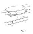
- Figure 4 shows a detail of one patch assembly of the antenna.
- Figure 5 is a plan view of the antenna, looking in the direction of arrow II in Figure 2 but with certain detail omitted for clarity, and
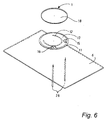
- Figure 6 illustrates, in exploded view, the parts of a simplified antenna, also in accordance with the invention.
- The antenna shown in the drawing is a wide-band low profile dual polarisation antenna capable of receiving and transmitting (either sequentially or simultaneously), orthogonally polarised radio signals. The antenna comprises an array of four
patch assemblies grounded panel 5.Panel 5 andpatch assemblies Panel 5 and the fourpatch assemblies base panel 6 of aluminium. - The patch assemblies 1, 2, 3 and 4 are identical in this case and each comprises a stack of two circular panels. Alternatively, the panels could be either square or a combination of circular and square. The lower
circular panel 11 is held in spaced parallel relationship with respect to thepanel 5 next beneath it by means of an insulating spacer. The lower surface of the lowercircular panel 11 has a parasiticradiating element 12 formed by a copper track deposited on the lower surface of thepanel 11. The upper surface of the lowercircular panel 11 is coated with copper in a circular shape except for two arc-shaped slots slots copper areas slots remaining area 17 of the copper coating. The twoslots areas parasitic element 12 is also symmetrical with respect to this axis, subtending an angle of 135° on each side of the axis. Moreover, theelement 12 is disposed wholly within the volume defined between thecoating area 17 and thepanel 6. In this case, theelement 12 is wholly within the volume defined between thecoating area 17 and thepanel 5, and lies within the plan area or "footprint" of thearea 17. - The upper
circular panel 18 of each patch assembly is held in spaced parallel relationship with respect to the lowercircular panel 11 next beneath it by means of an insulating spacer. The uppercircular panel 18 is made of dielectric material with a circular pattern ofcopper coating 19 on the lower surface of the panel. This upper circular panel could be made of a solid metal, such as aluminium. - It will be appreciated that both the
surface 19 and theoven 17 act as radiating patches. - The upper surface of the
panel 5 is copper coated while the lower surface has a feed/reception network comprising twochannels respective terminal channels panel 5. Each channel divides into fourseparate feed lines small metal pin 24 is used to connect the corresponding feed line, through thepanel 5, to the lower circular panel of a patch assembly. Thepatch assemblies panel 5 are supported on thesupport base panel 6 by means of spacer 25 (Figure 4). - In use as a transmitting antenna, input signals are applied to the
terminals terminal 22 and signals polarised in the orthogonal plane being applied to theterminal 23. The input signals are conducted along thefeed channels feed lines conductive pin 24 conducts the signals from the corresponding feed line to thearea slots area 17 of the copper coating on the upper surface of the lower circular panel. The position (i.e. distance from the edge) and dimension (i.e. arc length) of the twoslots oven 17. - Unwanted cross-couplings created by radiation from within the
patch assemblies parasitic elements 12 formed on the lower surfaces of the lower circular panels. Eachparasitic element 12 acts as a radiating element which radiates energy of the two polarisations into the vicinity of the patch assembly. This radiation, when adjusted properly, can actively cancel the unwanted cross-coupling radiation in the region, which results in high isolation between the polarisations. The position, shape, length and width of each parasitic element are selected for optimal isolation at the frequencies of interest. - Figure 6 illustrates a simplified antenna having only one patch assembly which in structure corresponds to one of the
patch assemblies 1 to 4 of Figures 1 to 4. The antenna of Figure 6 is devoid of thepanel 5 and the feed/reception tracks, signals being conducted to therespective areas pins 26. As before, theareas conductive area 17 on the upper surface of thelower panel 11, the lower surface of which has an arcuateparasitic element 12 subtending an angle of about 270° symmetrically arranged with respect to theareas parasitic element 12 lies wholly within the volume defined between thecoating area 17 and the 6, and within the plan area or "footprint" of thecoating area 17.
Claims (14)
- An antenna for transmission/reception of dual polarised radio signals, the antenna comprising feed/reception means, a radiating patch which is mounted adjacent a panel and which is coupled to the feed/reception means, and a parasitic element, characterised in that the parasitic element is disposed in the volume between the patch and the panel and acts as a radiating element for cancelling unwanted cross-coupling radiation in the vicinity of the patch.
- An antenna according to claim 1 in which the panel comprises a support panel on which the radiating patch is mounted.
- An antenna according to claim 2, in which the support panel or surface thereon acts as a ground plane.
- An antenna according to any of the preceding claims, in which the radiating patch is either one of a first radiating patch situated immediately adjacent the first panel and a second radiating patch which is mounted adjacent the first patch so that the first patch is interposed between the second patch and the panel; the first radiating patch being capacitatively coupled to the feed/reception means, the second patch being electromagnetically coupled to the first patch.
- An antenna according to any of claims 1 to 4, wherein the patch and the parasitic element are defined by metal areas formed on mutually opposite surfaces of a patch panel.
- An antenna according to claim 5 when appended to claim 2, wherein the patch panel is mounted on the support panel in spaced parallel relationship therewith.
- An antenna according to claim 5 or 6, wherein the metal area defining the parasitic element is in the shape of an elongated strip.
- An antenna according to claim 7, wherein the elongated strip is a curved strip.
- An antenna according to claim 8, wherein the parasitic element is a part-circular metal strip, subtending an angle of about 270° symmetrically disposed with relation to the radiating patch.
- An antenna according to any of claims 5 to 10, wherein a metal area defining the patch is capacitively coupled, by uncoated areas, to two metal coated areas aligned along orthogonal axes for handling the orthogonally polarised radio signals, the two metal coated areas forming part of the feed/reception means.
- An antenna according to any of the preceding claims, wherein the radiating patch and the parasitic element form a patch assembly and the antenna has a plurality of such patch assemblies.
- An antenna according to claim 11, wherein the feed/reception means take the form of a feed/reception network having conductive tracks formed by conductive metal areas deposited on the support panel.
- An antenna according to claim 12 and comprising an array of four separated radiating and receiving patch assemblies, which are capable of handling two independent and orthogonally polarised signals simultaneously, there being two input ports for each patch assembly and the ports that correspond to the two polarisations being capacitively coupled to the corresponding tracks of the feed/reception network.
- An antenna according to any of the preceding claims, in which the parasitic element is interposed between the radiating patch and the panel.
Applications Claiming Priority (2)
| Application Number | Priority Date | Filing Date | Title |
|---|---|---|---|
| GB0015693A GB2364175B (en) | 2000-06-28 | 2000-06-28 | Dual polarisation antennas |
| GB0015693 | 2000-06-28 |
Publications (3)
| Publication Number | Publication Date |
|---|---|
| EP1168493A2 true EP1168493A2 (en) | 2002-01-02 |
| EP1168493A3 EP1168493A3 (en) | 2004-01-28 |
| EP1168493B1 EP1168493B1 (en) | 2006-09-06 |
Family
ID=9894477
Family Applications (1)
| Application Number | Title | Priority Date | Filing Date |
|---|---|---|---|
| EP01305415A Expired - Lifetime EP1168493B1 (en) | 2000-06-28 | 2001-06-22 | Dual polarisation antennas |
Country Status (5)
| Country | Link |
|---|---|
| EP (1) | EP1168493B1 (en) |
| AT (1) | ATE339022T1 (en) |
| DE (1) | DE60122830T2 (en) |
| ES (1) | ES2272420T3 (en) |
| GB (1) | GB2364175B (en) |
Cited By (3)
| Publication number | Priority date | Publication date | Assignee | Title |
|---|---|---|---|---|
| US7868843B2 (en) | 2004-08-31 | 2011-01-11 | Fractus, S.A. | Slim multi-band antenna array for cellular base stations |
| US8497814B2 (en) | 2005-10-14 | 2013-07-30 | Fractus, S.A. | Slim triple band antenna array for cellular base stations |
| CN113258272A (en) * | 2020-10-23 | 2021-08-13 | 中兴通讯股份有限公司 | Antenna array and antenna structure |
Families Citing this family (1)
| Publication number | Priority date | Publication date | Assignee | Title |
|---|---|---|---|---|
| CN104600439B (en) * | 2014-12-31 | 2018-03-13 | 广东通宇通讯股份有限公司 | Multifrequency dual polarized antenna |
Citations (4)
| Publication number | Priority date | Publication date | Assignee | Title |
|---|---|---|---|---|
| US4401988A (en) * | 1981-08-28 | 1983-08-30 | The United States Of America As Represented By The Secretary Of The Navy | Coupled multilayer microstrip antenna |
| EP0871238A2 (en) * | 1997-03-25 | 1998-10-14 | Nokia Mobile Phones Ltd. | Broadband antenna realized with shorted microstrips |
| WO1999005754A1 (en) * | 1997-07-23 | 1999-02-04 | Allgon Ab | Antenna device with improved channel isolation |
| US5896107A (en) * | 1997-05-27 | 1999-04-20 | Allen Telecom Inc. | Dual polarized aperture coupled microstrip patch antenna system |
-
2000
- 2000-06-28 GB GB0015693A patent/GB2364175B/en not_active Expired - Fee Related
-
2001
- 2001-06-22 ES ES01305415T patent/ES2272420T3/en not_active Expired - Lifetime
- 2001-06-22 DE DE60122830T patent/DE60122830T2/en not_active Expired - Lifetime
- 2001-06-22 AT AT01305415T patent/ATE339022T1/en not_active IP Right Cessation
- 2001-06-22 EP EP01305415A patent/EP1168493B1/en not_active Expired - Lifetime
Patent Citations (4)
| Publication number | Priority date | Publication date | Assignee | Title |
|---|---|---|---|---|
| US4401988A (en) * | 1981-08-28 | 1983-08-30 | The United States Of America As Represented By The Secretary Of The Navy | Coupled multilayer microstrip antenna |
| EP0871238A2 (en) * | 1997-03-25 | 1998-10-14 | Nokia Mobile Phones Ltd. | Broadband antenna realized with shorted microstrips |
| US5896107A (en) * | 1997-05-27 | 1999-04-20 | Allen Telecom Inc. | Dual polarized aperture coupled microstrip patch antenna system |
| WO1999005754A1 (en) * | 1997-07-23 | 1999-02-04 | Allgon Ab | Antenna device with improved channel isolation |
Non-Patent Citations (1)
| Title |
|---|
| SANAD M: "A COMPACT DUAL-BROADBAND MICROSTRIP ANTENNA HAVING BOTH STACKED AND PLANAR PARASITIC ELEMENTS" IEEE ANTENNAS AND PROPAGATION SOCIETY INTERNATIONAL SYMPOSIUM 1996 DIGEST. BALTIMORE, JULY 21 - 26, 1996. HELD IN CONJUNCTION WITH THE USNC/URSI NATIONAL RADIO SCIENCE MEETING, NEW YORK, IEEE, US, vol. 1, 21 July 1996 (1996-07-21), pages 6-9, XP000782135 ISBN: 0-7803-3217-2 * |
Cited By (7)
| Publication number | Priority date | Publication date | Assignee | Title |
|---|---|---|---|---|
| US7868843B2 (en) | 2004-08-31 | 2011-01-11 | Fractus, S.A. | Slim multi-band antenna array for cellular base stations |
| US8497814B2 (en) | 2005-10-14 | 2013-07-30 | Fractus, S.A. | Slim triple band antenna array for cellular base stations |
| US8754824B2 (en) | 2005-10-14 | 2014-06-17 | Fractus, S.A. | Slim triple band antenna array for cellular base stations |
| US9450305B2 (en) | 2005-10-14 | 2016-09-20 | Fractus, S.A. | Slim triple band antenna array for cellular base stations |
| US10211519B2 (en) | 2005-10-14 | 2019-02-19 | Fractus, S.A. | Slim triple band antenna array for cellular base stations |
| US10910699B2 (en) | 2005-10-14 | 2021-02-02 | Commscope Technologies Llc | Slim triple band antenna array for cellular base stations |
| CN113258272A (en) * | 2020-10-23 | 2021-08-13 | 中兴通讯股份有限公司 | Antenna array and antenna structure |
Also Published As
| Publication number | Publication date |
|---|---|
| EP1168493A3 (en) | 2004-01-28 |
| DE60122830D1 (en) | 2006-10-19 |
| EP1168493B1 (en) | 2006-09-06 |
| GB2364175B (en) | 2004-05-05 |
| GB0015693D0 (en) | 2000-08-16 |
| ES2272420T3 (en) | 2007-05-01 |
| GB2364175A (en) | 2002-01-16 |
| DE60122830T2 (en) | 2007-04-05 |
| ATE339022T1 (en) | 2006-09-15 |
Similar Documents
| Publication | Publication Date | Title |
|---|---|---|
| US11276931B2 (en) | Antenna device and antenna array | |
| US5771025A (en) | Folded mono-bow antennas and antenna systems for use in cellular and other wireless communication systems | |
| US6366258B2 (en) | Low profile high polarization purity dual-polarized antennas | |
| US6664932B2 (en) | Multifunction antenna for wireless and telematic applications | |
| US7196674B2 (en) | Dual polarized three-sector base station antenna with variable beam tilt | |
| AU724045B2 (en) | Antenna mutual coupling neutralizer | |
| US8130164B2 (en) | Broadband coplanar antenna element | |
| US20020075194A1 (en) | Mechanically steerable array antenna | |
| CN108336490B (en) | High-isolation broadband MIMO antenna | |
| CN1212482A (en) | High isolation dual polarized antenna system with microstrip-fed aperture coupled patches | |
| CN101223672A (en) | Antenna system with second-order diversity and card for wireless communication apparatus which is equipped with one such device | |
| WO2001013461A1 (en) | Diversity antenna system for lan communication system | |
| WO1998000882A1 (en) | Folded mono-bow antennas and antenna systems for use in cellular and other wireless communications systems | |
| EP3465823B1 (en) | C-fed antenna formed on multi-layer printed circuit board edge | |
| US20100201593A1 (en) | Antenna arrangement for a multi radiator base station antenna | |
| US20200091990A1 (en) | Multi-band antenna arrangements | |
| WO2017107501A1 (en) | A low coupling 2×2 mimo array | |
| EP1022803B1 (en) | Dual polarisation antennas | |
| Kim et al. | High isolation internal dual-band planar inverted-F antenna diversity system with band-notched slots for MIMO terminals | |
| EP2005522B1 (en) | Broadband dual polarized base station antenna | |
| EP4290688A1 (en) | Antenna assemblies and antenna modules for use in wireless communication systems | |
| EP1168493B1 (en) | Dual polarisation antennas | |
| JP2007124346A (en) | Antenna element and array type antenna | |
| WO1998027614A1 (en) | Antenna with diversity transformation | |
| EP3916913A1 (en) | Calibration device, base station antenna and a communication assembly |
Legal Events
| Date | Code | Title | Description |
|---|---|---|---|
| PUAI | Public reference made under article 153(3) epc to a published international application that has entered the european phase |
Free format text: ORIGINAL CODE: 0009012 |
|
| AK | Designated contracting states |
Kind code of ref document: A2 Designated state(s): AT BE CH CY DE DK ES FI FR GB GR IE IT LI LU MC NL PT SE TR |
|
| AX | Request for extension of the european patent |
Free format text: AL;LT;LV;MK;RO;SI |
|
| PUAL | Search report despatched |
Free format text: ORIGINAL CODE: 0009013 |
|
| AK | Designated contracting states |
Kind code of ref document: A3 Designated state(s): AT BE CH CY DE DK ES FI FR GB GR IE IT LI LU MC NL PT SE TR |
|
| AX | Request for extension of the european patent |
Extension state: AL LT LV MK RO SI |
|
| RIC1 | Information provided on ipc code assigned before grant |
Ipc: 7H 01Q 9/04 B Ipc: 7H 01Q 21/08 B Ipc: 7H 01Q 21/24 A |
|
| 17P | Request for examination filed |
Effective date: 20040728 |
|
| AKX | Designation fees paid |
Designated state(s): AT BE CH CY DE DK ES FI FR GB GR IE IT LI LU MC NL PT SE TR |
|
| 17Q | First examination report despatched |
Effective date: 20041007 |
|
| GRAP | Despatch of communication of intention to grant a patent |
Free format text: ORIGINAL CODE: EPIDOSNIGR1 |
|
| GRAS | Grant fee paid |
Free format text: ORIGINAL CODE: EPIDOSNIGR3 |
|
| GRAA | (expected) grant |
Free format text: ORIGINAL CODE: 0009210 |
|
| AK | Designated contracting states |
Kind code of ref document: B1 Designated state(s): AT BE CH CY DE DK ES FI FR GB GR IE IT LI LU MC NL PT SE TR |
|
| PG25 | Lapsed in a contracting state [announced via postgrant information from national office to epo] |
Ref country code: IT Free format text: LAPSE BECAUSE OF FAILURE TO SUBMIT A TRANSLATION OF THE DESCRIPTION OR TO PAY THE FEE WITHIN THE PRESCRIBED TIME-LIMIT;WARNING: LAPSES OF ITALIAN PATENTS WITH EFFECTIVE DATE BEFORE 2007 MAY HAVE OCCURRED AT ANY TIME BEFORE 2007. THE CORRECT EFFECTIVE DATE MAY BE DIFFERENT FROM THE ONE RECORDED. Effective date: 20060906 Ref country code: BE Free format text: LAPSE BECAUSE OF FAILURE TO SUBMIT A TRANSLATION OF THE DESCRIPTION OR TO PAY THE FEE WITHIN THE PRESCRIBED TIME-LIMIT Effective date: 20060906 Ref country code: FI Free format text: LAPSE BECAUSE OF FAILURE TO SUBMIT A TRANSLATION OF THE DESCRIPTION OR TO PAY THE FEE WITHIN THE PRESCRIBED TIME-LIMIT Effective date: 20060906 Ref country code: AT Free format text: LAPSE BECAUSE OF FAILURE TO SUBMIT A TRANSLATION OF THE DESCRIPTION OR TO PAY THE FEE WITHIN THE PRESCRIBED TIME-LIMIT Effective date: 20060906 Ref country code: CH Free format text: LAPSE BECAUSE OF FAILURE TO SUBMIT A TRANSLATION OF THE DESCRIPTION OR TO PAY THE FEE WITHIN THE PRESCRIBED TIME-LIMIT Effective date: 20060906 Ref country code: LI Free format text: LAPSE BECAUSE OF FAILURE TO SUBMIT A TRANSLATION OF THE DESCRIPTION OR TO PAY THE FEE WITHIN THE PRESCRIBED TIME-LIMIT Effective date: 20060906 Ref country code: NL Free format text: LAPSE BECAUSE OF FAILURE TO SUBMIT A TRANSLATION OF THE DESCRIPTION OR TO PAY THE FEE WITHIN THE PRESCRIBED TIME-LIMIT Effective date: 20060906 |
|
| REG | Reference to a national code |
Ref country code: GB Ref legal event code: FG4D |
|
| REG | Reference to a national code |
Ref country code: CH Ref legal event code: EP |
|
| REG | Reference to a national code |
Ref country code: IE Ref legal event code: FG4D |
|
| REF | Corresponds to: |
Ref document number: 60122830 Country of ref document: DE Date of ref document: 20061019 Kind code of ref document: P |
|
| PG25 | Lapsed in a contracting state [announced via postgrant information from national office to epo] |
Ref country code: DK Free format text: LAPSE BECAUSE OF FAILURE TO SUBMIT A TRANSLATION OF THE DESCRIPTION OR TO PAY THE FEE WITHIN THE PRESCRIBED TIME-LIMIT Effective date: 20061206 Ref country code: SE Free format text: LAPSE BECAUSE OF FAILURE TO SUBMIT A TRANSLATION OF THE DESCRIPTION OR TO PAY THE FEE WITHIN THE PRESCRIBED TIME-LIMIT Effective date: 20061206 |
|
| PG25 | Lapsed in a contracting state [announced via postgrant information from national office to epo] |
Ref country code: PT Free format text: LAPSE BECAUSE OF FAILURE TO SUBMIT A TRANSLATION OF THE DESCRIPTION OR TO PAY THE FEE WITHIN THE PRESCRIBED TIME-LIMIT Effective date: 20070219 |
|
| NLV1 | Nl: lapsed or annulled due to failure to fulfill the requirements of art. 29p and 29m of the patents act | ||
| ET | Fr: translation filed | ||
| REG | Reference to a national code |
Ref country code: CH Ref legal event code: PL |
|
| REG | Reference to a national code |
Ref country code: ES Ref legal event code: FG2A Ref document number: 2272420 Country of ref document: ES Kind code of ref document: T3 |
|
| PLBE | No opposition filed within time limit |
Free format text: ORIGINAL CODE: 0009261 |
|
| STAA | Information on the status of an ep patent application or granted ep patent |
Free format text: STATUS: NO OPPOSITION FILED WITHIN TIME LIMIT |
|
| 26N | No opposition filed |
Effective date: 20070607 |
|
| REG | Reference to a national code |
Ref country code: GB Ref legal event code: 732E |
|
| PG25 | Lapsed in a contracting state [announced via postgrant information from national office to epo] |
Ref country code: MC Free format text: LAPSE BECAUSE OF NON-PAYMENT OF DUE FEES Effective date: 20070630 |
|
| REG | Reference to a national code |
Ref country code: FR Ref legal event code: TP |
|
| PG25 | Lapsed in a contracting state [announced via postgrant information from national office to epo] |
Ref country code: GR Free format text: LAPSE BECAUSE OF FAILURE TO SUBMIT A TRANSLATION OF THE DESCRIPTION OR TO PAY THE FEE WITHIN THE PRESCRIBED TIME-LIMIT Effective date: 20061207 |
|
| REG | Reference to a national code |
Ref country code: FR Ref legal event code: TP |
|
| REG | Reference to a national code |
Ref country code: GB Ref legal event code: 732E Free format text: REGISTERED BETWEEN 20090319 AND 20090325 |
|
| PG25 | Lapsed in a contracting state [announced via postgrant information from national office to epo] |
Ref country code: LU Free format text: LAPSE BECAUSE OF NON-PAYMENT OF DUE FEES Effective date: 20070622 Ref country code: CY Free format text: LAPSE BECAUSE OF FAILURE TO SUBMIT A TRANSLATION OF THE DESCRIPTION OR TO PAY THE FEE WITHIN THE PRESCRIBED TIME-LIMIT Effective date: 20060906 |
|
| REG | Reference to a national code |
Ref country code: FR Ref legal event code: TP |
|
| PG25 | Lapsed in a contracting state [announced via postgrant information from national office to epo] |
Ref country code: TR Free format text: LAPSE BECAUSE OF FAILURE TO SUBMIT A TRANSLATION OF THE DESCRIPTION OR TO PAY THE FEE WITHIN THE PRESCRIBED TIME-LIMIT Effective date: 20060906 |
|
| PGFP | Annual fee paid to national office [announced via postgrant information from national office to epo] |
Ref country code: ES Payment date: 20121214 Year of fee payment: 12 |
|
| PGFP | Annual fee paid to national office [announced via postgrant information from national office to epo] |
Ref country code: DE Payment date: 20130625 Year of fee payment: 13 |
|
| PGFP | Annual fee paid to national office [announced via postgrant information from national office to epo] |
Ref country code: IT Payment date: 20130626 Year of fee payment: 13 |
|
| PGFP | Annual fee paid to national office [announced via postgrant information from national office to epo] |
Ref country code: FR Payment date: 20130716 Year of fee payment: 13 |
|
| REG | Reference to a national code |
Ref country code: DE Ref legal event code: R119 Ref document number: 60122830 Country of ref document: DE |
|
| PGFP | Annual fee paid to national office [announced via postgrant information from national office to epo] |
Ref country code: IE Payment date: 20141221 Year of fee payment: 14 Ref country code: GB Payment date: 20141124 Year of fee payment: 14 |
|
| REG | Reference to a national code |
Ref country code: DE Ref legal event code: R119 Ref document number: 60122830 Country of ref document: DE Effective date: 20150101 |
|
| REG | Reference to a national code |
Ref country code: FR Ref legal event code: ST Effective date: 20150227 |
|
| PG25 | Lapsed in a contracting state [announced via postgrant information from national office to epo] |
Ref country code: DE Free format text: LAPSE BECAUSE OF NON-PAYMENT OF DUE FEES Effective date: 20150101 Ref country code: IT Free format text: LAPSE BECAUSE OF NON-PAYMENT OF DUE FEES Effective date: 20140622 |
|
| PG25 | Lapsed in a contracting state [announced via postgrant information from national office to epo] |
Ref country code: FR Free format text: LAPSE BECAUSE OF NON-PAYMENT OF DUE FEES Effective date: 20140630 |
|
| REG | Reference to a national code |
Ref country code: ES Ref legal event code: FD2A Effective date: 20150728 |
|
| PG25 | Lapsed in a contracting state [announced via postgrant information from national office to epo] |
Ref country code: ES Free format text: LAPSE BECAUSE OF NON-PAYMENT OF DUE FEES Effective date: 20140623 |
|
| GBPC | Gb: european patent ceased through non-payment of renewal fee |
Effective date: 20150622 |
|
| REG | Reference to a national code |
Ref country code: IE Ref legal event code: MM4A |
|
| PG25 | Lapsed in a contracting state [announced via postgrant information from national office to epo] |
Ref country code: IE Free format text: LAPSE BECAUSE OF NON-PAYMENT OF DUE FEES Effective date: 20150622 Ref country code: GB Free format text: LAPSE BECAUSE OF NON-PAYMENT OF DUE FEES Effective date: 20150622 |