EP1198821B1 - Plasma etching chamber - Google Patents
Plasma etching chamber Download PDFInfo
- Publication number
- EP1198821B1 EP1198821B1 EP00945097A EP00945097A EP1198821B1 EP 1198821 B1 EP1198821 B1 EP 1198821B1 EP 00945097 A EP00945097 A EP 00945097A EP 00945097 A EP00945097 A EP 00945097A EP 1198821 B1 EP1198821 B1 EP 1198821B1
- Authority
- EP
- European Patent Office
- Prior art keywords
- wafer
- edge ring
- chuck
- plasma processing
- coupled
- Prior art date
- Legal status (The legal status is an assumption and is not a legal conclusion. Google has not performed a legal analysis and makes no representation as to the accuracy of the status listed.)
- Expired - Lifetime
Links
Images


Classifications
-
- H—ELECTRICITY
- H01—ELECTRIC ELEMENTS
- H01L—SEMICONDUCTOR DEVICES NOT COVERED BY CLASS H10
- H01L21/00—Processes or apparatus adapted for the manufacture or treatment of semiconductor or solid state devices or of parts thereof
- H01L21/02—Manufacture or treatment of semiconductor devices or of parts thereof
- H01L21/04—Manufacture or treatment of semiconductor devices or of parts thereof the devices having at least one potential-jump barrier or surface barrier, e.g. PN junction, depletion layer or carrier concentration layer
- H01L21/18—Manufacture or treatment of semiconductor devices or of parts thereof the devices having at least one potential-jump barrier or surface barrier, e.g. PN junction, depletion layer or carrier concentration layer the devices having semiconductor bodies comprising elements of Group IV of the Periodic System or AIIIBV compounds with or without impurities, e.g. doping materials
- H01L21/30—Treatment of semiconductor bodies using processes or apparatus not provided for in groups H01L21/20 - H01L21/26
- H01L21/302—Treatment of semiconductor bodies using processes or apparatus not provided for in groups H01L21/20 - H01L21/26 to change their surface-physical characteristics or shape, e.g. etching, polishing, cutting
- H01L21/306—Chemical or electrical treatment, e.g. electrolytic etching
- H01L21/3065—Plasma etching; Reactive-ion etching
-
- H—ELECTRICITY
- H01—ELECTRIC ELEMENTS
- H01L—SEMICONDUCTOR DEVICES NOT COVERED BY CLASS H10
- H01L21/00—Processes or apparatus adapted for the manufacture or treatment of semiconductor or solid state devices or of parts thereof
- H01L21/67—Apparatus specially adapted for handling semiconductor or electric solid state devices during manufacture or treatment thereof; Apparatus specially adapted for handling wafers during manufacture or treatment of semiconductor or electric solid state devices or components ; Apparatus not specifically provided for elsewhere
- H01L21/67005—Apparatus not specifically provided for elsewhere
- H01L21/67011—Apparatus for manufacture or treatment
- H01L21/67017—Apparatus for fluid treatment
- H01L21/67063—Apparatus for fluid treatment for etching
- H01L21/67069—Apparatus for fluid treatment for etching for drying etching
-
- H—ELECTRICITY
- H01—ELECTRIC ELEMENTS
- H01J—ELECTRIC DISCHARGE TUBES OR DISCHARGE LAMPS
- H01J37/00—Discharge tubes with provision for introducing objects or material to be exposed to the discharge, e.g. for the purpose of examination or processing thereof
- H01J37/32—Gas-filled discharge tubes
- H01J37/32431—Constructional details of the reactor
- H01J37/32623—Mechanical discharge control means
- H01J37/32642—Focus rings
-
- H—ELECTRICITY
- H01—ELECTRIC ELEMENTS
- H01L—SEMICONDUCTOR DEVICES NOT COVERED BY CLASS H10
- H01L21/00—Processes or apparatus adapted for the manufacture or treatment of semiconductor or solid state devices or of parts thereof
- H01L21/67—Apparatus specially adapted for handling semiconductor or electric solid state devices during manufacture or treatment thereof; Apparatus specially adapted for handling wafers during manufacture or treatment of semiconductor or electric solid state devices or components ; Apparatus not specifically provided for elsewhere
- H01L21/683—Apparatus specially adapted for handling semiconductor or electric solid state devices during manufacture or treatment thereof; Apparatus specially adapted for handling wafers during manufacture or treatment of semiconductor or electric solid state devices or components ; Apparatus not specifically provided for elsewhere for supporting or gripping
- H01L21/687—Apparatus specially adapted for handling semiconductor or electric solid state devices during manufacture or treatment thereof; Apparatus specially adapted for handling wafers during manufacture or treatment of semiconductor or electric solid state devices or components ; Apparatus not specifically provided for elsewhere for supporting or gripping using mechanical means, e.g. chucks, clamps or pinches
- H01L21/68714—Apparatus specially adapted for handling semiconductor or electric solid state devices during manufacture or treatment thereof; Apparatus specially adapted for handling wafers during manufacture or treatment of semiconductor or electric solid state devices or components ; Apparatus not specifically provided for elsewhere for supporting or gripping using mechanical means, e.g. chucks, clamps or pinches the wafers being placed on a susceptor, stage or support
- H01L21/68721—Apparatus specially adapted for handling semiconductor or electric solid state devices during manufacture or treatment thereof; Apparatus specially adapted for handling wafers during manufacture or treatment of semiconductor or electric solid state devices or components ; Apparatus not specifically provided for elsewhere for supporting or gripping using mechanical means, e.g. chucks, clamps or pinches the wafers being placed on a susceptor, stage or support characterised by edge clamping, e.g. clamping ring
-
- H—ELECTRICITY
- H01—ELECTRIC ELEMENTS
- H01L—SEMICONDUCTOR DEVICES NOT COVERED BY CLASS H10
- H01L21/00—Processes or apparatus adapted for the manufacture or treatment of semiconductor or solid state devices or of parts thereof
- H01L21/67—Apparatus specially adapted for handling semiconductor or electric solid state devices during manufacture or treatment thereof; Apparatus specially adapted for handling wafers during manufacture or treatment of semiconductor or electric solid state devices or components ; Apparatus not specifically provided for elsewhere
- H01L21/683—Apparatus specially adapted for handling semiconductor or electric solid state devices during manufacture or treatment thereof; Apparatus specially adapted for handling wafers during manufacture or treatment of semiconductor or electric solid state devices or components ; Apparatus not specifically provided for elsewhere for supporting or gripping
- H01L21/687—Apparatus specially adapted for handling semiconductor or electric solid state devices during manufacture or treatment thereof; Apparatus specially adapted for handling wafers during manufacture or treatment of semiconductor or electric solid state devices or components ; Apparatus not specifically provided for elsewhere for supporting or gripping using mechanical means, e.g. chucks, clamps or pinches
- H01L21/68714—Apparatus specially adapted for handling semiconductor or electric solid state devices during manufacture or treatment thereof; Apparatus specially adapted for handling wafers during manufacture or treatment of semiconductor or electric solid state devices or components ; Apparatus not specifically provided for elsewhere for supporting or gripping using mechanical means, e.g. chucks, clamps or pinches the wafers being placed on a susceptor, stage or support
- H01L21/68735—Apparatus specially adapted for handling semiconductor or electric solid state devices during manufacture or treatment thereof; Apparatus specially adapted for handling wafers during manufacture or treatment of semiconductor or electric solid state devices or components ; Apparatus not specifically provided for elsewhere for supporting or gripping using mechanical means, e.g. chucks, clamps or pinches the wafers being placed on a susceptor, stage or support characterised by edge profile or support profile
-
- Y—GENERAL TAGGING OF NEW TECHNOLOGICAL DEVELOPMENTS; GENERAL TAGGING OF CROSS-SECTIONAL TECHNOLOGIES SPANNING OVER SEVERAL SECTIONS OF THE IPC; TECHNICAL SUBJECTS COVERED BY FORMER USPC CROSS-REFERENCE ART COLLECTIONS [XRACs] AND DIGESTS
- Y10—TECHNICAL SUBJECTS COVERED BY FORMER USPC
- Y10S—TECHNICAL SUBJECTS COVERED BY FORMER USPC CROSS-REFERENCE ART COLLECTIONS [XRACs] AND DIGESTS
- Y10S156/00—Adhesive bonding and miscellaneous chemical manufacture
- Y10S156/915—Differential etching apparatus including focus ring surrounding a wafer for plasma apparatus
Description
- The present invention relates to a plasma processing chamber for etching a substrate.
- In the fabrication of semiconductor-based devices, e.g., integrated circuits or flat panel displays, layers of materials may alternately be deposited onto and etched from a substrate surface. As is well known in the art, the etching of the deposited layers may be accomplished by a variety of techniques, including plasma-enhanced etching. In plasma-enhanced etching, the actual etching typically takes place inside a plasma processing chamber of a plasma processing system. To form the desired pattern on the substrate surface, an appropriate mask (e.g., a photoresist mask) is typically provided. A plasma is then formed from a suitable etchant source gas, or mixture of gases, and used to etch areas that are unprotected by the mask, thereby leaving behind the desired pattern.
- To facilitate discussion.
FIG. 1A depicts a simplifiedplasma processing apparatus 100 suitable for fabrication of semiconductor-based devices. The simplifiedplasma processing apparatus 100 includes awafer processing chamber 102 having an electrostatic chuck (ESC) 104. Thechuck 104 acts as an electrode and supports a wafer 106 (i.e., substrate) during fabrication. Anedge ring 108 borders the edge of thechuck 104. In the case of etch processes, a number of parameters within thewafer processing chamber 102 are tightly controlled to maintain high tolerance etch results. Process parameters governing etch results may include gas composition, plasma excitation, plasma distribution over thewafer 106, etc. Since the etch tolerance (and resulting semiconductor-based device performance) is highly sensitive to such process parameters, accurate control thereof is required. - The surface of the
wafer 106 is etched by an appropriate etchant source gas that is released into thewafer processing chamber 102. The etchant source gas can be released through a showerhead. The etchant source gas may also be released by other mechanisms such as via a gas ring disposed inside the chamber or via ports built into the walls of thewafer processing chamber 102. During ion-assisted etch processes, Radio Frequency (RF) power supplied to showerhead ignites the etchant source gas, thereby forming a plasma cloud ("plasma") abovewafer 106 during etch processes. It should be noted that other means of plasma excitation may also be used. For example, the application of microwave energy, the use of inductive coils, the introduction of a wave excited by an antenna, or capacitive coupling to the showerhead can also be used to excite the plasma. In ion-assisted etch processes,chuck 104 is typically RF powered using a RF power supply (not shown). - In an ion-assisted etch process, the local etch rate is dominated by ion concentration. Ion-assisted etch processes are typically used to perform oxide etches or polysilicon etches. In other words, ion driven/assisted etch processes generally refer to etching processes wherein the etching is predominately facilitated by the physical reaction of the accelerated plasma ions ("ions") with the wafer (substrate). Ion-assisted etching applications include, for example, sputtering, Reactive Ion Etching (RIE), chemical sputtering, chemically assisted physical sputtering, and physically assisted chemical sputtering.
- With ion-assisted etching, application of RF power to the chuck 104 (as well as the showerhead) results in the formation of an electric field and in turn a
sheath 112 above thewafer 106. The electric field associated with thesheath 112 promotes the acceleration of ions toward the top surface of thewafer 106. Ideally, the accelerated ions collide at an angle that is substantially perpendicular (i.e., substantially normal or about 90 degrees) with the respect to the surface of thewafer 106 during etch processes. The accelerated ions that collide with thewafer 106 operate to "physically" etch thewafer 106. - The
edge ring 108 is an insulator material that is electrically floating (i.e., not RF powered).Edge ring 108 is used to shield the edge of thechuck 104 from ion bombardment such as during etch processes. Edgering 108 can also help focus the ion bombardment with respect to thewafer 106. As shown inFigure 1A , thechuck 104 can be surrounded by aninner surface 114 of theedge ring 108. Theinner surface 114 is also within the outer edge of thewafer 106. - An
outer surface 116 of theedge ring 108 extends beyond the outer edge of thewafer 106. An upper portion of theinner surface 114 of theedge ring 114 is adjacent to not only thechuck 104 but also thewafer 106. Conventionally, atop surface 118 of theedge ring 108 is below or about the same level as a top surface of thewafer 106. - One major problem associated with ion-assisted etch processes using a convention plasma processing apparatus is that the etch rate is not uniform across the
wafer 106. More specifically, etch rate at locations near the edges of the wafer is significantly higher than the etch rate for points near the center of the wafer.FIG. 1B illustrates a cross-section of thewafer 106 following etch processes where the etched depth is greater at a perimeter portion 120 of thewafer 106 than at a middle portion 122 of thewafer 106. - The non-uniform etch rate is attributed primarily to the non-uniform thickness of the
sheath 112 above the surface ofwafer 106. As depicted inFIG. 1A , the thickness (or the plasma density at the sheath boundary) of thesheath 112 at the middle portion 120 of thewafer 106 is significantly thicker than the thickness (density) of thesheath 112 at theperimeter portion 116 of thewafer 106. That is, in the vicinity of the electronically floating region above theedge ring 108 the sheath "curves" near the perimeter of thewafer 106. The sheath curvature around the perimeter of thewafer 106 causes relatively more ions to collide near the perimeter of thewafer 106 during ion-assisted etch processes. A higher collision rate near the perimeter results in relatively higher etch rates near the perimeter of the wafer (seeFIG. 1B ). - An additional problem is caused by the sheath curvature. In particular, the sheath curvature near the perimeter of the
wafer 106 induces the ions to collide at angles that are not substantially perpendicular (i.e., not substantially normal or about 90 degrees) with respect to the surface of thewafer 106. In ion-assisted etch processes, ion collisions at such non-perpendicular angles also contribute to higher etch rates. Furthermore, the non-perpendicular angles of ion collision near the edges can have an undesired "tilting" effect on the etched features (e.g., trenches, vias or lines) on thewafer 106. Tilting generally refers to an undesired effect during etching whereby one or more sides of a feature are not substantially perpendicular with the surface of a wafer. Here, at the perimeter of thewafer 106, the "tilting" effect produces an asymmetric feature. Features are intended to be symmetric, so asymmetric features are undesired and can cause severe problems that render a fabricated integrated circuit essentially defective. - One potential solution to address some of the problems associated with non-uniformity of etch rates in ion-assisted etching processes is to enlarge the chuck so that it extends beyond the edges of wafer. Enlarging the chuck would effectively shift the sheath curvature beyond the edges of the wafer. This may be a feasible solution for purely chemical etching application. However, this solution would not be feasible for ion-assisted etch processes since the extended portion of the chuck would also be exposed to ions and the etching process. Exposing the chuck can cause particulate and/or heavy metal contamination during the ion-assisted etch processes. The extended portions of the chuck would also be exposed to significantly higher etch rates to compound the problems associated with contamination. Further, the high etch rates at the exposed portions of the chuck can rapidly deteriorate the chuck which can lead to often replacement of the entire chuck which is an expensive part to be a consumable.
- To curtail some of the problems associated with etch rate non-uniformity associated with ion-assisted etch processes, it may be possible to alter the distribution of plasma above the wafer. For example, a conventional "focus ring" can be placed above the sheath. By attempting to focus the plasma on the wafer, it is believed that a traditional focus ring may reduce the ion density (plasma) distributed over the edges of a wafer. If successful, the reduction of plasma distribution could result in lowering the etch rates near the perimeter of the wafer (i.e. the number of ions that collide near the edges would be reduced). Using an external element such as a focus ring may marginally compensate for the sheath curvature effect. However, introduction of an another element to the ionized etching process can raise new problems associated with contamination and/or costly consumable parts. In addition, use of a traditional focus ring may not even be feasible for some ionized etching applications.
- In view of the foregoing, there is a need for improved methods and apparatus for improving etch rate uniformity in ion-assisted processes.
-
WO99/1478 -
EP-A-066049 - Broadly speaking, the invention relates to a plasma processing chamber for ion-assisted etch processing. The invention operates to improve etch rate uniformity across a substrate (wafer).
- According to the present invention, there is provided a plasma processing chamber according to claim 1.
- The invention has numerous advantages. One advantage of the invention is that etch rate uniformity across a substrate surface is significantly improved. Another advantage of the invention is that significant improvement in etch rate uniformity is achieved without risking contamination of the processing chamber. Yet another advantage is that tilting of etched features can be substantially eliminated.
- Other aspects and advantages of the invention will become apparent from the following detailed description, taken in conjunction with the accompanying drawings, illustrating by way of example the principles of the invention.
- The present invention will be readily understood by the following detailed description in conjunction with the accompanying drawings, wherein like reference numerals designate like structural elements, and in which:
-
Fig. 1A depicts a simplifiedplasma processing apparatus 100 suitable for fabrication of semiconductor-based devices. -
FIG. 1B illustrates a cross-section of a wafer following etch processes where the etched depth is greater at a perimeter portion of the wafer than at a middle portion of the wafer. -
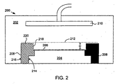
FIG. 2 illustrates a plasma processing apparatus including an elevated edge ring. -
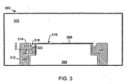
FIG. 3 illustrates aplasma processing apparatus 300 including a grooved edge ring. -
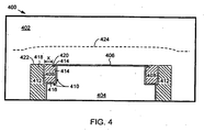
FIG. 4 illustrates aplasma processing apparatus 400 including an inner RF coupled edge ring and an outer edge ring. -
FIG. 5 illustrates aplasma processing apparatus 500 including a RF coupler, an inner RF coupled edge ring and an outer edge ring, in accordance to an embodiment of the invention. -
FIG. 6 illustrates a portion of a cross section of aplasma processing apparatus 600 including dielectric fillers. - The invention pertains to a plasma processing chamber for ion-assisted etch processing. The invention operates to improve etch rate uniformity across a substrate (wafer). Etch rate uniformity improvement provided by the invention not only improves fabrication yields but also is cost efficient and does not risk particulate and/or heavy metal contamination.
- An embodiments of the invention is discussed below with reference to
FIG. 5 . However, those skilled in the art will readily appreciate that the detailed description given herein with respect to this figure is for explanatory purposes as the invention is defined by the claims. -
FIG. 2 illustrates aplasma processing apparatus 200. Theplasma processing apparatus 200 includes awafer processing chamber 202 having an electrostatic chuck (ESC) 204. Thechuck 204 acts as an electrode and supports a wafer 206 (i.e.. substrate) during fabrication. Anelevated edge ring 208 borders the edge of thechuck 204 and extends upward beyond the top surface of thewafer 206. - The
elevated edge ring 208 is typically an insulator material that is electrically floating (i.e., not RF powered).Elevated edge ring 208 is used to shield the edge of thechuck 204 from ion bombardment such as during etch processes. As shown inFIG. 2 . thechuck 204 is surrounded by aninner surface 214 of theedge ring 208. Theinner surface 214 is also within the outer edge of thewafer 206. - An
outer surface 216 of theedge ring 208 extends beyond the outer edge of thewafer 206. An upper portion of theinner surface 214 of theelevated edge ring 208 includes a recessedarea 218. Thewafer 206 sits in the recessedarea 218 and covers a portion of the upper portion of theinner surface 114. Atop surface 220 of theelevated edge ring 208 is above a top surface of thewafer 206 by a predetermined distance D. The predetermined distance D varies depending on implementation and particular processes being performed. Typically, the predetermined distance D is on the order of 1 to 10 millimeters. In the case of etch processes, a number of parameters within thewafer processing chamber 202 are tightly controlled to maintain high tolerance etch results. Process parameters governing etch results may include gas composition, plasma excitation, plasma distribution over thewafer 206, etc. Since the etch tolerance (and resulting semiconductor-based device performance) is highly sensitive to such process parameters, accurate control thereof is required. - The surface of the
wafer 206 is etched by an appropriate etchant source gas that released into thewafer processing chamber 202. The etchant source gas can be released through a showerhead 210. The etchant source gas may also be released by other mechanisms such as via a gas ring disposed inside thewafer processing chamber 202 or via ports built into the walls of thewafer processing chamber 202. During ion-assisted etch processes, Radio Frequency (RF) power supplied to showerhead 210 ignites the etchant source gas, thereby forming a plasma cloud ("plasma") abovewafer 206 during etch processes. In ion-assisted etch processes, chuck 204 is typically RF powered using a RF power supply (not shown). - In an ion-assisted etch process, the local etch rate is dominated by ion concentration. Ion-assisted etch processes are typically used to perform oxide etches or polysilicon etches. In other words, ion driven/assisted etch processes generally refer to etching processes wherein the etching is predominately facilitated by the physical reaction of the accelerated plasma ions ("ions") with the wafer (substrate). Ion-assisted etching applications include, for example, sputtering. Reactive Ion Etching (RIE), chemical sputtering, chemically assisted physical sputtering and physically assisted chemical sputtering.
- With ion-assisted etching, application of RF power to the chuck 204 (as well as the showerhead 210) results in the formation of an electric field and in turn a
sheath 212 above thewafer 206. The electric field associated with thesheath 212 promotes the acceleration of ions toward the top surface of thewafer 206. Theelevated edge ring 208 extends upward beyond the top surface of thewafer 206 as previous noted. By extending above the top surface of thewafer 206, theelevated edge ring 208 performs a corrective action on thesheath 212. Specifically, in one embodiment, the thickness (or density) of thesheath 212 near the perimeter of thewafer 206 becomes substantially the same thickness (density) as the middle portion of thewafer 206. Note that the resultingsheath 212 can be made essentially uniform across thewafer 206 using theelevated edge ring 208. Hence, in comparison to thesheath 112 ofFIG. 1A , thesheath 212 is significantly improved. As a result, of the uniform thickness (density) of thesheath 212, the collision rate of ions with the surface of thewafer 206 is substantially more uniform across the entire surface of thewafer 206 than obtained by conventional approaches. Furthermore, the angle at which the ions collide with the surface of thewafer 206 is substantially normal not only at inner regions but also peripheral regions of thewafer 206. Consequently, the etch rate across the entire surface of thewafer 206 is substantially more uniform than conventionally achieved and etched features at the peripheral regions do not suffer from "tilting" problems. -
FIG. 3 illustrates aplasma processing apparatus 300. - The
plasma processing apparatus 300 includes awafer processing chamber 302 having an electrostatic chuck (ESC) 304. Thechuck 304 acts as an electrode and supports a wafer 306 (i.e. substrate) during fabrication. Agrooved edge ring 308 borders the edge of thechuck 304. - The
grooved edge ring 308 is typically an insulator material that is electrically floating (i.e. not RF powered).Grooved edge ring 308 is used to shield the edge of thechuck 304 from ion bombardment such as during etching processes. As shown inFIG. 3 , thechuck 304 is surrounded by aninner surface 310 of theedge ring 308. Theinner surface 310 is also within the outer edge of the wafer 306. Anouter surface 312 of thegrooved edge ring 308 extends beyond the outer edge of the wafer 306. In one embodiment, anupper surface 314 of thegrooved edge ring 308 is substantially about the same level as anupper surface 316 of the wafer 306. However, an upper surface of thegrooved edge ring 308 adjacent the edge of the wafer 306 has a groovedarea 318. As shown inFIG. 3 , thegrooved area 318 is defined by a firstsloping portion 320, a secondsloping portion 322, and abottom notch 324 connecting the first and secondsloping portions sloping surface 320 connects theupper surface 314 to the partially coveredarea 322. - As discussed earlier, application of RF power to the chuck 306 results in the formation of an electric field and in turn a sheath above the wafer 306. The electric field associated with the sheath promotes the acceleration of ions towards the top surface of the wafer 306. The
grooved edge ring 308 provides thegrooved area 318 that is essentially under the edge of the wafer 306. As illustrated inFIG. 3 , thegrooved area 318 can also further extend further below the bottom surface of the wafer 306 at the edge of the wafer. In an alternative, the grooved area could extend only down to about the bottom surface of the wafer 306. - By providing a grooved area, the
grooved edge ring 308 performs a corrective action on the sheath above the wafer 306. Specifically, the thickness (or density) of the sheath near the perimeter (edges) of the wafer becomes substantially closer to the thickness (density) of the sheath directly above thechuck 304. It is surmised that the grooved area of thegrooved edge ring 308 effectively stretches out the sheath so that it flattens out over the edge of the wafer 306. - As a result of the improved uniformity of the thickness (density) of the sheath above wafer 306, the collision rate of ions with the surface of the wafer 306 is more uniform across the entire surface of the wafer 306 than obtained by conventional approaches. Furthermore, the angle at which the ions collide with the surface of the wafer 306 is more normal at the edge regions of the wafer 306 than that obtained by the
plasma processing apparatus 100 ofFIG. 1A . Consequently, the etch rate across the entire surface of the wafer 306 is more uniform than conventionally achieved and etched features at the peripheral regions suffer from less "tilting" problems. -
FIG. 4 illustrates aplasma processing apparatus 400. - The
plasma processing apparatus 400 includes awafer processing chamber 402 having an electrostatic chuck (ESC) 404. Thechuck 404 acts as an electrode and supports a wafer 406 (i.e. substrate) during fabrication. An inner RF couplededge ring 408 borders anotch 410 of thechuck 404 and provides a RF coupled region that extends beyond the edges of thewafer 406. Anouter edge ring 412 borders the inner RF couplededge ring 408 and an outer edge of thechuck 404. - The inner RF coupled
edge ring 408 is used to shield thenotch 410 of thechuck 404 from ion bombardment such as during etch processes. As shown inFIG. 4 , thenotch 410 of thechuck 404 is adjacent aninner surface 414 and abottom surface 416 of the inner RF couplededge ring 408. Theinner surface 414 is also within the outer edge of thewafer 406. Anouter surface 418 of the inner RF couplededge ring 408 extends beyond the outer edge of thewafer 406 and beyond anouter edge 420 of thechuck 404. An upper portion of theinner surface 414 of the RF couplededge ring 408 includes a recessedarea 414. Thewafer 406 sits in the recessedarea 414 and covers the seam between theinner surface 414 of the inner RF couplededge ring 408 and the outer surface of thechuck 404 that is adjacent the inner RF couplededge ring 408. Atop surface 422 of the inner RF couplededge ring 408 is substantially at the same height as a top surface of thewafer 406. Theouter surface 418 of the inner RF couplededge ring 408 is at a predetermined distance X from the edge of thewafer 406. The predetermined distance X can vary depending on implementation and particular processes being performed. Typically, 1-2 centimeters is a suitable for the predetermined distance X for most processes. - The
outer edge ring 412 is used to shield theouter surface 418 of thechuck 404. The arrangement of theouter edge ring 412 and the inner RF couplededge ring 408 also prevent any open seams to thechuck 404. The material used for theouter edge ring 412 is an insulator or dielectric material (e.g., ceramic; quartz, and polymer). The material for theouter edge ring 412 may not provide any significant RF coupling from thechuck 406. Hence, theouter edge ring 412 should not be significantly consumed during etch processing. A filler layer of dielectric (or insulator) material can be provided between thechuck 404 and theouter edge ring 412 so as to insure theouter edge ring 412 is not RF coupled to thechuck 406. As an example, the material for the filler layer can be chosen from a variety of appropriate materials, including ceramic, quartz, Teflon, or polymers. - Application of RF power to the
chuck 406 results in the formation of an electric field and in turn asheath 424 above thewafer 406. The electric field associated with thesheath 424 promotes the acceleration of ions toward the top surface of thewafer 406. The inner RF couplededge ring 408 is made of material with suitable properties so that a portion of the RF energy provided to thechuck 404 is RF coupled through the inner RF couplededge ring 408. RF couplededge ring 408 can be made from a variety of materials that will not contaminate the plasma processing. Examples of suitable materials including semiconducting materials (e.g. Silicon Carbide) or dielectric materials, wherein the conductivity of the material can be controlled through doping and the like. The material and its conductivity of the inner RF couplededge ring 408 are chosen depending on the degree of the RF coupling desired. Typically, RF coupling can be improved by either using a thinner, inner RF couplededge ring 408 or increasing the conductivity of the material used as the inner RF couplededge ring 408. Given that the inner RF couplededge ring 408 will be etched as thewafer 406 is etched, it should not produce contaminants and should not be too expensive of a material because it will require periodic replacement. On the other hand the material for theouter edge ring 412 does not provide any significant RF coupling from thechuck 406 and thus should not require periodic replacement for the most part. - Advantageously, the RF coupled
edge ring 408 provides a RF coupled region that extends beyond the edge ofwafer 406 such that the resultingsheath 424 has a substantially uniform thickness over the entire surface of thewafer 406, including over the edge of thewafer 406. By providing an extended RF coupled region, the RF couplededge ring 408 performs a corrective action on thesheath 424 above thewafer 406. Specifically the thickness (or density) of thesheath 424 near the perimeter (edges) of the wafer becomes substantially the same as the thickness (density) of thesheath 424 directly above thechuck 406. Note that the resulting thickness (density) of thesheath 424 substantially improves uniformity of thesheath 424 across thewafer 406. Hence, in comparison to thesheath 112 ofFIG. 1A , thesheath 424 abovewafer 406 is substantially improved. - As a result of the uniform thickness (density) of the
sheath 424 abovewafer 406, the collision rate of ions with the surface of thewafer 406 is substantially more uniform across the entire surface of thewafer 406 than obtained by conventional approaches. Furthermore, the angle at which the ions collide with the surface of thewafer 406 is substantially normal not only at inner regions but also peripheral regions of thewafer 406. Consequently, the etch rate across the entire surface of thewafer 406 is more uniform than conventionally achieved and etched features at the peripheral regions do not suffer from "tilting" problems. -
FIG. 5 illustrates a plasma processing apparatus according to the invention. - The
plasma processing apparatus 500 includes awafer processing chamber 502 having an electrostatic chuck (ESC) 504. Thechuck 504 acts as an electrode and supports a wafer 506 (i.e., substrate) during fabrication. An inner RF couplededge ring 508 borders an edge 510 of thechuck 504 and provides a RF coupled region the extends beyond the edges of thewafer 506. Anouter edge ring 512 borders the inner RF couplededge ring 508 and an outer edge of thechuck 504. As shown inFIG. 5 , theouter edge ring 512 also borders aRF coupler 514. - A top surface of the
RF coupler 514 is positioned directly below a bottom surface of the innerRF coupler ring 508. The inner RF couplededge ring 508 shields theRF coupler 514 from the etching process (i.e., ion bombardment). The inner RF couplededge ring 508 and theRF coupler 514 are used to shield anotch 516 of thechuck 504 from ion bombardment. - As shown in
FIG. 5 .RF coupler 514 is positioned so that thenotch 516 of thechuck 504 is adjacent an inner surface 518 and abottom surface 520 of theRF coupler 514. The inner surface 518 is also within the outer edge of thewafer 406. Similar to inner RF couplededge ring 508, anouter surface 522 of theRF coupler 514 extends beyond the outer edge of thewafer 506 and beyond anouter edge 522 of thechuck 504. - The
RF coupler 514 is made of material with suitable properties so that a portion of the RF energy provided to thechuck 504 is RF coupled to the inner RF couplededge ring 508.RF coupler 514 can be made from a variety of materials. Advantageously,RF coupler 514 offers more flexibility for tailoring the amount of RF coupled energy that extends beyond the edges ofwafer 506. This can be achieved by selecting the material for theRF coupler 514 in relation to the selected material for thechuck 504 and the inner RF couplededge ring 508. - The RF coupler is made of conducting material (e.g. Aluminum) that is surrounded by a coating of of dielectric material (e.g. Anodized Aluminum). Hence, RF coupling can be improved by either using a thinner layer of coating or increasing the conductivity of the material used as the
RF coupler 514. - Furthermore, as shown in
FIG. 5 , theouter edge ring 512 has anoverlap portion 524 that extends above the top surface of the inner RF couplededge ring 508. Theoverlap portion 524 shields any open seams that may be present. This results in providing better protection for the outer surface of thechuck 504 as well asouter surface 522 of theRF coupler 514. - As discussed earlier, the application of RF power to the
chuck 504 results in the formation of an electric field and in turn a sheath above thewafer 506. The electric field associated with the shield promotes the acceleration of ions toward the top surface of the wafer. Advantageously, the inner RF couplededge ring 508 provides a RF coupled region that extends beyond the edge ofwafer 506 such that the resulting sheath has a substantially uniform thickness over the entire surface of thewafer 506, including over the edge of thewafer 506. By providing an extended RF coupled region, the RF couplededge ring 508 performs a corrective action on the sheath above thewafer 506. Specifically, in one embodiment, the thickness (or density) of the sheath near the perimeter (edges) of the wafer becomes substantially the same as the thickness (density) of the sheath directly above the chuck. As discussed earlier the resulting thickness (density) of the sheath substantially improves uniformity of the sheath across thewafer 506. Hence, in comparison to thesheath 112 ofFIG. 1A , the sheath abovewafer 506 is substantially improved. - As a result of the uniform thickness (density) of the sheath above
wafer 506, the collision rate of ions with the surface of thewafer 506 is substantially more uniform across the entire surface of thewafer 506 than obtained by conventional approaches. Furthermore, the angle at which the ions collide with the surface of thewafer 506 is substantially normal not only at inner regions but also peripheral regions of thewafer 506. Consequently, the etch rate across the entire surface of thewafer 506 is more uniform than conventionally achieved and etched features at the peripheral regions do not suffer from "tilting" problems. -
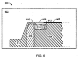
FIG. 6 illustrates a portion ofplasma processing apparatus 600. Theplasma processing apparatus 600 includes awafer processing chamber 602 having an electrostatic chuck (ESC) 604 (only one side of a cross section is shown). Thechuck 604 acts as an electrode and supports a wafer 606 (i.e. substrate) during fabrication. An inner RF couplededge ring 608 borders the edge of thechuck 604 and provides a RF coupled region that extends beyond the edge of thewafer 606. Anouter edge ring 610 borders the edges of the inner RF couplededge ring 608. AnRF coupler 612 is positioned below the inner RF couplededge ring 608 and borders an edge of thechuck 604. Adielectric filler 614 is positioned under the inner RF couplededge ring 608 and borders theRF coupler 612. A bottom surface of thedielectric filler 614 is adjacent to an upper edge of thechuck 604. - Advantageously,
dielectric filler 614 can provide even more flexibility in focusing the amount of RF electric energy that is RF coupled. Thedielectric filler 614 can minimize any coupling with respect to theouter edge ring 610. For example,dielectric filler 614 can be made of appropriate insulator material such as, Ceramic, Quartz, Teflon, and Polymer. The amount of insulation can also be controlled by choosing the thickness of the selected material for thedielectric filler 614. - A
dielectric filler 616 is positioned belowouter edge ring 610. Thedielectric filler 616 borders an outer edge of thechuck 106. Advantageously,dielectric filer 616 is positioned to isolate the RF poweredchuck 604 from a grounded region of anouter ground ring 618. Typically, theouter ground ring 618 is positioned in the vicinity of a wall of thewafer processing system 602. - As discussed with respect to
FIGs. 4 and5 , by providing an extended RF coupled region that extends beyond the edges ofwafer 606, a corrective action is performed on the sheath above thewafer 606. Consequently, the etch rate across the entire surface of thewafer 606 is more uniform than conventionally achieved and etched features at the peripheral regions do not suffer from "tilting" problems. In addition, by overlapping the gaps that may be present in the system,dielectric fillers chuck 604. - The various edge rings discussed above can be made using material that is relatively inexpensive and easy to manufacture and/or replace. This material can be chosen from a variety of material that are compatible to a particular etching process
- The invention has numerous advantages. One advantage of the invention is that etch rate uniformity across a substrate surface is significantly improved. Another advantage of the invention is that significant improvement in etch rate uniformity is achieved without risking contamination of the processing chamber. Yet another advantage is that tilting of etched features can be substantially eliminated.
- Although only an embodiment of the present invention has been described in detail, it should be understood that the present invention may be embodied in many other specific forms without departing from the scope of the invention. Therefore, the present examples are to be considered as illustrative and not restrictive, and the invention is not to be limited to the details given herein, but may be modified within the scope of the appended claims.
Claims (8)
- A plasma processing chamber (502) for etching a substrate (506), the substrate having a top surface, a bottom surface and an edge, said plasma processing chamber comprising:a radio frequency (RF) powered chuck (504), said RF powered chuck supporting at least a portion of the bottom surface of the substrate; andan inner RF coupler edge ring (508) placed over a portion of said RF powered chuck and adjacent to an edge of the substrate; whereinan RF coupler (514) is provided between said inner RF coupled edge ring and the portion of said RF powered chuck; whereina portion of RF energy provided by said RF powered chuck is coupled to said inner RF coupled edge ring through said RF coupler; characterised in thatsaid RF coupler is made from conductive material surrounded by a coating of dielectric material.
- The plasma processing chamber of claim 1, wherein said inner RF coupled edge ring surrounds the substrate.
- The plasma processing chamber of claim 1 or 2, wherein the substrate is a wafer.
- The plasma processing chamber of any preceding claim, wherein said plasma processing chamber further comprises:an outer edge ring (512) that surrounds said inner RF coupled edge ring.
- The plasma processing chamber of claim 4, wherein said outer edge ring further surrounds a portion of said RF powered chuck.
- The plasma processing chamber of any preceding claim, wherein said inner RF coupled edge ring and said RF coupler extend a predetermined distance from the edge of the substrate.
- The plasma processing chamber of any preceding claim, wherein said RF coupler is a metal with a dielectric coating.
- The plasma processing chamber of claim 7, wherein an amount of RF energy through said RF coupler from said RF power chuck to said inner RF coupled edge ring is directly proportional to the thickness of the dielectric coating.
Priority Applications (1)
| Application Number | Priority Date | Filing Date | Title |
|---|---|---|---|
| EP07023156A EP1898444B1 (en) | 1999-06-30 | 2000-06-29 | Plasma etching chamber |
Applications Claiming Priority (3)
| Application Number | Priority Date | Filing Date | Title |
|---|---|---|---|
| US09/345,639 US6344105B1 (en) | 1999-06-30 | 1999-06-30 | Techniques for improving etch rate uniformity |
| US345639 | 1999-06-30 | ||
| PCT/US2000/018234 WO2001001445A1 (en) | 1999-06-30 | 2000-06-29 | Techniques for improving etch rate uniformity |
Related Child Applications (1)
| Application Number | Title | Priority Date | Filing Date |
|---|---|---|---|
| EP07023156A Division EP1898444B1 (en) | 1999-06-30 | 2000-06-29 | Plasma etching chamber |
Publications (2)
| Publication Number | Publication Date |
|---|---|
| EP1198821A1 EP1198821A1 (en) | 2002-04-24 |
| EP1198821B1 true EP1198821B1 (en) | 2008-02-27 |
Family
ID=23355856
Family Applications (2)
| Application Number | Title | Priority Date | Filing Date |
|---|---|---|---|
| EP07023156A Expired - Lifetime EP1898444B1 (en) | 1999-06-30 | 2000-06-29 | Plasma etching chamber |
| EP00945097A Expired - Lifetime EP1198821B1 (en) | 1999-06-30 | 2000-06-29 | Plasma etching chamber |
Family Applications Before (1)
| Application Number | Title | Priority Date | Filing Date |
|---|---|---|---|
| EP07023156A Expired - Lifetime EP1898444B1 (en) | 1999-06-30 | 2000-06-29 | Plasma etching chamber |
Country Status (9)
| Country | Link |
|---|---|
| US (1) | US6344105B1 (en) |
| EP (2) | EP1898444B1 (en) |
| JP (2) | JP4792185B2 (en) |
| KR (1) | KR100743872B1 (en) |
| CN (2) | CN100392791C (en) |
| AU (1) | AU5908600A (en) |
| DE (2) | DE60038175T2 (en) |
| TW (1) | TW463235B (en) |
| WO (1) | WO2001001445A1 (en) |
Families Citing this family (108)
| Publication number | Priority date | Publication date | Assignee | Title |
|---|---|---|---|---|
| US5662770A (en) * | 1993-04-16 | 1997-09-02 | Micron Technology, Inc. | Method and apparatus for improving etch uniformity in remote source plasma reactors with powered wafer chucks |
| US6334960B1 (en) * | 1999-03-11 | 2002-01-01 | Board Of Regents, The University Of Texas System | Step and flash imprint lithography |
| KR100315088B1 (en) * | 1999-09-29 | 2001-11-24 | 윤종용 | Apparatus for processing semiconductor wafer having focus ring |
| US6489249B1 (en) * | 2000-06-20 | 2002-12-03 | Infineon Technologies Ag | Elimination/reduction of black silicon in DT etch |
| TW506234B (en) * | 2000-09-18 | 2002-10-11 | Tokyo Electron Ltd | Tunable focus ring for plasma processing |
| US6475336B1 (en) * | 2000-10-06 | 2002-11-05 | Lam Research Corporation | Electrostatically clamped edge ring for plasma processing |
| US6554954B2 (en) * | 2001-04-03 | 2003-04-29 | Applied Materials Inc. | Conductive collar surrounding semiconductor workpiece in plasma chamber |
| TWI234417B (en) * | 2001-07-10 | 2005-06-11 | Tokyo Electron Ltd | Plasma procesor and plasma processing method |
| DE10143718A1 (en) * | 2001-08-31 | 2003-03-27 | Infineon Technologies Ag | Mounting device for wafer in plasma etching plant has sealant introduced into free space between wafer and electrode |
| US7041201B2 (en) * | 2001-11-14 | 2006-05-09 | Applied Materials, Inc. | Sidewall magnet improving uniformity of inductively coupled plasma and shields used therewith |
| AU2002366921A1 (en) * | 2001-12-13 | 2003-07-09 | Tokyo Electron Limited | Ring mechanism, and plasma processing device using the ring mechanism |
| US20030159778A1 (en) * | 2002-02-27 | 2003-08-28 | Kunihiko Koroyasu | Plasma processing apparatus, protecting layer therefor and installation of protecting layer |
| US20040000375A1 (en) * | 2002-06-27 | 2004-01-01 | Taiwan Semiconductor Manufacturing Co., Ltd. | Plasma etch chamber equipped with multi-layer insert ring |
| US20040040663A1 (en) * | 2002-08-29 | 2004-03-04 | Ryujiro Udo | Plasma processing apparatus |
| US20040112862A1 (en) * | 2002-12-12 | 2004-06-17 | Molecular Imprints, Inc. | Planarization composition and method of patterning a substrate using the same |
| DE10260645B3 (en) * | 2002-12-23 | 2004-09-16 | Infineon Technologies Ag | Compensation frame for holding substrate for semiconducting manufacture has polygonal inner profile for holding substrate, area of upper main surface of frame with different widths at different points |
| US20040168613A1 (en) * | 2003-02-27 | 2004-09-02 | Molecular Imprints, Inc. | Composition and method to form a release layer |
| US7540935B2 (en) * | 2003-03-14 | 2009-06-02 | Lam Research Corporation | Plasma oxidation and removal of oxidized material |
| KR101141488B1 (en) * | 2003-03-21 | 2012-05-03 | 도쿄엘렉트론가부시키가이샤 | Method and apparatus for reducing substrate backside deposition during processing |
| US7049052B2 (en) * | 2003-05-09 | 2006-05-23 | Lam Research Corporation | Method providing an improved bi-layer photoresist pattern |
| US20040226516A1 (en) * | 2003-05-13 | 2004-11-18 | Daniel Timothy J. | Wafer pedestal cover |
| CN100463112C (en) * | 2003-05-30 | 2009-02-18 | 周星工程股份有限公司 | Apparatus for semiconductor device |
| US7157036B2 (en) * | 2003-06-17 | 2007-01-02 | Molecular Imprints, Inc | Method to reduce adhesion between a conformable region and a pattern of a mold |
| US20060108710A1 (en) * | 2004-11-24 | 2006-05-25 | Molecular Imprints, Inc. | Method to reduce adhesion between a conformable region and a mold |
| US20050160934A1 (en) * | 2004-01-23 | 2005-07-28 | Molecular Imprints, Inc. | Materials and methods for imprint lithography |
| US7307118B2 (en) * | 2004-11-24 | 2007-12-11 | Molecular Imprints, Inc. | Composition to reduce adhesion between a conformable region and a mold |
| US7658816B2 (en) | 2003-09-05 | 2010-02-09 | Tokyo Electron Limited | Focus ring and plasma processing apparatus |
| US7024105B2 (en) * | 2003-10-10 | 2006-04-04 | Applied Materials Inc. | Substrate heater assembly |
| US7122482B2 (en) | 2003-10-27 | 2006-10-17 | Molecular Imprints, Inc. | Methods for fabricating patterned features utilizing imprint lithography |
| US7244336B2 (en) * | 2003-12-17 | 2007-07-17 | Lam Research Corporation | Temperature controlled hot edge ring assembly for reducing plasma reactor etch rate drift |
| US7338578B2 (en) * | 2004-01-20 | 2008-03-04 | Taiwan Semiconductor Manufacturing Co., Ltd. | Step edge insert ring for etch chamber |
| US8076386B2 (en) * | 2004-02-23 | 2011-12-13 | Molecular Imprints, Inc. | Materials for imprint lithography |
| US20050189068A1 (en) * | 2004-02-27 | 2005-09-01 | Kawasaki Microelectronics, Inc. | Plasma processing apparatus and method of plasma processing |
| JP3981091B2 (en) * | 2004-03-01 | 2007-09-26 | 株式会社東芝 | Film-forming ring and semiconductor device manufacturing equipment |
| US20050193951A1 (en) * | 2004-03-08 | 2005-09-08 | Muneo Furuse | Plasma processing apparatus |
| JP2005303099A (en) | 2004-04-14 | 2005-10-27 | Hitachi High-Technologies Corp | Apparatus and method for plasma processing |
| US7282550B2 (en) * | 2004-08-16 | 2007-10-16 | Molecular Imprints, Inc. | Composition to provide a layer with uniform etch characteristics |
| US7939131B2 (en) | 2004-08-16 | 2011-05-10 | Molecular Imprints, Inc. | Method to provide a layer with uniform etch characteristics |
| US20060062922A1 (en) * | 2004-09-23 | 2006-03-23 | Molecular Imprints, Inc. | Polymerization technique to attenuate oxygen inhibition of solidification of liquids and composition therefor |
| US7578945B2 (en) * | 2004-09-27 | 2009-08-25 | Lam Research Corporation | Method and apparatus for tuning a set of plasma processing steps |
| US7138067B2 (en) * | 2004-09-27 | 2006-11-21 | Lam Research Corporation | Methods and apparatus for tuning a set of plasma processing steps |
| US7244311B2 (en) * | 2004-10-13 | 2007-07-17 | Lam Research Corporation | Heat transfer system for improved semiconductor processing uniformity |
| US20060081557A1 (en) * | 2004-10-18 | 2006-04-20 | Molecular Imprints, Inc. | Low-k dielectric functional imprinting materials |
| GB0424371D0 (en) * | 2004-11-04 | 2004-12-08 | Trikon Technologies Ltd | Shielding design for backside metal deposition |
| JP4336320B2 (en) * | 2005-02-25 | 2009-09-30 | キヤノンアネルバ株式会社 | Wafer holder |
| US9659758B2 (en) * | 2005-03-22 | 2017-05-23 | Honeywell International Inc. | Coils utilized in vapor deposition applications and methods of production |
| US20060219172A1 (en) * | 2005-04-05 | 2006-10-05 | Taiwan Semiconductor Manufacturing Co., Ltd. | PVD equipment and electrode and deposition ring thereof |
| KR100714896B1 (en) * | 2005-06-08 | 2007-05-04 | 삼성전자주식회사 | Focus ring of dry etching apparatus |
| US20060278520A1 (en) * | 2005-06-13 | 2006-12-14 | Lee Eal H | Use of DC magnetron sputtering systems |
| KR100688747B1 (en) | 2005-06-27 | 2007-03-02 | 동부일렉트로닉스 주식회사 | Apparatus and method for etching wafer edge |
| US8557351B2 (en) * | 2005-07-22 | 2013-10-15 | Molecular Imprints, Inc. | Method for adhering materials together |
| US7759407B2 (en) * | 2005-07-22 | 2010-07-20 | Molecular Imprints, Inc. | Composition for adhering materials together |
| US8808808B2 (en) | 2005-07-22 | 2014-08-19 | Molecular Imprints, Inc. | Method for imprint lithography utilizing an adhesion primer layer |
| CN101258784B (en) * | 2005-09-22 | 2011-03-30 | 积水化学工业株式会社 | Plasma processing device |
| KR100964775B1 (en) * | 2005-10-12 | 2010-06-21 | 파나소닉 주식회사 | Plasma processing apparatus and plasma processing method |
| US7651571B2 (en) * | 2005-12-22 | 2010-01-26 | Kyocera Corporation | Susceptor |
| JP2007250967A (en) * | 2006-03-17 | 2007-09-27 | Tokyo Electron Ltd | Plasma treating apparatus and method, and focus ring |
| US8635971B2 (en) * | 2006-03-31 | 2014-01-28 | Lam Research Corporation | Tunable uniformity in a plasma processing system |
| KR100809957B1 (en) * | 2006-09-20 | 2008-03-07 | 삼성전자주식회사 | Semiconductor etching device |
| US20080194113A1 (en) * | 2006-09-20 | 2008-08-14 | Samsung Electronics Co., Ltd. | Methods and apparatus for semiconductor etching including an electro static chuck |
| US20080110557A1 (en) * | 2006-11-15 | 2008-05-15 | Molecular Imprints, Inc. | Methods and Compositions for Providing Preferential Adhesion and Release of Adjacent Surfaces |
| US20080296261A1 (en) * | 2007-06-01 | 2008-12-04 | Nordson Corporation | Apparatus and methods for improving treatment uniformity in a plasma process |
| US7837827B2 (en) * | 2007-06-28 | 2010-11-23 | Lam Research Corporation | Edge ring arrangements for substrate processing |
| US8999106B2 (en) * | 2007-12-19 | 2015-04-07 | Applied Materials, Inc. | Apparatus and method for controlling edge performance in an inductively coupled plasma chamber |
| US20090194414A1 (en) * | 2008-01-31 | 2009-08-06 | Nolander Ira G | Modified sputtering target and deposition components, methods of production and uses thereof |
| US8409355B2 (en) * | 2008-04-24 | 2013-04-02 | Applied Materials, Inc. | Low profile process kit |
| US20100101729A1 (en) * | 2008-10-28 | 2010-04-29 | Applied Materials, Inc. | Process kit having reduced erosion sensitivity |
| KR101063588B1 (en) * | 2008-11-05 | 2011-09-07 | 주식회사 디엠에스 | Electrostatic chuck assembly with structure to extend the life of cover ring and improve the etching performance of plasma reactor |
| KR101540609B1 (en) * | 2009-02-24 | 2015-07-31 | 삼성전자 주식회사 | Apparatus for etching edge of wafer |
| KR101343502B1 (en) * | 2009-07-24 | 2013-12-19 | 엘지디스플레이 주식회사 | Coater chuck of coating apparatus |
| WO2011058851A1 (en) * | 2009-11-16 | 2011-05-19 | シャープ株式会社 | Dry etching apparatus and dry etching method |
| JP6285620B2 (en) * | 2011-08-26 | 2018-02-28 | 新光電気工業株式会社 | Electrostatic chuck and semiconductor / liquid crystal manufacturing equipment |
| US9376752B2 (en) * | 2012-04-06 | 2016-06-28 | Applied Materials, Inc. | Edge ring for a deposition chamber |
| KR20140101996A (en) * | 2013-02-13 | 2014-08-21 | 삼성전자주식회사 | Unit for supporting a substrate and apparatus for etching substrate using plasma with the same |
| US9997381B2 (en) * | 2013-02-18 | 2018-06-12 | Lam Research Corporation | Hybrid edge ring for plasma wafer processing |
| WO2015116245A1 (en) * | 2014-01-30 | 2015-08-06 | Applied Materials, Inc. | Gas confiner assembly for eliminating shadow frame |
| US10242848B2 (en) * | 2014-12-12 | 2019-03-26 | Lam Research Corporation | Carrier ring structure and chamber systems including the same |
| JP2016184610A (en) * | 2015-03-25 | 2016-10-20 | 株式会社東芝 | Upper electrode, edge ring and plasma processing apparatus |
| US10903055B2 (en) * | 2015-04-17 | 2021-01-26 | Applied Materials, Inc. | Edge ring for bevel polymer reduction |
| US10755902B2 (en) * | 2015-05-27 | 2020-08-25 | Tokyo Electron Limited | Plasma processing apparatus and focus ring |
| JP6570971B2 (en) * | 2015-05-27 | 2019-09-04 | 東京エレクトロン株式会社 | Plasma processing apparatus and focus ring |
| US10854492B2 (en) | 2015-08-18 | 2020-12-01 | Lam Research Corporation | Edge ring assembly for improving feature profile tilting at extreme edge of wafer |
| KR101722382B1 (en) * | 2016-01-08 | 2017-04-03 | 주식회사 윈텔 | Plasma Processing Apparatus |
| JP6888007B2 (en) * | 2016-01-26 | 2021-06-16 | アプライド マテリアルズ インコーポレイテッドApplied Materials,Incorporated | Wafer edge ring lifting solution |
| CN107316795B (en) * | 2016-04-26 | 2020-01-03 | 北京北方华创微电子装备有限公司 | Focusing ring and plasma processing device |
| US10163642B2 (en) * | 2016-06-30 | 2018-12-25 | Taiwan Semiconductor Manufacturing Company, Ltd. | Semiconductor device, method and tool of manufacture |
| JP2018006299A (en) | 2016-07-08 | 2018-01-11 | 東芝メモリ株式会社 | Processing object susceptor for plasma processing apparatus, plasma processing apparatus and plasma processing method |
| US20180122670A1 (en) * | 2016-11-01 | 2018-05-03 | Varian Semiconductor Equipment Associates, Inc. | Removable substrate plane structure ring |
| US10032661B2 (en) | 2016-11-18 | 2018-07-24 | Taiwan Semiconductor Manufacturing Company, Ltd. | Semiconductor device, method, and tool of manufacture |
| KR102205922B1 (en) * | 2017-03-31 | 2021-01-22 | 베이징 이타운 세미컨덕터 테크놀로지 컴퍼니 리미티드 | Prevents material deposition on the workpiece in the process |
| KR101966793B1 (en) * | 2017-05-17 | 2019-04-09 | 세메스 주식회사 | Substrate supporting unit and substrate processing apparatus comprising the same |
| JP6966286B2 (en) * | 2017-10-11 | 2021-11-10 | 東京エレクトロン株式会社 | Plasma processing device, focus ring elevation control method and focus ring elevation control program |
| US11183373B2 (en) | 2017-10-11 | 2021-11-23 | Honeywell International Inc. | Multi-patterned sputter traps and methods of making |
| KR102089949B1 (en) * | 2017-10-20 | 2020-03-19 | 세메스 주식회사 | Substrate treating apparatus component of substrate treating apparatus |
| JP2022502867A (en) * | 2018-10-18 | 2022-01-11 | ラム リサーチ コーポレーションLam Research Corporation | Lower Plasma Exclusion Area Ring for Bevel Etcha |
| JP7117734B2 (en) * | 2018-12-06 | 2022-08-15 | 東京エレクトロン株式会社 | Plasma processing apparatus and plasma processing method |
| US11551965B2 (en) * | 2018-12-07 | 2023-01-10 | Applied Materials, Inc. | Apparatus to reduce polymers deposition |
| KR102647177B1 (en) * | 2019-02-11 | 2024-03-15 | 삼성전자주식회사 | Plasma processing apparatus |
| WO2020257095A1 (en) * | 2019-06-18 | 2020-12-24 | Lam Research Corporation | Reduced diameter carrier ring hardware for substrate processing systems |
| TW202101647A (en) * | 2019-06-20 | 2021-01-01 | 美商康寧公司 | Carrier for back end of line processing |
| KR102214333B1 (en) | 2019-06-27 | 2021-02-10 | 세메스 주식회사 | Apparatus and method for treating substrate |
| CN112885690B (en) * | 2019-11-29 | 2023-10-20 | 中微半导体设备(上海)股份有限公司 | Plasma processing device |
| CN112992631B (en) * | 2019-12-16 | 2023-09-29 | 中微半导体设备(上海)股份有限公司 | Lower electrode assembly, installation method thereof and plasma processing device |
| CN111312630A (en) * | 2020-03-05 | 2020-06-19 | 锐捷光电科技(江苏)有限公司 | Method for improving etching uniformity of single sealing leather ring |
| JP7398988B2 (en) * | 2020-03-13 | 2023-12-15 | 東京エレクトロン株式会社 | sputtering equipment |
| KR102177146B1 (en) * | 2020-04-10 | 2020-11-10 | 비씨엔씨 주식회사 | Edge ring for plasma process chamber |
| US11380575B2 (en) | 2020-07-27 | 2022-07-05 | Applied Materials, Inc. | Film thickness uniformity improvement using edge ring and bias electrode geometry |
| CN113921365B (en) * | 2021-09-29 | 2024-03-26 | 北京北方华创微电子装备有限公司 | Semiconductor process equipment and edge protection mechanism thereof |
Family Cites Families (18)
| Publication number | Priority date | Publication date | Assignee | Title |
|---|---|---|---|---|
| JP2501948B2 (en) * | 1990-10-26 | 1996-05-29 | 三菱電機株式会社 | Plasma processing method and plasma processing apparatus |
| US5411624A (en) * | 1991-07-23 | 1995-05-02 | Tokyo Electron Limited | Magnetron plasma processing apparatus |
| KR100297358B1 (en) * | 1991-07-23 | 2001-11-30 | 히가시 데쓰로 | Plasma Etching Equipment |
| JPH0529270A (en) * | 1991-07-23 | 1993-02-05 | Tokyo Electron Ltd | Magnetron plasma processing device |
| US5662770A (en) | 1993-04-16 | 1997-09-02 | Micron Technology, Inc. | Method and apparatus for improving etch uniformity in remote source plasma reactors with powered wafer chucks |
| JP2638443B2 (en) | 1993-08-31 | 1997-08-06 | 日本電気株式会社 | Dry etching method and dry etching apparatus |
| KR100264445B1 (en) * | 1993-10-04 | 2000-11-01 | 히가시 데쓰로 | Plasma treatment equipment |
| US5463525A (en) | 1993-12-20 | 1995-10-31 | International Business Machines Corporation | Guard ring electrostatic chuck |
| JP3257741B2 (en) * | 1994-03-03 | 2002-02-18 | 東京エレクトロン株式会社 | Plasma etching apparatus and method |
| JP2659919B2 (en) | 1994-01-13 | 1997-09-30 | インターナショナル・ビジネス・マシーンズ・コーポレイション | Plasma device for correcting non-uniformity of plasma |
| US5891348A (en) | 1996-01-26 | 1999-04-06 | Applied Materials, Inc. | Process gas focusing apparatus and method |
| JPH09213683A (en) * | 1996-02-07 | 1997-08-15 | Sony Corp | Plasma etching device |
| US6113731A (en) * | 1997-01-02 | 2000-09-05 | Applied Materials, Inc. | Magnetically-enhanced plasma chamber with non-uniform magnetic field |
| WO1999014788A1 (en) | 1997-09-16 | 1999-03-25 | Applied Materials, Inc. | Shield or ring surrounding semiconductor workpiece in plasma chamber |
| US6074488A (en) | 1997-09-16 | 2000-06-13 | Applied Materials, Inc | Plasma chamber support having an electrically coupled collar ring |
| US6039836A (en) | 1997-12-19 | 2000-03-21 | Lam Research Corporation | Focus rings |
| KR100258984B1 (en) * | 1997-12-24 | 2000-08-01 | 윤종용 | Dry etching apparatus |
| US6117349A (en) * | 1998-08-28 | 2000-09-12 | Taiwan Semiconductor Manufacturing Company, Ltd. | Composite shadow ring equipped with a sacrificial inner ring |
-
1999
- 1999-06-30 US US09/345,639 patent/US6344105B1/en not_active Expired - Lifetime
-
2000
- 2000-06-28 TW TW089112761A patent/TW463235B/en not_active IP Right Cessation
- 2000-06-29 EP EP07023156A patent/EP1898444B1/en not_active Expired - Lifetime
- 2000-06-29 EP EP00945097A patent/EP1198821B1/en not_active Expired - Lifetime
- 2000-06-29 CN CNB008097933A patent/CN100392791C/en not_active Expired - Lifetime
- 2000-06-29 DE DE60038175T patent/DE60038175T2/en not_active Expired - Lifetime
- 2000-06-29 DE DE60044958T patent/DE60044958D1/en not_active Expired - Lifetime
- 2000-06-29 AU AU59086/00A patent/AU5908600A/en not_active Abandoned
- 2000-06-29 CN CN2008100852345A patent/CN101241846B/en not_active Expired - Lifetime
- 2000-06-29 KR KR1020017016518A patent/KR100743872B1/en active IP Right Grant
- 2000-06-29 JP JP2001506576A patent/JP4792185B2/en not_active Expired - Lifetime
- 2000-06-29 WO PCT/US2000/018234 patent/WO2001001445A1/en active IP Right Grant
-
2010
- 2010-10-21 JP JP2010236658A patent/JP2011014943A/en active Pending
Also Published As
| Publication number | Publication date |
|---|---|
| WO2001001445A1 (en) | 2001-01-04 |
| KR100743872B1 (en) | 2007-07-30 |
| JP2003503841A (en) | 2003-01-28 |
| KR20020041340A (en) | 2002-06-01 |
| JP4792185B2 (en) | 2011-10-12 |
| US6344105B1 (en) | 2002-02-05 |
| AU5908600A (en) | 2001-01-31 |
| CN101241846A (en) | 2008-08-13 |
| CN100392791C (en) | 2008-06-04 |
| EP1898444A1 (en) | 2008-03-12 |
| EP1898444B1 (en) | 2010-09-08 |
| DE60038175T2 (en) | 2009-03-12 |
| TW463235B (en) | 2001-11-11 |
| CN101241846B (en) | 2010-08-11 |
| DE60044958D1 (en) | 2010-10-21 |
| DE60038175D1 (en) | 2008-04-10 |
| JP2011014943A (en) | 2011-01-20 |
| EP1198821A1 (en) | 2002-04-24 |
| CN1373899A (en) | 2002-10-09 |
Similar Documents
| Publication | Publication Date | Title |
|---|---|---|
| EP1198821B1 (en) | Plasma etching chamber | |
| KR101342319B1 (en) | Integrated capacitive and inductive power sources for a plasma etching chamber | |
| EP1474264B1 (en) | A plasma processing apparatus and method | |
| KR101336479B1 (en) | Methods and apparatus for selective pre-coating of a plasma processing chamber | |
| TWI388242B (en) | Plasma confinement baffle and flow equalizer for enhanced magnetic control of plasma radial distribution | |
| KR100600898B1 (en) | Focus ring arrangement for substantially eliminating unconfined plasma in a plasma processing chamber | |
| EP1336191B1 (en) | Stepped upper electrode for plasma processing uniformity | |
| EP1446825B1 (en) | Apparatus and method for improving etch rate uniformity | |
| JP2002516030A (en) | Thin film electrostatic shield for induction plasma processing | |
| KR20080094794A (en) | Plasma processing reactor with multiple capacitive and inductive power sources | |
| EP1230668A2 (en) | Method and apparatus for producing uniform process rates | |
| KR20000057263A (en) | Method and apparatus for producing a uniform density plasma above a substrate | |
| JP4933692B2 (en) | Reduction of ion energy | |
| KR20020093841A (en) | Inductively Coupled Plasma Etching Apparatus | |
| JP3458912B2 (en) | Plasma processing equipment | |
| US20220051881A1 (en) | Plasma Etching Apparatus and Method | |
| JP4074168B2 (en) | Plasma processing equipment | |
| KR100603286B1 (en) | Antenna having multiple central axix and inductively coupled plasma generating apparatus applying the same | |
| CN112652511B (en) | Plasma etching device and edge ring therein |
Legal Events
| Date | Code | Title | Description |
|---|---|---|---|
| PUAI | Public reference made under article 153(3) epc to a published international application that has entered the european phase |
Free format text: ORIGINAL CODE: 0009012 |
|
| 17P | Request for examination filed |
Effective date: 20011227 |
|
| AK | Designated contracting states |
Kind code of ref document: A1 Designated state(s): AT BE CH CY DE DK ES FI FR GB GR IE IT LI LU MC NL PT SE |
|
| AX | Request for extension of the european patent |
Free format text: AL;LT;LV;MK;RO;SI |
|
| RBV | Designated contracting states (corrected) |
Designated state(s): DE FR GB IE |
|
| GRAC | Information related to communication of intention to grant a patent modified |
Free format text: ORIGINAL CODE: EPIDOSCIGR1 |
|
| GRAP | Despatch of communication of intention to grant a patent |
Free format text: ORIGINAL CODE: EPIDOSNIGR1 |
|
| RTI1 | Title (correction) |
Free format text: PLASMA ETCHING CHAMBER |
|
| GRAS | Grant fee paid |
Free format text: ORIGINAL CODE: EPIDOSNIGR3 |
|
| GRAA | (expected) grant |
Free format text: ORIGINAL CODE: 0009210 |
|
| AK | Designated contracting states |
Kind code of ref document: B1 Designated state(s): DE FR GB IE |
|
| REG | Reference to a national code |
Ref country code: GB Ref legal event code: FG4D |
|
| REG | Reference to a national code |
Ref country code: IE Ref legal event code: FG4D |
|
| REF | Corresponds to: |
Ref document number: 60038175 Country of ref document: DE Date of ref document: 20080410 Kind code of ref document: P |
|
| ET | Fr: translation filed | ||
| PLBE | No opposition filed within time limit |
Free format text: ORIGINAL CODE: 0009261 |
|
| STAA | Information on the status of an ep patent application or granted ep patent |
Free format text: STATUS: NO OPPOSITION FILED WITHIN TIME LIMIT |
|
| 26N | No opposition filed |
Effective date: 20081128 |
|
| GBPC | Gb: european patent ceased through non-payment of renewal fee |
Effective date: 20080629 |
|
| PG25 | Lapsed in a contracting state [announced via postgrant information from national office to epo] |
Ref country code: IE Free format text: LAPSE BECAUSE OF NON-PAYMENT OF DUE FEES Effective date: 20080630 |
|
| PG25 | Lapsed in a contracting state [announced via postgrant information from national office to epo] |
Ref country code: GB Free format text: LAPSE BECAUSE OF NON-PAYMENT OF DUE FEES Effective date: 20080629 |
|
| REG | Reference to a national code |
Ref country code: FR Ref legal event code: PLFP Year of fee payment: 17 |
|
| REG | Reference to a national code |
Ref country code: FR Ref legal event code: PLFP Year of fee payment: 18 |
|
| REG | Reference to a national code |
Ref country code: FR Ref legal event code: PLFP Year of fee payment: 19 |
|
| PGFP | Annual fee paid to national office [announced via postgrant information from national office to epo] |
Ref country code: FR Payment date: 20190625 Year of fee payment: 20 |
|
| PGFP | Annual fee paid to national office [announced via postgrant information from national office to epo] |
Ref country code: DE Payment date: 20190627 Year of fee payment: 20 |
|
| REG | Reference to a national code |
Ref country code: DE Ref legal event code: R071 Ref document number: 60038175 Country of ref document: DE |