EP1199746A2 - Resin-moulded semiconductor device with heat radiating electrode - Google Patents
Resin-moulded semiconductor device with heat radiating electrode Download PDFInfo
- Publication number
- EP1199746A2 EP1199746A2 EP20010302527 EP01302527A EP1199746A2 EP 1199746 A2 EP1199746 A2 EP 1199746A2 EP 20010302527 EP20010302527 EP 20010302527 EP 01302527 A EP01302527 A EP 01302527A EP 1199746 A2 EP1199746 A2 EP 1199746A2
- Authority
- EP
- European Patent Office
- Prior art keywords
- heat radiation
- radiation electrode
- semiconductor chip
- insulating resin
- semiconductor device
- Prior art date
- Legal status (The legal status is an assumption and is not a legal conclusion. Google has not performed a legal analysis and makes no representation as to the accuracy of the status listed.)
- Granted
Links
Images


Classifications
-
- H—ELECTRICITY
- H01—ELECTRIC ELEMENTS
- H01L—SEMICONDUCTOR DEVICES NOT COVERED BY CLASS H10
- H01L24/00—Arrangements for connecting or disconnecting semiconductor or solid-state bodies; Methods or apparatus related thereto
- H01L24/01—Means for bonding being attached to, or being formed on, the surface to be connected, e.g. chip-to-package, die-attach, "first-level" interconnects; Manufacturing methods related thereto
- H01L24/26—Layer connectors, e.g. plate connectors, solder or adhesive layers; Manufacturing methods related thereto
- H01L24/31—Structure, shape, material or disposition of the layer connectors after the connecting process
- H01L24/32—Structure, shape, material or disposition of the layer connectors after the connecting process of an individual layer connector
-
- H—ELECTRICITY
- H01—ELECTRIC ELEMENTS
- H01L—SEMICONDUCTOR DEVICES NOT COVERED BY CLASS H10
- H01L23/00—Details of semiconductor or other solid state devices
- H01L23/34—Arrangements for cooling, heating, ventilating or temperature compensation ; Temperature sensing arrangements
- H01L23/42—Fillings or auxiliary members in containers or encapsulations selected or arranged to facilitate heating or cooling
-
- G—PHYSICS
- G11—INFORMATION STORAGE
- G11B—INFORMATION STORAGE BASED ON RELATIVE MOVEMENT BETWEEN RECORD CARRIER AND TRANSDUCER
- G11B5/00—Recording by magnetisation or demagnetisation of a record carrier; Reproducing by magnetic means; Record carriers therefor
- G11B5/48—Disposition or mounting of heads or head supports relative to record carriers ; arrangements of heads, e.g. for scanning the record carrier to increase the relative speed
- G11B5/4806—Disposition or mounting of heads or head supports relative to record carriers ; arrangements of heads, e.g. for scanning the record carrier to increase the relative speed specially adapted for disk drive assemblies, e.g. assembly prior to operation, hard or flexible disk drives
- G11B5/4853—Constructional details of the electrical connection between head and arm
-
- H—ELECTRICITY
- H01—ELECTRIC ELEMENTS
- H01L—SEMICONDUCTOR DEVICES NOT COVERED BY CLASS H10
- H01L21/00—Processes or apparatus adapted for the manufacture or treatment of semiconductor or solid state devices or of parts thereof
- H01L21/02—Manufacture or treatment of semiconductor devices or of parts thereof
- H01L21/04—Manufacture or treatment of semiconductor devices or of parts thereof the devices having at least one potential-jump barrier or surface barrier, e.g. PN junction, depletion layer or carrier concentration layer
- H01L21/48—Manufacture or treatment of parts, e.g. containers, prior to assembly of the devices, using processes not provided for in a single one of the subgroups H01L21/06 - H01L21/326
- H01L21/4814—Conductive parts
- H01L21/4821—Flat leads, e.g. lead frames with or without insulating supports
- H01L21/4828—Etching
- H01L21/4832—Etching a temporary substrate after encapsulation process to form leads
-
- H—ELECTRICITY
- H01—ELECTRIC ELEMENTS
- H01L—SEMICONDUCTOR DEVICES NOT COVERED BY CLASS H10
- H01L21/00—Processes or apparatus adapted for the manufacture or treatment of semiconductor or solid state devices or of parts thereof
- H01L21/02—Manufacture or treatment of semiconductor devices or of parts thereof
- H01L21/04—Manufacture or treatment of semiconductor devices or of parts thereof the devices having at least one potential-jump barrier or surface barrier, e.g. PN junction, depletion layer or carrier concentration layer
- H01L21/50—Assembly of semiconductor devices using processes or apparatus not provided for in a single one of the subgroups H01L21/06 - H01L21/326, e.g. sealing of a cap to a base of a container
- H01L21/56—Encapsulations, e.g. encapsulation layers, coatings
- H01L21/563—Encapsulation of active face of flip-chip device, e.g. underfilling or underencapsulation of flip-chip, encapsulation preform on chip or mounting substrate
-
- H—ELECTRICITY
- H01—ELECTRIC ELEMENTS
- H01L—SEMICONDUCTOR DEVICES NOT COVERED BY CLASS H10
- H01L23/00—Details of semiconductor or other solid state devices
- H01L23/28—Encapsulations, e.g. encapsulating layers, coatings, e.g. for protection
- H01L23/31—Encapsulations, e.g. encapsulating layers, coatings, e.g. for protection characterised by the arrangement or shape
- H01L23/3107—Encapsulations, e.g. encapsulating layers, coatings, e.g. for protection characterised by the arrangement or shape the device being completely enclosed
- H01L23/3114—Encapsulations, e.g. encapsulating layers, coatings, e.g. for protection characterised by the arrangement or shape the device being completely enclosed the device being a chip scale package, e.g. CSP
-
- H—ELECTRICITY
- H01—ELECTRIC ELEMENTS
- H01L—SEMICONDUCTOR DEVICES NOT COVERED BY CLASS H10
- H01L23/00—Details of semiconductor or other solid state devices
- H01L23/28—Encapsulations, e.g. encapsulating layers, coatings, e.g. for protection
- H01L23/31—Encapsulations, e.g. encapsulating layers, coatings, e.g. for protection characterised by the arrangement or shape
- H01L23/3107—Encapsulations, e.g. encapsulating layers, coatings, e.g. for protection characterised by the arrangement or shape the device being completely enclosed
- H01L23/3135—Double encapsulation or coating and encapsulation
-
- H—ELECTRICITY
- H01—ELECTRIC ELEMENTS
- H01L—SEMICONDUCTOR DEVICES NOT COVERED BY CLASS H10
- H01L23/00—Details of semiconductor or other solid state devices
- H01L23/34—Arrangements for cooling, heating, ventilating or temperature compensation ; Temperature sensing arrangements
- H01L23/42—Fillings or auxiliary members in containers or encapsulations selected or arranged to facilitate heating or cooling
- H01L23/433—Auxiliary members in containers characterised by their shape, e.g. pistons
- H01L23/4334—Auxiliary members in encapsulations
-
- H—ELECTRICITY
- H01—ELECTRIC ELEMENTS
- H01L—SEMICONDUCTOR DEVICES NOT COVERED BY CLASS H10
- H01L24/00—Arrangements for connecting or disconnecting semiconductor or solid-state bodies; Methods or apparatus related thereto
- H01L24/93—Batch processes
- H01L24/95—Batch processes at chip-level, i.e. with connecting carried out on a plurality of singulated devices, i.e. on diced chips
- H01L24/97—Batch processes at chip-level, i.e. with connecting carried out on a plurality of singulated devices, i.e. on diced chips the devices being connected to a common substrate, e.g. interposer, said common substrate being separable into individual assemblies after connecting
-
- H—ELECTRICITY
- H05—ELECTRIC TECHNIQUES NOT OTHERWISE PROVIDED FOR
- H05K—PRINTED CIRCUITS; CASINGS OR CONSTRUCTIONAL DETAILS OF ELECTRIC APPARATUS; MANUFACTURE OF ASSEMBLAGES OF ELECTRICAL COMPONENTS
- H05K1/00—Printed circuits
- H05K1/02—Details
- H05K1/0201—Thermal arrangements, e.g. for cooling, heating or preventing overheating
- H05K1/0203—Cooling of mounted components
- H05K1/0204—Cooling of mounted components using means for thermal conduction connection in the thickness direction of the substrate
-
- H—ELECTRICITY
- H05—ELECTRIC TECHNIQUES NOT OTHERWISE PROVIDED FOR
- H05K—PRINTED CIRCUITS; CASINGS OR CONSTRUCTIONAL DETAILS OF ELECTRIC APPARATUS; MANUFACTURE OF ASSEMBLAGES OF ELECTRICAL COMPONENTS
- H05K1/00—Printed circuits
- H05K1/02—Details
- H05K1/0201—Thermal arrangements, e.g. for cooling, heating or preventing overheating
- H05K1/0203—Cooling of mounted components
- H05K1/021—Components thermally connected to metal substrates or heat-sinks by insert mounting
-
- H—ELECTRICITY
- H01—ELECTRIC ELEMENTS
- H01L—SEMICONDUCTOR DEVICES NOT COVERED BY CLASS H10
- H01L2224/00—Indexing scheme for arrangements for connecting or disconnecting semiconductor or solid-state bodies and methods related thereto as covered by H01L24/00
- H01L2224/01—Means for bonding being attached to, or being formed on, the surface to be connected, e.g. chip-to-package, die-attach, "first-level" interconnects; Manufacturing methods related thereto
- H01L2224/02—Bonding areas; Manufacturing methods related thereto
- H01L2224/04—Structure, shape, material or disposition of the bonding areas prior to the connecting process
- H01L2224/05—Structure, shape, material or disposition of the bonding areas prior to the connecting process of an individual bonding area
- H01L2224/0554—External layer
- H01L2224/05599—Material
-
- H—ELECTRICITY
- H01—ELECTRIC ELEMENTS
- H01L—SEMICONDUCTOR DEVICES NOT COVERED BY CLASS H10
- H01L2224/00—Indexing scheme for arrangements for connecting or disconnecting semiconductor or solid-state bodies and methods related thereto as covered by H01L24/00
- H01L2224/01—Means for bonding being attached to, or being formed on, the surface to be connected, e.g. chip-to-package, die-attach, "first-level" interconnects; Manufacturing methods related thereto
- H01L2224/10—Bump connectors; Manufacturing methods related thereto
- H01L2224/15—Structure, shape, material or disposition of the bump connectors after the connecting process
- H01L2224/16—Structure, shape, material or disposition of the bump connectors after the connecting process of an individual bump connector
-
- H—ELECTRICITY
- H01—ELECTRIC ELEMENTS
- H01L—SEMICONDUCTOR DEVICES NOT COVERED BY CLASS H10
- H01L2224/00—Indexing scheme for arrangements for connecting or disconnecting semiconductor or solid-state bodies and methods related thereto as covered by H01L24/00
- H01L2224/01—Means for bonding being attached to, or being formed on, the surface to be connected, e.g. chip-to-package, die-attach, "first-level" interconnects; Manufacturing methods related thereto
- H01L2224/26—Layer connectors, e.g. plate connectors, solder or adhesive layers; Manufacturing methods related thereto
- H01L2224/31—Structure, shape, material or disposition of the layer connectors after the connecting process
- H01L2224/32—Structure, shape, material or disposition of the layer connectors after the connecting process of an individual layer connector
- H01L2224/3201—Structure
- H01L2224/32012—Structure relative to the bonding area, e.g. bond pad
- H01L2224/32013—Structure relative to the bonding area, e.g. bond pad the layer connector being larger than the bonding area, e.g. bond pad
-
- H—ELECTRICITY
- H01—ELECTRIC ELEMENTS
- H01L—SEMICONDUCTOR DEVICES NOT COVERED BY CLASS H10
- H01L2224/00—Indexing scheme for arrangements for connecting or disconnecting semiconductor or solid-state bodies and methods related thereto as covered by H01L24/00
- H01L2224/01—Means for bonding being attached to, or being formed on, the surface to be connected, e.g. chip-to-package, die-attach, "first-level" interconnects; Manufacturing methods related thereto
- H01L2224/26—Layer connectors, e.g. plate connectors, solder or adhesive layers; Manufacturing methods related thereto
- H01L2224/31—Structure, shape, material or disposition of the layer connectors after the connecting process
- H01L2224/32—Structure, shape, material or disposition of the layer connectors after the connecting process of an individual layer connector
- H01L2224/3205—Shape
- H01L2224/32057—Shape in side view
- H01L2224/32059—Shape in side view comprising protrusions or indentations
-
- H—ELECTRICITY
- H01—ELECTRIC ELEMENTS
- H01L—SEMICONDUCTOR DEVICES NOT COVERED BY CLASS H10
- H01L2224/00—Indexing scheme for arrangements for connecting or disconnecting semiconductor or solid-state bodies and methods related thereto as covered by H01L24/00
- H01L2224/01—Means for bonding being attached to, or being formed on, the surface to be connected, e.g. chip-to-package, die-attach, "first-level" interconnects; Manufacturing methods related thereto
- H01L2224/42—Wire connectors; Manufacturing methods related thereto
- H01L2224/44—Structure, shape, material or disposition of the wire connectors prior to the connecting process
- H01L2224/45—Structure, shape, material or disposition of the wire connectors prior to the connecting process of an individual wire connector
- H01L2224/45001—Core members of the connector
- H01L2224/45099—Material
-
- H—ELECTRICITY
- H01—ELECTRIC ELEMENTS
- H01L—SEMICONDUCTOR DEVICES NOT COVERED BY CLASS H10
- H01L2224/00—Indexing scheme for arrangements for connecting or disconnecting semiconductor or solid-state bodies and methods related thereto as covered by H01L24/00
- H01L2224/01—Means for bonding being attached to, or being formed on, the surface to be connected, e.g. chip-to-package, die-attach, "first-level" interconnects; Manufacturing methods related thereto
- H01L2224/42—Wire connectors; Manufacturing methods related thereto
- H01L2224/47—Structure, shape, material or disposition of the wire connectors after the connecting process
- H01L2224/48—Structure, shape, material or disposition of the wire connectors after the connecting process of an individual wire connector
- H01L2224/4805—Shape
- H01L2224/4809—Loop shape
- H01L2224/48091—Arched
-
- H—ELECTRICITY
- H01—ELECTRIC ELEMENTS
- H01L—SEMICONDUCTOR DEVICES NOT COVERED BY CLASS H10
- H01L2224/00—Indexing scheme for arrangements for connecting or disconnecting semiconductor or solid-state bodies and methods related thereto as covered by H01L24/00
- H01L2224/01—Means for bonding being attached to, or being formed on, the surface to be connected, e.g. chip-to-package, die-attach, "first-level" interconnects; Manufacturing methods related thereto
- H01L2224/42—Wire connectors; Manufacturing methods related thereto
- H01L2224/47—Structure, shape, material or disposition of the wire connectors after the connecting process
- H01L2224/48—Structure, shape, material or disposition of the wire connectors after the connecting process of an individual wire connector
- H01L2224/481—Disposition
- H01L2224/48151—Connecting between a semiconductor or solid-state body and an item not being a semiconductor or solid-state body, e.g. chip-to-substrate, chip-to-passive
- H01L2224/48221—Connecting between a semiconductor or solid-state body and an item not being a semiconductor or solid-state body, e.g. chip-to-substrate, chip-to-passive the body and the item being stacked
- H01L2224/48245—Connecting between a semiconductor or solid-state body and an item not being a semiconductor or solid-state body, e.g. chip-to-substrate, chip-to-passive the body and the item being stacked the item being metallic
- H01L2224/48247—Connecting between a semiconductor or solid-state body and an item not being a semiconductor or solid-state body, e.g. chip-to-substrate, chip-to-passive the body and the item being stacked the item being metallic connecting the wire to a bond pad of the item
-
- H—ELECTRICITY
- H01—ELECTRIC ELEMENTS
- H01L—SEMICONDUCTOR DEVICES NOT COVERED BY CLASS H10
- H01L2224/00—Indexing scheme for arrangements for connecting or disconnecting semiconductor or solid-state bodies and methods related thereto as covered by H01L24/00
- H01L2224/73—Means for bonding being of different types provided for in two or more of groups H01L2224/10, H01L2224/18, H01L2224/26, H01L2224/34, H01L2224/42, H01L2224/50, H01L2224/63, H01L2224/71
- H01L2224/732—Location after the connecting process
- H01L2224/73201—Location after the connecting process on the same surface
- H01L2224/73203—Bump and layer connectors
- H01L2224/73204—Bump and layer connectors the bump connector being embedded into the layer connector
-
- H—ELECTRICITY
- H01—ELECTRIC ELEMENTS
- H01L—SEMICONDUCTOR DEVICES NOT COVERED BY CLASS H10
- H01L2224/00—Indexing scheme for arrangements for connecting or disconnecting semiconductor or solid-state bodies and methods related thereto as covered by H01L24/00
- H01L2224/80—Methods for connecting semiconductor or other solid state bodies using means for bonding being attached to, or being formed on, the surface to be connected
- H01L2224/83—Methods for connecting semiconductor or other solid state bodies using means for bonding being attached to, or being formed on, the surface to be connected using a layer connector
- H01L2224/8338—Bonding interfaces outside the semiconductor or solid-state body
- H01L2224/83385—Shape, e.g. interlocking features
-
- H—ELECTRICITY
- H01—ELECTRIC ELEMENTS
- H01L—SEMICONDUCTOR DEVICES NOT COVERED BY CLASS H10
- H01L2224/00—Indexing scheme for arrangements for connecting or disconnecting semiconductor or solid-state bodies and methods related thereto as covered by H01L24/00
- H01L2224/80—Methods for connecting semiconductor or other solid state bodies using means for bonding being attached to, or being formed on, the surface to be connected
- H01L2224/85—Methods for connecting semiconductor or other solid state bodies using means for bonding being attached to, or being formed on, the surface to be connected using a wire connector
- H01L2224/8538—Bonding interfaces outside the semiconductor or solid-state body
- H01L2224/85399—Material
-
- H—ELECTRICITY
- H01—ELECTRIC ELEMENTS
- H01L—SEMICONDUCTOR DEVICES NOT COVERED BY CLASS H10
- H01L2224/00—Indexing scheme for arrangements for connecting or disconnecting semiconductor or solid-state bodies and methods related thereto as covered by H01L24/00
- H01L2224/93—Batch processes
- H01L2224/95—Batch processes at chip-level, i.e. with connecting carried out on a plurality of singulated devices, i.e. on diced chips
- H01L2224/97—Batch processes at chip-level, i.e. with connecting carried out on a plurality of singulated devices, i.e. on diced chips the devices being connected to a common substrate, e.g. interposer, said common substrate being separable into individual assemblies after connecting
-
- H—ELECTRICITY
- H01—ELECTRIC ELEMENTS
- H01L—SEMICONDUCTOR DEVICES NOT COVERED BY CLASS H10
- H01L24/00—Arrangements for connecting or disconnecting semiconductor or solid-state bodies; Methods or apparatus related thereto
- H01L24/01—Means for bonding being attached to, or being formed on, the surface to be connected, e.g. chip-to-package, die-attach, "first-level" interconnects; Manufacturing methods related thereto
- H01L24/42—Wire connectors; Manufacturing methods related thereto
- H01L24/47—Structure, shape, material or disposition of the wire connectors after the connecting process
- H01L24/48—Structure, shape, material or disposition of the wire connectors after the connecting process of an individual wire connector
-
- H—ELECTRICITY
- H01—ELECTRIC ELEMENTS
- H01L—SEMICONDUCTOR DEVICES NOT COVERED BY CLASS H10
- H01L2924/00—Indexing scheme for arrangements or methods for connecting or disconnecting semiconductor or solid-state bodies as covered by H01L24/00
- H01L2924/0001—Technical content checked by a classifier
- H01L2924/00014—Technical content checked by a classifier the subject-matter covered by the group, the symbol of which is combined with the symbol of this group, being disclosed without further technical details
-
- H—ELECTRICITY
- H01—ELECTRIC ELEMENTS
- H01L—SEMICONDUCTOR DEVICES NOT COVERED BY CLASS H10
- H01L2924/00—Indexing scheme for arrangements or methods for connecting or disconnecting semiconductor or solid-state bodies as covered by H01L24/00
- H01L2924/01—Chemical elements
- H01L2924/01005—Boron [B]
-
- H—ELECTRICITY
- H01—ELECTRIC ELEMENTS
- H01L—SEMICONDUCTOR DEVICES NOT COVERED BY CLASS H10
- H01L2924/00—Indexing scheme for arrangements or methods for connecting or disconnecting semiconductor or solid-state bodies as covered by H01L24/00
- H01L2924/01—Chemical elements
- H01L2924/01006—Carbon [C]
-
- H—ELECTRICITY
- H01—ELECTRIC ELEMENTS
- H01L—SEMICONDUCTOR DEVICES NOT COVERED BY CLASS H10
- H01L2924/00—Indexing scheme for arrangements or methods for connecting or disconnecting semiconductor or solid-state bodies as covered by H01L24/00
- H01L2924/01—Chemical elements
- H01L2924/01013—Aluminum [Al]
-
- H—ELECTRICITY
- H01—ELECTRIC ELEMENTS
- H01L—SEMICONDUCTOR DEVICES NOT COVERED BY CLASS H10
- H01L2924/00—Indexing scheme for arrangements or methods for connecting or disconnecting semiconductor or solid-state bodies as covered by H01L24/00
- H01L2924/01—Chemical elements
- H01L2924/01029—Copper [Cu]
-
- H—ELECTRICITY
- H01—ELECTRIC ELEMENTS
- H01L—SEMICONDUCTOR DEVICES NOT COVERED BY CLASS H10
- H01L2924/00—Indexing scheme for arrangements or methods for connecting or disconnecting semiconductor or solid-state bodies as covered by H01L24/00
- H01L2924/01—Chemical elements
- H01L2924/01033—Arsenic [As]
-
- H—ELECTRICITY
- H01—ELECTRIC ELEMENTS
- H01L—SEMICONDUCTOR DEVICES NOT COVERED BY CLASS H10
- H01L2924/00—Indexing scheme for arrangements or methods for connecting or disconnecting semiconductor or solid-state bodies as covered by H01L24/00
- H01L2924/01—Chemical elements
- H01L2924/01046—Palladium [Pd]
-
- H—ELECTRICITY
- H01—ELECTRIC ELEMENTS
- H01L—SEMICONDUCTOR DEVICES NOT COVERED BY CLASS H10
- H01L2924/00—Indexing scheme for arrangements or methods for connecting or disconnecting semiconductor or solid-state bodies as covered by H01L24/00
- H01L2924/01—Chemical elements
- H01L2924/01047—Silver [Ag]
-
- H—ELECTRICITY
- H01—ELECTRIC ELEMENTS
- H01L—SEMICONDUCTOR DEVICES NOT COVERED BY CLASS H10
- H01L2924/00—Indexing scheme for arrangements or methods for connecting or disconnecting semiconductor or solid-state bodies as covered by H01L24/00
- H01L2924/01—Chemical elements
- H01L2924/0105—Tin [Sn]
-
- H—ELECTRICITY
- H01—ELECTRIC ELEMENTS
- H01L—SEMICONDUCTOR DEVICES NOT COVERED BY CLASS H10
- H01L2924/00—Indexing scheme for arrangements or methods for connecting or disconnecting semiconductor or solid-state bodies as covered by H01L24/00
- H01L2924/01—Chemical elements
- H01L2924/01059—Praseodymium [Pr]
-
- H—ELECTRICITY
- H01—ELECTRIC ELEMENTS
- H01L—SEMICONDUCTOR DEVICES NOT COVERED BY CLASS H10
- H01L2924/00—Indexing scheme for arrangements or methods for connecting or disconnecting semiconductor or solid-state bodies as covered by H01L24/00
- H01L2924/01—Chemical elements
- H01L2924/01075—Rhenium [Re]
-
- H—ELECTRICITY
- H01—ELECTRIC ELEMENTS
- H01L—SEMICONDUCTOR DEVICES NOT COVERED BY CLASS H10
- H01L2924/00—Indexing scheme for arrangements or methods for connecting or disconnecting semiconductor or solid-state bodies as covered by H01L24/00
- H01L2924/01—Chemical elements
- H01L2924/01078—Platinum [Pt]
-
- H—ELECTRICITY
- H01—ELECTRIC ELEMENTS
- H01L—SEMICONDUCTOR DEVICES NOT COVERED BY CLASS H10
- H01L2924/00—Indexing scheme for arrangements or methods for connecting or disconnecting semiconductor or solid-state bodies as covered by H01L24/00
- H01L2924/01—Chemical elements
- H01L2924/01079—Gold [Au]
-
- H—ELECTRICITY
- H01—ELECTRIC ELEMENTS
- H01L—SEMICONDUCTOR DEVICES NOT COVERED BY CLASS H10
- H01L2924/00—Indexing scheme for arrangements or methods for connecting or disconnecting semiconductor or solid-state bodies as covered by H01L24/00
- H01L2924/01—Chemical elements
- H01L2924/01082—Lead [Pb]
-
- H—ELECTRICITY
- H01—ELECTRIC ELEMENTS
- H01L—SEMICONDUCTOR DEVICES NOT COVERED BY CLASS H10
- H01L2924/00—Indexing scheme for arrangements or methods for connecting or disconnecting semiconductor or solid-state bodies as covered by H01L24/00
- H01L2924/013—Alloys
- H01L2924/0132—Binary Alloys
-
- H—ELECTRICITY
- H01—ELECTRIC ELEMENTS
- H01L—SEMICONDUCTOR DEVICES NOT COVERED BY CLASS H10
- H01L2924/00—Indexing scheme for arrangements or methods for connecting or disconnecting semiconductor or solid-state bodies as covered by H01L24/00
- H01L2924/06—Polymers
- H01L2924/078—Adhesive characteristics other than chemical
- H01L2924/07802—Adhesive characteristics other than chemical not being an ohmic electrical conductor
-
- H—ELECTRICITY
- H01—ELECTRIC ELEMENTS
- H01L—SEMICONDUCTOR DEVICES NOT COVERED BY CLASS H10
- H01L2924/00—Indexing scheme for arrangements or methods for connecting or disconnecting semiconductor or solid-state bodies as covered by H01L24/00
- H01L2924/10—Details of semiconductor or other solid state devices to be connected
- H01L2924/11—Device type
- H01L2924/12—Passive devices, e.g. 2 terminal devices
- H01L2924/1204—Optical Diode
- H01L2924/12042—LASER
-
- H—ELECTRICITY
- H01—ELECTRIC ELEMENTS
- H01L—SEMICONDUCTOR DEVICES NOT COVERED BY CLASS H10
- H01L2924/00—Indexing scheme for arrangements or methods for connecting or disconnecting semiconductor or solid-state bodies as covered by H01L24/00
- H01L2924/10—Details of semiconductor or other solid state devices to be connected
- H01L2924/11—Device type
- H01L2924/12—Passive devices, e.g. 2 terminal devices
- H01L2924/1204—Optical Diode
- H01L2924/12044—OLED
-
- H—ELECTRICITY
- H01—ELECTRIC ELEMENTS
- H01L—SEMICONDUCTOR DEVICES NOT COVERED BY CLASS H10
- H01L2924/00—Indexing scheme for arrangements or methods for connecting or disconnecting semiconductor or solid-state bodies as covered by H01L24/00
- H01L2924/10—Details of semiconductor or other solid state devices to be connected
- H01L2924/11—Device type
- H01L2924/14—Integrated circuits
- H01L2924/143—Digital devices
- H01L2924/1433—Application-specific integrated circuit [ASIC]
-
- H—ELECTRICITY
- H01—ELECTRIC ELEMENTS
- H01L—SEMICONDUCTOR DEVICES NOT COVERED BY CLASS H10
- H01L2924/00—Indexing scheme for arrangements or methods for connecting or disconnecting semiconductor or solid-state bodies as covered by H01L24/00
- H01L2924/15—Details of package parts other than the semiconductor or other solid state devices to be connected
- H01L2924/151—Die mounting substrate
- H01L2924/153—Connection portion
- H01L2924/1531—Connection portion the connection portion being formed only on the surface of the substrate opposite to the die mounting surface
- H01L2924/15311—Connection portion the connection portion being formed only on the surface of the substrate opposite to the die mounting surface being a ball array, e.g. BGA
-
- H—ELECTRICITY
- H01—ELECTRIC ELEMENTS
- H01L—SEMICONDUCTOR DEVICES NOT COVERED BY CLASS H10
- H01L2924/00—Indexing scheme for arrangements or methods for connecting or disconnecting semiconductor or solid-state bodies as covered by H01L24/00
- H01L2924/15—Details of package parts other than the semiconductor or other solid state devices to be connected
- H01L2924/151—Die mounting substrate
- H01L2924/156—Material
- H01L2924/15786—Material with a principal constituent of the material being a non metallic, non metalloid inorganic material
- H01L2924/15787—Ceramics, e.g. crystalline carbides, nitrides or oxides
-
- H—ELECTRICITY
- H01—ELECTRIC ELEMENTS
- H01L—SEMICONDUCTOR DEVICES NOT COVERED BY CLASS H10
- H01L2924/00—Indexing scheme for arrangements or methods for connecting or disconnecting semiconductor or solid-state bodies as covered by H01L24/00
- H01L2924/15—Details of package parts other than the semiconductor or other solid state devices to be connected
- H01L2924/181—Encapsulation
-
- H—ELECTRICITY
- H01—ELECTRIC ELEMENTS
- H01L—SEMICONDUCTOR DEVICES NOT COVERED BY CLASS H10
- H01L2924/00—Indexing scheme for arrangements or methods for connecting or disconnecting semiconductor or solid-state bodies as covered by H01L24/00
- H01L2924/30—Technical effects
- H01L2924/301—Electrical effects
- H01L2924/3011—Impedance
-
- H—ELECTRICITY
- H01—ELECTRIC ELEMENTS
- H01L—SEMICONDUCTOR DEVICES NOT COVERED BY CLASS H10
- H01L2924/00—Indexing scheme for arrangements or methods for connecting or disconnecting semiconductor or solid-state bodies as covered by H01L24/00
- H01L2924/30—Technical effects
- H01L2924/35—Mechanical effects
- H01L2924/351—Thermal stress
-
- H—ELECTRICITY
- H05—ELECTRIC TECHNIQUES NOT OTHERWISE PROVIDED FOR
- H05K—PRINTED CIRCUITS; CASINGS OR CONSTRUCTIONAL DETAILS OF ELECTRIC APPARATUS; MANUFACTURE OF ASSEMBLAGES OF ELECTRICAL COMPONENTS
- H05K1/00—Printed circuits
- H05K1/18—Printed circuits structurally associated with non-printed electric components
- H05K1/182—Printed circuits structurally associated with non-printed electric components associated with components mounted in the printed circuit board, e.g. insert mounted components [IMC]
-
- H—ELECTRICITY
- H05—ELECTRIC TECHNIQUES NOT OTHERWISE PROVIDED FOR
- H05K—PRINTED CIRCUITS; CASINGS OR CONSTRUCTIONAL DETAILS OF ELECTRIC APPARATUS; MANUFACTURE OF ASSEMBLAGES OF ELECTRICAL COMPONENTS
- H05K1/00—Printed circuits
- H05K1/18—Printed circuits structurally associated with non-printed electric components
- H05K1/189—Printed circuits structurally associated with non-printed electric components characterised by the use of a flexible or folded printed circuit
-
- H—ELECTRICITY
- H05—ELECTRIC TECHNIQUES NOT OTHERWISE PROVIDED FOR
- H05K—PRINTED CIRCUITS; CASINGS OR CONSTRUCTIONAL DETAILS OF ELECTRIC APPARATUS; MANUFACTURE OF ASSEMBLAGES OF ELECTRICAL COMPONENTS
- H05K2201/00—Indexing scheme relating to printed circuits covered by H05K1/00
- H05K2201/10—Details of components or other objects attached to or integrated in a printed circuit board
- H05K2201/10227—Other objects, e.g. metallic pieces
- H05K2201/10416—Metallic blocks or heatsinks completely inserted in a PCB
-
- H—ELECTRICITY
- H05—ELECTRIC TECHNIQUES NOT OTHERWISE PROVIDED FOR
- H05K—PRINTED CIRCUITS; CASINGS OR CONSTRUCTIONAL DETAILS OF ELECTRIC APPARATUS; MANUFACTURE OF ASSEMBLAGES OF ELECTRICAL COMPONENTS
- H05K2201/00—Indexing scheme relating to printed circuits covered by H05K1/00
- H05K2201/10—Details of components or other objects attached to or integrated in a printed circuit board
- H05K2201/10613—Details of electrical connections of non-printed components, e.g. special leads
- H05K2201/10621—Components characterised by their electrical contacts
- H05K2201/10727—Leadless chip carrier [LCC], e.g. chip-modules for cards
Definitions
- the present invention relates to a semiconductor device, a semiconductor module and a hard disk, and especially to a structure capable of efficiently dissipating heat from a semiconductor chip.
- semiconductor devices are mounted on various types of substrates, which, in turn, are mounted in various many systems as semiconductor modules.
- a substrate the use of a ceramic substrate, a printed board, a flexible sheet, a metal substrate or a glass substrate etc. may be contemplated, and the following description gives one example thereof.
- the semiconductor module is explained as being mounted on a flexible sheet.
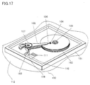
- Fig. 17 shows an example in which a semiconductor module using a flexible sheet is mounted in a hard disk 100.
- This hard disk 100 may be, for example, the one described in detail in an article of Nikkei Electronics (No. 691, June 16, 1997, p.92-).
- This hard disk 100 is accommodated within a casing 101 made of a metal, and comprises a plurality of recording disks 102 that are integrally attached to a spindle motor 103. Over the surfaces of individual recording disks 102, magnetic heads 104 are respectively disposed each with a very small clearance. These magnetic heads 104 are attached at the tips of suspensions 106 which are affixed to the ends of respective arms 105. A magnetic head 104, a suspension 106 and an arm 105 together form one integral body and this integral body is attached to an actuator 107.
- the magnetic heads 104 must be electrically connected with a read/write amplifying IC 108 in order to perform read and write operations . Accordingly, a semiconductor module comprising this read/write amplifying IC 108 mounted on a flexible sheet 109 is used, and the wirings provided on this flexible sheet 109 are electrically connected, ultimately, to the magnetic heads 104.
- This semiconductor module 110 is called “flexible circuit assembly”, typically abbreviated as "FCA”.
- connectors 111 provided on the semiconductor module 110 are exposed, and these connector (male or female) 111 and connectors (female or male) attached on a main board 112 are engaged.
- main board 112 wirings are provided, and driving ICs for the spindle motor 103, a buffer memory and other ICs for a driving, such as ASIC, are mounted.
- the recording disk 102 spins at, for example, 4500rpm via the spindle motor 103, and the actuator 107 detects the position of the magnetic head 104. Since this spinning mechanism is enclosed by a cover provided over the casing 101, there is no way to completely prevent the accumulation of heat, resulting in the temperature rise in the read/write amplifying IC 108. Therefore, the read/write amplifying IC 108 is attached to the actuator 107 or the casing 101 etc. at a location having a better heat conduction property than elsewhere. Further, since revolutions of the spindle motor 103 tend to high speed such as 5400, 7200 and 10000 rpm, this heat dissipation has more importance.
- Fig. 18A is the plan view
- Fig. 18B is a cross-sectional view taken along the line A-A which cuts across the read/write amplifying IC 108 provided on one end of the module.
- This FCA 110 is attached to an internal portion of the casing 101 in a folded-state, so that it employs a first flexible sheet 109 have a two-dimensional shape that can easily be folded.
- the connectors 111 are attached, forming a first connection section 120.
- First wirings 121 electrically connected to these connectors 111 are adhered on the first flexible sheet 109, and they extend all the way to the right end.
- the first wirings 121 are then electrically connected to the read/write amplifying IC 108.
- Leads 122 of the read/write amplifying IC 108 to be connected to the magnetic heads 104 are connected with second wirings 123 which, in turn, are electrically connected to third wirings 126 on a second flexible sheet 124 provided over the arm 105 and suspension 106.
- the right end of the first flexible sheet 109 forms a second connection section 127 at which the first flexible sheet 109 is connected to the second flexible sheet 124.
- the first flexible sheet 109 and the second flexible sheet 124 may be integrally formed.
- the second wirings 123 and the third wirings 126 are provided integrally.
- a supporting member 128 is disposed on the back surface of the first flexible sheet 109 on which the read/write amplifying IC 108 is to be provided.
- the read/write amplifying IC 108 is thermally coupled with a metal that is exposed to inside of the casing 101 through this supporting member 128, so that the heat generated in the read/write amplifying IC 108 can be externally released.
- This flexible sheet 109 is constituted by laminating, from the bottom, a first polyimide sheet 130 (first PI sheet), a first adhesion layer 131, a conductive pattern 132, a second adhesion layer 133 and a second polyimide sheet 134 (second PI sheet), so that the conductive pattern 132 is sandwiched between the first and second PI sheets 130 and 134.
- a portion of the second PI sheet 134 and the second adhesion layer 133 are eliminated at a desired location to form an opening 135 which exposes the conductive pattern 132.
- the read/write amplifying IC 108 is electrically connected thereto through leads 122 as shown in the figure.
- the semiconductor device packaged by an insulating resin 136 as shown in Fig. 18B has heat dissipating paths indicated by arrows for externally dissipating its heat. Especially, since the insulating resin 136 gives the thermal resistance, the semiconductor device has a structure that the heat generated by the read/write amplifying IC 108 cannot be efficiently dissipated to the outside the device.
- the read/write transfer rate of a hard disk a frequency of 500MHz to 1GHz, or even a greater frequency, is required, so that the read/write speed of the read/write amplifying IC 108 must be fast.
- the paths of the wirings on the flexible sheet that are connected to the read/write amplifying IC 108 has to be shorten, and the temperature rise in the read/write amplifying IC 108 must be suppressed.
- the interior temperature would rise up to around 70 to 80°C.
- a typical allowable temperature for the operation of an IC is approximately 125°C. This means that, from the interior temperature of 80°C, a further temperature rise by approximately 45°C is permissible for the read/write amplifying IC 108.
- this allowable operation temperature can easily be exceeded, thereby disabling the device to provide its actual performance level. Accordingly, a semiconductor device and FCA having superior heat dissipating properties are being demanded.
- the operation frequency is expected to further increase in the future, further temperature rise is also expected in the read/write amplifying IC 108 itself due to the heat generated by computing operations.
- the IC can provide the performance at its intended operation frequency, however, where it is placed inside of a hard disk, its operation frequency has to be reduced in order to restrain the temperature rise.
- FCA semiconductor module
- the actuator 107, and the arms 105, suspensions 106 and magnetic heads 104 attached thereto has to be designed as light-weighted as possible in order to reduce the moment of inertia.
- the read/write amplifying IC 108 is mounted on the surface of the actuator 107 as shown in Fig. 17, the weight reduction is demanded also for the IC 108 and FCA 110.
- the present invention was invented in consideration with the above problems, and in the first aspect, it provides a semiconductor device comprising a semiconductor chip integrally molded with an insulating resin in a face-down state, the semiconductor device having exposed on the back surface thereof a pad electrically connected to a bonding electrode of the semiconductor chip and a heat radiation electrode disposed over the surface of the semiconductor chip, wherein the problem is solved by providing a metal plate on the exposed portion of the heat radiation electrode in a manner so that it protrudes beyond the back surface of the pad.
- This protrusive metal plate and the back surface of a flexible sheet used as a first supporting member would become within a same plane, thereby providing a structure which allows the metal plate to be adhered or abutted to an interior surface of a casing, especially to a member of the casing having a flat surface or a heat sink plate etc. Accordingly, heat from the semiconductor chip may be conducted to the heat sink plate.
- the problem is solved by disposing the back surfaces of the pad and the heat radiation electrode substantially within a same plane.
- the problem is solved by affixing the semiconductor chip and the heat radiation electrode together by an insulating material.
- the problem is solved by affixing the heat radiation electrode and the metal plate together by an insulating material or a conductive material.
- the problem is solved by forming the heat radiation electrode and the metal plate integrally from a same material.
- the problem is solved by having the back surface of the insulating resin protrude beyond the back surface of the pad.
- the problem is solved by having the side surfaces of the pad and the back surface of the insulating resin which extends from the side surfaces of the pad define a same curved surface.
- a semiconductor module which comprises a first supporting member having a conductive pattern provided thereon and a semiconductor device comprising a semiconductor chip which is electrically connected to the conductive pattern and is integrally molded by an insulating resin in a face-down state, the semiconductor device having exposed on the back surface thereof, apad electrically connected to a bonding electrode of the semiconductor chip and a heat radiation electrode disposed over the surface of the semiconductor chip, wherein the problem is solved by electrically connecting the pad to the conductive pattern provided on the first supporting member, and providing an opening to the first supporting member at a location which corresponds to the heat radiation electrode, the opening accommodating a metal plate which is affixed to the heat radiation electrode.
- the problem is solved by adhering a second supporting member having the metal plate affixed thereto to the back surface of the first supporting member.
- the problem is solved by forming the heat radiation electrode and the metal plate integrally from a same material.
- the problem is solved by providing a fixation plate made of a conductive material on the second supporting member at a location corresponding to the metal plate, and thermally coupling the fixation plate and the metal plate.
- the problem is solved by forming, respectively, the metal plate mainly by Cu, the second supporting member mainly by Al, and the fixation plate by a plated film mainly made of Cu formed on the second supporting member.
- the problem is solved by having the back surface of the insulating resin protrude beyond the back surface of the pad.
- the problem is solved by having the side surfaces of the pad and the back surface of the insulating resin which extends from the side surfaces of the pad define the same curved surface.
- the problem is solved by using the semiconductor chip as a read/write amplifying IC for a hard disk.
- a semiconductor device which comprises a semiconductor chip integrally molded by an insulating resin in a face-down state, the semiconductor device having exposed on the back surface thereof, a pad electrically connected to a bonding electrode of the semiconductor chip, an external electrode extending via a wiring integral with the pad, and a heat radiation electrode disposed on the surface of the semiconductor chip, wherein a metal plate is provided on the exposed portion of the heat radiation electrode in amanner so that it protrudes beyond the back surface of the external connection electrode.
- the problem is solved by disposing the back surface of the external connection electrode and the back surface of the heat radiation electrode substantially within a same plane.
- the problem is solve dby affixing the semiconductor chip and the heat radiation electrode together by an insulating material.
- the problem is solved by affixing the heat radiation electrode and the metal plate together by an insulating material or a conductive material.
- the problem is solved by forming the heat radiation electrode and the metal plate integrally from a same material.
- the problem is solved by having the back surface of the insulating resin protrude beyond the back surface of the external connection electrode.
- the problem is solved by having the side surfaces of the external connection electrode and the back surface of the insulating material which extends from the side surfaces of the external connection electrode define a same curved surface.
- a semiconductor module which comprises a first supporting member having a conductive pattern provided thereon, and a semiconductor device comprising a semiconductor chip which is electrically connected to the conductive pattern and is integrally molded by an insulating resin in a face-down state, the semiconductor device having exposed on the back surface thereof, a pad electrically connected to a bonding electrode of the semiconductor chip, an external connection electrode provided via a wiring integral with the pad and a heat radiation electrode disposed on the surface of the semiconductor chip, wherein the problem is solved by electrically connecting the conductive pattern provided on the first supporting member and the external connection electrode, and providing an opening in the first supporting member at a location corresponding to the heat radiation electrode, the opening accommodating a metal plate affixed to the heat radiation electrode.
- the problem is solved by adhering a second supporting member having the metal plate affixed thereto onto the back surface of the first supporting member.
- the problem is solved by forming the heat radiation electrode and the metal plate integrally from a same material.
- the problem is solved by providing a fixation plate made of a conductive material on the second supporting member at a location corresponding to the metal plate, and by thermally coupling the fixation plate and the metal plate.
- the problem is solved by forming, respectively, the metal plate mainly by Cu, the second supporting member mainly by Al and the fixation plate by a plated film mainly made of Cu formed on the second supporting member.
- the problem is solved by having the back surface of the insulating adhesive means protrude beyond the back surface of the external connection electrode.
- the problem is solved by having the side surfaces of the external connection electrode and the insulating adhesive means adhered to the side surfaces of the external connection electrode define a same curved surface.
- the problem is solved by using the semiconductor chip as a read/write amplifying IC for a hard disk.
- Fig. 1 is a diagram illustrating a semiconductor module according to the present invention.
- Fig. 2 is a diagram illustrating a semiconductor device according to the present invention.
- Fig. 3 is a diagram illustrating a semiconductor device according to the present invention.
- Fig. 4 is a diagram illustrating a manufacturing step of a semiconductor device according to the present invention.
- Fig. 5 is a diagram illustrating a manufacturing step of a semiconductor device according to the present invention.
- Fig. 6 is a diagram illustrating a manufacturing step of a semiconductor device according to the present invention.
- Fig. 7 is a diagram illustrating a manufacturing step of a semiconductor device according to the present invention.
- Fig. 8 is a diagram illustrating a manufacturing step of a semiconductor device according to the present invention.
- Fig. 9 is a diagram illustrating a semiconductor device of the present invention.
- Fig. 10 is a diagram illustrating a film for preventing the running of a material, which is formed on the conductive pattern.
- Fig. 11 is a diagram illustrating a semiconductor module of the present invention.
- Fig. 12 is a diagram illustrating a manufacturing step of a semiconductor device according to the present invention.
- Fig. 13 is a diagram illustrating a manufacturing step of the semiconductor device according to the present invention.
- Fig. 14 is a diagram illustrating a manufacturing step of the semiconductor device according to the present invention.
- Fig. 15 is a diagram illustrating a semiconductor device according to the present invention.
- Fig. 16 shows a series of diagrams illustrating several methods for forming a connection structure of the semiconductor chip and the pads.
- Fig. 17 is a diagram illustrating a hard disk.
- Fig. 18 is a diagram illustrating a conventional art semiconductor module used in the hard disk of Fig. 17.
- the present invention provides a thin and small semiconductor device having a superior heat-dissipating capability, and a semiconductor module having this semiconductor device mounted thereon, such as a semiconductor module attached on a flexible sheet (hereinafter referred to as "FCA"), thereby providing improvement in the characteristics of, for example, a hard disk.
- FCA flexible sheet
- FIG. 17 illustrating an exemplary hard disk 100 in which such an FCA is implemented, and then to Fig. 1 showing the FCA.
- a semiconductor device mounted on this FCA and the manufacturing method thereof are shown in Figs. 2 through 16.
- the first embodiment is provided to illustrate an apparatus in which the FCA is implemented.
- the exemplary hard disk 100 shown in Fig. 17 that has been used for illustrating the conventional art will again be used.
- the hard disk 100 may be mounted on a main board 112 as necessary in order to place it in a computer etc.
- This main board 112 includes female (or male) connectors.
- Male (or female) connectors 111 provided on the FCA and exposed from the back surface of the casing 101 are connected with these connectors on the main board 112.
- a plurality of recording disks 102 used as a recording medium are provided in a number corresponding to the storage capacity of the hard disk. Since each of the magnetic heads 104 floats and scans over each of the recording disks 102 at a position approximately 20nm to 30nm away from the disk, the interval between the recording disks 102 are designed so as to allow this scanning to be undisturbed.
- the disks are attached to a spindle motor 103 at this interval.
- This spindle motor 103 is mounted on a mounting board, and a connector arranged on the back surface of this mounting board is exposed from the back surface of the casing 101.
- This connector is connected to a connector of the main board.
- mounted on this main board 112 are, an IC for driving the read/write amplifying IC 108 for the magnetic heads 104, an IC for driving the spindle motor 103, an IC for driving an actuator, a buffer memory for temporarily storing data, and other ICs for implementing the manufacturer's own driving scheme such as ASIC.
- any additional active and passive elements may also be mounted.
- the wirings connecting between the magnetic heads 104 and the read/write amplifying IC 108 are designed to be as short as possible, so that the read/write amplifying IC 108 is disposed over the actuator 107.
- the semiconductor device hereinafter explained is extremely thin and light-weighted, it may be mounted over the arm 105 or the suspension 106 instead of the actuator 107.
- the back surface of the semiconductor device 10 exposes from the opening 12 of the first supporting member 11, and the back surface of the semiconductor device 10 is thermally coupled with the arm 105 or the suspension 106, so that the heat from the semiconductor device 10 is externally dissipated via the arm 105 and the casing 101.
- the read/write amplifying IC 108 is mounted on the actuator 107 as shown in Fig 17, the circuits for reading and writing respective channels are formed on a single chip so as to enable the plurality of magnetic sensors to read and write.
- a dedicated read/write circuit may be mounted on each of the suspensions 106 for each of the magnetic heads 104 that are attached to the respective suspension 106. In this way, the wiring distance between a magnetic head 104 and a read/write amplifying IC 108 may be far shorter than that in the structure shown in Fig. 18, and such a short distance would reduce the impedance, resulting in an improved read/write rate.
- Fig. 2A is a plan view of the semiconductor device
- Fig. 2B is a cross-sectional view taken along the ling A-A.
- Fig. 2 the following elements are shown as embedded within an insulating resin 13; pads 14, a heat radiation electrode 15 provided within a region surrounded by these bonding pads 14, and a semiconductor chip 16 disposed over the heat radiation electrode 15.
- the semiconductor chip 16 is mounted in a face-down state, and is affixed to the heat radiation electrode 15 which is divided into four pieces in order to achieve good adhesion by using an insulating adhesive means 17.
- the isolation trenches formed by this division are indicated by the numeral 18A. Where the gap between the semiconductor chip 16 and the heat radiation electrode 15 is so small that the intrusion of the insulating adhesive means 17 is disturbed, then trenches 18B that are shallower than the aforementioned isolation trenches 18A may be formed on the surface of the heat radiation electrode 15.
- the bonding electrodes 19 of the semiconductor chip 16 and the pads 14 are electrically connected via a brazing material such as solder.
- a brazing material such as solder.
- stud bumps of Au may also be used in the place of solder.
- connections may be obtained through the application of ultrasonic wave to these bumps or through pressure welding.
- solder at the peripheries of the pressure-welded bumps, solder, a conductive paste or anisotropic conductive particles may be provided. The greater details of these structures will be provided at the end of this embodiment section.
- the back surfaces of the pads 14 are exposed from the insulating resin 13, and as they are, form external connection electrodes 21, and the side surfaces of the pads 14 are etched non-anisotropically. These etched portions are formed by a wet etching method, so that they have a curved structure which promotes an anchor effect.
- the present structure is constituted by five elements including the semiconductor chip 16, a plurality of conductive patterns 14, the heat radiation electrode 15, the insulating adhesive means 17, and the insulating resin 13 within which all the former elements are embedded.
- the insulating adhesive means 17 is formed over and between the pieces of the heat radiation electrode 15, especially within the isolation trenches 18 formed by etching, so that the back surface of the insulating adhesive means 17 is exposed from the back surface of the semiconductor device 10A. All the elements including the above are molded within the insulating resin 13.
- the pads 14, heat radiation electrode 15 and semiconductor chip 16 are supported by the insulating resin 13 and the insulating adhesive means 17.
- an adhesive made of an insulatingmaterial or an under fill material is preferable. Where an adhesive is employed, it may be applied to the surface of the semiconductor chip 16 in advance, and cured as the pads 14 are connected using Au bumps instead of solder 20. In the case of an under fill material 17, it may be injected into the gap after the solder 20 (or bumps) and pads 14 are connected.
- a heat-curable resin such as epoxy resin, or a thermoplastic resin such as polyimide resin or polyphenylene sulfide etc. may be used.
- any resin material can be used as long as it can be cured using a metal mold, or can be applied by dipping or coating.
- a conductive foil mainly made of Cu a conductive foil mainly made of Al or an Fe-Ni alloy, a laminate of Al-Cu, Al-Cu-Al or Cu-Al-Cu, or the like may be used.
- any other conductive material may also be used, and especially desirable are those conductive materials that can be etched, or that can be evaporated by laser. Where the half-etching, plating and thermal stress characteristics are concerned, a conductive material mainly made of Cu formed through rolling is suitable.
- the trenches 18 are also filled with the insulating resin 13 and the insulating adhesive means 17 so that slipping-out of the conductive pattern may be prevented. Also, by performing non-anisotropic etching through a dry-etch or wet-etch method, the side surfaces of the bonding pads 14 may be processed to have a curved structure thereby promoting the anchor effect. This realizes a structure that would not allow the conductive pattern 14 and heat radiation electrode 15 to slip out from the insulating resin 13.
- the back surface of the heat radiation electrode 15 is exposed from the back surface of the package. Therefore, the back surface of the heat radiation electrode 15 would form a structure that can be abutted or attached to the later-described metal plate 23, the second supporting member 24 or a fixation plate 25 formed on the second supporting member 24. Accordingly, this structure allows the heat generated by the semiconductor chip 16 to be dissipated into the second supporting member 24, thereby preventing the temperature rise in the semiconductor chip 16 so that the driving current and driving frequency of the semiconductor chip 16 may be increased.
- the pads 14 and the heat radiation electrode 15 are supported by the insulating resin 13, which is a molding resin, the use of any supporting substrate is unnecessitated.
- This structure is one feature of the present invention.
- the conductive paths of the conventional art semiconductor device are supported by a supporting substrate (flexible sheet, printed board or ceramic substrate), or by a lead frame, and this means that the conventional art device includes those elements that could potentially be unnecessitated.
- the device of the present invention is constituted by only essential, minimal elements, and it eliminates the need for a supporting substrate, thus it can be made thin and light-weighted, and at the same time, its cost may be reduced as it require less material cost. Accordingly, as explained in the description of the first embodiment, it may be mounted on the arms or suspensions of a hard disk.
- the pads 14 and the heat radiation electrode 15 are exposed.
- a brazing material such as solder is applied over these regions, since the area of the heat radiation electrode 15 is larger, the thickness of the applied brazing material becomes uneven. Accordingly, in order to make the film thickness of the brazing material even, an insulating film 26 is formed on the back surface of the semiconductor device 10A.
- the regions surrounded by dotted lines 27 shown in Fig. 2A indicate the portions of the heat radiation electrode 15 exposed from the insulating film 26, and these portions are exposed in the same manner as the exposed square-shaped portions of the back surfaces of the bonding pads 14, the individual potions of the heat radiation electrode 15 exposed from the insulating film 26 and the exposed portions of the bonding pads 14 have the same size.
- the sizes of the portions wettable by the brazing material are substantially identical so that the brazing material formed thereto would have substantially the same thickness. This would not change even after a solder print or reflow process.
- a conductive paste of i.e. Ag, Au or Ag-Pd etc. Given this structure, more accurate calculation can be performed to determine how much the back surface of the metal plate 23 should protrude beyond the back surfaces of the pads 14.
- both the pads 14 and the heat radiation electrode 15 may be soldered at once.
- the exposed portions 27 of the heat radiation electrode 15 may be formed to have a larger size than that of the exposed portions of the bonding pad in consideration with the capability to dissipate the heat from the semiconductor chip.
- the provision of the insulating film 26 also allows the conductive pattern provided on the first supporting member 11 to be disposed over the back surface of the semiconductor device .
- wirings provided on the side of the first supporting member 11 are so arranged that they bypass the region over which the semiconductor device is attached in order to prevent short-circuiting, however, the provision of the insulating film 26 allows them to be disposed without such by passing.
- the insulating resin 13 and the insulating adhesive means 17 protrude beyond the conductive patterns, thereby enabling to prevent short-circuiting between solder balls SD provided on the back surface of the semiconductor device 10A.
- Fig. 3 shows another semiconductor device 10B according to the present invention.
- Fig. 3A is a plan view thereof, and
- Fig. 3B is a cross-sectional view taken along the line A-A. Since this structure is similar to that of Fig. 2, the following provides only the description pertinent to those features that are different from the device in Fig. 2.
- the back surfaces of the pads 14 are used as the external connection electrodes as they are, however, in this embodiment, an integral wiring 30 and an external connection electrode 31 integrally formed with the wiring 30 are provided to each of the pads 14.
- Fig. 2A The rectangle shown by a dotted line represents the semiconductor chip 16, and on the back surface of the semiconductor chip 16, the external connection electrodes 31 are disposed in a ring-like arrangement as shown. This arrangement is identical or similar to that of a known BGA.
- the adhesive means 17 has to be an insulating material, and any conductive material must not be used.
- the conductive pattern 32 on the first supporting member 11 is connected to the external connection electrodes 31, and the back surfaces of the pads 14 and the wirings 30 are covered by the insulating film 26.
- the dotted circles indicated in the regions of the external connection electrodes 31 and the heat radiation electrode 15 represent the portions that expose from the insulating film 26.
- the heat radiation electrode 15 is designed to be smaller than the heat radiation electrode 15 of Fig. 2. Accordingly, the insulating adhesive means 17 covers the heat radiation electrode 15, external connection electrodes 31, the wirings 30, and the pads 14. The insulating resin 13 covers the insulating adhesive means 17 covering the heat radiation electrode 15, external connection electrodes 31, the wirings 30 and the pads 14, and the semiconductor chip 16.
- the present embodiment has an advantage in that, even when the number of the bonding pads 14 is extremely large and their size has to be reduced, the size of the external connection electrodes 31 may be made sufficiently large by connecting them via the wirings and rearranging them as the external connection electrodes. Also, the provision of the wirings alleviates the distortion stress applied to the bonding sections. Especially, wavy wirings are effective. Since the semiconductor chip 16 and the heat radiation electrode 15 are affixed together by an insulating adhesive means 17, which is an insulating material, there is a concern of thermal resistance. However, by constituting the insulating adhesive means by a silicon resin mixed with fillers such as those made of silicon oxide or aluminum oxide that contribute to thermal conduction, the heat from the semiconductor chip 16 may efficiently be conducted into the heat radiation electrode 15.
- the distance between the heat radiation electrode 15 and the back surface of the semiconductor chip 16 may be made even by designing the fillers to have a same diameter. Therefore, where a very small separation is desired in consideration with the thermal conduction, such a small separation may easily be formed by lightly applying a pressure to the semiconductor chip 16 while the insulating adhesive means is in a soft state.
- the fourth embodiment explains a manufacturing method of the semiconductor devices 10A and 10B. Between the manufacturing methods of the semiconductor devices 10A and 10B, the only difference is whether it fabricates the pattern including only the heat radiation electrode 15 and the pads 14, or the pattern additionally including the wirings 30 and the external connection electrodes 31. Since either of the methods employs half-etching to form convex patterns, only the geometries of the patterns are different, and the steps are substantially identical.
- Figs. 4 through 9 provide the cross-sectional views of Fig. 3A taken along the line A-A.
- a conductive foil is provided.
- the thickness of the foil is desirably between 10 ⁇ m and 300 ⁇ m, and herein, a rolled copper foil in a thickness of 70 ⁇ m is used.
- a conductive film 41 or a photo resist is formed as an etching mask. This pattern is identical to the patterns of the pads 14, wirings 30, external connection electrodes 31 and heat radiation electrode 15 of Fig. 3A.
- a photo resist is used instead of the conductive film 41, at a layer below the photo resist, a conductive film made of Au, Ag, Pd or Ni etc. is formed at least in the regions corresponding to the pads. This film is provided to allow bonding. (Fig. 4)
- the conductive foil 40 is half-etched via the conductive film 41 or the photo resist.
- the depth of etching may be arbitrary as long as it is shallower than the thickness of the conductive foil 40. A shallower etching depth allows the formation of a finer pattern.
- the conductive foil 40 used herein is, as previously mentioned, a Cu foil mainly made of Cu, which has been formed by rolling. However, it may also be a conductive foil made of Al or an Fe-Ni alloy, or a laminate of Cu-Al or Al-Cu-Al.
- the laminate of Al-Cu-Al or Cu-Al-Cu, especially, can prevent warping caused by a difference in thermal expansion coefficients.
- the insulating adhesive means 17 is then applied onto the region corresponding to the rectangle indicated by a dotted line in Fig. 3.
- This insulating adhesive means 17 is provided in and over the isolation trench 22 between the heat radiation electrode 15 and the external connection electrodes 31, an isolation trench between the heat radiation electrode 15 and the wirings 30, and isolation trenches between wirings 30.
- the element indicated by "DM” is a film for preventing the running of solder SD1 applied thereto. Without the provision of this solder-running prevention film, there would be a risk of promoting a tilt in the affixed position of the semiconductor chip 16, resulting in the difficulty in injecting the insulating adhesive means 17 or cleaning fluid. (Fig. 5)
- the semiconductor chip 16 is then affixed to the region on which the insulating adhesive means 17 has been provided, and the bonding electrodes 19 of the semiconductor chip 16 and the pads 14 are electrically connected.
- the solder balls SD1 are used as the connecting means.
- the device can be abutted to the table of the bonding machine by the plane. Accordingly, if the conductive foil 40 is perfectly fixed onto the bonding table, the pads 14 and the solder balls formed on the semiconductor chip 16 are all abutted in place, so that soldering failures would not occur.
- the fixation to the bonding table may be achieved by, for example, providing a plurality of vacuum holes over the entire surface of the table. There are other alternative methods for providing these connections, which will be explained at the end of this section with reference to Fig. 16.
- the semiconductor chip may be mounted without using a supporting substrate, and the solder balls are used instead of metal thin lines, so that the semiconductor chip 16 may be disposed at a position lower by that extent. Accordingly, the outer thickness of the package maybe reduced as later explained.
- the insulating resin 13 is then formed over the entire region including the semiconductor chip 16.
- a thermoplastic resin or a heat-curable resin may be used for the insulating resin.
- It may be formed via transfer molding, injection molding, dipping or coating.
- a heat-curable resin such as epoxy resin
- transfer molding may be employed
- a thermoplastic resin such as liquid crystal polymer or polyphenylene sulfide etc.
- injection molding may be employed.
- the thickness of the insulating resin is adjusted so that its top end comes at approximately 100 ⁇ m from the back surface of the semiconductor chip 16. This thickness may be made larger or smaller depending on the desired strength of the semiconductor device. Alternatively, the back surface of the semiconductor chip may be exposed as shown in Fig. 14B. In this case, radiator fins may be attached thereon, or direct external dissipation of the heat generated by the semiconductor chip may be attempted.
- various approaches may be contemplated. For example, they may be separated by etching the back surface, or by polishing or grinding, or even by the combination thereof. For example, where the grinding is performed until the insulating resin 13 is exposed, there is a risk of having residues or stretched metal particles from the ground conductive foil 40 encroach into the insulating resin 13 or the insulating adhesive means 17. Accordingly, by using an etching approach, the separation may be achieved without having the metal residues from the conductive foil 40 encroach into the surface of the insulating resin 13 or the insulating adhesive means 17 located between the Cu patterns. In this way, short-circuiting between the patterns arranged at fine intervals may be prevented.
- a dicing step is additionally performed after this separation step.
- an insulating film 26 is formed over the patterns 14, 30, 31 and 15, and the insulating film 26 is then patterned so as to expose the portions indicated by the dotted circles shown in Fig. 3A. Thereafter, it is diced at the sections indicated by arrows into individual semiconductor devices 10B.
- the solder balls 42 may be formed either before or after the dicing step. (Fig. 8)
- a thin and small package with a superior heat dissipation capability is fabricated, in which the bonding pads, wirings, external connection electrodes, heat radiation electrode and semiconductor chip are embedded within the insulating resin.
- the mold may alternatively be achieved by using the insulating adhesive means 17, without using the insulating resin 13.
- the patterns PTN shown in Fig. 10 represent the pads, wirings, external connection electrodes, and the hatched regions shown thereon represent formation patterns of the film for preventing solder running. This film serves to prevent solder running, and at the same time, it is applied to the other regions to improve the adhesion of the insulating adhesive means. As for alternatives, patterns A through E are illustrated, however, any other pattern may be selected.
- the solder-running prevention film may also be formed over the entire region other than the regions for solder connections.
- the conductive patterns are half-etched and supported integrally with the conductive foil, a substrate that has conventionally been employed for supporting is unnecessitated.
- the convex conductive patterns are formed by half-etching the conductive foil, it is possible to form finer conductive patterns. Accordingly, their widths and intervals may be minimized, allowing the formation of a package having a smaller two-dimensional size.
- the device may be constituted by conductive patterns, a semiconductor chip, connection means and a molding material, the structure would include only the elements that are trulyessential, eliminating the excessive use of materials, thus, a thin and small semiconductor device may be realized with a substantially reduced cost.
- the semiconductor chip since the semiconductor chip is affixed with the heat radiation electrode via the insulating adhesive means, and the heat radiation electrode is exposed from the back surface, the heat generated by the semiconductor device can be dissipated efficiently from the surface of the semiconductor device to the heat radiation electrode. Furthermore, by mixing fillers such as those made of silicon oxide or aluminum oxide into the insulating adhesive means, the heat-dissipating capability thereof may further be improved. By uniformly designing the filler size, the spacing between the semiconductor chip 16 and the conductive patterns may be evenly retained.
- the fifth embodiment is provided for illustrating a semiconductor device 10A, 10B to which a metal plate 23 is affixed and a semiconductor module using the same.
- Fig. 1 shows this type of semiconductor module (FCA) 50.
- the semiconductor device mounted thereto is the semiconductor device 10B shown in Fig. 3.
- a first supporting member 11 constituted by a flexible sheet will be explained.
- it comprises a first PI sheet 51, a first adhesion layer 52, a conductive pattern 53, a second adhesion layer 54 and a second PI sheet that are sequentially laminated from the bottom.
- additional adhesion layers may be used, and upper and lower layers of the conductive pattern may be electrically connected via through holes.
- a first opening 12 Provided in this first supporting member 11 is a first opening 12 which would allow at least a metal plate 23 to be exposed as shown in Fig. 1C.
- a second opening 56 is also formed in order to expose the conductive pattern.
- the second opening 56 may entirely expose the corresponding conductive pattern 32, or may partially expose only the portion for forming connections.
- the second PI sheet 55 and the second adhesion layer 54 may entirely be eliminated, or, as shown in the figure, while entirely eliminating the second PI sheet, the second adhesion layer 54 may partially be eliminated only at the locations required to be exposed. According to the later manner, running of the solder 27 may be prevented.
- the significance of this semiconductor device of the present invention is in that a metal plate 23 is adhered to the back surface of the heat radiation electrode 15.
- the significance of the semiconductor module of the present invention is in that the back surface of the metal plate 23 and the back surface of the first supporting member would become substantially within a same plane.
- the thickness of the metal plate 23 is determined according to the thicknesses of the first supporting member 11 and the fixation plate 25.
- the thicknesses are respectively determined in a manner so that the metal plate 23 exposed from the first opening 12 and the back surface of the first supporting member 11 can be substantially within a same plane when the pads 14 and the conductive pattern 32 are affixed together through the solder balls 27. Accordingly, the metal plate 23 may be abutted to the second supporting member or abutted and adhered to the fixation plate 25 provided on the second supporting member.
- a light-weight metal plate such as the one made of Al or stainless steel etc., or a ceramic substrate is used as the second supporting member 24, and the metal plate 23 which has been affixed on the back surface of the semiconductor device 10 is abutted thereto. That is, in this structure, the abutment to the second supporting member 24 is provided without the use of the fixation plate 25.
- the fixation between the heat radiation electrode 15 and the metal plate 23, and between the metal plate 23 and the second supporting member 24 is achieved by a brazing material such as solder etc. or an insulating adhesive means containing fillers having a superior thermal conductivity.
- the structure employs a light-weight metal plate such as the one made of Al or stainless steel etc. or a ceramic substrate as for the second supporting member 24, and a fixation plate 25 is formed thereon, and this fixation plate 25 and the metal plate 23 is affixed together.
- a light-weight metal plate such as the one made of Al or stainless steel etc. or a ceramic substrate as for the second supporting member 24, and a fixation plate 25 is formed thereon, and this fixation plate 25 and the metal plate 23 is affixed together.
- the fixation plate 25 is preferably the one made of Cu. This is because Cu can be plated over Al. This may be formed in a thickness of, up to about 10 ⁇ m. In addition, since it is a plated film, it may be formed in intimate contact with the second supporting member 24, making the thermal resistance between the fixation plate 25 and the second supporting member 24 extremely small. Alternatively, a conductive past may be applied to form the fixation plate 25.
- the Cu fixation plate 25 and the Al substrate maybe adhered using an adhesive, however, in this case the thermal resistance would become larger.
- the fixation plate 25 is formed on an electrode formed by print-baking a conductive paste.
- the second supporting member 24 and the first supporting member 11 are adhered together via a third adhesion layer 57.
- soldering may be performed at once without promoting connection failures.
- the heat generated by the semiconductor chip 16 may be dissipated into the second supporting member 24 via the heat-dissipating plate 15, metal plate 23 and fixation plate 25. Moreover, since it provides a substantial reduction in the thermal resistance compared to that of the conventional art structure (Fig. 18B), the driving current and the driving frequency of the semiconductor chip 16 can be maximized.
- the back surface of this second supporting member 24 may be attached to the actuator 107, bottom of the casing 101 or the arm 105 shown in Fig. 17. Therefore, the heat from the semiconductor chip can ultimately be emitted to the outside via the casing 101.
- This FCA may be mounted on an apparatus other than a hard disk.
- the second supporting member should be abutted to a member of the apparatus having a small thermal resistance.
- a printed board or a ceramic substrate may also be used instead of the flexible sheet.
- the sixth embodiment is provided to illustrate a semiconductor device 10C in which the heat radiation electrode 15 is made protrusive to substitute the metal plate, and a semiconductor module 50A using the same.
- Fig.11 shows a structure in which the heat radiation electrode 15A protrudes beyond the back surfaces of the pads 14 as if the heat radiation electrode 15 and the metal plate 23 are constituted by an integral element.
- Fig. 12 is showing the conductive foil 40 being covered by the insulating resin 13, and on the portion corresponding to the heat radiation electrode 15, a photo resist PR is formed.
- the resultant heat radiation electrode 15A would have a structure which protrudes beyond the back surfaces of the pads 14.
- a conductive film made of Ag or Au etc. may be selectively formed and used as a mask instead of the photo resist PR. This film would function also as an anti-oxidizing film.
- the metal plate 23 is extremely thin (i.e. 125 ⁇ m), the workability is extremely poor .
- the attaching step of the metal plate 23 may be eliminated.
- the insulating film 26 is formed, and the portions for providing solder balls are exposed. After it is affixed via the solder balls 42, it is diced at the sections indicated by arrows.
- the isolated semiconductor device is then mounted on the first supporting member 11 as shown in Fig. 11. Thereafter, the second supporting member 24 is attached thereto as previously mentioned. At this point, since the heat radiation electrode 15A is protrusive, it can be readily connected to the fixation plate 25 via soldering etc.
- Shown in Fig. 14B is a structure in which the back surface of the semiconductor chip 16 is exposed from the insulating resin. For example, by performing the molding step while abutting the back surface of the semiconductor chip to the top mold, then the molded structure such as the one shown may be obtained.
- Fig. 15A shows a plan view of the semiconductor device according to the present invention
- Fig. 15B shows a cross-sectional view of Fig. 15A taken along the line A-A.
- a first heat radiation electrode 70A and a second heat radiation electrode 70B are disposed substantially in a same plane, and along the peripheries thereof, pads 14 are arranged.
- the back surfaces of these pads 14 themselves serve as the external connection electrodes, however, the re-arranged type of wirings shown in Fig. 3 may instead be employed.
- first semiconductor chip 16A is affixed, and over the second heat radiation electrode 70B, a second semiconductor chip 16B is affixed, and they are connected via solder.
- a plurality of chips may be packaged into a single package.
- the metal plates may of course be provided in either the structure in which they are attached to the heat radiation electrodes as shown in Fig. 1 or the structure in which the heat radiation electrodes themselves are designed to have the protrusive structure as shown in Fig. 11. These devices may be mounted on a flexible sheet or a flexible sheet having the second supporting member attached thereon.
- Fig. 16 shows a series of diagrams for illustrating several methods that are applicable to any of the embodiments for providing connection between bumps B formed on the semiconductor chip 16 and the pads 14.
- Fig. 16A illustrates an ACP/F (anisotropic conductive paste/film) method in which the electrical conduction is achieved by providing conductive particles between the bump B and the pad 14 (or plated film P), and applying pressure.
- ACP/F anisotropic conductive paste/film
- Fig. 16B illustrates an SBB (stand bump bonding) method in which, as the bump B and the pad 14 (or plated film) are connected, conductive paste CP is simultaneously provided at the periphery.
- SBB stand bump bonding
- Fig. 16C illustrates an ESC (epoxy encapsulated solder connection) method in which, as the bump B is pressure-welded, molten solder SD is simultaneously provided at the periphery.
- Fig. 16D illustrates an NCP (non-conductive paste) method in which an insulating adhesive means is provided around the bump B which has been pressure-welded to achieve electrical conduction.
- Fig. 16E illustrates a GGI (gold-gold interconnection) method in which an Au bump and a plated Au film P are connected by ultrasonic wave.
- Fig. 16F illustrates a solder bump method in which the connection is achieved through soldering, and an insulating adhesive means or an under fill is introduced into the gap.
- the disclosure herein employs this method.
- connection strength there are a variety of connecting methods available, however, in consideration with the connection strength, a method should be selected from the above.
- a structure such as the one from the above may also be used for the connections between the back surfaces of the external connection electrodes and the first supporting member 11.
- the present invention provides an advantage in that the mounting of the device on an FCA can be facilitated by providing the semiconductor device in which the metal plate protrudes beyond the back surfaces of the external connection electrodes or the pads by affixing a metal plate to a heat radiation electrode exposed from the back surface of the package.
- the abutment to the second supporting member can be readily achieved.
- the heat generated by the semiconductor chip may be externally dissipated via the second supporting member.
- the temperature rise of the semiconductor chip may be prevented, allowing the device to operate at a higher performance level close to its inherent capability.
- an FCA used in a hard disk is capable of providing efficient external emission of heat so that the read/write speed of the hard disk may be increased.
Abstract
Description
- The present invention relates to a semiconductor device, a semiconductor module and a hard disk, and especially to a structure capable of efficiently dissipating heat from a semiconductor chip.
- Due to the recent growth of the use of semiconductor devices in portable devices and small/densely-mounted devices, the reduction in size and weight and the improvement in heat dissipation properties are demanded at the same time. In addition, semiconductor devices are mounted on various types of substrates, which, in turn, are mounted in various many systems as semiconductor modules. As for such a substrate, the use of a ceramic substrate, a printed board, a flexible sheet, a metal substrate or a glass substrate etc. may be contemplated, and the following description gives one example thereof. Here, the semiconductor module is explained as being mounted on a flexible sheet.
- Fig. 17 shows an example in which a semiconductor module using a flexible sheet is mounted in a
hard disk 100. Thishard disk 100 may be, for example, the one described in detail in an article of Nikkei Electronics (No. 691, June 16, 1997, p.92-). - This
hard disk 100 is accommodated within acasing 101 made of a metal, and comprises a plurality ofrecording disks 102 that are integrally attached to aspindle motor 103. Over the surfaces ofindividual recording disks 102,magnetic heads 104 are respectively disposed each with a very small clearance. Thesemagnetic heads 104 are attached at the tips ofsuspensions 106 which are affixed to the ends ofrespective arms 105. Amagnetic head 104, asuspension 106 and anarm 105 together form one integral body and this integral body is attached to anactuator 107. - The
magnetic heads 104 must be electrically connected with a read/write amplifying IC 108 in order to perform read and write operations . Accordingly, a semiconductor module comprising this read/write amplifyingIC 108 mounted on aflexible sheet 109 is used, and the wirings provided on thisflexible sheet 109 are electrically connected, ultimately, to themagnetic heads 104. Thissemiconductor module 110 is called "flexible circuit assembly", typically abbreviated as "FCA". - From the back surface of the
casing 101,connectors 111 provided on thesemiconductor module 110 are exposed, and these connector (male or female) 111 and connectors (female or male) attached on amain board 112 are engaged. On thismain board 112, wirings are provided, and driving ICs for thespindle motor 103, a buffer memory and other ICs for a driving, such as ASIC, are mounted. - The
recording disk 102 spins at, for example, 4500rpm via thespindle motor 103, and theactuator 107 detects the position of themagnetic head 104. Since this spinning mechanism is enclosed by a cover provided over thecasing 101, there is no way to completely prevent the accumulation of heat, resulting in the temperature rise in the read/write amplifyingIC 108. Therefore, the read/write amplifyingIC 108 is attached to theactuator 107 or thecasing 101 etc. at a location having a better heat conduction property than elsewhere. Further, since revolutions of thespindle motor 103 tend to high speed such as 5400, 7200 and 10000 rpm, this heat dissipation has more importance. - In order to provide further detail of the FCA explained above, the structure thereof is shown in Fig. 18. Fig. 18A is the plan view, and Fig. 18B is a cross-sectional view taken along the line A-A which cuts across the read/write amplifying
IC 108 provided on one end of the module. This FCA 110 is attached to an internal portion of thecasing 101 in a folded-state, so that it employs a firstflexible sheet 109 have a two-dimensional shape that can easily be folded. - On the left end of this FCA 110, the
connectors 111 are attached, forming afirst connection section 120.First wirings 121 electrically connected to theseconnectors 111 are adhered on the firstflexible sheet 109, and they extend all the way to the right end. Thefirst wirings 121 are then electrically connected to the read/write amplifying IC 108.Leads 122 of the read/write amplifying IC 108 to be connected to themagnetic heads 104 are connected withsecond wirings 123 which, in turn, are electrically connected tothird wirings 126 on a secondflexible sheet 124 provided over thearm 105 andsuspension 106. That is, the right end of the firstflexible sheet 109 forms asecond connection section 127 at which the firstflexible sheet 109 is connected to the secondflexible sheet 124. Alternatively, the firstflexible sheet 109 and the secondflexible sheet 124 may be integrally formed. In this case, thesecond wirings 123 and thethird wirings 126 are provided integrally. - On the back surface of the first
flexible sheet 109 on which the read/write amplifying IC 108 is to be provided, a supportingmember 128 is disposed. As for this supportingmember 128, a ceramic substrate or an Al substrate may be used. The read/write amplifying IC 108 is thermally coupled with a metal that is exposed to inside of thecasing 101 through this supportingmember 128, so that the heat generated in the read/write amplifyingIC 108 can be externally released. - With reference to Fig. 18B, a connecting structure between the read/write amplifying
IC 108 and the firstflexible sheet 109 will now be explained. - This
flexible sheet 109 is constituted by laminating, from the bottom, a first polyimide sheet 130 (first PI sheet), afirst adhesion layer 131, aconductive pattern 132, asecond adhesion layer 133 and a second polyimide sheet 134 (second PI sheet), so that theconductive pattern 132 is sandwiched between the first andsecond PI sheets - In order to connect the read/write amplifying
IC 108, a portion of thesecond PI sheet 134 and thesecond adhesion layer 133 are eliminated at a desired location to form anopening 135 which exposes theconductive pattern 132. The read/write amplifying IC 108 is electrically connected thereto throughleads 122 as shown in the figure. - The semiconductor device packaged by an
insulating resin 136 as shown in Fig. 18B has heat dissipating paths indicated by arrows for externally dissipating its heat. Especially, since theinsulating resin 136 gives the thermal resistance, the semiconductor device has a structure that the heat generated by the read/write amplifyingIC 108 cannot be efficiently dissipated to the outside the device. - Further details will now be explained using this example in hard disk application. As for the read/write transfer rate of a hard disk, a frequency of 500MHz to 1GHz, or even a greater frequency, is required, so that the read/write speed of the read/write amplifying
IC 108 must be fast. To this end, the paths of the wirings on the flexible sheet that are connected to the read/write amplifying IC 108 has to be shorten, and the temperature rise in the read/write amplifyingIC 108 must be suppressed. - Especially, since the
recording disks 102 are spinning at a high speed, and thecasing 101 and the lid provide a molded space, the interior temperature would rise up to around 70 to 80°C. On the other hand, a typical allowable temperature for the operation of an IC is approximately 125°C. This means that, from the interior temperature of 80°C, a further temperature rise by approximately 45°C is permissible for the read/write amplifyingIC 108. However, where the thermal resistance of the semiconductor device itself and FCA is large, this allowable operation temperature can easily be exceeded, thereby disabling the device to provide its actual performance level. Accordingly, a semiconductor device and FCA having superior heat dissipating properties are being demanded. - Furthermore, since the operation frequency is expected to further increase in the future, further temperature rise is also expected in the read/write amplifying
IC 108 itself due to the heat generated by computing operations. At room temperature, the IC can provide the performance at its intended operation frequency, however, where it is placed inside of a hard disk, its operation frequency has to be reduced in order to restrain the temperature rise. - As described above, further heat dissipating properties of semiconductor device, semiconductor module (FCA) are demanded in connection with the increase of the operation frequency in the future.
- On the other hand, the
actuator 107, and thearms 105,suspensions 106 andmagnetic heads 104 attached thereto has to be designed as light-weighted as possible in order to reduce the moment of inertia. Especially, where the read/write amplifying IC 108 is mounted on the surface of theactuator 107 as shown in Fig. 17, the weight reduction is demanded also for theIC 108 and FCA 110. - The present invention was invented in consideration with the above problems, and in the first aspect, it provides a semiconductor device comprising a semiconductor chip integrally molded with an insulating resin in a face-down state, the semiconductor device having exposed on the back surface thereof a pad electrically connected to a bonding electrode of the semiconductor chip and a heat radiation electrode disposed over the surface of the semiconductor chip, wherein the problem is solved by providing a metal plate on the exposed portion of the heat radiation electrode in a manner so that it protrudes beyond the back surface of the pad.
- This protrusive metal plate and the back surface of a flexible sheet used as a first supporting member would become within a same plane, thereby providing a structure which allows the metal plate to be adhered or abutted to an interior surface of a casing, especially to a member of the casing having a flat surface or a heat sink plate etc. Accordingly, heat from the semiconductor chip may be conducted to the heat sink plate.
- In the second aspect, the problem is solved by disposing the back surfaces of the pad and the heat radiation electrode substantially within a same plane.
- In the third aspect, the problem is solved by affixing the semiconductor chip and the heat radiation electrode together by an insulating material.
- In the fourth aspect, the problem is solved by affixing the heat radiation electrode and the metal plate together by an insulating material or a conductive material.
- In the fifth aspect, the problem is solved by forming the heat radiation electrode and the metal plate integrally from a same material.
- In the sixth aspect, the problem is solved by having the back surface of the insulating resin protrude beyond the back surface of the pad.
- In the seventh aspect, the problem is solved by having the side surfaces of the pad and the back surface of the insulating resin which extends from the side surfaces of the pad define a same curved surface.
- In the eighth aspect, a semiconductor module is provided, which comprises a first supporting member having a conductive pattern provided thereon and a semiconductor device comprising a semiconductor chip which is electrically connected to the conductive pattern and is integrally molded by an insulating resin in a face-down state, the semiconductor device having exposed on the back surface thereof, apad electrically connected to a bonding electrode of the semiconductor chip and a heat radiation electrode disposed over the surface of the semiconductor chip, wherein the problem is solved by electrically connecting the pad to the conductive pattern provided on the first supporting member, and providing an opening to the first supporting member at a location which corresponds to the heat radiation electrode, the opening accommodating a metal plate which is affixed to the heat radiation electrode.
- In the ninth aspect, the problem is solved by adhering a second supporting member having the metal plate affixed thereto to the back surface of the first supporting member.
- In the tenth aspect, the problem is solved by forming the heat radiation electrode and the metal plate integrally from a same material.
- In the eleventh aspect, the problem is solved by providing a fixation plate made of a conductive material on the second supporting member at a location corresponding to the metal plate, and thermally coupling the fixation plate and the metal plate.
- In the twelfth aspect, the problem is solved by forming, respectively, the metal plate mainly by Cu, the second supporting member mainly by Al, and the fixation plate by a plated film mainly made of Cu formed on the second supporting member.
- In the thirteenth aspect, the problem is solved by having the back surface of the insulating resin protrude beyond the back surface of the pad.
- In the fourteenth aspect, the problem is solved by having the side surfaces of the pad and the back surface of the insulating resin which extends from the side surfaces of the pad define the same curved surface.
- In the fifteenth aspect, the problem is solved by using the semiconductor chip as a read/write amplifying IC for a hard disk.
- In the sixteenth aspect, a semiconductor device is provided, which comprises a semiconductor chip integrally molded by an insulating resin in a face-down state, the semiconductor device having exposed on the back surface thereof, a pad electrically connected to a bonding electrode of the semiconductor chip, an external electrode extending via a wiring integral with the pad, and a heat radiation electrode disposed on the surface of the semiconductor chip, wherein a metal plate is provided on the exposed portion of the heat radiation electrode in amanner so that it protrudes beyond the back surface of the external connection electrode.
- In the seventeenth aspect, the problem is solved by disposing the back surface of the external connection electrode and the back surface of the heat radiation electrode substantially within a same plane.
- In the eighteenth aspect, the problem is solve dby affixing the semiconductor chip and the heat radiation electrode together by an insulating material.
- In the nineteenth aspect, the problem is solved by affixing the heat radiation electrode and the metal plate together by an insulating material or a conductive material.
- In the twentieth aspect, the problem is solved by forming the heat radiation electrode and the metal plate integrally from a same material.
- In the twenty-first aspect, the problem is solved by having the back surface of the insulating resin protrude beyond the back surface of the external connection electrode.
- In the twenty-second aspect, the problem is solved by having the side surfaces of the external connection electrode and the back surface of the insulating material which extends from the side surfaces of the external connection electrode define a same curved surface.
- In the twenty-third aspect, a semiconductor module is provided, which comprises a first supporting member having a conductive pattern provided thereon, and a semiconductor device comprising a semiconductor chip which is electrically connected to the conductive pattern and is integrally molded by an insulating resin in a face-down state, the semiconductor device having exposed on the back surface thereof, a pad electrically connected to a bonding electrode of the semiconductor chip, an external connection electrode provided via a wiring integral with the pad and a heat radiation electrode disposed on the surface of the semiconductor chip, wherein the problem is solved by electrically connecting the conductive pattern provided on the first supporting member and the external connection electrode, and providing an opening in the first supporting member at a location corresponding to the heat radiation electrode, the opening accommodating a metal plate affixed to the heat radiation electrode.
- In the twenty-fourth aspect, the problem is solved by adhering a second supporting member having the metal plate affixed thereto onto the back surface of the first supporting member.
- In the twenty-fifth aspect, the problem is solved by forming the heat radiation electrode and the metal plate integrally from a same material.
- In the twenty-sixth aspect, the problem is solved by providing a fixation plate made of a conductive material on the second supporting member at a location corresponding to the metal plate, and by thermally coupling the fixation plate and the metal plate.
- In the twenty-seventh aspect, the problem is solved by forming, respectively, the metal plate mainly by Cu, the second supporting member mainly by Al and the fixation plate by a plated film mainly made of Cu formed on the second supporting member.
- In the twenty-eighth aspect, the problem is solved by having the back surface of the insulating adhesive means protrude beyond the back surface of the external connection electrode.
- In the twenty-ninth aspect, the problem is solved by having the side surfaces of the external connection electrode and the insulating adhesive means adhered to the side surfaces of the external connection electrode define a same curved surface.
- In the thirtieth aspect, the problem is solved by using the semiconductor chip as a read/write amplifying IC for a hard disk.
- Fig. 1 is a diagram illustrating a semiconductor module according to the present invention.
- Fig. 2 is a diagram illustrating a semiconductor device according to the present invention.
- Fig. 3 is a diagram illustrating a semiconductor device according to the present invention.
- Fig. 4 is a diagram illustrating a manufacturing step of a semiconductor device according to the present invention.
- Fig. 5 is a diagram illustrating a manufacturing step of a semiconductor device according to the present invention.
- Fig. 6 is a diagram illustrating a manufacturing step of a semiconductor device according to the present invention.
- Fig. 7 is a diagram illustrating a manufacturing step of a semiconductor device according to the present invention.
- Fig. 8 is a diagram illustrating a manufacturing step of a semiconductor device according to the present invention.
- Fig. 9 is a diagram illustrating a semiconductor device of the present invention.
- Fig. 10 is a diagram illustrating a film for preventing the running of a material, which is formed on the conductive pattern.
- Fig. 11 is a diagram illustrating a semiconductor module of the present invention.
- Fig. 12 is a diagram illustrating a manufacturing step of a semiconductor device according to the present invention.
- Fig. 13 is a diagram illustrating a manufacturing step of the semiconductor device according to the present invention.
- Fig. 14 is a diagram illustrating a manufacturing step of the semiconductor device according to the present invention.
- Fig. 15 is a diagram illustrating a semiconductor device according to the present invention.
- Fig. 16 shows a series of diagrams illustrating several methods for forming a connection structure of the semiconductor chip and the pads.
- Fig. 17 is a diagram illustrating a hard disk.
- Fig. 18 is a diagram illustrating a conventional art semiconductor module used in the hard disk of Fig. 17.
- The present invention provides a thin and small semiconductor device having a superior heat-dissipating capability, and a semiconductor module having this semiconductor device mounted thereon, such as a semiconductor module attached on a flexible sheet (hereinafter referred to as "FCA"), thereby providing improvement in the characteristics of, for example, a hard disk.
- First, reference shall be made to Fig. 17 illustrating an exemplary
hard disk 100 in which such an FCA is implemented, and then to Fig. 1 showing the FCA. A semiconductor device mounted on this FCA and the manufacturing method thereof are shown in Figs. 2 through 16. - The first embodiment is provided to illustrate an apparatus in which the FCA is implemented. As for this apparatus, the exemplary
hard disk 100 shown in Fig. 17 that has been used for illustrating the conventional art will again be used. - The
hard disk 100 may be mounted on amain board 112 as necessary in order to place it in a computer etc. Thismain board 112 includes female (or male) connectors. Male (or female)connectors 111 provided on the FCA and exposed from the back surface of thecasing 101 are connected with these connectors on themain board 112. Within thecasing 101, a plurality ofrecording disks 102 used as a recording medium are provided in a number corresponding to the storage capacity of the hard disk. Since each of themagnetic heads 104 floats and scans over each of therecording disks 102 at a position approximately 20nm to 30nm away from the disk, the interval between therecording disks 102 are designed so as to allow this scanning to be undisturbed. The disks are attached to aspindle motor 103 at this interval. Thisspindle motor 103 is mounted on a mounting board, and a connector arranged on the back surface of this mounting board is exposed from the back surface of thecasing 101. This connector is connected to a connector of the main board. Accordingly, mounted on thismain board 112 are, an IC for driving the read/write amplifying IC 108 for themagnetic heads 104, an IC for driving thespindle motor 103, an IC for driving an actuator, a buffer memory for temporarily storing data, and other ICs for implementing the manufacturer's own driving scheme such as ASIC. Of cause, any additional active and passive elements may also be mounted. - The wirings connecting between the
magnetic heads 104 and the read/write amplifying IC 108 are designed to be as short as possible, so that the read/write amplifying IC 108 is disposed over theactuator 107. However, since the semiconductor device hereinafter explained is extremely thin and light-weighted, it may be mounted over thearm 105 or thesuspension 106 instead of theactuator 107. In this case, as shown in Fig. 1B, the back surface of thesemiconductor device 10 exposes from theopening 12 of the first supportingmember 11, and the back surface of thesemiconductor device 10 is thermally coupled with thearm 105 or thesuspension 106, so that the heat from thesemiconductor device 10 is externally dissipated via thearm 105 and thecasing 101. - Where the read/
write amplifying IC 108 is mounted on theactuator 107 as shown in Fig 17, the circuits for reading and writing respective channels are formed on a single chip so as to enable the plurality of magnetic sensors to read and write. However, a dedicated read/write circuit may be mounted on each of thesuspensions 106 for each of themagnetic heads 104 that are attached to therespective suspension 106. In this way, the wiring distance between amagnetic head 104 and a read/write amplifying IC 108 may be far shorter than that in the structure shown in Fig. 18, and such a short distance would reduce the impedance, resulting in an improved read/write rate. - The semiconductor device according to the second embodiment of the present invention will now be explained with reference to Fig. 2. Fig. 2A is a plan view of the semiconductor device, and Fig. 2B is a cross-sectional view taken along the ling A-A.
- In Fig. 2, the following elements are shown as embedded within an insulating
resin 13;pads 14, aheat radiation electrode 15 provided within a region surrounded by thesebonding pads 14, and asemiconductor chip 16 disposed over theheat radiation electrode 15. Thesemiconductor chip 16 is mounted in a face-down state, and is affixed to theheat radiation electrode 15 which is divided into four pieces in order to achieve good adhesion by using an insulating adhesive means 17. The isolation trenches formed by this division are indicated by the numeral 18A. Where the gap between thesemiconductor chip 16 and theheat radiation electrode 15 is so small that the intrusion of the insulating adhesive means 17 is disturbed, thentrenches 18B that are shallower than theaforementioned isolation trenches 18A may be formed on the surface of theheat radiation electrode 15. - The
bonding electrodes 19 of thesemiconductor chip 16 and thepads 14 are electrically connected via a brazing material such as solder. Alternatively, stud bumps of Au may also be used in the place of solder. - There are other types of connecting methods for achieving these connections. For example, after bumps are provided on the
respective bonding electrodes 19 of the semiconductor chip, the connections may be obtained through the application of ultrasonic wave to these bumps or through pressure welding. Also, at the peripheries of the pressure-welded bumps, solder, a conductive paste or anisotropic conductive particles may be provided. The greater details of these structures will be provided at the end of this embodiment section. - The back surfaces of the
pads 14 are exposed from the insulatingresin 13, and as they are, formexternal connection electrodes 21, and the side surfaces of thepads 14 are etched non-anisotropically. These etched portions are formed by a wet etching method, so that they have a curved structure which promotes an anchor effect. - The present structure is constituted by five elements including the
semiconductor chip 16, a plurality ofconductive patterns 14, theheat radiation electrode 15, the insulating adhesive means 17, and the insulatingresin 13 within which all the former elements are embedded. Within a region for disposing thesemiconductor chip 16, the insulating adhesive means 17 is formed over and between the pieces of theheat radiation electrode 15, especially within theisolation trenches 18 formed by etching, so that the back surface of the insulating adhesive means 17 is exposed from the back surface of thesemiconductor device 10A. All the elements including the above are molded within the insulatingresin 13. Thepads 14,heat radiation electrode 15 andsemiconductor chip 16 are supported by the insulatingresin 13 and the insulating adhesive means 17. - As for the insulating adhesive means 17, an adhesive made of an insulatingmaterial or an under fill material is preferable. Where an adhesive is employed, it may be applied to the surface of the
semiconductor chip 16 in advance, and cured as thepads 14 are connected using Au bumps instead ofsolder 20. In the case of an underfill material 17, it may be injected into the gap after the solder 20 (or bumps) andpads 14 are connected. - As for the insulating resin, a heat-curable resin such as epoxy resin, or a thermoplastic resin such as polyimide resin or polyphenylene sulfide etc. may be used.
- As for the insulating
resin 13, any resin material can be used as long as it can be cured using a metal mold, or can be applied by dipping or coating. For theconductive pattern 14, a conductive foil mainly made of Cu, a conductive foil mainly made of Al or an Fe-Ni alloy, a laminate of Al-Cu, Al-Cu-Al or Cu-Al-Cu, or the like may be used. Of course any other conductive material may also be used, and especially desirable are those conductive materials that can be etched, or that can be evaporated by laser. Where the half-etching, plating and thermal stress characteristics are concerned, a conductive material mainly made of Cu formed through rolling is suitable. - According to the present invention, the
trenches 18 are also filled with the insulatingresin 13 and the insulating adhesive means 17 so that slipping-out of the conductive pattern may be prevented. Also, by performing non-anisotropic etching through a dry-etch or wet-etch method, the side surfaces of thebonding pads 14 may be processed to have a curved structure thereby promoting the anchor effect. This realizes a structure that would not allow theconductive pattern 14 andheat radiation electrode 15 to slip out from the insulatingresin 13. - Moreover, the back surface of the
heat radiation electrode 15 is exposed from the back surface of the package. Therefore, the back surface of theheat radiation electrode 15 would form a structure that can be abutted or attached to the later-describedmetal plate 23, the second supportingmember 24 or afixation plate 25 formed on the second supportingmember 24. Accordingly, this structure allows the heat generated by thesemiconductor chip 16 to be dissipated into the second supportingmember 24, thereby preventing the temperature rise in thesemiconductor chip 16 so that the driving current and driving frequency of thesemiconductor chip 16 may be increased. - In the
semiconductor device 10A, since thepads 14 and theheat radiation electrode 15 are supported by the insulatingresin 13, which is a molding resin, the use of any supporting substrate is unnecessitated. This structure is one feature of the present invention. The conductive paths of the conventional art semiconductor device are supported by a supporting substrate (flexible sheet, printed board or ceramic substrate), or by a lead frame, and this means that the conventional art device includes those elements that could potentially be unnecessitated. On the other hand, the device of the present invention is constituted by only essential, minimal elements, and it eliminates the need for a supporting substrate, thus it can be made thin and light-weighted, and at the same time, its cost may be reduced as it require less material cost. Accordingly, as explained in the description of the first embodiment, it may be mounted on the arms or suspensions of a hard disk. - From the back surface of the package, the
pads 14 and theheat radiation electrode 15 are exposed. Where a brazing material such as solder is applied over these regions, since the area of theheat radiation electrode 15 is larger, the thickness of the applied brazing material becomes uneven. Accordingly, in order to make the film thickness of the brazing material even, an insulatingfilm 26 is formed on the back surface of thesemiconductor device 10A. The regions surrounded by dottedlines 27 shown in Fig. 2A indicate the portions of theheat radiation electrode 15 exposed from the insulatingfilm 26, and these portions are exposed in the same manner as the exposed square-shaped portions of the back surfaces of thebonding pads 14, the individual potions of theheat radiation electrode 15 exposed from the insulatingfilm 26 and the exposed portions of thebonding pads 14 have the same size. - Thus, the sizes of the portions wettable by the brazing material are substantially identical so that the brazing material formed thereto would have substantially the same thickness. This would not change even after a solder print or reflow process. The same is true for a conductive paste of i.e. Ag, Au or Ag-Pd etc. Given this structure, more accurate calculation can be performed to determine how much the back surface of the
metal plate 23 should protrude beyond the back surfaces of thepads 14. - When the
metal plate 23 and theconductive pattern 32 are designed to align within a same plane, then both thepads 14 and theheat radiation electrode 15 may be soldered at once. The exposedportions 27 of theheat radiation electrode 15 may be formed to have a larger size than that of the exposed portions of the bonding pad in consideration with the capability to dissipate the heat from the semiconductor chip. - The provision of the insulating
film 26 also allows the conductive pattern provided on the first supportingmember 11 to be disposed over the back surface of the semiconductor device . Generally, wirings provided on the side of the first supportingmember 11 are so arranged that they bypass the region over which the semiconductor device is attached in order to prevent short-circuiting, however, the provision of the insulatingfilm 26 allows them to be disposed without such by passing. In addition, the insulatingresin 13 and the insulating adhesive means 17 protrude beyond the conductive patterns, thereby enabling to prevent short-circuiting between solder balls SD provided on the back surface of thesemiconductor device 10A. - Fig. 3 shows another
semiconductor device 10B according to the present invention. Fig. 3A is a plan view thereof, and Fig. 3B is a cross-sectional view taken along the line A-A. Since this structure is similar to that of Fig. 2, the following provides only the description pertinent to those features that are different from the device in Fig. 2. - In Fig. 2, the back surfaces of the
pads 14 are used as the external connection electrodes as they are, however, in this embodiment, anintegral wiring 30 and anexternal connection electrode 31 integrally formed with thewiring 30 are provided to each of thepads 14. - In Fig. 2A, The rectangle shown by a dotted line represents the
semiconductor chip 16, and on the back surface of thesemiconductor chip 16, theexternal connection electrodes 31 are disposed in a ring-like arrangement as shown. This arrangement is identical or similar to that of a known BGA. - When the
semiconductor chip 16 is disposed directly over theconductive patterns heat radiation electrode 15, the patterns and the heat radiation electrodes are short-circuited via the back surface of thesemiconductor chip 16. Accordingly, the adhesive means 17 has to be an insulating material, and any conductive material must not be used. - The
conductive pattern 32 on the first supportingmember 11 is connected to theexternal connection electrodes 31, and the back surfaces of thepads 14 and thewirings 30 are covered by the insulatingfilm 26. The dotted circles indicated in the regions of theexternal connection electrodes 31 and theheat radiation electrode 15 represent the portions that expose from the insulatingfilm 26. - Furthermore, since the
external connection electrodes 31 are provided over the back surface of thesemiconductor chip 16, theheat radiation electrode 15 is designed to be smaller than theheat radiation electrode 15 of Fig. 2. Accordingly, the insulating adhesive means 17 covers theheat radiation electrode 15,external connection electrodes 31, thewirings 30, and thepads 14. The insulatingresin 13 covers the insulating adhesive means 17 covering theheat radiation electrode 15,external connection electrodes 31, thewirings 30 and thepads 14, and thesemiconductor chip 16. - The present embodiment has an advantage in that, even when the number of the
bonding pads 14 is extremely large and their size has to be reduced, the size of theexternal connection electrodes 31 may be made sufficiently large by connecting them via the wirings and rearranging them as the external connection electrodes. Also, the provision of the wirings alleviates the distortion stress applied to the bonding sections. Especially, wavy wirings are effective. Since thesemiconductor chip 16 and theheat radiation electrode 15 are affixed together by an insulating adhesive means 17, which is an insulating material, there is a concern of thermal resistance. However, by constituting the insulating adhesive means by a silicon resin mixed with fillers such as those made of silicon oxide or aluminum oxide that contribute to thermal conduction, the heat from thesemiconductor chip 16 may efficiently be conducted into theheat radiation electrode 15. - The distance between the
heat radiation electrode 15 and the back surface of thesemiconductor chip 16 may be made even by designing the fillers to have a same diameter. Therefore, where a very small separation is desired in consideration with the thermal conduction, such a small separation may easily be formed by lightly applying a pressure to thesemiconductor chip 16 while the insulating adhesive means is in a soft state. - The fourth embodiment explains a manufacturing method of the
semiconductor devices semiconductor devices heat radiation electrode 15 and thepads 14, or the pattern additionally including thewirings 30 and theexternal connection electrodes 31. Since either of the methods employs half-etching to form convex patterns, only the geometries of the patterns are different, and the steps are substantially identical. - The explanation will be provided herein with reference to the manufacturing method of the
semiconductor device 10B shown in Fig. 3. Figs. 4 through 9 provide the cross-sectional views of Fig. 3A taken along the line A-A. - First, as shown in Fig. 4, a conductive foil is provided. The thickness of the foil is desirably between 10µm and 300µm, and herein, a rolled copper foil in a thickness of 70µm is used. Next, over the surface of this
conductive foil 40, aconductive film 41 or a photo resist is formed as an etching mask. This pattern is identical to the patterns of thepads 14, wirings 30,external connection electrodes 31 andheat radiation electrode 15 of Fig. 3A. Where a photo resist is used instead of theconductive film 41, at a layer below the photo resist, a conductive film made of Au, Ag, Pd or Ni etc. is formed at least in the regions corresponding to the pads. This film is provided to allow bonding. (Fig. 4) - Thereafter, the
conductive foil 40 is half-etched via theconductive film 41 or the photo resist. The depth of etching may be arbitrary as long as it is shallower than the thickness of theconductive foil 40. A shallower etching depth allows the formation of a finer pattern. - By this half-etching, the convex patterns for 14, 30 and 31, and for the
heat radiation electrode 15 manifest over theconductive foil 40. Theconductive foil 40 used herein is, as previously mentioned, a Cu foil mainly made of Cu, which has been formed by rolling. However, it may also be a conductive foil made of Al or an Fe-Ni alloy, or a laminate of Cu-Al or Al-Cu-Al. The laminate of Al-Cu-Al or Cu-Al-Cu, especially, can prevent warping caused by a difference in thermal expansion coefficients. - The insulating adhesive means 17 is then applied onto the region corresponding to the rectangle indicated by a dotted line in Fig. 3. This insulating adhesive means 17 is provided in and over the
isolation trench 22 between theheat radiation electrode 15 and theexternal connection electrodes 31, an isolation trench between theheat radiation electrode 15 and thewirings 30, and isolation trenches betweenwirings 30. The element indicated by "DM" is a film for preventing the running of solder SD1 applied thereto. Without the provision of this solder-running prevention film, there would be a risk of promoting a tilt in the affixed position of thesemiconductor chip 16, resulting in the difficulty in injecting the insulating adhesive means 17 or cleaning fluid. (Fig. 5) - The
semiconductor chip 16 is then affixed to the region on which the insulating adhesive means 17 has been provided, and thebonding electrodes 19 of thesemiconductor chip 16 and thepads 14 are electrically connected. In the embodiment shown in the diagrams, since thesemiconductor chip 16 is mounted with its face down, the solder balls SD1 are used as the connecting means. - In this bonding process, since the
pads 14 are integral with theconductive foil 40, and the back surface of theconductive foil 40 is flat, the device can be abutted to the table of the bonding machine by the plane. Accordingly, if theconductive foil 40 is perfectly fixed onto the bonding table, thepads 14 and the solder balls formed on thesemiconductor chip 16 are all abutted in place, so that soldering failures would not occur. The fixation to the bonding table may be achieved by, for example, providing a plurality of vacuum holes over the entire surface of the table. There are other alternative methods for providing these connections, which will be explained at the end of this section with reference to Fig. 16. - The semiconductor chip may be mounted without using a supporting substrate, and the solder balls are used instead of metal thin lines, so that the
semiconductor chip 16 may be disposed at a position lower by that extent. Accordingly, the outer thickness of the package maybe reduced as later explained. - Where an under fill is used as the insulating adhesive means 17, the under fill is introduced after the
semiconductor chip 16 and thepads 14 are attached. (Fig. 6) - The insulating
resin 13 is then formed over the entire region including thesemiconductor chip 16. For the insulating resin, either a thermoplastic resin or a heat-curable resin may be used. - It may be formed via transfer molding, injection molding, dipping or coating. For a heat-curable resin such as epoxy resin, transfer molding may be employed, and for a thermoplastic resin such as liquid crystal polymer or polyphenylene sulfide etc., injection molding may be employed.
- In the present embodiment, the thickness of the insulating resin is adjusted so that its top end comes at approximately 100µm from the back surface of the
semiconductor chip 16. This thickness may be made larger or smaller depending on the desired strength of the semiconductor device. Alternatively, the back surface of the semiconductor chip may be exposed as shown in Fig. 14B. In this case, radiator fins may be attached thereon, or direct external dissipation of the heat generated by the semiconductor chip may be attempted. - Since the
pads 14, wirings 30, theexternal connection electrodes 31 and theheat radiation electrode 15 are all integral with theconductive foil 40 that is in a form of a sheet, these copper foil patterns would never be displaced during the resin injection step as long as theconductive foil 40 itself is not displaced. In addition, unlike lead frames, these conductive patterns would never generate flashes of the resin. - As explained in the above, within the insulating
resin 13, thepads 14, wirings 30,external connection electrodes 31 and theheat radiation electrode 15 that are formed as convex features are embedded along with thesemiconductor chip 16, and the portion of theconductive foil 40 below its convex features is exposed from the back surface. (Fig. 7) - Thereafter, the portion of the
conductive foil 40 exposed on the back surface of the insulatingresin 13 is eliminated, thereby separating thepads 14, wirings 30,external electrodes 31 andheat radiation electrode 15 into individual elements. - For this separation step, various approaches may be contemplated. For example, they may be separated by etching the back surface, or by polishing or grinding, or even by the combination thereof. For example, where the grinding is performed until the insulating
resin 13 is exposed, there is a risk of having residues or stretched metal particles from the groundconductive foil 40 encroach into the insulatingresin 13 or the insulating adhesive means 17. Accordingly, by using an etching approach, the separation may be achieved without having the metal residues from theconductive foil 40 encroach into the surface of the insulatingresin 13 or the insulating adhesive means 17 located between the Cu patterns. In this way, short-circuiting between the patterns arranged at fine intervals may be prevented. - In a case where a plurality of units, each comprising a
single semiconductor device 10B, are integrally formed, a dicing step is additionally performed after this separation step. - Although a dicing apparatus is used herein to individually separate the units, it is also possible to perform this step by chocolate-bar-breaking, pressing or cutting.
- According to this embodiment, after separating the Cu patterns, an insulating
film 26 is formed over thepatterns film 26 is then patterned so as to expose the portions indicated by the dotted circles shown in Fig. 3A. Thereafter, it is diced at the sections indicated by arrows intoindividual semiconductor devices 10B. - The
solder balls 42 may be formed either before or after the dicing step. (Fig. 8) - According to the manufacturing method above, a thin and small package with a superior heat dissipation capability is fabricated, in which the bonding pads, wirings, external connection electrodes, heat radiation electrode and semiconductor chip are embedded within the insulating resin.
- As shown in Fig. 9, the mold may alternatively be achieved by using the insulating adhesive means 17, without using the insulating
resin 13. The patterns PTN shown in Fig. 10 represent the pads, wirings, external connection electrodes, and the hatched regions shown thereon represent formation patterns of the film for preventing solder running. This film serves to prevent solder running, and at the same time, it is applied to the other regions to improve the adhesion of the insulating adhesive means. As for alternatives, patterns A through E are illustrated, however, any other pattern may be selected. The solder-running prevention film may also be formed over the entire region other than the regions for solder connections. - The effects obtained by the above manufacturing method will now be explained.
- First, since the conductive patterns are half-etched and supported integrally with the conductive foil, a substrate that has conventionally been employed for supporting is unnecessitated.
- Second, since the convex conductive patterns are formed by half-etching the conductive foil, it is possible to form finer conductive patterns. Accordingly, their widths and intervals may be minimized, allowing the formation of a package having a smaller two-dimensional size.
- Third, since the device may be constituted by conductive patterns, a semiconductor chip, connection means and a molding material, the structure would include only the elements that are trulyessential, eliminating the excessive use of materials, thus, a thin and small semiconductor device may be realized with a substantially reduced cost.
- Fourth, since the pads, wirings, external connection electrodes and heat radiation electrode are formed as convex portions through half-etching, and the separation to individual elements is performed after the molding step, tie-bars and suspension leads would not be necessary. Accordingly, the necessity for the formation of tie-bars (suspension leads), and cutting step of the tie-bars (suspension leads) are completely eliminated in the present invention.
- Fifth, since the conductive foil is eliminated from the back surface of the insulating resin to separate the conductive patterns after the convex conductive patterns are embedded within the insulating resin, flashes of the resin formed between leads as those present in the conventional lead frames can be eliminated.
- Sixth, since the semiconductor chip is affixed with the heat radiation electrode via the insulating adhesive means, and the heat radiation electrode is exposed from the back surface, the heat generated by the semiconductor device can be dissipated efficiently from the surface of the semiconductor device to the heat radiation electrode. Furthermore, by mixing fillers such as those made of silicon oxide or aluminum oxide into the insulating adhesive means, the heat-dissipating capability thereof may further be improved. By uniformly designing the filler size, the spacing between the
semiconductor chip 16 and the conductive patterns may be evenly retained. - The fifth embodiment is provided for illustrating a
semiconductor device metal plate 23 is affixed and a semiconductor module using the same. Fig. 1 shows this type of semiconductor module (FCA) 50. The semiconductor device mounted thereto is thesemiconductor device 10B shown in Fig. 3. - First, a first supporting
member 11 constituted by a flexible sheet will be explained. In the present embodiment, it comprises afirst PI sheet 51, afirst adhesion layer 52, aconductive pattern 53, asecond adhesion layer 54 and a second PI sheet that are sequentially laminated from the bottom. When forming the conductive pattern in multiple layers, additional adhesion layers may be used, and upper and lower layers of the conductive pattern may be electrically connected via through holes. Provided in this first supportingmember 11 is afirst opening 12 which would allow at least ametal plate 23 to be exposed as shown in Fig. 1C. - A
second opening 56 is also formed in order to expose the conductive pattern. Thesecond opening 56 may entirely expose the correspondingconductive pattern 32, or may partially expose only the portion for forming connections. For example, thesecond PI sheet 55 and thesecond adhesion layer 54 may entirely be eliminated, or, as shown in the figure, while entirely eliminating the second PI sheet, thesecond adhesion layer 54 may partially be eliminated only at the locations required to be exposed. According to the later manner, running of thesolder 27 may be prevented. - The significance of this semiconductor device of the present invention is in that a
metal plate 23 is adhered to the back surface of theheat radiation electrode 15. The significance of the semiconductor module of the present invention is in that the back surface of themetal plate 23 and the back surface of the first supporting member would become substantially within a same plane. - The thickness of the
metal plate 23 is determined according to the thicknesses of the first supportingmember 11 and thefixation plate 25. The thicknesses are respectively determined in a manner so that themetal plate 23 exposed from thefirst opening 12 and the back surface of the first supportingmember 11 can be substantially within a same plane when thepads 14 and theconductive pattern 32 are affixed together through thesolder balls 27. Accordingly, themetal plate 23 may be abutted to the second supporting member or abutted and adhered to thefixation plate 25 provided on the second supporting member. - Several examples of this connection structure are given below.
- In the first example of the structure, a light-weight metal plate such as the one made of Al or stainless steel etc., or a ceramic substrate is used as the second supporting
member 24, and themetal plate 23 which has been affixed on the back surface of thesemiconductor device 10 is abutted thereto. That is, in this structure, the abutment to the second supportingmember 24 is provided without the use of thefixation plate 25. The fixation between theheat radiation electrode 15 and themetal plate 23, and between themetal plate 23 and the second supportingmember 24 is achieved by a brazing material such as solder etc. or an insulating adhesive means containing fillers having a superior thermal conductivity. - In the second example, the structure employs a light-weight metal plate such as the one made of Al or stainless steel etc. or a ceramic substrate as for the second supporting
member 24, and afixation plate 25 is formed thereon, and thisfixation plate 25 and themetal plate 23 is affixed together. - Where an Al plate is used as the second supporting
member 24 for example, thefixation plate 25 is preferably the one made of Cu. This is because Cu can be plated over Al. This may be formed in a thickness of, up to about 10µm. In addition, since it is a plated film, it may be formed in intimate contact with the second supportingmember 24, making the thermal resistance between thefixation plate 25 and the second supportingmember 24 extremely small. Alternatively, a conductive past may be applied to form thefixation plate 25. - The
Cu fixation plate 25 and the Al substrate maybe adhered using an adhesive, however, in this case the thermal resistance would become larger. - Where a ceramic substrate is used as the second supporting
member 24, thefixation plate 25 is formed on an electrode formed by print-baking a conductive paste. - The second supporting
member 24 and the first supportingmember 11 are adhered together via athird adhesion layer 57. - For instance;
- First PI sheet 51: 25µm
- Second PI sheet 55: 25µm
- First through third adhesion layers 52, 54, 57 : 25µm after being baked (an acrylic adhesive is used)
- Solder balls 27: 50µm
- Conductive pattern 53: 25µm
- Fixation plate 25: approximately 25µm. Where the thicknesses of the respective films are adjusted in this way, then after affixing the semiconductor device onto the first supporting
-
- Where a module is provided, in which the second supporting
member 24 is attached to the first supportingmember 11, and thesemiconductor device 10 is placed within anopening 56 provided in this module and then soldered, the soldering may be performed at once without promoting connection failures. - Accordingly, the heat generated by the
semiconductor chip 16 may be dissipated into the second supportingmember 24 via the heat-dissipatingplate 15,metal plate 23 andfixation plate 25. Moreover, since it provides a substantial reduction in the thermal resistance compared to that of the conventional art structure (Fig. 18B), the driving current and the driving frequency of thesemiconductor chip 16 can be maximized. The back surface of this second supportingmember 24 may be attached to theactuator 107, bottom of thecasing 101 or thearm 105 shown in Fig. 17. Therefore, the heat from the semiconductor chip can ultimately be emitted to the outside via thecasing 101. Accordingly, even if the semiconductor module is mounted within thehard disk 100, the temperature of the semiconductor chip itself is kept relatively low, so that the read/write speed of thehard disk 100 can be further accelerated. This FCA may be mounted on an apparatus other than a hard disk. In this case, the second supporting member should be abutted to a member of the apparatus having a small thermal resistance. Where it is mounted in any other apparatus, a printed board or a ceramic substrate may also be used instead of the flexible sheet. - The sixth embodiment is provided to illustrate a
semiconductor device 10C in which theheat radiation electrode 15 is made protrusive to substitute the metal plate, and asemiconductor module 50A using the same. Fig.11 shows a structure in which theheat radiation electrode 15A protrudes beyond the back surfaces of thepads 14 as if theheat radiation electrode 15 and themetal plate 23 are constituted by an integral element. - First, the manufacturing method thereof will be explained with reference to Figs . 12 through 14. Its manufacturing steps corresponding to the steps illustrated in Figs. 4 through 8 are identical and the descriptions for these steps would not be repeated.
- Fig. 12 is showing the
conductive foil 40 being covered by the insulatingresin 13, and on the portion corresponding to theheat radiation electrode 15, a photo resist PR is formed. When thisconductive foil 40 is etched via the photo resist PR, the resultantheat radiation electrode 15A would have a structure which protrudes beyond the back surfaces of thepads 14. Alternatively, a conductive film made of Ag or Au etc. may be selectively formed and used as a mask instead of the photo resist PR. This film would function also as an anti-oxidizing film. - In the structure such as the one shown in Fig. 1 in which the
metal plate 23 is adhered, since themetal plate 23 is extremely thin (i.e. 125µm), the workability is extremely poor . On the other hand, where theheat radiation electrode 15A is etched to have the protrusive structure, the attaching step of themetal plate 23 may be eliminated. - Next, as shown in Fig. 14, after the
pads 14, wirings 30 andexternal connection electrodes 31 are completely separated, the insulatingfilm 26 is formed, and the portions for providing solder balls are exposed. After it is affixed via thesolder balls 42, it is diced at the sections indicated by arrows. - The isolated semiconductor device is then mounted on the first supporting
member 11 as shown in Fig. 11. Thereafter, the second supportingmember 24 is attached thereto as previously mentioned. At this point, since theheat radiation electrode 15A is protrusive, it can be readily connected to thefixation plate 25 via soldering etc. - Shown in Fig. 14B is a structure in which the back surface of the
semiconductor chip 16 is exposed from the insulating resin. For example, by performing the molding step while abutting the back surface of the semiconductor chip to the top mold, then the molded structure such as the one shown may be obtained. - The seventh embodiment is provided to illustrate another semiconductor device. Fig. 15A shows a plan view of the semiconductor device according to the present invention, and Fig. 15B shows a cross-sectional view of Fig. 15A taken along the line A-A.
- According to the present invention, a first
heat radiation electrode 70A and a secondheat radiation electrode 70B are disposed substantially in a same plane, and along the peripheries thereof,pads 14 are arranged. The back surfaces of thesepads 14 themselves serve as the external connection electrodes, however, the re-arranged type of wirings shown in Fig. 3 may instead be employed. Between the chips, at least onebridge 71 is disposed. At the both ends of thebridges 71,pads 14 are integrally formed, and thesepads 14 too are connected to thebonding electrodes 19. - Over the first
heat radiation electrode 70A, afirst semiconductor chip 16A is affixed, and over the secondheat radiation electrode 70B, asecond semiconductor chip 16B is affixed, and they are connected via solder. - As apparent from the above explanation, by half-etching the conductive foil, and performing the molding of the insulating
resin 13 before the foil is completely separated, the risk of having thebridges 71 fall down or slip out may be eliminated. - As in the present embodiment, a plurality of chips may be packaged into a single package.
- The embodiments described heretofore are provided in order to illustrate the structures designed in consideration with the heat-dissipating capability of a single read/write amplifying IC. However, where the applications to various types of apparatus are contemplated, there may be a case in which the heat-dissipating capability of a plurality of semiconductor chips must be considered. Of course, it is possible to package them into separate, individual packages, however, the plurality of the semiconductor chips may also be packaged into one package as illustrated in Fig. 15.
- The metal plates may of course be provided in either the structure in which they are attached to the heat radiation electrodes as shown in Fig. 1 or the structure in which the heat radiation electrodes themselves are designed to have the protrusive structure as shown in Fig. 11. These devices may be mounted on a flexible sheet or a flexible sheet having the second supporting member attached thereon.
- Fig. 16 shows a series of diagrams for illustrating several methods that are applicable to any of the embodiments for providing connection between bumps B formed on the
semiconductor chip 16 and thepads 14. - Fig. 16A illustrates an ACP/F (anisotropic conductive paste/film) method in which the electrical conduction is achieved by providing conductive particles between the bump B and the pad 14 (or plated film P), and applying pressure.
- Fig. 16B illustrates an SBB (stand bump bonding) method in which, as the bump B and the pad 14 (or plated film) are connected, conductive paste CP is simultaneously provided at the periphery.
- Fig. 16C illustrates an ESC (epoxy encapsulated solder connection) method in which, as the bump B is pressure-welded, molten solder SD is simultaneously provided at the periphery.
- Fig. 16D illustrates an NCP (non-conductive paste) method in which an insulating adhesive means is provided around the bump B which has been pressure-welded to achieve electrical conduction.
- Fig. 16E illustrates a GGI (gold-gold interconnection) method in which an Au bump and a plated Au film P are connected by ultrasonic wave.
- Fig. 16F illustrates a solder bump method in which the connection is achieved through soldering, and an insulating adhesive means or an under fill is introduced into the gap. The disclosure herein employs this method.
- As listed above, there are a variety of connecting methods available, however, in consideration with the connection strength, a method should be selected from the above. A structure such as the one from the above may also be used for the connections between the back surfaces of the external connection electrodes and the first supporting
member 11. - The embodiments described above are explained with a flexible sheet as a substrate, however, a ceramic substrate, a printed board, a flexible sheet, a metal substrate or a glass substrate etc. can also be applied to the substrate of the present invention.
- As apparent from the above description, the present invention provides an advantage in that the mounting of the device on an FCA can be facilitated by providing the semiconductor device in which the metal plate protrudes beyond the back surfaces of the external connection electrodes or the pads by affixing a metal plate to a heat radiation electrode exposed from the back surface of the package.
- Especially, by providing an opening to the FCA so as to allow the back surface of the FCA and the heat radiation electrode of the semiconductor device to be within a same plane, the abutment to the second supporting member can be readily achieved.
- By using Al as for the second supporting member material and by forming thereon a fixation plate made of Cu, and affixing the heat radiation electrode or the metal plate to this fixation plate, the heat generated by the semiconductor chip may be externally dissipated via the second supporting member.
- Accordingly, the temperature rise of the semiconductor chip may be prevented, allowing the device to operate at a higher performance level close to its inherent capability. Especially, such an FCA used in a hard disk is capable of providing efficient external emission of heat so that the read/write speed of the hard disk may be increased.
Claims (34)
- A semiconductor device comprising:a semiconductor chip integrally molded by an insulating resin in a face-down state;a pad electrically connected to a bonding electrode of the semiconductor chip and provided to expose from the back side of the insulating resin;a heat radiation electrode disposed on the surface of the semiconductor chip and provided to expose from the back side of the insulating resin; anda metal plate provided on the exposed portion of the heat radiation electrode to protrude beyond the back surface of the pad.
- A semiconductor device as claimed in claim 1, wherein the back surface of the pad and the back surface of the heat radiation electrode are disposed substantially within a same plane.
- A semiconductor device as claimed in claim 1, wherein the semiconductor chip and the heat radiation electrode are affixed together by an insulating material.
- A semiconductor device as claimed in claim 3, wherein the heat radiation electrode and the metal plate are affixed together by an insulating material or a conductive material.
- A semiconductor device as claimed in claim 1, wherein the heat radiation electrode and the metal plate are formed integrally from a same material.
- A semiconductor device as claimed in claim 1, wherein the back surface of the insulating resin protrudes beyond the back surface of the pad.
- A semiconductor device as claimed in claim 6, wherein the side surfaces of the pad and the back surface of the insulating resin extending from the side surfaces of the pad define a same curved surface.
- A semiconductor module comprising:a first supporting member having a conductive pattern provided thereon;a semiconductor device including:a semiconductor chip electrically connected to the conductive pattern integrally and molded by an insulating resin in a face-down state;a pad electrically connected to a bonding electrode of the semiconductor chip and the conductive pattern, and provided to expose from the back side of the insulating resin;a heat radiation electrode disposed on the surface of the semiconductor chip and provided to expose from the back side of the insulating resin;an opening portion provided in the first supporting member at a location corresponding to the heat radiation electrode; anda metal plate affixed to the heat radiation electrode in the opening portion.
- A semiconductor device as claimed in claim 8, further comprising a second supporting member affixed the metal plate and adhered onto the back surface of the first supporting member.
- A semiconductor module as claimed in claim 8, wherein the heat radiation electrode and the metal plate are formed integrally from a same material.
- A semiconductor module as claimed in claim 9, further comprising a fixation plate made of a conductive material provided on the second supporting member at a location corresponding to the metal plate, wherein the fixation plate and the metal plate are thermally coupled.
- A semiconductor module as claimed in claim 11, wherein the metal plate is mainly made of Cu, the second supporting member is mainly made of Al, and the fixation plate is constituted by a plated film mainly made of Cu which is formed on the second supporting member.
- A semiconductor module as claimed in claims 8, wherein the back surface of the insulating resin protrudes beyond the back surface of the pad.
- A semiconductor module as claimed in claim 13, wherein the side surfaces of the pad and the back surface of the insulating resin extending from the side surfaces of the pad define a same curved surface.
- A semiconductor module as claimed in any one of claims 8, wherein the semiconductor chip is a read/write amplifying IC for a hard disk.
- A semiconductor device comprising:a semiconductor chip integrally molded by an insulating resin in a face-down state;a pad electrically connected to a bonding electrode of the semiconductor chip;an external connection electrode provided via a wiring which is integral with the pad and provided to expose from the insulating resin;a heat radiation electrode disposed on the surface of the semiconductor chip andprovided to expose from the insulating resin; anda metal plate provided on the exposed portion of the heat radiation electrode to protrude beyond the back surface of the external connection electrode.
- A semiconductor device as claimed in claim 16, wherein the back surface of the external connection electrode and the back surface of the heat radiation electrode are disposed substantially within a same plane.
- A semiconductor device as claimed in claim 16, wherein the semiconductor chip and the heat radiation electrode are affixed together by an insulating material.
- A semiconductor device as claimed in claim 18, wherein the heat radiation electrode and the metal plate are affixed together by an insulating material or a conductive material.
- A semiconductor device as claimed in claim 18, wherein the heat radiation electrode and the metal plate are formed integrally from a same material.
- A semiconductor device as claimed in claim 18, wherein the back surface of the insulating resinprotrudes beyond the back surface of the external connection electrode.
- A semiconductor device as claimed in claim 21, wherein the side surfaces of the external connection electrode and the back surface of the insulating material extending from the side surfaces of the external connection electrode define a same curved surface.
- A semiconductor module comprising:a first supporting member having a conductive pattern provided thereon;a semiconductor device including:a semiconductor chip electrically connected to the conductive pattern and integrally molded by an insulating resin in a face-down state;a pad electrically connected to a bonding electrode of the semiconductor chip,an external connection electrode provided via a wiring integral with the pad, provided to expose from the back side of the insulating resin, and electrically connected to the conductive pattern;a heat radiation electrode disposed on the surface of the semiconductor chip and provided to expose from the insulating resin;an opening portion provided in the first supporting member at a location corresponding to the heat radiation electrode; anda metal plate affixed to the heat radiation electrode in the opening portion.
- A semiconductor module as claimed in claim 23, further comprising a second supporting member affixed to the metal plate and adhered onto the back surface of the first supporting member.
- A semiconductor module as claimed in claim 23, wherein the heat radiation electrode and the metal plate are formed integrally from a same material.
- A semiconductor module as claimed in claim 24, further comprising a fixation plate made of a conductive material provided on the second supporting member at a location corresponding to the metal plate, wherein the fixation plate and the metal plate are thermally coupled.
- A semiconductor module as claimed in claim 26, wherein the metal plate is mainly made of Cu, the second supporting member is mainly made of Al, and the fixation plate is constituted by a plated film mainly made of Cu formed on the second supporting member.
- A semiconductor module as claimed in claim 23, wherein the back surface of the insulating adhesive means protrudes beyond the back surface of the external connection electrode.
- A semiconductor module as claimed in claim 28, wherein the side surfaces of the external connection electrode and the back surface of the insulating adhesive means adhered to the external connection electrode define a same curved surface.
- A semiconductor module as claimed in claims 23, wherein the semiconductor chip is a read/write amplifying IC for a hard disk.
- A hard disk comprising a semiconductor device, the semiconductor device including:a semiconductor chip integrally molded by an insulating resin in a face-down state;a pad electrically connected to a bonding electrode of the semiconductor chip and provided to expose from the back side of the insulating resin;a heat radiation electrode disposed on the surface of the semiconductor chip and provided to expose from the back side of the insulating resin; anda metal plate provided on the exposed portion of the heat radiation electrode to protrude beyond the back surface of the pad.
- A hard disk comprising a semiconductor module, the semiconductor module including:a first supporting member having a conductive pattern provided thereon;a semiconductor device including:a semiconductor chip electrically connected to the conductive pattern integrally and molded by an insulating resin in a face-down state;a pad electrically connected to a bonding electrode of the semiconductor chip and the conductive pattern, and provided to expose from the back side of the insulating resin;a heat radiation electrode disposed on the surface of the semiconductor chip and provided to expose from the back side of the insulating resin;an opening portion provided in the first supporting member at a location corresponding to the heat radiation electrode; anda metal plate affixed to the heat radiation electrode in the opening portion.
- A hard disk comprising a semiconductor device, the semiconductor device including:a semiconductor chip integrally molded by an insulating resin in a face-down state;a pad electrically connected to a bonding electrode of the semiconductor chip;an external connection electrode provided via a wiring which is integral with the pad and provided to expose from the insulating resin;a heat radiation electrode disposed on the surface of the semiconductor chip and provided to expose from the insulating resin; anda metal plate provided on the exposed portion of the heat radiation electrode to protrude beyond the back surface of the external connection electrode.
- A hard disk comprising a semiconductor module, the semiconductor module including:a first supporting member having a conductive pattern provided thereon;a semiconductor device including:a semiconductor chip electrically connected to the conductive pattern and integrally molded by an insulating resin in a face-down state;a pad electrically connected to a bonding electrode of the semiconductor chip,an external connection electrode provided via a wiring integral with the pad, provided to expose from the back side of the insulating resin, and electrically connected to the conductive pattern;a heat radiation electrode disposed on the surface of the semiconductor chip and provided to expose from the insulating resin;an opening portion provided in the first supporting member at a location corresponding to the heat radiation electrode; anda metal plate affixed to the heat radiation electrode in the opening portion.
Applications Claiming Priority (2)
| Application Number | Priority Date | Filing Date | Title |
|---|---|---|---|
| JP2000306669 | 2000-10-05 | ||
| JP2000306669 | 2000-10-05 |
Publications (3)
| Publication Number | Publication Date |
|---|---|
| EP1199746A2 true EP1199746A2 (en) | 2002-04-24 |
| EP1199746A3 EP1199746A3 (en) | 2004-04-21 |
| EP1199746B1 EP1199746B1 (en) | 2007-02-14 |
Family
ID=18787318
Family Applications (1)
| Application Number | Title | Priority Date | Filing Date |
|---|---|---|---|
| EP20010302527 Expired - Lifetime EP1199746B1 (en) | 2000-10-05 | 2001-03-20 | Resin-moulded semiconductor device with heat radiating electrode |
Country Status (6)
| Country | Link |
|---|---|
| US (1) | US6967401B2 (en) |
| EP (1) | EP1199746B1 (en) |
| KR (1) | KR100433438B1 (en) |
| CN (1) | CN1184684C (en) |
| DE (1) | DE60126549D1 (en) |
| TW (1) | TW532049B (en) |
Cited By (1)
| Publication number | Priority date | Publication date | Assignee | Title |
|---|---|---|---|---|
| WO2003105213A2 (en) * | 2002-06-07 | 2003-12-18 | Koninklijke Philips Electronics N.V. | Method of manufacturing an electronic device |
Families Citing this family (12)
| Publication number | Priority date | Publication date | Assignee | Title |
|---|---|---|---|---|
| CN100463125C (en) * | 2003-06-25 | 2009-02-18 | 宇芯(毛里求斯)控股有限公司 | Lead frame routed chip pads for semiconductor packages |
| JP4028452B2 (en) * | 2003-08-27 | 2007-12-26 | Dowaホールディングス株式会社 | Electronic component mounting substrate and manufacturing method thereof |
| JP4446772B2 (en) * | 2004-03-24 | 2010-04-07 | 三洋電機株式会社 | Circuit device and manufacturing method thereof |
| US20070176303A1 (en) * | 2005-12-27 | 2007-08-02 | Makoto Murai | Circuit device |
| TWM305962U (en) * | 2006-04-21 | 2007-02-01 | Powertech Technology Inc | Ball grid array package structure |
| KR20100079183A (en) * | 2008-12-30 | 2010-07-08 | 주식회사 동부하이텍 | Semiconductor package apparatus and manufacturing method of the semiconductor package apparatus |
| JP2010278318A (en) | 2009-05-29 | 2010-12-09 | Renesas Electronics Corp | Semiconductor device |
| US20110079288A1 (en) * | 2009-10-01 | 2011-04-07 | Bruker Biospin Corporation | Method and apparatus for preventing energy leakage from electrical transmission lines |
| US8969985B2 (en) * | 2011-08-30 | 2015-03-03 | Infineon Technologies Ag | Semiconductor chip package and method |
| JP2013183022A (en) * | 2012-03-01 | 2013-09-12 | Toyota Industries Corp | Semiconductor device and manufacturing apparatus of the same |
| JP6072667B2 (en) | 2013-11-12 | 2017-02-01 | 三菱電機株式会社 | Semiconductor module and manufacturing method thereof |
| US11908495B2 (en) * | 2022-04-21 | 2024-02-20 | Western Digital Technologies, Inc. | Electronic device with heat transfer pedestal having optimized interface surface and associated methods |
Citations (4)
| Publication number | Priority date | Publication date | Assignee | Title |
|---|---|---|---|---|
| US5352926A (en) * | 1993-01-04 | 1994-10-04 | Motorola, Inc. | Flip chip package and method of making |
| DE19532755C1 (en) * | 1995-09-05 | 1997-02-20 | Siemens Ag | Chip module for chip card used as telephone or identification card |
| US5642261A (en) * | 1993-12-20 | 1997-06-24 | Sgs-Thomson Microelectronics, Inc. | Ball-grid-array integrated circuit package with solder-connected thermal conductor |
| US5814894A (en) * | 1995-04-07 | 1998-09-29 | Nitto Denko Corporation | Semiconductor device, production method thereof, and tape carrier for semiconductor device used for producing the semiconductor device |
Family Cites Families (16)
| Publication number | Priority date | Publication date | Assignee | Title |
|---|---|---|---|---|
| US5557150A (en) * | 1992-02-07 | 1996-09-17 | Lsi Logic Corporation | Overmolded semiconductor package |
| US5414299A (en) * | 1993-09-24 | 1995-05-09 | Vlsi Technology, Inc. | Semi-conductor device interconnect package assembly for improved package performance |
| JP3056960B2 (en) * | 1993-12-27 | 2000-06-26 | 株式会社東芝 | Semiconductor device and BGA package |
| US5567654A (en) * | 1994-09-28 | 1996-10-22 | International Business Machines Corporation | Method and workpiece for connecting a thin layer to a monolithic electronic module's surface and associated module packaging |
| JP3400877B2 (en) * | 1994-12-14 | 2003-04-28 | 三菱電機株式会社 | Semiconductor device and manufacturing method thereof |
| US6404049B1 (en) * | 1995-11-28 | 2002-06-11 | Hitachi, Ltd. | Semiconductor device, manufacturing method thereof and mounting board |
| JP3527350B2 (en) * | 1996-02-01 | 2004-05-17 | 株式会社ルネサステクノロジ | Semiconductor device |
| JPH09312355A (en) * | 1996-05-21 | 1997-12-02 | Shinko Electric Ind Co Ltd | Semiconductor device and its manufacture |
| KR100214549B1 (en) * | 1996-12-30 | 1999-08-02 | 구본준 | Buttom lead package |
| JPH10308478A (en) * | 1997-03-05 | 1998-11-17 | Toshiba Corp | Semiconductor module |
| US6201292B1 (en) * | 1997-04-02 | 2001-03-13 | Dai Nippon Insatsu Kabushiki Kaisha | Resin-sealed semiconductor device, circuit member used therefor |
| US5869894A (en) * | 1997-07-18 | 1999-02-09 | Lucent Technologies Inc. | RF IC package |
| JPH11110926A (en) | 1997-10-03 | 1999-04-23 | Nec Corp | Magnetic head assembly body and magnetic disk device using the body |
| JP4015746B2 (en) * | 1997-10-30 | 2007-11-28 | 松下電器産業株式会社 | Semiconductor device |
| JP3285815B2 (en) * | 1998-03-12 | 2002-05-27 | 松下電器産業株式会社 | Lead frame, resin-encapsulated semiconductor device and method of manufacturing the same |
| US6140707A (en) * | 1998-05-07 | 2000-10-31 | 3M Innovative Properties Co. | Laminated integrated circuit package |
-
2001
- 2001-02-10 CN CNB011173114A patent/CN1184684C/en not_active Expired - Fee Related
- 2001-02-16 TW TW90103572A patent/TW532049B/en not_active IP Right Cessation
- 2001-02-21 KR KR10-2001-0008624A patent/KR100433438B1/en not_active IP Right Cessation
- 2001-03-16 US US09/810,141 patent/US6967401B2/en not_active Expired - Fee Related
- 2001-03-20 DE DE60126549T patent/DE60126549D1/en not_active Expired - Lifetime
- 2001-03-20 EP EP20010302527 patent/EP1199746B1/en not_active Expired - Lifetime
Patent Citations (4)
| Publication number | Priority date | Publication date | Assignee | Title |
|---|---|---|---|---|
| US5352926A (en) * | 1993-01-04 | 1994-10-04 | Motorola, Inc. | Flip chip package and method of making |
| US5642261A (en) * | 1993-12-20 | 1997-06-24 | Sgs-Thomson Microelectronics, Inc. | Ball-grid-array integrated circuit package with solder-connected thermal conductor |
| US5814894A (en) * | 1995-04-07 | 1998-09-29 | Nitto Denko Corporation | Semiconductor device, production method thereof, and tape carrier for semiconductor device used for producing the semiconductor device |
| DE19532755C1 (en) * | 1995-09-05 | 1997-02-20 | Siemens Ag | Chip module for chip card used as telephone or identification card |
Non-Patent Citations (1)
| Title |
|---|
| PATENT ABSTRACTS OF JAPAN vol. 1999, no. 09, 30 July 1999 (1999-07-30) -& JP 11 110926 A (NEC CORP), 23 April 1999 (1999-04-23) * |
Cited By (2)
| Publication number | Priority date | Publication date | Assignee | Title |
|---|---|---|---|---|
| WO2003105213A2 (en) * | 2002-06-07 | 2003-12-18 | Koninklijke Philips Electronics N.V. | Method of manufacturing an electronic device |
| WO2003105213A3 (en) * | 2002-06-07 | 2004-06-03 | Koninkl Philips Electronics Nv | Method of manufacturing an electronic device |
Also Published As
| Publication number | Publication date |
|---|---|
| TW532049B (en) | 2003-05-11 |
| KR100433438B1 (en) | 2004-05-31 |
| EP1199746B1 (en) | 2007-02-14 |
| CN1184684C (en) | 2005-01-12 |
| US6967401B2 (en) | 2005-11-22 |
| CN1348214A (en) | 2002-05-08 |
| EP1199746A3 (en) | 2004-04-21 |
| US20020041023A1 (en) | 2002-04-11 |
| KR20020027147A (en) | 2002-04-13 |
| DE60126549D1 (en) | 2007-03-29 |
Similar Documents
| Publication | Publication Date | Title |
|---|---|---|
| US6894375B2 (en) | Semiconductor device, semiconductor module and hard disk | |
| US6501162B2 (en) | Semiconductor device, semiconductor module and hard disk | |
| JP3653460B2 (en) | Semiconductor module and manufacturing method thereof | |
| JP3650001B2 (en) | Semiconductor device and manufacturing method thereof | |
| US6967401B2 (en) | Semiconductor device, semiconductor module and hard disk | |
| US6933604B2 (en) | Semiconductor device, semiconductor module and hard disk | |
| KR100400628B1 (en) | Heat-dissipating substrate and semiconductor module | |
| JP3759572B2 (en) | Semiconductor device | |
| JP2002176135A (en) | Laminated semiconductor device and its manufacturing method | |
| JP3706558B2 (en) | Semiconductor device and semiconductor module | |
| JP4439459B2 (en) | Semiconductor device | |
| JP2002083890A (en) | Semiconductor module | |
| JP2005101659A (en) | Disk module | |
| JP2004158894A (en) | Semiconductor device | |
| JP2002184897A (en) | Semiconductor device and semiconductor module |
Legal Events
| Date | Code | Title | Description |
|---|---|---|---|
| PUAI | Public reference made under article 153(3) epc to a published international application that has entered the european phase |
Free format text: ORIGINAL CODE: 0009012 |
|
| AK | Designated contracting states |
Kind code of ref document: A2 Designated state(s): AT BE CH CY DE DK ES FI FR GB GR IE IT LI LU MC NL PT SE TR |
|
| AX | Request for extension of the european patent |
Free format text: AL;LT;LV;MK;RO;SI |
|
| PUAL | Search report despatched |
Free format text: ORIGINAL CODE: 0009013 |
|
| RIC1 | Information provided on ipc code assigned before grant |
Ipc: 7H 01L 23/433 B Ipc: 7H 01L 23/31 A Ipc: 7H 01L 21/56 B |
|
| AK | Designated contracting states |
Kind code of ref document: A3 Designated state(s): AT BE CH CY DE DK ES FI FR GB GR IE IT LI LU MC NL PT SE TR |
|
| AX | Request for extension of the european patent |
Extension state: AL LT LV MK RO SI |
|
| 17P | Request for examination filed |
Effective date: 20040630 |
|
| AKX | Designation fees paid |
Designated state(s): DE FR GB IT |
|
| GRAP | Despatch of communication of intention to grant a patent |
Free format text: ORIGINAL CODE: EPIDOSNIGR1 |
|
| GRAS | Grant fee paid |
Free format text: ORIGINAL CODE: EPIDOSNIGR3 |
|
| GRAA | (expected) grant |
Free format text: ORIGINAL CODE: 0009210 |
|
| AK | Designated contracting states |
Kind code of ref document: B1 Designated state(s): DE FR GB IT |
|
| REG | Reference to a national code |
Ref country code: GB Ref legal event code: FG4D |
|
| PGFP | Annual fee paid to national office [announced via postgrant information from national office to epo] |
Ref country code: DE Payment date: 20070315 Year of fee payment: 7 |
|
| REF | Corresponds to: |
Ref document number: 60126549 Country of ref document: DE Date of ref document: 20070329 Kind code of ref document: P |
|
| EN | Fr: translation not filed | ||
| PLBE | No opposition filed within time limit |
Free format text: ORIGINAL CODE: 0009261 |
|
| STAA | Information on the status of an ep patent application or granted ep patent |
Free format text: STATUS: NO OPPOSITION FILED WITHIN TIME LIMIT |
|
| 26N | No opposition filed |
Effective date: 20071115 |
|
| GBPC | Gb: european patent ceased through non-payment of renewal fee |
Effective date: 20070514 |
|
| PG25 | Lapsed in a contracting state [announced via postgrant information from national office to epo] |
Ref country code: DE Free format text: LAPSE BECAUSE OF FAILURE TO SUBMIT A TRANSLATION OF THE DESCRIPTION OR TO PAY THE FEE WITHIN THE PRESCRIBED TIME-LIMIT Effective date: 20070515 |
|
| PG25 | Lapsed in a contracting state [announced via postgrant information from national office to epo] |
Ref country code: FR Free format text: LAPSE BECAUSE OF FAILURE TO SUBMIT A TRANSLATION OF THE DESCRIPTION OR TO PAY THE FEE WITHIN THE PRESCRIBED TIME-LIMIT Effective date: 20071005 |
|
| PG25 | Lapsed in a contracting state [announced via postgrant information from national office to epo] |
Ref country code: GB Free format text: LAPSE BECAUSE OF NON-PAYMENT OF DUE FEES Effective date: 20070514 |
|
| PG25 | Lapsed in a contracting state [announced via postgrant information from national office to epo] |
Ref country code: FR Free format text: LAPSE BECAUSE OF FAILURE TO SUBMIT A TRANSLATION OF THE DESCRIPTION OR TO PAY THE FEE WITHIN THE PRESCRIBED TIME-LIMIT Effective date: 20070214 |
|
| PG25 | Lapsed in a contracting state [announced via postgrant information from national office to epo] |
Ref country code: IT Free format text: LAPSE BECAUSE OF NON-PAYMENT OF DUE FEES Effective date: 20070331 |