EP1209503A2 - Lithographic apparatus and device manufacturing method - Google Patents
Lithographic apparatus and device manufacturing method Download PDFInfo
- Publication number
- EP1209503A2 EP1209503A2 EP01309353A EP01309353A EP1209503A2 EP 1209503 A2 EP1209503 A2 EP 1209503A2 EP 01309353 A EP01309353 A EP 01309353A EP 01309353 A EP01309353 A EP 01309353A EP 1209503 A2 EP1209503 A2 EP 1209503A2
- Authority
- EP
- European Patent Office
- Prior art keywords
- mirror
- angle
- projection
- radiation
- projection system
- Prior art date
- Legal status (The legal status is an assumption and is not a legal conclusion. Google has not performed a legal analysis and makes no representation as to the accuracy of the status listed.)
- Granted
Links
Images


Classifications
-
- G—PHYSICS
- G03—PHOTOGRAPHY; CINEMATOGRAPHY; ANALOGOUS TECHNIQUES USING WAVES OTHER THAN OPTICAL WAVES; ELECTROGRAPHY; HOLOGRAPHY
- G03F—PHOTOMECHANICAL PRODUCTION OF TEXTURED OR PATTERNED SURFACES, e.g. FOR PRINTING, FOR PROCESSING OF SEMICONDUCTOR DEVICES; MATERIALS THEREFOR; ORIGINALS THEREFOR; APPARATUS SPECIALLY ADAPTED THEREFOR
- G03F7/00—Photomechanical, e.g. photolithographic, production of textured or patterned surfaces, e.g. printing surfaces; Materials therefor, e.g. comprising photoresists; Apparatus specially adapted therefor
- G03F7/70—Microphotolithographic exposure; Apparatus therefor
- G03F7/70216—Mask projection systems
- G03F7/70233—Optical aspects of catoptric systems, i.e. comprising only reflective elements, e.g. extreme ultraviolet [EUV] projection systems
-
- G—PHYSICS
- G02—OPTICS
- G02B—OPTICAL ELEMENTS, SYSTEMS OR APPARATUS
- G02B17/00—Systems with reflecting surfaces, with or without refracting elements
- G02B17/02—Catoptric systems, e.g. image erecting and reversing system
- G02B17/06—Catoptric systems, e.g. image erecting and reversing system using mirrors only, i.e. having only one curved mirror
- G02B17/0647—Catoptric systems, e.g. image erecting and reversing system using mirrors only, i.e. having only one curved mirror using more than three curved mirrors
- G02B17/0663—Catoptric systems, e.g. image erecting and reversing system using mirrors only, i.e. having only one curved mirror using more than three curved mirrors off-axis or unobscured systems in which not all of the mirrors share a common axis of rotational symmetry, e.g. at least one of the mirrors is warped, tilted or decentered with respect to the other elements
Definitions
- the present invention relates to a lithographic projection apparatus comprising:
- patterning means as here employed should be broadly interpreted as referring to means that can be used to endow an incoming radiation beam with a patterned cross-section, corresponding to a pattern that is to be created in a target portion of the substrate; the term “light valve” can also be used in this context.
- the said pattern will correspond to a particular functional layer in a device being created in the target portion, such as an integrated circuit or other device (see below). Examples of such patterning means include:
- Lithographic projection apparatus can be used, for example, in the manufacture of integrated circuits (ICs).
- the patterning means may generate a circuit pattern corresponding to an individual layer of the IC, and this pattern can be imaged onto a target portion (e.g. comprising one or more dies) on a substrate (silicon wafer) that has been coated with a layer of radiation-sensitive material (resist).
- a target portion e.g. comprising one or more dies
- a substrate silicon wafer
- a layer of radiation-sensitive material resist
- a single wafer will contain a whole network of adjacent target portions that are successively irradiated via the projection system, one at a time.
- employing patterning by a mask on a mask table a distinction can be made between two different types of machine.
- each target portion is irradiated by exposing the entire mask pattern onto the target portion in one go; such an apparatus is commonly referred to as a wafer stepper.
- each target portion is irradiated by progressively scanning the mask pattern under the projection beam in a given reference direction (the "scanning" direction) while synchronously scanning the substrate table parallel or anti-parallel to this direction; since, in general, the projection system will have a magnification factor M (generally ⁇ 1), the speed V at which the substrate table is scanned will be a factor M times that at which the mask table is scanned.
- M magnification factor
- a pattern (e.g. in a mask) is imaged onto a substrate that is at least partially covered by a layer of radiation-sensitive material (resist).
- the substrate Prior to this imaging step, the substrate may undergo various procedures, such as priming, resist coating and a soft bake. After exposure, the substrate may be subjected to other procedures, such as a post-exposure bake (PEB), development, a hard bake and measurement/inspection of the imaged features.
- PEB post-exposure bake
- This array of procedures is used as a basis to pattern an individual layer of a device, e.g. an IC.
- Such a patterned layer may then undergo various processes such as etching, ion-implantation (doping), metallization, oxidation, chemo-mechanical polishing, etc., all intended to finish off an individual layer. If several layers are required, then the whole procedure, or a variant thereof, will have to be repeated for each new layer. Eventually, an array of devices will be present on the substrate (wafer). These devices are then separated from one another by a technique such as dicing or sawing, whence the individual devices can be mounted on a carrier, connected to pins, etc.
- the projection system may hereinafter be referred to as the "lens"; however, this term should be broadly interpreted as encompassing various types of projection system, including refractive optics, reflective optics, and catadioptric systems, for example.
- the radiation system may also include components operating according to any of these design types for directing, shaping or controlling the projection beam of radiation, and such components may also be referred to below, collectively or singularly, as a "lens”.
- the lithographic apparatus may be of a type having two or more substrate tables (and/or two or more mask tables). In such "multiple stage” devices the additional tables may be used in parallel, or preparatory steps may be carried out on one or more tables while one or more other tables are being used for exposures. Twin stage lithographic apparatus are described, for example, in US 5,969,441 and WO 98/40791, incorporated herein by reference.
- a projection system for a lithographic apparatus making use of EUV radiation for the projection beam must be based on reflective optics, generally with multi-layer coated mirrors.
- Projection systems for EUV radiation have been proposed, for example in: "Design approach and comparison of projection cameras for EUV lithography", Lerner et al Opt. Eng. 39(3) 792-802) March 2000; WO99/57596 (Braat); WO99/57606 (Braat), US 5,686,728 (Shafer) and US 5,815,310 (Williamson). These systems have various shortcomings, such as being far from telecentric or having very little working space, and a need exists for alternative systems.
- the Braat six-mirror systems fall into class 41(+) and the Williamson six-mirror design falls into class 45(-).
- the four-mirror systems described by Lerner et al fall into classes 9(+) and 10(-).
- the six- and eight-mirror systems described by Shafer fall into classes 41(+) and 165(+).
- a lithographic projection apparatus comprising:
- a lithographic projection apparatus comprising:
- a lithographic projection apparatus comprising:
- An embodiment of the present invention may comprise a four-mirror projection system in class 6(-) with a numerical aperture of 0.15, a ring field between -22.8mm and -23.8mm on the image side, and a transverse magnification of -0.2 at a wavelength of 13nm.
- Such a system can have a minimum Strehl ratio of 0.972, a maximal wavefront error of 0.0266 waves and a maximal distortion of 12nm.
- the present invention in a fourth aspect also provides a device manufacturing method using a lithography apparatus comprising:
- a pattern in a mask is imaged onto a substrate which is at least partially covered by a layer of radiation-sensitive material (resist).
- the substrate Prior to this imaging step, the substrate may undergo various procedures, such as priming, resist coating and a soft bake. After exposure, the substrate may be subjected to other procedures, such as a post-exposure bake (PEB), development, a hard bake and measurement/inspection of the imaged features.
- PEB post-exposure bake
- This array of procedures is used as a basis to pattern an individual layer of a device, e.g. an IC.
- Such a patterned layer may then undergo various processes such as etching, ion-implantation (doping), metallization, oxidation, chemo-mechanical polishing, etc., all intended to finish off an individual layer. If several layers are required, then the whole procedure, or a variant thereof, will have to be repeated for each new layer. Eventually, an array of devices will be present on the substrate (wafer). These devices are then separated from one another by a technique such as dicing or sawing, whence the individual devices can be mounted on a carrier, connected to pins, etc. Further information regarding such processes can be obtained, for example, from the book “Microchip Fabrication: A Practical Guide to Semiconductor Processing", Third Edition, by Peter van Zant, McGraw Hill Publishing Co., 1997, ISBN 0-07-067250-4.
- the terms "radiation” and “beam” are used to encompass all types of electromagnetic radiation, including ultraviolet radiation (e.g. with a wavelength of 365, 248, 193, 157 or 126 nm) and EUV (extreme ultra-violet radiation, e.g. having a wavelength in the range 5-20 nm), as well as particle beams, such as ion beams or electron beams.
- ultraviolet radiation e.g. with a wavelength of 365, 248, 193, 157 or 126 nm
- EUV extreme ultra-violet radiation, e.g. having a wavelength in the range 5-20 nm
- particle beams such as ion beams or electron beams.
- Figure 1 schematically depicts a lithographic projection apparatus according to a particular embodiment of the invention.
- the apparatus comprises:
- the source LA (e.g. a discharge or laser-produced plasma source) produces a beam of radiation.
- This beam is fed into an illumination system (illuminator) IL, either directly or after having traversed conditioning means, such as a beam expander Ex, for example.
- the illuminator IL may comprise adjusting means AM for setting the outer and/or inner radial extent (commonly referred to as ⁇ -outer and ⁇ -inner, respectively) of the intensity distribution in the beam.
- ⁇ -outer and ⁇ -inner commonly referred to as ⁇ -outer and ⁇ -inner, respectively
- it will generally comprise various other components, such as an integrator IN and a condenser CO.
- the beam PB impinging on the mask MA has a desired uniformity and intensity distribution in its cross-section.
- the source LA may be within the housing of the lithographic projection apparatus (as is often the case when the source LA is a mercury lamp, for example), but that it may also be remote from the lithographic projection apparatus, the radiation beam which it produces being led into the apparatus (e.g. with the aid of suitable directing mirrors); this latter scenario is often the case when the source LA is an excimer laser.
- the current invention and Claims encompass both of these scenarios.
- the beam PB subsequently intercepts the mask MA, which is held on a mask table MT. Having been selectively reflected by the mask MA, the beam PB passes through the lens PL, which focuses the beam PB onto a target portion C of the substrate W. With the aid of the second positioning means PW (and interferometric measuring means IF), the substrate table WT can be moved accurately, e.g. so as to position different target portions C in the path of the beam PB. Similarly, the first positioning means PM can be used to accurately position the mask MA with respect to the path of the beam PB, e.g. after mechanical retrieval of the mask MA from a mask library, or during a scan.
- the mask table MT may just be connected to a short stroke actuator, or may be fixed.
- the depicted apparatus can be used in two different modes:
- a mirror system of n mirrors is classified by reference to the direction of the reflected beam compared to the incident beam at each mirror surface.
- the chief ray CR at a mirror is defined as having a positive angle of incidence ⁇ , if the angle between the normal of the surface and the incident ray is counterclockwise (as shown in Figure 2) and a negative angle of incidence if the angle between the normal and the incident ray is clockwise.
- the chief ray is defined as that ray emerging from the object point, which goes through the center of the stop and therefore also through the center of the entrance and exit pupils, i.e. at a height equal to zero from the optical axis.
- a mirror system is assigned a binary number defined by the sequence of binary digits assigned to each mirror in the system in sequence along the optical path of the beam from object to source. For convenience, this binary number is expressed in decimal notation.
- the various classes of the incidence angle classification system are further characterized by indicating the sign of the magnification of the system.
- this is indicated by the appropriate sign in parentheses after the class number, e.g. 6(-).
- the sign is obtained by dividing the magnification M by its absolute value
- a system has a positive magnification if the object and image are the same side of the optical axis and a negative magnification if they are opposite sides.
- Figure 2 shows the four possible arrangements of incident chief rays CR and mirrors M.
- the incidence angle classification C does not wholly define a mirror system
- the basic layout of a system is inherent in its incidence angle classification.
- the orientation of that mirror and the position of the succeeding mirror, above or below the beam can be determined.
- a given classification number can be used by the designer of a mirror system to set out the system prior to optimization of that system, e.g. using commercially available ray tracing software such as CODE V(TM) by Optical Research Associates, Pasadena, California, USA.
- CODE V(TM) commercially available ray tracing software
- previous classifications of mirror systems based on whether the curvature, and hence power, of each mirror in the system is positive or negative do not give any information as to the layout of a mirror system.
- the incidence angle classification of a given mirror system can readily be determined from simple inspection of the beam path.
- the present inventors have determined that only certain classes contain mirror systems usable as the projection system in a lithographic projection system.
- feasible projection systems exist in classes 2(-), 6(-), 9(+), 9(-) and 10(-).
- feasible projection systems exist in classes 5(+), 6(-), 9(+), 13(+), 18(-), 21(+), 22(-), 25(+), 26(-), 29(+), 34(-), 37(+), 38(-), 41(+), 42(-), 45(+) and 54(-).
- feasible projection systems exist in class 2(+), 5(+), 9(+), 12(+), 13(+), 18(+), 18(-), 19(+), 20(+), 21(+), 22(+), 23(+), 25(+), 26(+), 34(-), 36(+), 37(+), 38(-), 45(+), 46(+), 49(+), 52(+), 53(+), 54(+), 54(-), 55(-), 58(-), 68(+), 69(+), 73(+), 74(+) 77(+), 82(+), 82(-), 85(+), 88(+), 89(+), 90(-), 92(+), 93(+), 97(+), 100(-), 101(+), 102(-), 104(+), 105(+), 106(+), 106(-), 107(+), 108(+), 109(+), 109(-), 110(+), 110(-), 111(
- a given class defines an outline layout for a mirror system for which a functional projection system can be designed.
- a methodology according to the present invention for such a design process is described below.
- the mirrors in a system are defined by “thicknesses” and curvatures, defined as shown in Figure 3.
- NB the term "thickness” is used by analogy to refractive systems which are conventionally defined in terms of surface curvatures, thicknesses between surfaces and the refractive indices of the media between surfaces.
- thickness d o is the distance between the object, the mask MA in the present case of a projection system in a lithographic apparatus, and the intersection of the (imaging extended) first mirror M 1 with the optical axis OA.
- the distance between the intersections of the (imaging extended) first mirror M 1 and the (imaging extended) second mirror M 2 with the optical axis OA is d 1 .
- thickness d 1 is negative.
- thickness d i is the distance between the intersections of mirror M i and mirror M i+1 with the optical axis OA.
- the thickness d n is the distance between the last mirror M n and the image plane, where the substrate W is positioned in a lithographic projection apparatus.
- an additional thickness d n+1 is given, this represents the distance between the position of the image calculated using a first order approximation and using a real ray tracing algorithm.
- the design method identifies conceivable systems under a number of constraints by using a paraxial approach described below. Those systems should not present obscuration, as is also described further below.
- the paraxial approach and the constraints yield a limited number of variables that are sampled to identify solutions.
- those solutions are checked using a real ray tracing method, referred to above, in which the paraxial assumptions are not present and in which also multilayer coatings of the reflectors may be modelled.
- the present inventors have developed an approach to designing mirror systems which starts with a paraxial approximation of a mirror system using matrix formalism.
- the system matrix is the multiplication of all the matrices in the system.
- the first matrix is the reflection matrix of the first surface
- the penultimate matrix is the translation matrix of the thickness preceding the last reflective surface
- the last matrix is the reflection matrix of the last reflective surface.
- the effective focal length, the back focal length, the front focal length and the paraxial image distance can be derived from the system matrix as follows.
- d 0 ad - cb - magn . d magn . c and magn is the magnification of the system.
- the system matrix for the first part of the system, from the object plane to the stop (pupil) can be represented as: so that the distance, L enpup , to the entrance pupil is given by:
- the second part of the system, from stop to image surface can be represented as: so that the distance, L expup , to the exit pupil is given by:
- L enpup b 1 st a 1 st and
- L exp up - b 2 nd d 2 nd
- constraints G1 to G4 are shown in Figure 5.
- a first constraint G1 is minimum deviation from telecentricity on the object side that still enables obscuration-free illumination of the object, which may determine the curvature of the first surface or the thickness between mirrors 1 and 2.
- Another constraint G3, is perfect telecentricity on the image side, which may determine the curvature of the last surface or the thickness between the final and penultimate mirrors. This telecentricity requirement is equivalent to the requirement that the exit pupil is at infinity.
- the requirement that the object and the image are conjugated and have a prescribed value of the transverse magnification fixes the values of the object (G2) and image (G4) distances.
- the object distance G2 the first thickness
- the paraxial image distance is inserted in the thickness of the surface immediately preceding the image plane and the object distance is modified to satisfy:
- M Image Height Object Height
- M is usually set as ⁇ 0.20 or ⁇ 0.25, i.e. reduction by a factor of 5 or 4 respectively.
- a minimum deviation from telecentricity at the object side is an important requirement in lithography.
- the reflective object (mask MA) is illuminated with a beam coming from the radiation system.
- the chief ray angle at the object must be such that the incident illuminating beam does not interfere with the beam reflected from the object and going into the projection system.
- the angle of the chief ray together with the numerical aperture on the object side should be almost zero and the angles of all rays must be smaller or larger than zero, to fulfil these two requirements.
- the angle of the chief ray relative to the optical axis has to be zero.
- the size of the last mirror increases quickly as a function of the distance between the image and the last mirror, due to the relatively large numerical aperture.
- a system with zero or an even number of intermediate images has a negative magnification.
- the working distance at the object side is the minimum distance between the object plane and the surface closest to the object, most of the time the second mirror.
- the working distance is the minimum distance between the image plane and the plane closest to the image, most often the penultimate mirror.
- the working distances provide room for mirror supports and for mechanical movements of the object and the image and must not be too small.
- the ray Ya in the object point yob with the desired angle ya is given by the vector: and the distance l between the object and the first mirror surface by the matrix:
- the first mirror surface is given by:
- the distance m between the first mirror and the second mirror is given by:
- the unknown matrix from the second mirror surface to the stop position is defined as
- the chief ray in the stop surface is now: and in the image the chief ray is:
- the height of the chief ray in the image is by definition magn *height in the object surface ( yob ), we solve I from equation (30) to impose this reduction to the system giving:
- Y_image_l : (2 yob e c6 a d - 2 yob e c6 b c - yob e c d - yob d 2 g -4 yob c1 m e c6 a d + 4 yob c1 m e
- Petzval sum i.e. the sum of curvatures in the system, curvatures of odd surfaces being subtracted from curvatures of even surfaces, or vice versa
- a zero Petzval sum is not essential and an non-zero value can be accommodated.
- the first solve is the exit pupil in infinity or telecentricity in the image.
- the angle of the ray going through the optical axis in the stop surface should be zero in the image.
- the matrix from the stop surface to the fifth mirror generated by multiplication of the appropriate M matrices derived just above, is given by: [1_2 d3 c3 + d4 (_2 c4 (1_2 d3 c3 ) + 2 c3 ), d2 + d3 (_2 c3 d2 _1) + d4 (_2 c4 ( d2 + d3 (_2 c3 d2 _1)) + 2 c3 d2 + 1)] [_2 ⁇ c5 (1_2 d3 c3 + d4 (_2 c4 (1_2 d3 c3 ) + 2 c3 )) + 2 c4 (1_2 d3 c3 )_2 c3 , _2 c5 ( d
- the first solve is pupil in infinity or telecentricity in the image.
- the angle of the ray going through the optical axis in the stop surface should be zero in the image.
- the matrix from the stop surface to the fifth mirror generated by multiplication of the appropriate M matrices derived just above, is given by:
- the matrix from the second mirror surface to the stop surface is given by: So, as derived above, the distance between mirror 5 and 6 is, solved this new found value in the appropriate matrix and the vector of distances:
- the original derivations can be used to solve the variables of a six-mirror system with the stop position on mirror four.
- the first solve is pupil in infinity or telecentricity in the image.
- the angle of the ray going through the optical axis in the stop surface should be zero in the image.
- the matrix from the stop surface to the fifth mirror generated by multiplication of the appropriate M matrices derived above is given by:
- the matrix from the second mirror surface to the stop surface is given by: [1_2 d2 c2 + d3 (_2 c3 (1_2 d2 c2 ) + 2 c2 ) + d4 (_2 c4 (1_2 d2 c2 + d3 (_2 c3 (1_2 d2 c2 ) + 2 c2 )) + 2 c3 (1 _ 2 d2 c2 ) _ 2 c2 ), _ d2 + d3 (2 c3 d2 + 1) + d4 (_2 c4 (_ d2 + d3 (2 c3 d2 + 1))_2 c3 d2 _1)] [_2 c5 (1_2 d2 c2 + d3 (_2 c3 (1_2 d2 c2 ) + 2
- the first solve is pupil in infinity or telecentricity in the image.
- the angle of the ray going through the optical axis in the stop surface should be zero in the image.
- the matrix from the stop surface to the third mirror generated by multiplication of the appropriate M matrices derived above, is given by:
- the first solve is pupil in infinity or telecentricity in the image.
- the angle of the ray going through the optical axis in the stop surface should be zero in the image.
- the matrix from the stop surface to the third mirror generated by multiplication of the appropriate M matrices derived above is given by:
- obscuration can be detected by the following procedure:
- Figure 6 shows a mirror system in class 9(+) which can be used in the lithography apparatus of Figure 1.
- the stop can be positioned on mirror 2 or 3; in the system of Figure 6, the stop position is on surface 2.
- the ring field of this system is defined on the object side, between 114 and 118 arbitrary units, with a numerical aperture of 0.25 (0.05 on the object side).
- the magnification is 0.2 and an intermediate image is formed between mirrors 3 and 4.
- the first order curvatures and thicknesses of this system, in arbitrary units, are given in Table 1 below. The values found for the curvatures and thicknesses can be re-scaled using a scaling factor. If the thicknesses are multiplied by that factor, the curvatures should be divided by it, and vice versa.
- Figure 7 also shows a mirror system in class 9(+).
- the stop is on mirror 3 and the intermediate image is between mirrors 1 and 2.
- the first order curvatures and thicknesses of this system, in arbitrary units, are given in Table 2 below.
- Figure 8 shows an example of a class 2(-) system having the stop located on the third mirror. From the object (mask MA, surface 0) all the rays go, with a negative angle (a zero angle is parallel to the optical axis), to the first convex mirror M 1 . The convex mirror M 1 reflects the beam upward to a large concave mirror M 2 . The position of the second mirror M 2 has to be above the beam between the object (mask MA) and mirror M 1 . The beam then goes under mirror M 1 to the stop surface mirror M 3 . From the stop surface the beam is reflected to concave mirror M 4 . Mirror M 4 takes care of a telecentric illumination of the image (surface 5). The first order curvatures and thicknesses of this system, in arbitrary units, are given in Table 3 below.
- a class 6(-) system shown in Figure 9, consists of two mirror pairs, in a symmetrical design. From the object (mask MA, surface 0) all the rays go, with a negative angle (a zero angle is parallel to the optical axis), to the first convex mirror M 1 . The object is illuminated as telecentric as possible, this being a requirement for lithography. The convex mirror M 1 reflects the beam upward to a large concave mirror M 2 . The position of this mirror has to be above the beam between the object and mirror M 1 . So far this design resembles the class 2(-) design (shown in Figure 8). The beam then goes over mirror M 1 to the stop surface on mirror M 3 , limited by the top of mirror M 1 .
- a class 9(-) system with a stop on the second surface is shown in Figure 10.
- the ring field of this system is defined on the object side, between 114 and 118 arbitrary units, with a numerical aperture of 0.2 (0.05 on the object side).
- the first order curvatures and thicknesses of this system, in arbitrary units, are given in Table 5 below.
- Figure 11 shows a system in class 10(-).
- the ring field of this system is defined on the object side, between 114 and 118 arbitrary units, with a numerical aperture of 0.2 (0.05 on the object side).
- the first order curvatures and thicknesses of this system, in arbitrary units, are given in Table 6 below.
- Figure 12 shows a six-mirror system in class 9(+) in which the stop can be positioned on mirror 2, 3, 4 and 5.
- the system has the intermediate image located between mirror 2 and five.
- the ring field of this system is defined on the object side, between 114 and 118 arbitrary units, with a numerical aperture of 0.24 (0.06 on the object side).
- the first order curvatures and thicknesses of this system, in arbitrary units, are given in Table 7 below.
- a class 37(+) six-mirror system can have the stop positioned on mirror 2, 3, 4 or 5 and has the intermediate image located between mirror 2 and five.
- the ring field of such a system is defined on the image side, between 27 and 30 arbitrary units, with a numerical aperture of 0.24.
- the system shown in Figure 13 has the stop on surface 2.
- This system consists of a mirror pair near the object and four-mirrors grouped near the image. From the object (mask MA, surface 0) all the rays go, with a negative angle, to the first concave mirror M 1 .
- the concave mirror M 1 reflects the beam downward to mirror M 2 which is almost flat.
- the top of mirror M 2 is restricted to be below the beam between the object and mirror M 1 .
- the beam between mirror M 2 and M 3 limits the bottom of the small mirror M 4 , whilst the beam between mirror M 4 and M 5 limits the top of mirror M 4 .
- the beam between the last mirror M 6 and the image limits the top of mirror M 5 .
- Table 8 The first order curvatures and thicknesses of this system, in arbitrary units, are given in Table 8 below.
- Figure 14 shows a class 37(+) six-mirror system with the stop on surface 5.
- the ring field of this system is defined on the image side, between 27 and 30 arbitrary units, with a numerical aperture of 0.24.
- the first order curvatures and thicknesses of this system, in arbitrary units, are given in Table 9 below.
- FIG. 15 An eight-mirror system in class 165(+) with stop on surface 3 is shown in Figure 15.
- the ring field of this system is defined on the object side, between 116 and 124 arbitrary units, with a numerical aperture of 0.24 (0.06 on the object side).
- the first order curvatures and thicknesses of this system, in arbitrary units, are given in Table 10 below.
- FIG. 16 An eight mirror system in class 169(+) is shown in Figure 16, the curvatures and thicknesses of its elements are shown in Table 11. This system has a ring field in the object side between 114 and 118 arbitrary units, a numerical aperture of 0.4, distortion ⁇ 2.9 nm and an rms wavefront error ⁇ 0.3 ⁇ .
- FIG 19 An eight mirror system in class 182(-) is shown in Figure 19, the curvatures and thicknesses of its elements are shown in Table 14. This system likewise has a ring field on the object side between 114 and 118 arbitrary units, a numerical aperture of 0.4, an rms wavefront error of ⁇ 1 ⁇ and a distortion ⁇ 2.18 nm.
Abstract

Description
- The present invention relates to a lithographic projection apparatus comprising:
- a radiation system for supplying a projection beam of radiation;
- a support structure for supporting patterning means, the patterning means serving to pattern the projection beam according to a desired pattern;
- a substrate table for holding a substrate; and
- a projection system for projecting the patterned beam onto a target portion of the substrate.
- The term "patterning means" as here employed should be broadly interpreted as referring to means that can be used to endow an incoming radiation beam with a patterned cross-section, corresponding to a pattern that is to be created in a target portion of the substrate; the term "light valve" can also be used in this context. Generally, the said pattern will correspond to a particular functional layer in a device being created in the target portion, such as an integrated circuit or other device (see below). Examples of such patterning means include:
- A mask. The concept of a mask is well known in lithography, and it includes mask types such as binary, alternating phase-shift, and attenuated phase-shift, as well as various hybrid mask types. Placement of such a mask in the radiation beam causes selective transmission (in the case of a transmissive mask) or reflection (in the case of a reflective mask) of the radiation impinging on the mask, according to the pattern on the mask. In the case of a mask, the support structure will generally be a mask table, which ensures that the mask can be held at a desired position in the incoming radiation beam, and that it can be moved relative to the beam if so desired.
- A programmable mirror array. An example of such a device is a matrix-addressable surface having a viscoelastic control layer and a reflective surface. The basic principle behind such an apparatus is that (for example) addressed areas of the reflective surface reflect incident light as diffracted light, whereas unaddressed areas reflect incident light as undiffracted light. Using an appropriate filter, the said undiffracted light can be filtered out of the reflected beam, leaving only the diffracted light behind; in this manner, the beam becomes patterned according to the addressing pattern of the matrix-addressable surface. The required matrix addressing can be performed using suitable electronic means. More information on such mirror arrays can be gleaned, for example, from United States Patents US 5,296,891 and US 5,523,193, which are incorporated herein by reference. In the case of a programmable mirror array, the said support structure may be embodied as a frame or table, for example, which may be fixed or movable as required.
- A programmable LCD array. An example of such a construction is given in United States Patent US 5,229,872, which is incorporated herein by reference. As above, the support structure in this case may be embodied as a frame or table, for example, which may be fixed or movable as required.
- Lithographic projection apparatus can be used, for example, in the manufacture of integrated circuits (ICs). In such a case, the patterning means may generate a circuit pattern corresponding to an individual layer of the IC, and this pattern can be imaged onto a target portion (e.g. comprising one or more dies) on a substrate (silicon wafer) that has been coated with a layer of radiation-sensitive material (resist). In general, a single wafer will contain a whole network of adjacent target portions that are successively irradiated via the projection system, one at a time. In current apparatus, employing patterning by a mask on a mask table, a distinction can be made between two different types of machine. In one type of lithographic projection apparatus, each target portion is irradiated by exposing the entire mask pattern onto the target portion in one go; such an apparatus is commonly referred to as a wafer stepper. In an alternative apparatus ― commonly referred to as a step-and-scan apparatus ― each target portion is irradiated by progressively scanning the mask pattern under the projection beam in a given reference direction (the "scanning" direction) while synchronously scanning the substrate table parallel or anti-parallel to this direction; since, in general, the projection system will have a magnification factor M (generally < 1), the speed V at which the substrate table is scanned will be a factor M times that at which the mask table is scanned. More information with regard to lithographic devices as here described can be gleaned, for example, from US 6,046,792, incorporated herein by reference.
- In a manufacturing process using a lithographic projection apparatus, a pattern (e.g. in a mask) is imaged onto a substrate that is at least partially covered by a layer of radiation-sensitive material (resist). Prior to this imaging step, the substrate may undergo various procedures, such as priming, resist coating and a soft bake. After exposure, the substrate may be subjected to other procedures, such as a post-exposure bake (PEB), development, a hard bake and measurement/inspection of the imaged features. This array of procedures is used as a basis to pattern an individual layer of a device, e.g. an IC. Such a patterned layer may then undergo various processes such as etching, ion-implantation (doping), metallization, oxidation, chemo-mechanical polishing, etc., all intended to finish off an individual layer. If several layers are required, then the whole procedure, or a variant thereof, will have to be repeated for each new layer. Eventually, an array of devices will be present on the substrate (wafer). These devices are then separated from one another by a technique such as dicing or sawing, whence the individual devices can be mounted on a carrier, connected to pins, etc. Further information regarding such processes can be obtained, for example, from the book "Microchip Fabrication: A Practical Guide to Semiconductor Processing", Third Edition, by Peter van Zant, McGraw Hill Publishing Co., 1997, ISBN 0-07-067250-4, incorporated herein by reference.
- For the sake of simplicity, the projection system may hereinafter be referred to as the "lens"; however, this term should be broadly interpreted as encompassing various types of projection system, including refractive optics, reflective optics, and catadioptric systems, for example. The radiation system may also include components operating according to any of these design types for directing, shaping or controlling the projection beam of radiation, and such components may also be referred to below, collectively or singularly, as a "lens". Further, the lithographic apparatus may be of a type having two or more substrate tables (and/or two or more mask tables). In such "multiple stage" devices the additional tables may be used in parallel, or preparatory steps may be carried out on one or more tables while one or more other tables are being used for exposures. Twin stage lithographic apparatus are described, for example, in US 5,969,441 and WO 98/40791, incorporated herein by reference.
- No material suitable for manufacturing refractive lenses usable with EUV radiation is known. Accordingly, a projection system for a lithographic apparatus making use of EUV radiation for the projection beam must be based on reflective optics, generally with multi-layer coated mirrors. Projection systems for EUV radiation have been proposed, for example in: "Design approach and comparison of projection cameras for EUV lithography", Lerner et al Opt. Eng. 39(3) 792-802) March 2000; WO99/57596 (Braat); WO99/57606 (Braat), US 5,686,728 (Shafer) and US 5,815,310 (Williamson). These systems have various shortcomings, such as being far from telecentric or having very little working space, and a need exists for alternative systems. In a classification system described below, the Braat six-mirror systems fall into class 41(+) and the Williamson six-mirror design falls into class 45(-). The four-mirror systems described by Lerner et al fall into classes 9(+) and 10(-). The six- and eight-mirror systems described by Shafer fall into classes 41(+) and 165(+).
- It is an object of the present invention to provide alternative and improved projection systems for EUV radiation and a methodology for designing such systems.
- According to a first aspect of the present invention there is provided a lithographic projection apparatus comprising:
- a radiation system for providing a projection beam of radiation;
- a support structure for supporting patterning means, the patterning means serving to pattern the projection beam according to a desired pattern;
- a substrate table for holding a substrate;
- a projection system for projecting the patterned beam onto a target portion of the substrate, characterized in that:
- said projection system has precisely four imaging mirrors in the optical path of the
projection beam and has an incidence angle classification, C, of 2(-), 6(-), or 9(-), where:

- ai = 1 if the angle of incidence of the chief ray at mirror i is negative,
- ai = 0 if the angle of incidence of the chief ray at mirror i is positive,
- M is the magnification of the projection system, and
- the index i numbers the mirrors from object to image.
-
- According to a second aspect of the present invention there is provided a lithographic projection apparatus comprising:
- a radiation system for providing a projection beam of radiation;
- a support structure for supporting patterning means, the patterning means serving to pattern the projection beam according to a desired pattern;
- a substrate table for holding a substrate;
- a projection system for projecting the patterned beam onto a target portion of the substrate, characterized in that:
- said projection system has precisely six imaging mirrors in the optical path of the
projection beam and has an incidence angle classification, C, of 5(+), 6(-), 9(+), 13(+), 18(-),
21(+), 22(-), 25(+), 29(+), 34(-), 37(+), 38(-), 42(-), or 54(-), where:

- ai = 1 if the angle of incidence of the chief ray at mirror i is negative,
- ai = 0 if the angle of incidence of the chief ray at mirror i is positive,
- M is the magnification of the projection system, and
- the index i numbers the mirrors from object to image.
-
- According to a third aspect of the present invention there is provided a lithographic projection apparatus comprising:
- a radiation system for providing a projection beam of radiation;
- a support structure for supporting patterning means, the patterning means serving tc pattern the projection beam according to a desired pattern;
- a substrate table for holding a substrate;
- a projection system for projecting the patterned beam onto a target portion of the substrate, characterized in that:
- said projection system has precisely eight imaging mirrors in the optical path of the
projection beam and has an incidence angle classification, C, of 2(+), 5(+), 9(+), 12(+), 13(+),
18(+), 18(-), 19(+), 20(+), 21(+), 22(+), 23(+), 25(+), 26(+), 34(-), 36(+ ), 37(+), 38(-), 45(+),
46(+), 49(+), 52(+), 53(+), 54(+), 54(-), 55(-), 58(-), 68(+), 69(+), 73(+), 74(+) 77(+), 82(+),
82(-), 85(+), 88(+), 89(+), 90(-), 92(+), 93(+), 97(+), 100(-), 101(+), 102(-), 104(+), 105(+),
106(+), 106(-), 107(+), 108(+), 109(+), 109(-), 110(+), 110(-), 111(+), 113(+), 116(+), 117(+),
118(+), 118(-), 120(+), 121(+), 122(-), 123(-), 132(+), 133(+), 134(-), 137(+), 138(+), 141(+),
145(+), 145(-), 146(+), 146(-), 147(+), 148(+), 148(-), 149(+), 150(+), 150(-), 151(+), 151(-),
152(-), 153(+), 154(+), 154(-), 155(+), 155(-), 156(+), 157(+), 159(+), 161(+), 162(-), 163(-),
164(+), 165(+), 166(+), 166(-), 167(+), 168(+), 169(+), 170(+), 170(-), 171(+), 172(+), 173(+),
174(+), 175(+), 176(+), 177(+), 178(-), 179(+), 180(+), 180(-), 181(+), 181(-), 182(+), 182(-),
183(+), 183(-), 184(+), 185(+), 185(-), 186(-), 187(+), 187(-), 188(-), 189(+), 196(+), 197(+),
201(+), 203(+), 205(+), 209(+), 214(-), 216(+), 217(+), 218(+), 218(-), 225(+), 228(+), 229(+),
230(+), 232(+), 233(+), 235(+), 236(+), 237(+), 238(-), 243(+), 246(+), 247(+), 248(+), 250(-),
where:

- ai = 1 if the angle of incidence of the chief ray at mirror i is negative,
- ai = 0 if the angle of incidence of the chief ray at mirror i is positive,
- M is the magnification of the projection system, and
- the index i numbers the mirrors from object to image.
-
- An embodiment of the present invention may comprise a four-mirror projection system in class 6(-) with a numerical aperture of 0.15, a ring field between -22.8mm and -23.8mm on the image side, and a transverse magnification of -0.2 at a wavelength of 13nm. Such a system can have a minimum Strehl ratio of 0.972, a maximal wavefront error of 0.0266 waves and a maximal distortion of 12nm.
- The present invention, in a fourth aspect also provides a device manufacturing method using a lithography apparatus comprising:
- an illumination system constructed and arranged to supply a projection beam of radiation;
- a first object table constructed to hold a mask;
- a second object table constructed to hold a substrate; and
- a projection system constructed and arranged to image an irradiated portion of the mask
onto target areas of the substrate; the method comprising the steps of:
- providing a mask containing a pattern to said first object table;
- providing a substrate which is at least partially covered by a layer of radiation-sensitive material to said second object table;
- irradiating portions of the mask and imaging said irradiated portions of said mask onto
said target areas of said substrate; characterized in that:
- in the step of imaging, a projection system as defined in any one of the first, second and third aspects described above is used.
-
- In a manufacturing process using a lithographic projection apparatus according to the invention a pattern in a mask is imaged onto a substrate which is at least partially covered by a layer of radiation-sensitive material (resist). Prior to this imaging step, the substrate may undergo various procedures, such as priming, resist coating and a soft bake. After exposure, the substrate may be subjected to other procedures, such as a post-exposure bake (PEB), development, a hard bake and measurement/inspection of the imaged features. This array of procedures is used as a basis to pattern an individual layer of a device, e.g. an IC. Such a patterned layer may then undergo various processes such as etching, ion-implantation (doping), metallization, oxidation, chemo-mechanical polishing, etc., all intended to finish off an individual layer. If several layers are required, then the whole procedure, or a variant thereof, will have to be repeated for each new layer. Eventually, an array of devices will be present on the substrate (wafer). These devices are then separated from one another by a technique such as dicing or sawing, whence the individual devices can be mounted on a carrier, connected to pins, etc. Further information regarding such processes can be obtained, for example, from the book "Microchip Fabrication: A Practical Guide to Semiconductor Processing", Third Edition, by Peter van Zant, McGraw Hill Publishing Co., 1997, ISBN 0-07-067250-4.
- Although specific reference may be made in this text to the use of the apparatus according to the invention in the manufacture of ICs, it should be explicitly understood that such an apparatus has many other possible applications. For example, it may be employed in the manufacture of integrated optical systems, guidance and detection patterns for magnetic domain memories, liquid-crystal display panels, thin-film magnetic heads, etc. The skilled artisan will appreciate that, in the context of such alternative applications, any use of the terms "reticle", "wafer" or "die" in this text should be considered as being replaced by the more general terms "mask", "substrate" and "target portion", respectively.
- In the present document, the terms "radiation" and "beam" are used to encompass all types of electromagnetic radiation, including ultraviolet radiation (e.g. with a wavelength of 365, 248, 193, 157 or 126 nm) and EUV (extreme ultra-violet radiation, e.g. having a wavelength in the range 5-20 nm), as well as particle beams, such as ion beams or electron beams.
- The present invention and its attendant advantages will be described below with reference to exemplary embodiments and the accompanying schematic drawings, in which:
- Fig. 1 depicts a lithographic projection apparatus according to a first embodiment of the invention;
- Fig. 2 is a diagram used in explaining the incidence angle classification system of the present invention;
- Fig. 3 is a diagram showing the thickness and curvature definitions used in the present invention;
- Fig. 4 is a diagram used in explaining how beam obstruction in a mirror design is determined;
- Fig. 5 is a diagram used in explaining how certain constraints are applied in designing mirror systems according to the invention;
- Figs. 6 to 19 are diagrams of mirror systems according to various embodiments of the invention.
-
- In the various drawings, like parts are indicated by like references.
- Figure 1 schematically depicts a lithographic projection apparatus according to a particular embodiment of the invention. The apparatus comprises:
- a radiation system Ex, IL, for supplying a projection beam PB of radiation (e.g. EUV radiation), which in this particular case also comprises a radiation source LA;
- a first object table (mask table) MT provided with a mask holder for holding a mask MA (e.g. a reticle), and connected to first positioning means PM for accurately positioning the mask with respect to item PL;
- a second object table (substrate table) WT provided with a substrate holder for holding a substrate W (e.g. a resist-coated silicon wafer), and connected to second positioning means PW for accurately positioning the substrate with respect to item PL;
- a projection system ("lens") PL (e.g. a mirror group) for imaging an irradiated portion of the mask MA onto a target portion C (e.g. comprising one or more dies) of the substrate W. As here depicted, the apparatus is of a reflective type (i.e. has a reflective mask). However, in general, it may also be of a transmissive type, for example (with a transmissive mask). Alternatively, the apparatus may employ another kind of patterning means, such as a programmable mirror array of a type as referred to above.
-
- The source LA (e.g. a discharge or laser-produced plasma source) produces a beam of radiation. This beam is fed into an illumination system (illuminator) IL, either directly or after having traversed conditioning means, such as a beam expander Ex, for example. The illuminator IL may comprise adjusting means AM for setting the outer and/or inner radial extent (commonly referred to as σ-outer and σ-inner, respectively) of the intensity distribution in the beam. In addition, it will generally comprise various other components, such as an integrator IN and a condenser CO. In this way, the beam PB impinging on the mask MA has a desired uniformity and intensity distribution in its cross-section.
- It should be noted with regard to Figure 1 that the source LA may be within the housing of the lithographic projection apparatus (as is often the case when the source LA is a mercury lamp, for example), but that it may also be remote from the lithographic projection apparatus, the radiation beam which it produces being led into the apparatus (e.g. with the aid of suitable directing mirrors); this latter scenario is often the case when the source LA is an excimer laser. The current invention and Claims encompass both of these scenarios.
- The beam PB subsequently intercepts the mask MA, which is held on a mask table MT. Having been selectively reflected by the mask MA, the beam PB passes through the lens PL, which focuses the beam PB onto a target portion C of the substrate W. With the aid of the second positioning means PW (and interferometric measuring means IF), the substrate table WT can be moved accurately, e.g. so as to position different target portions C in the path of the beam PB. Similarly, the first positioning means PM can be used to accurately position the mask MA with respect to the path of the beam PB, e.g. after mechanical retrieval of the mask MA from a mask library, or during a scan. In general, movement of the object tables MT, WT will be realized with the aid of a long-stroke module (course positioning) and a short-stroke module (fine positioning), which are not explicitly depicted in Figure 1. However, in the case of a wafer stepper (as opposed to a step-and-scan apparatus) the mask table MT may just be connected to a short stroke actuator, or may be fixed.
- The depicted apparatus can be used in two different modes:
- 1. In step mode, the mask table MT is kept essentially stationary, and an entire mask image is projected in one go (i.e. a single "flash") onto a target portion C. The substrate table WT is then shifted in the x and/or y directions so that a different target portion C can be irradiated by the beam PB;
- 2. In scan mode, essentially the same scenario applies, except that a given target portion C is not exposed in a single "flash". Instead, the mask table MT is movable in a given direction (the so-called "scan direction", e.g. the y direction) with a speed v, so that the projection beam PB is caused to scan over a mask image; concurrently, the substrate table WT is simultaneously moved in the same or opposite direction at a speed V = Mv, in which M is the magnification of the lens PL (typically, M = 1/4 or 1/5). In this manner, a relatively large target portion C can be exposed, without having to compromise on resolution.
-
- According to the present invention, a mirror system of n mirrors is classified by reference to the direction of the reflected beam compared to the incident beam at each mirror surface. Having defined the object height to be positive along a Y-axis and a suitable reference plane, e.g. the plane containing the optical axis Z of the projection system and the Y-axis (as shown in Figure 1), the chief ray CR at a mirror is defined as having a positive angle of incidence α, if the angle between the normal of the surface and the incident ray is counterclockwise (as shown in Figure 2) and a negative angle of incidence if the angle between the normal and the incident ray is clockwise. Further, one should view this reference plane along a positive X direction, the X, Y, Z directions making up a right-handed orthogonal coordinate system, as shown in Figure 1. The chief ray is defined as that ray emerging from the object point, which goes through the center of the stop and therefore also through the center of the entrance and exit pupils, i.e. at a height equal to zero from the optical axis. (NB this assignment is arbitrary, the scheme can be implemented with either relative direction of reflection regarded as positive, provided that the assignment is consistent.) By assigning the binary digit "1" to a negative angle of incidence and "0" to a positive angle of incidence of the chief ray, a mirror system is assigned a binary number defined by the sequence of binary digits assigned to each mirror in the system in sequence along the optical path of the beam from object to source. For convenience, this binary number is expressed in decimal notation.
- The various classes of the incidence angle classification system are further characterized by indicating the sign of the magnification of the system. Herein, this is indicated by the appropriate sign in parentheses after the class number, e.g. 6(-). The sign is obtained by dividing the magnification M by its absolute value |M|. A system has a positive magnification if the object and image are the same side of the optical axis and a negative magnification if they are opposite sides.
- The decimal incidence angle classification, C, can thus be expressed as:where:

- ai = 1 if the angle of incidence of the chief ray at mirror i is negative,
- ai = 0 if the angle of incidence of the chief ray at mirror i is positive,
- M is the magnification of the projection system, and
- index i numbers the mirrors of the system in series from object to source.
-
- Figure 2 shows the four possible arrangements of incident chief rays CR and mirrors M. In A the incident chief ray is travelling left to right and has an angle of incidence α > 0, so ai = 0. In B the incident chief ray is travelling right to left and has an angle of incidence α < 0, so ai = 1. In C the incident chief ray is travelling right to left and has an angle of incidence α > 0, so ai = 0. In D the incident chief ray is travelling left to right with an angle of incidence α < 0, so ai = 1. Note that although convex mirrors are shown, the same assignments apply with concave or plane mirrors.
- Whilst the incidence angle classification C does not wholly define a mirror system, the basic layout of a system is inherent in its incidence angle classification. By reference to whether the reflection at a given mirror is positive or negative, the orientation of that mirror and the position of the succeeding mirror, above or below the beam, can be determined. Thus a given classification number can be used by the designer of a mirror system to set out the system prior to optimization of that system, e.g. using commercially available ray tracing software such as CODE V(TM) by Optical Research Associates, Pasadena, California, USA. It should be noted that previous classifications of mirror systems based on whether the curvature, and hence power, of each mirror in the system is positive or negative, do not give any information as to the layout of a mirror system. It will also be noted that the incidence angle classification of a given mirror system can readily be determined from simple inspection of the beam path.
- Using the above classification system and numerical simulations, the present inventors have determined that only certain classes contain mirror systems usable as the projection system in a lithographic projection system. For four-mirror systems, feasible projection systems exist in classes 2(-), 6(-), 9(+), 9(-) and 10(-). For six-mirror systems, feasible projection systems exist in classes 5(+), 6(-), 9(+), 13(+), 18(-), 21(+), 22(-), 25(+), 26(-), 29(+), 34(-), 37(+), 38(-), 41(+), 42(-), 45(+) and 54(-). For eight-mirror systems, feasible projection systems exist in class 2(+), 5(+), 9(+), 12(+), 13(+), 18(+), 18(-), 19(+), 20(+), 21(+), 22(+), 23(+), 25(+), 26(+), 34(-), 36(+), 37(+), 38(-), 45(+), 46(+), 49(+), 52(+), 53(+), 54(+), 54(-), 55(-), 58(-), 68(+), 69(+), 73(+), 74(+) 77(+), 82(+), 82(-), 85(+), 88(+), 89(+), 90(-), 92(+), 93(+), 97(+), 100(-), 101(+), 102(-), 104(+), 105(+), 106(+), 106(-), 107(+), 108(+), 109(+), 109(-), 110(+), 110(-), 111(+), 113(+), 116(+), 117(+), 118(+), 118(-), 120(+), 121(+), 122(-), 123(-), 132(+), 133(+), 134(-), 137(+), 138(+), 141(+), 145(+), 145(-), 146(+), 146(-), 147(+), 148(+), 148(-), 149(+), 150(+), 150(-), 151(+), 151(-), 152(-), 153(+), 154(+), 154(-), 155(+), 155(-), 156(+), 157(+), 159(+), 161(+), 162(-), 163(-), 164(+), 165(+), 166(+), 166(-), 167(+), 168(+), 169(+), 170(+), 170(-), 171(+), 172(+), 173(+), 174(+), 175(+), 176(+), 177(+), 178(-), 179(+), 180(+), 180(-), 181(+), 181(-), 182(+), 182(-), 183(+), 183(-), 184(+), 185(+), 185(-), 186(-), 187(+), 187(-), 188(-), 189(+), 196(+), 197(+), 201(+), 203(+), 205(+), 209(+), 214(-), 216(+), 217(+), 218(+), 218(-), 225(+), 228(+), 229(+), 230(+), 232(+), 233(+), 235(+), 236(+), 237(+), 238(-), 243(+), 246(+), 247(+),248(+),250(-).
- As mentioned above, a given class defines an outline layout for a mirror system for which a functional projection system can be designed. A methodology according to the present invention for such a design process is described below.
- In the design process according to the invention, the mirrors in a system are defined by "thicknesses" and curvatures, defined as shown in Figure 3. (NB the term "thickness" is used by analogy to refractive systems which are conventionally defined in terms of surface curvatures, thicknesses between surfaces and the refractive indices of the media between surfaces.) Thus, thickness do is the distance between the object, the mask MA in the present case of a projection system in a lithographic apparatus, and the intersection of the (imaging extended) first mirror M1 with the optical axis OA. The distance between the intersections of the (imaging extended) first mirror M1 and the (imaging extended) second mirror M2 with the optical axis OA is d1. Note that since the second mirror is situated between the first mirror M1 and the object (mask MA), thickness d1 is negative. In general, thickness di is the distance between the intersections of mirror Mi and mirror Mi+1 with the optical axis OA. For an n-mirror system, the thickness dn is the distance between the last mirror Mn and the image plane, where the substrate W is positioned in a lithographic projection apparatus. In specific embodiments described below, an additional thickness dn+1 is given, this represents the distance between the position of the image calculated using a first order approximation and using a real ray tracing algorithm.
- In a first step the design method identifies conceivable systems under a number of constraints by using a paraxial approach described below. Those systems should not present obscuration, as is also described further below. The paraxial approach and the constraints yield a limited number of variables that are sampled to identify solutions. In a further step those solutions are checked using a real ray tracing method, referred to above, in which the paraxial assumptions are not present and in which also multilayer coatings of the reflectors may be modelled.
- The present inventors have developed an approach to designing mirror systems which starts with a paraxial approximation of a mirror system using matrix formalism. In a paraxial approximation the sine of an angle is approximated as the angle, i.e. sinα = α, and are the mirrors considered as being flat, while the actual curvature of a mirror is considered only to affect the angle of an incident ray, not its point of intersection with the supposedly 'flat' surface.
- In a matrix formalism, such as described in "Introduction to Optics" by Frank & Leno Pedrotti, Prentice Hall 1993; ISBN: 0135015456, incorporated herein by reference, the description of an optical system consist of an accumulation of translation and reflection (and/or refraction in a catadioptric or refractive system) matrices Mtrans , Mrefl which are defined as follows:
 where di is the distance to the next surface and ci the curvature of the surface, which is positive if the center of the sphere is on the right side of the surface. The path of a ray is given by a vector made of a height (distance from the optical axis) and an angle: [height, angle]. The multiplication of the vector with one or more matrices gives the ray after the corresponding translations or reflections.
- The system matrix is the multiplication of all the matrices in the system. The first matrix is the reflection matrix of the first surface, the penultimate matrix is the translation matrix of the thickness preceding the last reflective surface and the last matrix is the reflection matrix of the last reflective surface. The effective focal length, the back focal length, the front focal length and the paraxial image distance can be derived from the system matrix as follows.
- If the system matrix is defined as:then the effective focal length is given by:

d - The system matrix for the first part of the system, from the object plane to the stop (pupil) can be represented as:so that the distance, Lenpup , to the entrance pupil is given by:


- The second part of the system, from stop to image surface can be represented as:so that the distance, Lexpup , to the exit pupil is given by:
 The distances to the entrance and exit pupils, if Aenpup ≠0, are then given by:
b - Given the above, various constraints that must be applied to the system can be used to determine equations for the curvatures and thicknesses of certain surfaces of the system as functions of the constraints and other curvatures and thicknesses. Some example constraints G1 to G4 are shown in Figure 5.
- A first constraint G1 is minimum deviation from telecentricity on the object side that still enables obscuration-free illumination of the object, which may determine the curvature of the first surface or the thickness between
mirrors 1 and 2. Another constraint G3, is perfect telecentricity on the image side, which may determine the curvature of the last surface or the thickness between the final and penultimate mirrors. This telecentricity requirement is equivalent to the requirement that the exit pupil is at infinity. The requirement that the object and the image are conjugated and have a prescribed value of the transverse magnification fixes the values of the object (G2) and image (G4) distances. - The object distance G2, the first thickness, can be solved as a function of the desired magnification of the system: the paraxial image distance is inserted in the thickness of the surface immediately preceding the image plane and the object distance is modified to satisfy:
- In current lithography apparatus, M is usually set as ±0.20 or ±0.25, i.e. reduction by a factor of 5 or 4 respectively.
- A minimum deviation from telecentricity at the object side is an important requirement in lithography. The reflective object (mask MA) is illuminated with a beam coming from the radiation system. The chief ray angle at the object must be such that the incident illuminating beam does not interfere with the beam reflected from the object and going into the projection system. The angle of the chief ray together with the numerical aperture on the object side should be almost zero and the angles of all rays must be smaller or larger than zero, to fulfil these two requirements. For telecentricity on the image side, the angle of the chief ray relative to the optical axis has to be zero. The size of the last mirror increases quickly as a function of the distance between the image and the last mirror, due to the relatively large numerical aperture.
- A system with zero or an even number of intermediate images has a negative magnification. To have an overall system with a positive magnification the number of intermediate images has to be odd.
- The working distance at the object side is the minimum distance between the object plane and the surface closest to the object, most of the time the second mirror. On the image side the working distance is the minimum distance between the image plane and the plane closest to the image, most often the penultimate mirror. The working distances provide room for mirror supports and for mechanical movements of the object and the image and must not be too small.
- An example of applying the above constraints in a six-mirror system is described below. This may be carried out in practice using software such as Maple (TM) produced by Waterloo Maple Inc. 57 Erb Street W. Waterloo, Ontario Canada N2L 6C2.
- First is a derivation of the formulas used for a six-mirror system, but the formulas are also valid for other numbers of mirrors, using the paraxial approach. In the matrix notation a ray is defined by the vector: [height, angle in radians]. After a distance di the ray [y,a] will be:using the matrix given in equation (2).

After a mirror with curvature ci the ray [y,a] will have the same height but a different angle:using the matrix given in equation (3).
To derive formulas used later on, firstly the distance between mirror 5 and 6 is solved by requiring telecentricity in the image of the ray going through the optical axis in the stop surface. The following matrix A is from the stop surface to after the 5th mirror, as we don't now where we will locate the stop surface we take an unknown 2 by 2 matrix:From the 5th mirror we travel a distance la to the 6th mirror, la is the variable to solve now. Matrix MC is of the 6th mirror surface:
 The ray going through the center of the stop with an arbitrary angle ap is:
 That ray after the 6th mirror will be:
 in which the angle is equal to zero since telecentricity is required and the solution opl for the distance la between mirror five and six is now
 The next solve is the distance d between the object and the first mirror and the solve ya for the angle of the chief ray (going through the center of the stop) between the object and the first mirror.
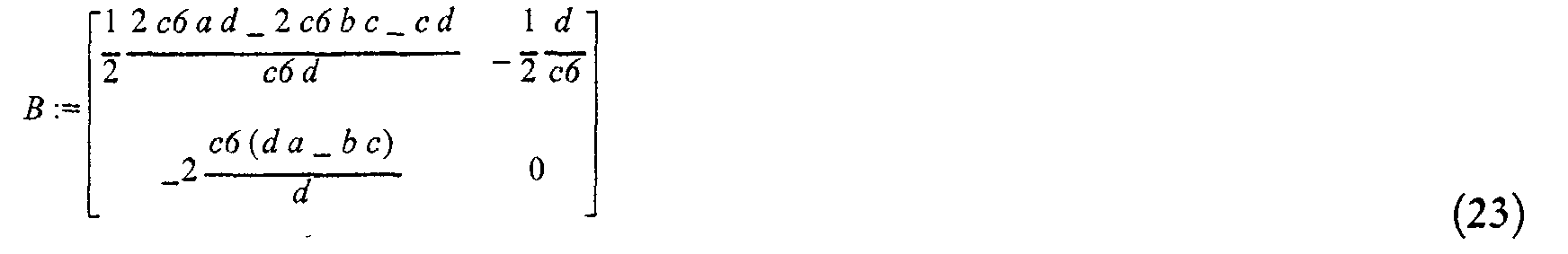
The ray Ya in the object point yob with the desired angle ya is given by the vector:and the distance l between the object and the first mirror surface by the matrix: The first mirror surface is given by:
 The distance m between the first mirror and the second mirror is given by:
 The unknown matrix from the second mirror surface to the stop position is defined as
 The chief ray in the stop surface is now:
 and in the image the chief ray is:
 The height of the chief ray in the image is by definition magn *height in the object surface (yob), we solve I from equation (30) to impose this reduction to the system giving:
 And as a check we calculate the chief ray after the 6th surface with the new expressions. We see that the angle is always zero and that the height is the object height multiplied with magnification.
 The final solve is the distance n between the last mirror surface and the image surface. In the image surface all rays from the same object point come together in a point with a height = magnification *object height.
- First we define a ray Yb from the object point yob and an arbitrary angle yb.
 In the image this ray Yb will become:
 The expression for the image distance n is, given that the image height is equal to magn.yob:
- Now we use these derivations in the first part: solving the variables of a six-mirror system with the stop position on mirror two, defining thicknesses as d: =[d0,d1,d2,d3,d4,d5,d6] and the curvatures as c:=[c1,c2,c3,c4,c5,c6]. The stop (pupil) position is on the second surface.
- A limitation on the Petzval sum (i.e. the sum of curvatures in the system, curvatures of odd surfaces being subtracted from curvatures of even surfaces, or vice versa), e.g. to be zero, can be introduced and used to solve the curvature of the stop surface. However, a zero Petzval sum is not essential and an non-zero value can be accommodated.
- Now we define all the matrices in the system, the reflectance (even subscripts) and translation (odd subscripts) matrices, from the object to the image.

- The first solve is the exit pupil in infinity or telecentricity in the image. The angle of the ray going through the optical axis in the stop surface should be zero in the image. The matrix from the stop surface to the fifth mirror generated by multiplication of the appropriate M matrices derived just above, is given by:So as we derived the distance between mirror 5 and 6, we solve this new found value in the appropriate matrix and the vector of distances.
 and the distance between the object and the first mirror is:
- The original derivations can similarly be used to solve the variables of a six-mirror system with the stop position on mirror three, as will now be shown.
- The first solve is pupil in infinity or telecentricity in the image. The angle of the ray going through the optical axis in the stop surface should be zero in the image. The matrix from the stop surface to the fifth mirror generated by multiplication of the appropriate M matrices derived just above, is given by:The matrix from the second mirror surface to the stop surface is given by:
 So, as derived above, the distance between mirror 5 and 6 is, solved this new found value in the appropriate matrix and the vector of distances:
 The distance between mirror one and two was:
- Similarly, the original derivations can be used to solve the variables of a six-mirror system with the stop position on mirror four.
- Again, the first solve is pupil in infinity or telecentricity in the image. The angle of the ray going through the optical axis in the stop surface should be zero in the image. The matrix from the stop surface to the fifth mirror generated by multiplication of the appropriate M matrices derived above is given by:The matrix from the second mirror surface to the stop surface is given by:
 So, as derived above, the distance between mirror 5 and 6, solved in the appropriate matrix and the vector of distances, is:
- Again, we use the original derivations to solve the variables of a six-mirror system with the stop position on mirror five. As before, the first solve is pupil in infinity or telecentricity in the image. The angle of the ray going through the optical axis in the stop surface should be zero in the image. The matrix from the stop surface to the fifth mirror generated by multiplication of the appropriate M matrices derived above is given by:The matrix from the second mirror surface to the stop surface is given by:

- Yet again, we can use these derivations to solve the variables of a four-mirror system with the stop position on mirror two. As usual, the first solve is pupil in infinity or telecentricity in the image. The angle of the ray going through the optical axis in the stop surface should be zero in the image. The matrix from the stop surface to the third mirror generated by multiplication of the appropriate M matrices derived above, is given by:The matrix from the second mirror surface to the stop surface is given by:
 So as derived above, the distance between
mirror - Again, we use the original derivations to solve the variables of a four-mirror system with the stop position on mirror three. The first solve is pupil in infinity or telecentricity in the image.
The angle of the ray going through the optical axis in the stop surface should be zero in the image. The matrix from the stop surface to the third mirror generated by multiplication of the appropriate M matrices derived above is given by:The matrix from the second mirror surface to the stop surface is given by: So as we derived the distance between
mirror And the distance between the object and the first mirror:
- A particular problem in designing mirror systems, not encountered in refractive lens systems, is ensuring that the beam is not obscured in its zigzag course by other mirrors. Because of the necessary zigzag path, as the projection beam proceeds between successive mirrors I and I+1 on the optical path in many cases it will pass by at least one other mirror J. Thus, for an optical system not to be obscured it is necessary to ensure that the position and extent of the intervening mirror J is such that it does not intersect any part of the beam between mirrors I and I+1. This is shown in Figure 4 in which it can be seen that mirror J lies wholly below the beam between I and I+1 whereas mirror J' partially intersects the beam. The arrangement of mirror J is not permitted.
- In a model of a potential projection system, obscuration can be detected by the following procedure:
- 1. For each pair of successive mirrors I, I+1 on the optical path, check if there exists a mirror J (with J not equal to I, I+1) having a position on the optical axis (Z axis) between I and I+1
- 2. If J exists, calculate the distance from the optical axis (Y position) of the extreme rays from I to I+1 at the position of mirror J on the optical axis.
- 3. Check that the top and bottom of mirror J are both above (i.e. have greater Y position) or both below (i.e. have smaller Y position) both the extreme rays from I to I+1. If the check in (3) fails, then mirror J at least partially obscures the beam from I to
-
- Figure 6 shows a mirror system in class 9(+) which can be used in the lithography apparatus of Figure 1. In this class, the stop can be positioned on
mirror 2 or 3; in the system of Figure 6, the stop position is on surface 2. The ring field of this system is defined on the object side, between 114 and 118 arbitrary units, with a numerical aperture of 0.25 (0.05 on the object side). The magnification is 0.2 and an intermediate image is formed betweenmirrors - Figure 7 also shows a mirror system in class 9(+). In this case the stop is on
mirror 3 and the intermediate image is betweenmirrors 1 and 2. The first order curvatures and thicknesses of this system, in arbitrary units, are given in Table 2 below. - Figure 8 shows an example of a class 2(-) system having the stop located on the third mirror. From the object (mask MA, surface 0) all the rays go, with a negative angle (a zero angle is parallel to the optical axis), to the first convex mirror M1. The convex mirror M1 reflects the beam upward to a large concave mirror M2. The position of the second mirror M2 has to be above the beam between the object (mask MA) and mirror M1. The beam then goes under mirror M1 to the stop surface mirror M3. From the stop surface the beam is reflected to concave mirror M4. Mirror M4 takes care of a telecentric illumination of the image (surface 5). The first order curvatures and thicknesses of this system, in arbitrary units, are given in Table 3 below.
- A class 6(-) system, shown in Figure 9, consists of two mirror pairs, in a symmetrical design. From the object (mask MA, surface 0) all the rays go, with a negative angle (a zero angle is parallel to the optical axis), to the first convex mirror M1. The object is illuminated as telecentric as possible, this being a requirement for lithography. The convex mirror M1 reflects the beam upward to a large concave mirror M2. The position of this mirror has to be above the beam between the object and mirror M1. So far this design resembles the class 2(-) design (shown in Figure 8). The beam then goes over mirror M1 to the stop surface on mirror M3, limited by the top of mirror M1. From the stop surface M3 the beam is reflected to concave mirror M4. Mirror M4 takes care of a telecentric illumination of the image (surface 5). The ring field of this system is defined on the image side, between -22.8 and -23.8, resulting in a Strehl ratio of at least 0.972 with a numerical aperture of 0.15. The first order curvatures and thicknesses of this system, in arbitrary units, are given in Table 4 below.
- A class 9(-) system with a stop on the second surface is shown in Figure 10. The ring field of this system is defined on the object side, between 114 and 118 arbitrary units, with a numerical aperture of 0.2 (0.05 on the object side). The first order curvatures and thicknesses of this system, in arbitrary units, are given in Table 5 below.
- Figure 11 shows a system in class 10(-). The ring field of this system is defined on the object side, between 114 and 118 arbitrary units, with a numerical aperture of 0.2 (0.05 on the object side). The first order curvatures and thicknesses of this system, in arbitrary units, are given in Table 6 below.
- All the six-mirror systems found to be feasible have, as they have a positive magnification, an intermediate image.
- Figure 12 shows a six-mirror system in class 9(+) in which the stop can be positioned on
mirror - A class 37(+) six-mirror system can have the stop positioned on
mirror - The system shown in Figure 13 has the stop on surface 2. This system consists of a mirror pair near the object and four-mirrors grouped near the image. From the object (mask MA, surface 0) all the rays go, with a negative angle, to the first concave mirror M1. The concave mirror M1 reflects the beam downward to mirror M2 which is almost flat. The top of mirror M2 is restricted to be below the beam between the object and mirror M1. The beam between mirror M2 and M3 limits the bottom of the small mirror M4, whilst the beam between mirror M4 and M5 limits the top of mirror M4. Finally, the beam between the last mirror M6 and the image limits the top of mirror M5. The first order curvatures and thicknesses of this system, in arbitrary units, are given in Table 8 below.
- For comparison, Figure 14 shows a class 37(+) six-mirror system with the stop on surface 5. The ring field of this system is defined on the image side, between 27 and 30 arbitrary units, with a numerical aperture of 0.24. The first order curvatures and thicknesses of this system, in arbitrary units, are given in Table 9 below.
- An eight-mirror system in class 165(+) with stop on
surface 3 is shown in Figure 15. The ring field of this system is defined on the object side, between 116 and 124 arbitrary units, with a numerical aperture of 0.24 (0.06 on the object side). The first order curvatures and thicknesses of this system, in arbitrary units, are given in Table 10 below. - An eight mirror system in class 169(+) is shown in Figure 16, the curvatures and thicknesses of its elements are shown in Table 11. This system has a ring field in the object side between 114 and 118 arbitrary units, a numerical aperture of 0.4, distortion <2.9 nm and an rms wavefront error <0.3λ.
- An eight mirror system in class 181(+) is shown in Figure 17, the curvatures and thicknesses of its elements are shown in Table 12. Again, the ring field on the object side is between 114 and 118 units and the numerical aperture is 0.4. However, the distortion is < 1.9 nm and the rms wavefront error <0.5λ.
- An eight mirror system in class 150(-) is shown in Figure 18, the curvatures and thicknesses of its elements are shown in Table 13. This system provides a distortion <2.6 nm and an rms wavefront error <0.19λ.
- An eight mirror system in class 182(-) is shown in Figure 19, the curvatures and thicknesses of its elements are shown in Table 14. This system likewise has a ring field on the object side between 114 and 118 arbitrary units, a numerical aperture of 0.4, an rms wavefront error of <1λ and a distortion <2.18 nm.
- Whilst we have described above specific embodiments of the invention it will be appreciated that the invention may be practiced otherwise than described. The description is not intended to limit the invention.


Claims (15)
- A lithographic projection apparatus comprising:characterized in that:a radiation system for providing a projection beam of radiation;a support structure for supporting patterning means, the patterning means serving to pattern the projection beam according to a desired pattern;a substrate table for holding a substrate;a projection system for projecting the patterned beam onto a target portion of the substrate,said projection system has precisely four imaging mirrors in the optical path of the projection beam and has an incidence angle classification, C, of 2(-), 6(-), or 9(-), where:
 ai = 1 if the angle of incidence of the chief ray at mirror i is negative,ai = 0 if the angle of incidence of the chief ray at mirror i is positive,M is the magnification of the projection system, andthe index i numbers the mirrors from object to image.
 - Apparatus according to claim 1 wherein said projection system has a stop on the second or third mirror.
- Apparatus according to claim 1 or 2 wherein said projection system has an intermediate image between the first and second mirrors, between the second and third or between the third and fourth mirrors.
- A lithographic projection apparatus comprising:characterized in that:a radiation system for providing a projection beam of radiation;a support structure for supporting patterning means, the patterning means serving to pattern the projection beam according to a desired pattern;a substrate table for holding a substrate;a projection system for projecting the patterned beam onto a target portion of the substrate,said projection system has precisely six imaging mirrors in the optical path of the projection beam and has an incidence angle classification, C, of 5(+), 6(-), 9(+), 13(+), 18(-), 21(+), 22(-), 25(+), 29(+), 34(-), 37(+), 38(-), 42(-), or 54(-), where:
 ai = 1 if the angle of incidence of the chief ray at mirror i is negative,ai = 0 if the angle of incidence of the chief ray at mirror i is positive,M is the magnification of the projection system, andthe index i numbers the mirrors from object to image.
 - Apparatus according to claim 5, wherein said projection system has a stop located on the second, third, fourth or fifth mirror.
- Apparatus according to claim 4 or 5, wherein said projection system has an intermediate image between the second and fifth mirror.
- A lithographic projection apparatus comprising:characterized in that:a radiation system for providing a projection beam of radiation;a support structure for supporting patterning means, the patterning means serving to pattern the projection beam according to a desired pattern;a substrate table for holding a substrate;a projection system for projecting the patterned beam onto a target portion of the substrate,said projection system has precisely eight imaging mirrors in the optical path of the projection beam and has an incidence angle classification, C, of 2(+), 5(+), 9(+), 12(+), 13(+), 18(+), 18(-), 19(+), 20(+), 21(+), 22(+), 23(+), 25(+), 26(+), 34(-), 36(+), 37(+), 38(-), 45(+), 46(+), 49(+), 52(+), 53(+), 54(+), 54(-), 55(-), 58(-), 68(+), 69(+), 73(+), 74(+) 77(+), 82(+), 82(-), 85(+), 88(+), 89(+), 90(-), 92(+), 93(+), 97(+), 100(-), 101(+), 102(-), 104(+), 105(+), 106(+), 106(-), 107(+), 108(+), 109(+), 109(-), 110(+), 110(-), 111(+), 113(+), 116(+), 117(+), 118(+), 118(-), 120(+), 121(+), 122(-), 123(-), 132(+), 133(+), 134(-), 137(+), 138(+), 141(+), 145(+), 145(-), 146(+), 146(-), 147(+), 148(+), 148(-), 149(+), 150(+), 150(-), 151(+), 151(-), 152(-), 153(+), 154(+), 154(-), 155(+), 155(-), 156(+), 157(+), 159(+), 161(+), 162(-), 163(-), 164(+), 165(+), 166(+), 166(-), 167(+), 168(+), 169(+), 170(+), 170(-), 171(+), 172(+), 173(+), 174(+), 175(+), 176(+), 177(+), 178(-), 179(+), 180(+), 180(-), 181(+), 181(-), 182(+), 182(-), 183(+), 183(-), 184(+), 185(+), 185(-), 186(-), 187(+), 187(-), 188(-), 189(+), 196(+), 197(+), 201(+), 203(+), 205(+), 209(+), 214(-), 216(+), 217(+), 218(+), 218(-), 225(+), 228(+), 229(+), 230(+), 232(+), 233(+), 235(+), 236(+), 237(+), 238(-), 243(+), 246(+), 247(+), 248(+), 250(-), where:
 ai = 1 if the angle of incidence of the chief ray at mirror i is negative,ai = 0 if the angle of incidence of the chief ray at mirror i is positive,M is the magnification of the projection system, andthe index i numbers the mirrors from object to image.
 - Apparatus according to any one of the preceding claims wherein said projection system has the smallest deviation from telecentricity whilst still enabling obscuration-free illumination of the mask such that, for each point on the object, in the pencil of rays leaving the object, the ray forming the smallest angle with the optical axis forms an angle not larger than 10° to the optical axis.
- Apparatus according to any one of the preceding claims wherein said projection is substantially telecentric on the image side such that for each point on the object, the ray passing through the center of the aperture stop forms in the image space an angle with the optical axis not larger than 1°.
- Apparatus according to any one of the preceding claims wherein each mirror in said projection system is substantially rotationally symmetric about an optical axis.
- Apparatus according to any one of the preceding claims wherein said projection system has a magnification whose absolute value is in the range of from 1/3 to 1/10 and preferably substantially equal to 1/4 or 1/5.
- Apparatus according to any one of the preceding claims wherein said projection beam comprises extreme ultraviolet radiation, e.g. having a wavelength in the range of from 8 to 20nm, preferably 9 to 16nm.
- An apparatus according to any one of the preceding claims, wherein the support structure comprises a mask table for holding a mask.
- An apparatus according to any one of the preceding claims, wherein the radiation system comprises a radiation source.
- A device manufacturing method comprising the steps of:characterized in that:providing a substrate that is at least partially covered by a layer of radiation-sensitive material;providing a projection beam of radiation using a radiation system;using patterning means to endow the projection beam with a pattern in its cross-section;projecting the patterned beam of radiation onto a target portion of the layer of radiation-sensitive material;in the step of imaging, a projection system as defined in any one of the preceding claims is used.
Priority Applications (4)
| Application Number | Priority Date | Filing Date | Title |
|---|---|---|---|
| EP09158673A EP2081086B1 (en) | 2000-11-07 | 2001-11-05 | Lithographic apparatus and device manufacturing method |
| EP20010309353 EP1209503B1 (en) | 2000-11-07 | 2001-11-05 | Lithographic apparatus and device manufacturing method |
| EP06004926A EP1679550A1 (en) | 2000-11-07 | 2001-11-05 | Lithographic apparatus and device manufacturing method |
| EP06004927A EP1679551A1 (en) | 2000-11-07 | 2001-11-05 | Lithographic apparatus and device manufacturing method |
Applications Claiming Priority (3)
| Application Number | Priority Date | Filing Date | Title |
|---|---|---|---|
| EP00309871 | 2000-11-07 | ||
| EP00309871 | 2000-11-07 | ||
| EP20010309353 EP1209503B1 (en) | 2000-11-07 | 2001-11-05 | Lithographic apparatus and device manufacturing method |
Related Child Applications (2)
| Application Number | Title | Priority Date | Filing Date |
|---|---|---|---|
| EP06004927A Division EP1679551A1 (en) | 2000-11-07 | 2001-11-05 | Lithographic apparatus and device manufacturing method |
| EP06004926A Division EP1679550A1 (en) | 2000-11-07 | 2001-11-05 | Lithographic apparatus and device manufacturing method |
Publications (3)
| Publication Number | Publication Date |
|---|---|
| EP1209503A2 true EP1209503A2 (en) | 2002-05-29 |
| EP1209503A3 EP1209503A3 (en) | 2004-07-28 |
| EP1209503B1 EP1209503B1 (en) | 2009-01-07 |
Family
ID=26073355
Family Applications (4)
| Application Number | Title | Priority Date | Filing Date |
|---|---|---|---|
| EP06004927A Ceased EP1679551A1 (en) | 2000-11-07 | 2001-11-05 | Lithographic apparatus and device manufacturing method |
| EP20010309353 Expired - Lifetime EP1209503B1 (en) | 2000-11-07 | 2001-11-05 | Lithographic apparatus and device manufacturing method |
| EP09158673A Expired - Lifetime EP2081086B1 (en) | 2000-11-07 | 2001-11-05 | Lithographic apparatus and device manufacturing method |
| EP06004926A Ceased EP1679550A1 (en) | 2000-11-07 | 2001-11-05 | Lithographic apparatus and device manufacturing method |
Family Applications Before (1)
| Application Number | Title | Priority Date | Filing Date |
|---|---|---|---|
| EP06004927A Ceased EP1679551A1 (en) | 2000-11-07 | 2001-11-05 | Lithographic apparatus and device manufacturing method |
Family Applications After (2)
| Application Number | Title | Priority Date | Filing Date |
|---|---|---|---|
| EP09158673A Expired - Lifetime EP2081086B1 (en) | 2000-11-07 | 2001-11-05 | Lithographic apparatus and device manufacturing method |
| EP06004926A Ceased EP1679550A1 (en) | 2000-11-07 | 2001-11-05 | Lithographic apparatus and device manufacturing method |
Country Status (1)
| Country | Link |
|---|---|
| EP (4) | EP1679551A1 (en) |
Cited By (10)
| Publication number | Priority date | Publication date | Assignee | Title |
|---|---|---|---|---|
| WO2004010224A2 (en) * | 2002-07-22 | 2004-01-29 | Carl Zeiss Smt Ag | Projection objective for a projection exposure apparatus |
| EP1434093A2 (en) * | 2002-12-27 | 2004-06-30 | Canon Kabushiki Kaisha | Catoptric projection system, exposure apparatus and device fabrication method |
| EP1450209A1 (en) * | 2003-02-21 | 2004-08-25 | Canon Kabushiki Kaisha | Catoptric projection optical system |
| US7126671B2 (en) | 2003-04-04 | 2006-10-24 | Asml Netherlands B.V. | Lithographic apparatus and device manufacturing method |
| WO2006117122A1 (en) * | 2005-05-03 | 2006-11-09 | Carl Zeiss Smt Ag | Microlithography exposure apparatus using polarized light and microlithography projection system having concave primary and secondary mirrors |
| US7186983B2 (en) | 1998-05-05 | 2007-03-06 | Carl Zeiss Smt Ag | Illumination system particularly for microlithography |
| US7592598B2 (en) | 1998-05-05 | 2009-09-22 | Carl Zeiss Smt Ag | Illumination system particularly for microlithography |
| EP2169465A1 (en) * | 2005-05-13 | 2010-03-31 | Carl Zeiss SMT AG | A six-mirror EUV projection system |
| WO2010099899A1 (en) * | 2009-03-06 | 2010-09-10 | Carl Zeiss Smt Ag | Imaging optics and projection exposure installation for microlithography with an imaging optics of this type |
| WO2010115500A1 (en) * | 2009-03-30 | 2010-10-14 | Carl Zeiss Smt Ag | Imaging optics and projection exposure installation for microlithography with an imaging optics of this type |
Families Citing this family (1)
| Publication number | Priority date | Publication date | Assignee | Title |
|---|---|---|---|---|
| TWI266959B (en) | 2001-06-20 | 2006-11-21 | Asml Netherlands Bv | Device manufacturing method, device manufactured thereby and a mask for use in the method |
Citations (7)
| Publication number | Priority date | Publication date | Assignee | Title |
|---|---|---|---|---|
| EP0779528A2 (en) * | 1995-12-12 | 1997-06-18 | Svg Lithography Systems, Inc. | High numerical aperture ring field optical reduction system |
| US5686728A (en) * | 1996-05-01 | 1997-11-11 | Lucent Technologies Inc | Projection lithography system and method using all-reflective optical elements |
| EP0962830A1 (en) * | 1998-05-30 | 1999-12-08 | Carl Zeiss | Ringfield four mirror system with convex primary mirror for EUV lithography |
| US6172825B1 (en) * | 1998-09-22 | 2001-01-09 | Nikon Corporation | Catoptric reduction projection optical system and projection exposure apparatus and method using same |
| EP1093021A2 (en) * | 1999-10-15 | 2001-04-18 | Nikon Corporation | Projection optical system as well as equipment and methods making use of said system |
| US20010002155A1 (en) * | 1998-09-21 | 2001-05-31 | Nikon Corporation | Catoptric reduction projection optical system and exposure apparatus and method using same |
| EP1199590A1 (en) * | 2000-10-20 | 2002-04-24 | Carl Zeiss | 8 mirror microlithography projection lens |
Family Cites Families (9)
| Publication number | Priority date | Publication date | Assignee | Title |
|---|---|---|---|---|
| US5523193A (en) | 1988-05-31 | 1996-06-04 | Texas Instruments Incorporated | Method and apparatus for patterning and imaging member |
| ATE123885T1 (en) | 1990-05-02 | 1995-06-15 | Fraunhofer Ges Forschung | EXPOSURE DEVICE. |
| US5229872A (en) | 1992-01-21 | 1993-07-20 | Hughes Aircraft Company | Exposure device including an electrically aligned electronic mask for micropatterning |
| JP4075966B2 (en) | 1996-03-06 | 2008-04-16 | エーエスエムエル ネザーランズ ビー.ブイ. | Differential interferometer system and lithographic step-and-scan apparatus comprising this system |
| KR100512450B1 (en) | 1996-12-24 | 2006-01-27 | 에이에스엠엘 네델란즈 비.브이. | Two-dimensionally stabilized positioning device with two object holders and lithographic device with such positioning device |
| JP3626504B2 (en) | 1997-03-10 | 2005-03-09 | アーエスエム リソグラフィ ベスローテン フェンノートシャップ | Positioning device having two article holders |
| US6396067B1 (en) | 1998-05-06 | 2002-05-28 | Koninklijke Philips Electronics N.V. | Mirror projection system for a scanning lithographic projection apparatus, and lithographic apparatus comprising such a system |
| US6255661B1 (en) | 1998-05-06 | 2001-07-03 | U.S. Philips Corporation | Mirror projection system for a scanning lithographic projection apparatus, and lithographic apparatus comprising such a system |
| JP2000098230A (en) * | 1998-09-22 | 2000-04-07 | Nikon Corp | Reflecting reduction image-forming optical system, aligner equipped therewith and exposing method using the same optical system |
-
2001
- 2001-11-05 EP EP06004927A patent/EP1679551A1/en not_active Ceased
- 2001-11-05 EP EP20010309353 patent/EP1209503B1/en not_active Expired - Lifetime
- 2001-11-05 EP EP09158673A patent/EP2081086B1/en not_active Expired - Lifetime
- 2001-11-05 EP EP06004926A patent/EP1679550A1/en not_active Ceased
Patent Citations (7)
| Publication number | Priority date | Publication date | Assignee | Title |
|---|---|---|---|---|
| EP0779528A2 (en) * | 1995-12-12 | 1997-06-18 | Svg Lithography Systems, Inc. | High numerical aperture ring field optical reduction system |
| US5686728A (en) * | 1996-05-01 | 1997-11-11 | Lucent Technologies Inc | Projection lithography system and method using all-reflective optical elements |
| EP0962830A1 (en) * | 1998-05-30 | 1999-12-08 | Carl Zeiss | Ringfield four mirror system with convex primary mirror for EUV lithography |
| US20010002155A1 (en) * | 1998-09-21 | 2001-05-31 | Nikon Corporation | Catoptric reduction projection optical system and exposure apparatus and method using same |
| US6172825B1 (en) * | 1998-09-22 | 2001-01-09 | Nikon Corporation | Catoptric reduction projection optical system and projection exposure apparatus and method using same |
| EP1093021A2 (en) * | 1999-10-15 | 2001-04-18 | Nikon Corporation | Projection optical system as well as equipment and methods making use of said system |
| EP1199590A1 (en) * | 2000-10-20 | 2002-04-24 | Carl Zeiss | 8 mirror microlithography projection lens |
Non-Patent Citations (1)
| Title |
|---|
| LERNER S A ET AL: "DESIGN APPROACH AND COMPARISON OF PROJECTION CAMERAS FOR EUV LITHOGRAPHY" OPTICAL ENGINEERING, SOC. OF PHOTO-OPTICAL INSTRUMENTATION ENGINEERS. BELLINGHAM, US, vol. 39, no. 3, March 2000 (2000-03), pages 792-802, XP001051258 ISSN: 0091-3286 * |
Cited By (21)
| Publication number | Priority date | Publication date | Assignee | Title |
|---|---|---|---|---|
| US7186983B2 (en) | 1998-05-05 | 2007-03-06 | Carl Zeiss Smt Ag | Illumination system particularly for microlithography |
| US7977651B2 (en) | 1998-05-05 | 2011-07-12 | Carl Zeiss Smt Gmbh | Illumination system particularly for microlithography |
| US7592598B2 (en) | 1998-05-05 | 2009-09-22 | Carl Zeiss Smt Ag | Illumination system particularly for microlithography |
| US7456408B2 (en) | 1998-05-05 | 2008-11-25 | Carl Zeiss Smt Ag | Illumination system particularly for microlithography |
| US7348565B2 (en) | 1998-05-05 | 2008-03-25 | Carl Zeiss Smt Ag | Illumination system particularly for microlithography |
| WO2004010224A3 (en) * | 2002-07-22 | 2004-07-29 | Zeiss Carl Smt Ag | Projection objective for a projection exposure apparatus |
| WO2004010224A2 (en) * | 2002-07-22 | 2004-01-29 | Carl Zeiss Smt Ag | Projection objective for a projection exposure apparatus |
| EP1434093A3 (en) * | 2002-12-27 | 2006-08-02 | Canon Kabushiki Kaisha | Catoptric projection system, exposure apparatus and device fabrication method |
| EP1434093A2 (en) * | 2002-12-27 | 2004-06-30 | Canon Kabushiki Kaisha | Catoptric projection system, exposure apparatus and device fabrication method |
| US7070289B2 (en) | 2003-02-21 | 2006-07-04 | Canon Kabushiki Kaisha | Catoptric projection optical system |
| EP1450209A1 (en) * | 2003-02-21 | 2004-08-25 | Canon Kabushiki Kaisha | Catoptric projection optical system |
| US7226177B2 (en) | 2003-02-21 | 2007-06-05 | Canon Kabushiki Kaisha | Catoptric projection optical system |
| US7126671B2 (en) | 2003-04-04 | 2006-10-24 | Asml Netherlands B.V. | Lithographic apparatus and device manufacturing method |
| WO2006117122A1 (en) * | 2005-05-03 | 2006-11-09 | Carl Zeiss Smt Ag | Microlithography exposure apparatus using polarized light and microlithography projection system having concave primary and secondary mirrors |
| EP2169465A1 (en) * | 2005-05-13 | 2010-03-31 | Carl Zeiss SMT AG | A six-mirror EUV projection system |
| US7973908B2 (en) | 2005-05-13 | 2011-07-05 | Carl Zeiss Smt Gmbh | Six-mirror EUV projection system with low incidence angles |
| WO2010099899A1 (en) * | 2009-03-06 | 2010-09-10 | Carl Zeiss Smt Ag | Imaging optics and projection exposure installation for microlithography with an imaging optics of this type |
| KR101388330B1 (en) * | 2009-03-06 | 2014-04-22 | 칼 짜이스 에스엠티 게엠베하 | Imaging optics and projection exposure installation for microlithography with an imaging optics of this type |
| US9639004B2 (en) | 2009-03-06 | 2017-05-02 | Carl Zeiss Smt Gmbh | Imaging optics and projection exposure installation for microlithography with an imaging optics |
| WO2010115500A1 (en) * | 2009-03-30 | 2010-10-14 | Carl Zeiss Smt Ag | Imaging optics and projection exposure installation for microlithography with an imaging optics of this type |
| US9057964B2 (en) | 2009-03-30 | 2015-06-16 | Carl Zeiss Smt Gmbh | Imaging optics and projection exposure installation for microlithography with an imaging optics |
Also Published As
| Publication number | Publication date |
|---|---|
| EP1209503B1 (en) | 2009-01-07 |
| EP2081086B1 (en) | 2013-01-02 |
| EP1679550A1 (en) | 2006-07-12 |
| EP2081086A3 (en) | 2010-03-24 |
| EP1209503A3 (en) | 2004-07-28 |
| EP2081086A2 (en) | 2009-07-22 |
| EP1679551A1 (en) | 2006-07-12 |
Similar Documents
| Publication | Publication Date | Title |
|---|---|---|
| US6556648B1 (en) | Lithographic apparatus, device manufacturing method, and device manufactured thereby | |
| US6887625B2 (en) | Assist features for use in lithographic projection | |
| US7466413B2 (en) | Marker structure, mask pattern, alignment method and lithographic method and apparatus | |
| US7859647B2 (en) | Lithographic apparatus and device manufacturing method | |
| US7130049B2 (en) | Method of measurement, method for providing alignment marks, and device manufacturing method | |
| JP2003233001A (en) | Reflection type projection optical system, exposure device, and method for manufacturing device | |
| EP2506061A1 (en) | Image-forming optical system, exposure apparatus, and device producing method | |
| EP2081086B1 (en) | Lithographic apparatus and device manufacturing method | |
| US9075322B2 (en) | Reflective imaging optical system, exposure apparatus, and method for producing device | |
| US7499149B2 (en) | Holographic mask for lithographic apparatus and device manufacturing method | |
| US8259398B2 (en) | High numerical aperture catadioptric objectives without obscuration and applications thereof | |
| US8743342B2 (en) | Reflective imaging optical system, exposure apparatus, and method for producing device | |
| US7113255B2 (en) | Grating patch arrangement, lithographic apparatus, method of testing, device manufacturing method, and device manufactured thereby | |
| EP1174764B1 (en) | Assist features for use in lithographic projection | |
| Hawryluk et al. | EUV lithography | |
| US7312850B2 (en) | Lithographic apparatus, illumination system, and optical element for rotating an intensity distribution | |
| JP2019168728A (en) | Illumination optical system, exposure equipment, and device manufacturing method | |
| US20070165296A1 (en) | Method of designing a projection system, lithographic apparatus and device manufacturing method | |
| US7244534B2 (en) | Device manufacturing method | |
| EP1498779A2 (en) | Marker structure for alignment or overlay | |
| WO2010052961A1 (en) | Imaging optical system, exposure apparatus and device manufacturing method |
Legal Events
| Date | Code | Title | Description |
|---|---|---|---|
| PUAI | Public reference made under article 153(3) epc to a published international application that has entered the european phase |
Free format text: ORIGINAL CODE: 0009012 |
|
| AK | Designated contracting states |
Kind code of ref document: A2 Designated state(s): AT BE CH CY DE DK ES FI FR GB GR IE IT LI LU MC NL PT SE TR |
|
| AX | Request for extension of the european patent |
Free format text: AL;LT;LV;MK;RO;SI |
|
| RAP1 | Party data changed (applicant data changed or rights of an application transferred) |
Owner name: ASML NETHERLANDS B.V. |
|
| RIC1 | Information provided on ipc code assigned before grant |
Ipc: 7G 03F 7/20 A Ipc: 7G 02B 17/06 B |
|
| PUAL | Search report despatched |
Free format text: ORIGINAL CODE: 0009013 |
|
| AK | Designated contracting states |
Kind code of ref document: A3 Designated state(s): AT BE CH CY DE DK ES FI FR GB GR IE IT LI LU MC NL PT SE TR |
|
| AX | Request for extension of the european patent |
Extension state: AL LT LV MK RO SI |
|
| RAP1 | Party data changed (applicant data changed or rights of an application transferred) |
Owner name: ASML NETHERLANDS B.V. |
|
| 17P | Request for examination filed |
Effective date: 20041130 |
|
| AKX | Designation fees paid |
Designated state(s): DE FR GB IT NL |
|
| 17Q | First examination report despatched |
Effective date: 20050311 |
|
| GRAP | Despatch of communication of intention to grant a patent |
Free format text: ORIGINAL CODE: EPIDOSNIGR1 |
|
| GRAS | Grant fee paid |
Free format text: ORIGINAL CODE: EPIDOSNIGR3 |
|
| GRAA | (expected) grant |
Free format text: ORIGINAL CODE: 0009210 |
|
| AK | Designated contracting states |
Kind code of ref document: B1 Designated state(s): DE FR GB IT NL |
|
| REG | Reference to a national code |
Ref country code: GB Ref legal event code: FG4D |
|
| REF | Corresponds to: |
Ref document number: 60137301 Country of ref document: DE Date of ref document: 20090226 Kind code of ref document: P |
|
| PG25 | Lapsed in a contracting state [announced via postgrant information from national office to epo] |
Ref country code: NL Free format text: LAPSE BECAUSE OF FAILURE TO SUBMIT A TRANSLATION OF THE DESCRIPTION OR TO PAY THE FEE WITHIN THE PRESCRIBED TIME-LIMIT Effective date: 20090107 |
|
| NLV1 | Nl: lapsed or annulled due to failure to fulfill the requirements of art. 29p and 29m of the patents act | ||
| PLBE | No opposition filed within time limit |
Free format text: ORIGINAL CODE: 0009261 |
|
| STAA | Information on the status of an ep patent application or granted ep patent |
Free format text: STATUS: NO OPPOSITION FILED WITHIN TIME LIMIT |
|
| 26N | No opposition filed |
Effective date: 20091008 |
|
| GBPC | Gb: european patent ceased through non-payment of renewal fee |
Effective date: 20091105 |
|
| PG25 | Lapsed in a contracting state [announced via postgrant information from national office to epo] |
Ref country code: GB Free format text: LAPSE BECAUSE OF NON-PAYMENT OF DUE FEES Effective date: 20091105 |
|
| PG25 | Lapsed in a contracting state [announced via postgrant information from national office to epo] |
Ref country code: IT Free format text: LAPSE BECAUSE OF FAILURE TO SUBMIT A TRANSLATION OF THE DESCRIPTION OR TO PAY THE FEE WITHIN THE PRESCRIBED TIME-LIMIT Effective date: 20090107 |
|
| REG | Reference to a national code |
Ref country code: FR Ref legal event code: PLFP Year of fee payment: 15 |
|
| REG | Reference to a national code |
Ref country code: FR Ref legal event code: PLFP Year of fee payment: 16 |
|
| REG | Reference to a national code |
Ref country code: FR Ref legal event code: PLFP Year of fee payment: 17 |
|
| PGFP | Annual fee paid to national office [announced via postgrant information from national office to epo] |
Ref country code: DE Payment date: 20171121 Year of fee payment: 17 Ref country code: FR Payment date: 20171121 Year of fee payment: 17 |
|
| REG | Reference to a national code |
Ref country code: DE Ref legal event code: R119 Ref document number: 60137301 Country of ref document: DE |
|
| PG25 | Lapsed in a contracting state [announced via postgrant information from national office to epo] |
Ref country code: FR Free format text: LAPSE BECAUSE OF NON-PAYMENT OF DUE FEES Effective date: 20181130 Ref country code: DE Free format text: LAPSE BECAUSE OF NON-PAYMENT OF DUE FEES Effective date: 20190601 |