EP1218665B1 - Optical element having programmed optical structures - Google Patents
Optical element having programmed optical structures Download PDFInfo
- Publication number
- EP1218665B1 EP1218665B1 EP00973361A EP00973361A EP1218665B1 EP 1218665 B1 EP1218665 B1 EP 1218665B1 EP 00973361 A EP00973361 A EP 00973361A EP 00973361 A EP00973361 A EP 00973361A EP 1218665 B1 EP1218665 B1 EP 1218665B1
- Authority
- EP
- European Patent Office
- Prior art keywords
- optical
- edge
- optical element
- grooves
- lightguide
- Prior art date
- Legal status (The legal status is an assumption and is not a legal conclusion. Google has not performed a legal analysis and makes no representation as to the accuracy of the status listed.)
- Expired - Lifetime
Links
Images

Classifications
-
- G—PHYSICS
- G02—OPTICS
- G02F—OPTICAL DEVICES OR ARRANGEMENTS FOR THE CONTROL OF LIGHT BY MODIFICATION OF THE OPTICAL PROPERTIES OF THE MEDIA OF THE ELEMENTS INVOLVED THEREIN; NON-LINEAR OPTICS; FREQUENCY-CHANGING OF LIGHT; OPTICAL LOGIC ELEMENTS; OPTICAL ANALOGUE/DIGITAL CONVERTERS
- G02F1/00—Devices or arrangements for the control of the intensity, colour, phase, polarisation or direction of light arriving from an independent light source, e.g. switching, gating or modulating; Non-linear optics
- G02F1/01—Devices or arrangements for the control of the intensity, colour, phase, polarisation or direction of light arriving from an independent light source, e.g. switching, gating or modulating; Non-linear optics for the control of the intensity, phase, polarisation or colour
- G02F1/13—Devices or arrangements for the control of the intensity, colour, phase, polarisation or direction of light arriving from an independent light source, e.g. switching, gating or modulating; Non-linear optics for the control of the intensity, phase, polarisation or colour based on liquid crystals, e.g. single liquid crystal display cells
- G02F1/133—Constructional arrangements; Operation of liquid crystal cells; Circuit arrangements
- G02F1/1333—Constructional arrangements; Manufacturing methods
- G02F1/1335—Structural association of cells with optical devices, e.g. polarisers or reflectors
-
- G—PHYSICS
- G02—OPTICS
- G02B—OPTICAL ELEMENTS, SYSTEMS OR APPARATUS
- G02B6/00—Light guides; Structural details of arrangements comprising light guides and other optical elements, e.g. couplings
- G02B6/0001—Light guides; Structural details of arrangements comprising light guides and other optical elements, e.g. couplings specially adapted for lighting devices or systems
- G02B6/0011—Light guides; Structural details of arrangements comprising light guides and other optical elements, e.g. couplings specially adapted for lighting devices or systems the light guides being planar or of plate-like form
- G02B6/0033—Means for improving the coupling-out of light from the light guide
- G02B6/0035—Means for improving the coupling-out of light from the light guide provided on the surface of the light guide or in the bulk of it
- G02B6/0038—Linear indentations or grooves, e.g. arc-shaped grooves or meandering grooves, extending over the full length or width of the light guide
-
- G—PHYSICS
- G02—OPTICS
- G02B—OPTICAL ELEMENTS, SYSTEMS OR APPARATUS
- G02B6/00—Light guides; Structural details of arrangements comprising light guides and other optical elements, e.g. couplings
- G02B6/0001—Light guides; Structural details of arrangements comprising light guides and other optical elements, e.g. couplings specially adapted for lighting devices or systems
- G02B6/0011—Light guides; Structural details of arrangements comprising light guides and other optical elements, e.g. couplings specially adapted for lighting devices or systems the light guides being planar or of plate-like form
- G02B6/0033—Means for improving the coupling-out of light from the light guide
- G02B6/005—Means for improving the coupling-out of light from the light guide provided by one optical element, or plurality thereof, placed on the light output side of the light guide
- G02B6/0051—Diffusing sheet or layer
-
- G—PHYSICS
- G02—OPTICS
- G02B—OPTICAL ELEMENTS, SYSTEMS OR APPARATUS
- G02B6/00—Light guides; Structural details of arrangements comprising light guides and other optical elements, e.g. couplings
- G02B6/0001—Light guides; Structural details of arrangements comprising light guides and other optical elements, e.g. couplings specially adapted for lighting devices or systems
- G02B6/0011—Light guides; Structural details of arrangements comprising light guides and other optical elements, e.g. couplings specially adapted for lighting devices or systems the light guides being planar or of plate-like form
- G02B6/0033—Means for improving the coupling-out of light from the light guide
- G02B6/005—Means for improving the coupling-out of light from the light guide provided by one optical element, or plurality thereof, placed on the light output side of the light guide
- G02B6/0053—Prismatic sheet or layer; Brightness enhancement element, sheet or layer
-
- G—PHYSICS
- G02—OPTICS
- G02F—OPTICAL DEVICES OR ARRANGEMENTS FOR THE CONTROL OF LIGHT BY MODIFICATION OF THE OPTICAL PROPERTIES OF THE MEDIA OF THE ELEMENTS INVOLVED THEREIN; NON-LINEAR OPTICS; FREQUENCY-CHANGING OF LIGHT; OPTICAL LOGIC ELEMENTS; OPTICAL ANALOGUE/DIGITAL CONVERTERS
- G02F1/00—Devices or arrangements for the control of the intensity, colour, phase, polarisation or direction of light arriving from an independent light source, e.g. switching, gating or modulating; Non-linear optics
- G02F1/01—Devices or arrangements for the control of the intensity, colour, phase, polarisation or direction of light arriving from an independent light source, e.g. switching, gating or modulating; Non-linear optics for the control of the intensity, phase, polarisation or colour
- G02F1/13—Devices or arrangements for the control of the intensity, colour, phase, polarisation or direction of light arriving from an independent light source, e.g. switching, gating or modulating; Non-linear optics for the control of the intensity, phase, polarisation or colour based on liquid crystals, e.g. single liquid crystal display cells
- G02F1/133—Constructional arrangements; Operation of liquid crystal cells; Circuit arrangements
- G02F1/1333—Constructional arrangements; Manufacturing methods
- G02F1/1335—Structural association of cells with optical devices, e.g. polarisers or reflectors
- G02F1/1336—Illuminating devices
- G02F1/133615—Edge-illuminating devices, i.e. illuminating from the side
-
- Y—GENERAL TAGGING OF NEW TECHNOLOGICAL DEVELOPMENTS; GENERAL TAGGING OF CROSS-SECTIONAL TECHNOLOGIES SPANNING OVER SEVERAL SECTIONS OF THE IPC; TECHNICAL SUBJECTS COVERED BY FORMER USPC CROSS-REFERENCE ART COLLECTIONS [XRACs] AND DIGESTS
- Y10—TECHNICAL SUBJECTS COVERED BY FORMER USPC
- Y10S—TECHNICAL SUBJECTS COVERED BY FORMER USPC CROSS-REFERENCE ART COLLECTIONS [XRACs] AND DIGESTS
- Y10S385/00—Optical waveguides
- Y10S385/901—Illuminating or display apparatus
Definitions
- the invention relates generally to optical elements and more particularly to lightguides, optical films and other optical elements suitable for use in display devices and having programmed optical structures.
- Backlit display devices such as liquid crystal display (LCD) devices, commonly use a wedge-shaped lightguide.
- the wedge-shaped lightguide couples light from a substantially linear source, such as a cold cathode fluorescent lamp (CCFL), to a substantially planar output.
- CCFL cold cathode fluorescent lamp
- the planar output is then used to illuminate the LCD.
- One measure of the performance of the backlit display is its uniformity. A user can easily perceive relatively small differences in brightness of a display from one area of the display to the next. Even relatively small non-uniformities can be very annoying to a user of the display.
- JP-9145933-A discloses a liquid crystal display device having prismatic projection grooves formed on a prism sheet, which is interposed between a back light unit and a liquid crystal display panel.
- the prism grooves are aligned with gradualty decreasing vertical angles whereby the vertical angle of each prism groove is constant along its groove axis and is different from adjacent prism grooves.
- an optical element such as a lightguide or an optical film, is formed with a predetermined, programmed pattern of optical structures.
- the optical structures may be arranged to selectively correct for non-uniformities in the output of a lightguide, or may be arranged to otherwise effect the performance of the display in a predetermined, and designed manner.
- the present invention is described in terms of several preferred embodiments, and particularly, in terms of an optical film or a lightguide suitable for use in a backlighting system typically used in flat panel display devices, such as a laptop computer display or a desktop flat panel display.
- the invention is not so limited in application and one of ordinary skill in the art will appreciate that it has application to virtually any optical system, for example, to projection screen devices and flat panel televisions. Therefore, the embodiments described herein should not be taken as limiting of the broad scope of the invention.
- an illumination system 10 includes a light source 12; a light source reflector 14; a lightguide 16 with an output surface 18, a back surface 20, an input surface 21 and an end surface 22; a reflector 24 adjacent the back surface 20; a first light redirecting element 26; a second light redirecting element 28; and a reflective polarizer 30.
- the lightguide 16 may be a wedge, a modification thereof or a slab.
- the purpose of the lightguide is to provide for the distribution of light from the light source 12 over an area much larger than the light source 12, and more particulary, substantially over an entire area formed by output surface 18.
- the lightguide 16 further preferably accomplishes these tasks in a compact, thin package.
- the light source 12 may be a CCFL that inputs light to the edge surface 21 of the lightguide 16, and the lamp reflector 14 may be a reflective film that wraps around the light source 12 forming a lamp cavity.
- the reflector 24 backs the lightguide 16 and may be an efficient back reflector, e.g., a lambertian film or a specular film or a combination.
- the edge-coupled light propagates from the input surface 21 toward the end surface 22, confined by total internal reflection (TIR).
- TIR total internal reflection
- the light is extracted from the lightguide 16 by frustration of the TIR.
- a ray confined within the lightguide 16 increases its angle of incidence relative to the plane of the top and bottom walls, due to the wedge angle, with each TIR bounce.
- the light eventually refracts out of the output surface 18 and at a glancing angle thereto, because it is no longer contained by TIR.
- Some of the light rays are extracted out of the back surface 20. These light rays are reflected back into and through the lightguide 16 by the back reflector 24.
- First light redirecting element 26 is arranged as a turning film to redirect these light rays exiting the output surface 18 along a direction substantially parallel to a preferred viewing direction.
- the first light redirecting element 26 may be a light transmissive optical film with an output surface 32 and an input surface 34 formed with prisms (not shown), which refract and reflect the light exiting the lightguide 16 along the preferred viewing direction.
- the prisms may have a substantially uniform configuration, or may have a non-uniform configuration as described in commonly assigned US patent US 6356391 "OPTICAL FILM WITH VARIABLE ANGLE PRISMS" filed of even date herewith.
- the second light redirecting element 28 may not be required in every configuration of the illumination system 10.
- the second light redirecting element may be a diffuser, a lenticular spreader or a prism film, for example a brightness enhancing film such as the.3M Brightness Enhancement Film product (sold as BEFIII) available from Minnesota Mining and Manufacturing Company, St. Paul, Minnesota.
- the reflective polarizer 30 may be an inorganic, polymeric or cholesteric liquid crystal polarizer film.
- a suitable film is the 3M Diffuse Reflective Polarizer Film product (sold as DRPF) or the Specular Reflective Polarizer film product (sold as DBEF), both of which are available from Minnesota Mining and Manufacturing Company.
- at least the second light redirecting element 28 and the reflective polarizer 30, and potentially the first light redirecting element 26, may be combined into a single optical element.
- a diffuser that covers the output surface of the lightguide is typically used.
- a diffuser tends to reduce the overall brightness of the display and may not adequately mask all of the defects.
- the output surface 32 may be formed with optical structures. More particularly, the first light redirecting element 26 has a first edge 36 and a second edge 38. Extending from the first edge 36 toward the second edge 38 are a plurality of optical grooves 40 arranged in a pattern 42. Each groove 40 has formed there an optical structure having characteristic of amplitude, period or aspect ratio of the peaks 44 and valleys 46.
- the pattern 42 may also have characteristics, such as for example, a pitch, p, between grooves 40.
- the grooves 40 in FIG. 2 are shown having amplitude variation. In application of the first light redirecting structure 26, the grooves may be arranged such that variation in amplitude is perpendicular to the lightsource 12.
- the grooves 40 are formed with larger amplitude at the first edge 36 and decrease in amplitude toward the second edge 38.
- the larger amplitude produces more optical power along the groove axis because of the higher surface slopes.
- the optical power of this pattern then decreases as a function of the distance from the first edge 36.
- This arrangement of the grooves 40 and the pattern 42 is purposeful.
- non-uniformities in the output of lightguide 16 may be concentrated near the input surface 21 while there may be less non-uniformity farther from the input surface 21.
- the grooves 40 and the pattern 42 are arranged to provide more diffusion near first edge 36.
- first edge 36 will be disposed substantially adjacent the input surface 21 of the lightguide 16.
- Pattern 42 may have a uniform pitch, p, as shown, and the depth of the grooves 40 may decrease to naught toward the second edge 38. This pattern, as will be discussed in more detail below, may be produced with any tool type.
- the grooves 40 and the pattern 42 may be tailored to correct a particular non-uniformity.
- the grooves 40 and the pattern 42 provided optical power to the output of the lightguide 16 near the input surface 21 in order to mask non-uniformities that may occur near the input surface 21. Less or no optical power is provided away from the input surface 21 as fewer or less intense non-uniformities are typically observed from the lightguide 16 farther from the input surface 21.
- optical power is provided where most needed to mask or soften non-uniformities, while less optical power is provided where there may be fewer non-uniformities to mask.
- optical power may be added virtually anywhere to the output of the lightguide by adding grooves and/or varying the characteristics of the grooves.
- the addition of optical power need not be uniform. Instead, optical power may be added, as necessary, to discrete regions of the lightguide output if necessary to help mask a defect or create a particular optical effect.
- Planar light guides may include an extractor pattern on a back surface of the lightguide.
- the extractor pattern is a pattern of white dots disposed on the back surface of the lightguide. Light incident to one of the dots is diffusely reflected by the white dot, and a portion of this reflected light is caused to exit the light guide.
- the pattern of dots may itself be visible in the lightguide output. Thus, to hide the dot pattern, additional diffusion is typically provided.
- an extractor film 50 which is not part of the present invention is shown.
- a surface 52 of the extractor film are a plurality of optical structures 54 disposed in a pattern 56.
- the optical structures 54 are arranged essentially to replace the white dot pattern for providing extraction of light from the lightguide. While shown in FIG. 3 as circles or dots, the optical structures 54 are not collectively limited to any particular shape nor are they limited to any one particular shape within the pattern 56. Therefore, the optical structures 54 may be prisms, lines, dots, squares, ellipses or generally any shape.
- the optical structures 54 may be spaced very closely together within the pattern 56, much more so than the dots within a dot pattern may be spaced and, for example, within about 50-100 ⁇ m of each other. This very close spacing of the optical structures 54 eliminates or reduces the need for diffusion in the output of the lightguide that is ordinarily necessary to hide the pattern of white dots.
- the invention also permits the changing of the slope of the lightguide at a micro-level. That is, the slope of the lightguide may be locally increased or decreased at the micro-level. When a light ray hits a higher positive slope, it will be extracted from the lightguide faster than if it hit the nominal wedge angle.
- a lightguide 60 has in an input surface 62, and an output surface 64 and a back surface 66.
- the input surface 62 is arranged to be disposed adjacent a light source (not depicted) to provide a source of light incident to the input surface 62.
- the light incident to the input surface 62 is extracted out of the output surface 64 as a result of frustrated TIR within the lightguide 60.
- diffusion is added to the back surface 66 of the lightguide 60 and is further adjusted in intensity extending away from the input surface 62. That is, the back surface 66 is formed with in-phase optical structures 68 arranged to provide diffusive extraction near the input surface 62 and to taper to naught away from the input surface 62.
- the pattern can also be non-tapering, i.e, increasing from naught, randomly varying, or distributed in discrete regions.
- the optical structures can be out-of-phase, such as optical structures 68' formed in a back surface 66' of the lightguide 60' shown in FIG. 6.
- patterns of optical structures may also be formed in the output surface 64 either separately or in conjunction with a pattern formed in the back surface 66.
- the overall purpose of providing the optical structures is to achieve an effect that minimizes non-uniformities of the lightguide output wherever they may occur, and for the lightguide 60 shown in FIGs. 4 and 5, the non-uniformities appear primarily adjacent the input surface 62.
- the optical structures 68 may be formed on a surface 72 of an optical film 70.
- the optical film 70 may then be coupled to the wedge structure of the lightguide 60 using ultraviolet (UV) curing, pressure sensitive or any other suitable adhesive.
- the wedge may be molded in bulk to include the optical structures 68 in the back surface 66.
- optical structures may be formed into an optical film, and the optical film coupled, for example by bonding, to a lightguide or other bulk optical element.
- glare reduction, anti-wetout, Fresnels, and virtually any other structure that may be formed in a surface of an optical film may be easily replicated into the film and then the film coupled to another optical element.
- Films incorporating programmed optical structures may be manufactured using a microreplication process.
- a master is made, for example by cutting the pattern into a metal roll, and the master is used to produce films by extrusion, cast-and-cure, embossing and other suitable processes.
- the films may be compression or injection molded or roll formed.
- a preferred apparatus and method for microreplication is described in the commonly assigned US patent US6322236 entitled "Optical Film With Defect-Reducing Surface and Method of Making Same".
- a linear Fresnel lens or prism 80 has a substantially planar input surface 82 and an output surface 84.
- the output surface 84 is formed with lens structures 86 and superimposed on the lens structures 86 are additional optical structures 88.
- the optical structures 88 have a characteristic of amplitude, period, or aspect ratio, that varies from a first edge 90 of the lens 80 to a second edge 92 of the lens 80.
- the lens 80 may be formed in bulk, or as shown in FIG. 7, the lens structures 86 including the optical structures 88 may be formed on a film 94 that is then bonded to a bulk optical substrate 96.
- the pattern 102 may be formed on a top and/or bottom surface of the film 100. Likewise, the pattern may be formed in a wedge or slab.
- the film 100 has a first edge 104 and a second edge 106. Extending from the first edge 104 toward the second edge.106 are a plurality of grooves 108 arranged in the pattern 102. Each groove 108 has formed thereon an optical structure having a characteristic of amplitude, period or aspect ratio.
- the pattern 102 may also have characteristics, such as for example, a pitch, p, defining a spacing between grooves 108.
- the grooves 108 in FIG. 8 are shown having amplitude variation. In application of the film 100, the grooves may be arranged such that variation in amplitude is perpendicular to a lightsource of the lightguide incorporating the film 100.
- the grooves 108 are formed with larger amplitude at the first edge 104 and decrease in amplitude toward the second edge 106.
- the larger amplitude produces more optical power along the groove axis because of the higher surface slopes.
- the optical power of this pattern then decreases as a function of the distance from the first edge 104.
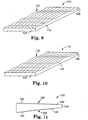
- films 110 and 112 are shown respectively. Each film 110 and 112 has the same characteristics as film 100, and like reference numerals are used to describe like elements therebetween.
- the film 110 FIG. 9, has a pattern 114 of grooves 116 that is formed using a curved nose tool.
- the film 112, FIG. 10, has a pattern 118 of grooves 120 that is formed using a square nose tool.
- the patterns 114 and 118 are arranged as described to provide optical power in the surface or surfaces of the films 110 and 112. It will be appreciated that virtually any tool configuration may be used with the particular tool being selected to achieve a desired amount and form of optical power in the surface or surfaces of the film.
- a first pattern 122 of optical structures 124 is formed in a bottom surface 126 and a second pattern 128 of optical structures 130 is formed in a top surface 132 of the wedge 134.
- the first pattern 122 may be arranged to facilitate the extraction of light from the wedge 134, while the second pattern 128 may be arranged to mask non-uniformities in the light output from the wedge. It will be appreciated, however, that the patterns implemented in the wedge 134 will depend on the desired light output to be achieved from the wedge 134.
- the patterns 122 and 128 may be formed first in an optical film that is later coupled to the wedge, for example, by bonding. In another form, surfaces 122 and 128 are injection molded with the wedge.
Abstract
Description
- The invention relates generally to optical elements and more particularly to lightguides, optical films and other optical elements suitable for use in display devices and having programmed optical structures.
- Backlit display devices, such as liquid crystal display (LCD) devices, commonly use a wedge-shaped lightguide. The wedge-shaped lightguide couples light from a substantially linear source, such as a cold cathode fluorescent lamp (CCFL), to a substantially planar output. The planar output is then used to illuminate the LCD.
- One measure of the performance of the backlit display is its uniformity. A user can easily perceive relatively small differences in brightness of a display from one area of the display to the next. Even relatively small non-uniformities can be very annoying to a user of the display.
- Surface diffusers or bulk diffusers, which scatter the light exiting the lightguide, are sometimes used to mask or soften non-uniformities. However, this diffusion also results in light being directed away from a preferred viewing axis. A net result can be a reduction in overall brightness of the display along the preferred viewing axis, which is another performance measure of a display device.
- Unlike non-uniformities, from a subjective standpoint relatively small increases or decreases in overall brightness are not easily perceived by the user of the display device. However, the display device designer is discouraged by even the smallest decreases in overall brightness including decreases so small they might only be perceived by objective measurement. This is because display brightness and power requirements of the display are closely related. If overall brightness can be increased without increasing the required power, the designer can actually allocate less power to the display device, yet still achieve an acceptable level of brightness. For battery powered portable devices, this translates to longer running times.
- JP-9145933-A discloses a liquid crystal display device having prismatic projection grooves formed on a prism sheet, which is interposed between a back light unit and a liquid crystal display panel. In order to correct any non-uniformities in luminescence in the display, the prism grooves are aligned with gradualty decreasing vertical angles whereby the vertical angle of each prism groove is constant along its groove axis and is different from adjacent prism grooves.
- In accordance with the invention, an optical element, such as a lightguide or an optical film, is formed with a predetermined, programmed pattern of optical structures. The optical structures may be arranged to selectively correct for non-uniformities in the output of a lightguide, or may be arranged to otherwise effect the performance of the display in a predetermined, and designed manner.
- The present invention is defined by the features of claim 1. Preferred embodiments of the present invention are recited in the dependent claims.
- The many advantages and features of the present invention will become apparent to one of ordinary skill in the art from the following detailed description of several preferred embodiments of the invention with reference to the attached drawings wherein like reference numerals refer to like elements throughout and in which:
- Fig. 1 is a perspective view of an illumination device adapted in accordance with an embodiment of the invention;
- FIG. 2 is a perspective view of an optical film incorporating a programmed pattern of optical structures in accordance with one embodiment of the invention;
- FIG. 3 is a perspective view of an optical film incorporating a programmed pattern of optical structures;
- FIG. 4 is a perspective view of a lightguide wedge incorporating an in-phase programmed pattern of optical structures in accordance with another embodiment of the invention;
- FIG. 5 is a cross-section view taken along line 5-5 of in FIG. 4;
- FIG. 6 is a perspective view of a lightguide wedge incorporating an out-of-phase programmed pattern of optical structures in accordance with another embodiment of the invention;
- FIG. 7 is perspective view of a linear lens structure, incorporating a programmed pattern of optical structures in accordance with another embodiment of the invention;
- FIG. 8 is a perspective view of an optical film incorporating a programmed pattern of optical structures in accordances with an alternate preferred embodiment of the invention;
- FIG. 9 is a perspective view of an optical film incorporating a programmed pattern of optical structures in accordances with an alternate preferred embodiment of the invention;
- FIG. 10 is a perspective view of an optical film incorporating a programmed pattern of optical structures in accordances with an alternate preferred embodiment of the invention;
- FIG. 11 is a side view of a lightguide incorporating first programmed pattern of optical structures in a top surface and a second programmed pattern of optical structures in a bottom surface in accordance with a preferred embodiment of the invention.
- The present invention is described in terms of several preferred embodiments, and particularly, in terms of an optical film or a lightguide suitable for use in a backlighting system typically used in flat panel display devices, such as a laptop computer display or a desktop flat panel display. The invention, however, is not so limited in application and one of ordinary skill in the art will appreciate that it has application to virtually any optical system, for example, to projection screen devices and flat panel televisions. Therefore, the embodiments described herein should not be taken as limiting of the broad scope of the invention.
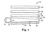
- Referring to Fig. 1, an
illumination system 10 includes alight source 12; alight source reflector 14; alightguide 16 with anoutput surface 18, aback surface 20, aninput surface 21 and anend surface 22; areflector 24 adjacent theback surface 20; a firstlight redirecting element 26; a second light redirecting element 28; and areflective polarizer 30. Thelightguide 16 may be a wedge, a modification thereof or a slab. As is well known, the purpose of the lightguide is to provide for the distribution of light from thelight source 12 over an area much larger than thelight source 12, and more particulary, substantially over an entire area formed byoutput surface 18. Thelightguide 16 further preferably accomplishes these tasks in a compact, thin package. - The
light source 12 may be a CCFL that inputs light to theedge surface 21 of thelightguide 16, and thelamp reflector 14 may be a reflective film that wraps around thelight source 12 forming a lamp cavity. Thereflector 24 backs thelightguide 16 and may be an efficient back reflector, e.g., a lambertian film or a specular film or a combination. - In the embodiment shown, the edge-coupled light propagates from the
input surface 21 toward theend surface 22, confined by total internal reflection (TIR). The light is extracted from thelightguide 16 by frustration of the TIR. A ray confined within thelightguide 16 increases its angle of incidence relative to the plane of the top and bottom walls, due to the wedge angle, with each TIR bounce. Thus, the light eventually refracts out of theoutput surface 18 and at a glancing angle thereto, because it is no longer contained by TIR. Some of the light rays are extracted out of theback surface 20. These light rays are reflected back into and through thelightguide 16 by theback reflector 24. Firstlight redirecting element 26 is arranged as a turning film to redirect these light rays exiting theoutput surface 18 along a direction substantially parallel to a preferred viewing direction. - As shown in Fig. 2, the first
light redirecting element 26 may be a light transmissive optical film with anoutput surface 32 and aninput surface 34 formed with prisms (not shown), which refract and reflect the light exiting thelightguide 16 along the preferred viewing direction. The prisms may have a substantially uniform configuration, or may have a non-uniform configuration as described in commonly assigned US patent US 6356391 "OPTICAL FILM WITH VARIABLE ANGLE PRISMS" filed of even date herewith. - Referring back to FIG. 1, the second light redirecting element 28 may not be required in every configuration of the
illumination system 10. When included in thesystem 10, the second light redirecting element may be a diffuser, a lenticular spreader or a prism film, for example a brightness enhancing film such as the.3M Brightness Enhancement Film product (sold as BEFIII) available from Minnesota Mining and Manufacturing Company, St. Paul, Minnesota. Thereflective polarizer 30 may be an inorganic, polymeric or cholesteric liquid crystal polarizer film. A suitable film is the 3M Diffuse Reflective Polarizer Film product (sold as DRPF) or the Specular Reflective Polarizer film product (sold as DBEF), both of which are available from Minnesota Mining and Manufacturing Company.
Furthermore, at least the second light redirecting element 28 and thereflective polarizer 30, and potentially the firstlight redirecting element 26, may be combined into a single optical element. - With lightguides used for backlighting, such as
lightguide 16, it is common for there to be non-uniformities in the light output from the lightguide. These non-uniformities can frequently be concentrated near theinput surface 21. To mask these defects in applications of the lightguide, a diffuser that covers the output surface of the lightguide is typically used. However, a diffuser tends to reduce the overall brightness of the display and may not adequately mask all of the defects. - Referring now to FIG. 2, shown graphically is a film containing an in-phase varying amplitude pattern. The pattern described may be formed on a top or bottom surface of a wedge, on a plano film, or as described below, on a turning film. In that regard, in addition to the prisms formed on the
input surface 34 of the firstlight redirecting element 26, theoutput surface 32 may be formed with optical structures. More particularly, the firstlight redirecting element 26 has afirst edge 36 and asecond edge 38. Extending from thefirst edge 36 toward thesecond edge 38 are a plurality ofoptical grooves 40 arranged in apattern 42. Eachgroove 40 has formed there an optical structure having characteristic of amplitude, period or aspect ratio of thepeaks 44 andvalleys 46. Thepattern 42 may also have characteristics, such as for example, a pitch, p, betweengrooves 40. Thegrooves 40 in FIG. 2 are shown having amplitude variation. In application of the firstlight redirecting structure 26, the grooves may be arranged such that variation in amplitude is perpendicular to thelightsource 12. - With continued reference to FIG. 2, it is observed that within the
pattern 42, thegrooves 40 are formed with larger amplitude at thefirst edge 36 and decrease in amplitude toward thesecond edge 38. The larger amplitude produces more optical power along the groove axis because of the higher surface slopes. The optical power of this pattern then decreases as a function of the distance from thefirst edge 36. This arrangement of thegrooves 40 and thepattern 42 is purposeful. As noted, non-uniformities in the output oflightguide 16 may be concentrated near theinput surface 21 while there may be less non-uniformity farther from theinput surface 21. Thus, thegrooves 40 and thepattern 42 are arranged to provide more diffusion nearfirst edge 36. In application,first edge 36 will be disposed substantially adjacent theinput surface 21 of thelightguide 16.Pattern 42 may have a uniform pitch, p, as shown, and the depth of thegrooves 40 may decrease to naught toward thesecond edge 38. This pattern, as will be discussed in more detail below, may be produced with any tool type. - It should be appreciated that using ray tracing and other analysis techniques, it is possible to determine particular arrangements for the
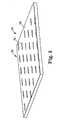
grooves 40 and thepattern 42 that best correct particular observed non-uniformities in the output of thelightguide 16. That is, one or more of the characteristics of thegrooves 40 and thepattern 42 may be tailored to correct a particular non-uniformity. As described above, in connection with firstlight redirecting element 26, thegrooves 40 and thepattern 42 provided optical power to the output of thelightguide 16 near theinput surface 21 in order to mask non-uniformities that may occur near theinput surface 21. Less or no optical power is provided away from theinput surface 21 as fewer or less intense non-uniformities are typically observed from thelightguide 16 farther from theinput surface 21. In this manner, optical power is provided where most needed to mask or soften non-uniformities, while less optical power is provided where there may be fewer non-uniformities to mask. Moreover, optical power may be added virtually anywhere to the output of the lightguide by adding grooves and/or varying the characteristics of the grooves. Furthermore, the addition of optical power need not be uniform. Instead, optical power may be added, as necessary, to discrete regions of the lightguide output if necessary to help mask a defect or create a particular optical effect. - Planar light guides, and some wedge light guides that operate using frustrated TIR, may include an extractor pattern on a back surface of the lightguide. Typically, the extractor pattern is a pattern of white dots disposed on the back surface of the lightguide. Light incident to one of the dots is diffusely reflected by the white dot, and a portion of this reflected light is caused to exit the light guide. In spite of the diffuse nature of this method of extracting light from the lightguide, the pattern of dots may itself be visible in the lightguide output. Thus, to hide the dot pattern, additional diffusion is typically provided.
- With reference to FIG. 3, an
extractor film 50 which is not part of the present invention is shown. Formed in asurface 52 of the extractor film are a plurality ofoptical structures 54 disposed in apattern 56. Theoptical structures 54 are arranged essentially to replace the white dot pattern for providing extraction of light from the lightguide. While shown in FIG. 3 as circles or dots, theoptical structures 54 are not collectively limited to any particular shape nor are they limited to any one particular shape within thepattern 56. Therefore, theoptical structures 54 may be prisms, lines, dots, squares, ellipses or generally any shape. Moreover, theoptical structures 54 may be spaced very closely together within thepattern 56, much more so than the dots within a dot pattern may be spaced and, for example, within about 50-100 µm of each other. This very close spacing of theoptical structures 54 eliminates or reduces the need for diffusion in the output of the lightguide that is ordinarily necessary to hide the pattern of white dots. The invention also permits the changing of the slope of the lightguide at a micro-level. That is, the slope of the lightguide may be locally increased or decreased at the micro-level. When a light ray hits a higher positive slope, it will be extracted from the lightguide faster than if it hit the nominal wedge angle. - While so far discussed in terms of optical films, the invention has application to the lightguide wedge itself. Referring to FIGs. 4 and 5, a
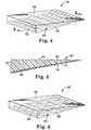
lightguide 60 has in aninput surface 62, and anoutput surface 64 and aback surface 66. Theinput surface 62 is arranged to be disposed adjacent a light source (not depicted) to provide a source of light incident to theinput surface 62. The light incident to theinput surface 62 is extracted out of theoutput surface 64 as a result of frustrated TIR within thelightguide 60. As discussed above, it is common for there to be non-uniformities in the light output from thelightguide 60, particularly near theinput surface 62. - With continued reference to FIGs. 4 and 5, diffusion is added to the
back surface 66 of thelightguide 60 and is further adjusted in intensity extending away from theinput surface 62. That is, theback surface 66 is formed with in-phaseoptical structures 68 arranged to provide diffusive extraction near theinput surface 62 and to taper to naught away from theinput surface 62. The pattern can also be non-tapering, i.e, increasing from naught, randomly varying, or distributed in discrete regions. It is also possible for the optical structures to be out-of-phase, such as optical structures 68' formed in a back surface 66' of the lightguide 60' shown in FIG. 6. It will be appreciated that patterns of optical structures may also be formed in theoutput surface 64 either separately or in conjunction with a pattern formed in theback surface 66. The overall purpose of providing the optical structures is to achieve an effect that minimizes non-uniformities of the lightguide output wherever they may occur, and for thelightguide 60 shown in FIGs. 4 and 5, the non-uniformities appear primarily adjacent theinput surface 62. - With reference to FIG. 5, the
optical structures 68 may be formed on asurface 72 of anoptical film 70. Theoptical film 70 may then be coupled to the wedge structure of thelightguide 60 using ultraviolet (UV) curing, pressure sensitive or any other suitable adhesive. Alternatively, the wedge may be molded in bulk to include theoptical structures 68 in theback surface 66. - As will be more generally appreciated from the foregoing discussion, virtually any configuration of optical structures may be formed into an optical film, and the optical film coupled, for example by bonding, to a lightguide or other bulk optical element. For example, glare reduction, anti-wetout, Fresnels, and virtually any other structure that may be formed in a surface of an optical film may be easily replicated into the film and then the film coupled to another optical element.
- Films incorporating programmed optical structures may be manufactured using a microreplication process. In such a manufacturing process, a master is made, for example by cutting the pattern into a metal roll, and the master is used to produce films by extrusion, cast-and-cure, embossing and other suitable processes. Alternatively, the films may be compression or injection molded or roll formed. A preferred apparatus and method for microreplication is described in the commonly assigned US patent US6322236 entitled "Optical Film With Defect-Reducing Surface and Method of Making Same".
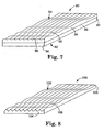
- As an example of the above-described feature of the invention, and with reference to FIG. 7, a linear Fresnel lens or
prism 80 has a substantiallyplanar input surface 82 and anoutput surface 84. Theoutput surface 84 is formed withlens structures 86 and superimposed on thelens structures 86 are additionaloptical structures 88. Theoptical structures 88 have a characteristic of amplitude, period, or aspect ratio, that varies from afirst edge 90 of thelens 80 to asecond edge 92 of thelens 80. Thelens 80 may be formed in bulk, or as shown in FIG. 7, thelens structures 86 including theoptical structures 88 may be formed on afilm 94 that is then bonded to a bulkoptical substrate 96. - Referring now to FIG. 8, shown graphically is a
film 100 containing a varyingamplitude pattern 102 that was formed using a "V" shaped tool. Thepattern 102 may be formed on a top and/or bottom surface of thefilm 100. Likewise, the pattern may be formed in a wedge or slab. Thefilm 100 has afirst edge 104 and asecond edge 106. Extending from thefirst edge 104 toward the second edge.106 are a plurality ofgrooves 108 arranged in thepattern 102. Eachgroove 108 has formed thereon an optical structure having a characteristic of amplitude, period or aspect ratio. Thepattern 102 may also have characteristics, such as for example, a pitch, p, defining a spacing betweengrooves 108. Thegrooves 108 in FIG. 8 are shown having amplitude variation. In application of thefilm 100, the grooves may be arranged such that variation in amplitude is perpendicular to a lightsource of the lightguide incorporating thefilm 100. - With continued reference to FIG. 8, it is observed that within the
pattern 102, thegrooves 108 are formed with larger amplitude at thefirst edge 104 and decrease in amplitude toward thesecond edge 106. The larger amplitude produces more optical power along the groove axis because of the higher surface slopes. The optical power of this pattern then decreases as a function of the distance from thefirst edge 104. This arrangement of thegrooves 108 and thepattern 102 is purposeful. - With reference to FIGs. 9 and 10,
films film film 100, and like reference numerals are used to describe like elements therebetween. As opposed to the pattern created by using a "V" shaped tool, thefilm 110, FIG. 9, has apattern 114 ofgrooves 116 that is formed using a curved nose tool. Thefilm 112, FIG. 10, has apattern 118 ofgrooves 120 that is formed using a square nose tool. Thepatterns films - In the
lightguide 121 illustrated in FIG. 11, afirst pattern 122 ofoptical structures 124 is formed in abottom surface 126 and asecond pattern 128 ofoptical structures 130 is formed in atop surface 132 of thewedge 134. Thefirst pattern 122 may be arranged to facilitate the extraction of light from thewedge 134, while thesecond pattern 128 may be arranged to mask non-uniformities in the light output from the wedge. It will be appreciated, however, that the patterns implemented in thewedge 134 will depend on the desired light output to be achieved from thewedge 134. Moreover, as described above, thepatterns - Still other modifications and alternative embodiments of the invention will be apparent to those skilled in the art in view of the foregoing description. This description is to be construed as illustrative only, and is for the purpose of teaching those skilled in the art the best mode of carrying out the invention. The details of the structure and method may be varied substantially without departing from the invention as defined by the appended claims
Claims (10)
- An optical element having a surface (18, 20), a first edge (36), an opposing second edge (38) and having grooves (40) that are formed in the surface (18, 20) extending from the first edge (36) to the second edge (38), each groove (40) having a groove axis and the groove axes being substantially aligned,
the optical element characterized in that: optical structures having peaks (44) and valleys (46) are formed on each of the grooves (40), and the optical structures provide optical power to the grooves (40), and the optical structures of the peaks (44) and valleys (46) have a characteristic of amplitude, period or aspect ratio that varies along the groove as a function of the location of the optical structure on the groove (40) between the first edge (36) and the second edge (38). - The optical element of claim 1, characterized in that the grooves (40) are prism grooves.
- The optical element of either claim 1 or 2, characterized in that the characteristic comprises amplitude, and wherein the amplitude varies along the groove axis.
- The optical element of either claim 1 or 2, characterized in that the variation in the optical structures of adjacent grooves (40) is one of in-phase and out-of-phase.
- The optical element of either claim 1 or 2, characterized in that the optical power is arranged to be greater along the groove axis at a location arranged to be nearer the first edge (36).
- The optical element of either claim 1 or 2, characterized in that the optical structures comprise discrete optical structures formed in the grooves (40).
- The optical element of either claim 1 or 2, characterized in that the optical structures are continuous structures formed along the length of the groove (40).
- The optical element of either claim 1 or 2, characterized in that the optical - power tapers from a first value to a second, lesser than the first value along the groove axis from a location on the groove axis nearer the first edge (36) to a location on the groove axis nearer the second edge (38).
- The optical element in accordance with any of the preceding claims characterized in that the optical element is one of: a lightguide (16), an optical film (50) and an element of a backlight system (26).
- A method of reducing defects in a light output of a backlight system comprising providing in the backlighting system an optical element in accordance with any of the preceding claims.
Applications Claiming Priority (3)
| Application Number | Priority Date | Filing Date | Title |
|---|---|---|---|
| US09/415,471 US6845212B2 (en) | 1999-10-08 | 1999-10-08 | Optical element having programmed optical structures |
| US415471 | 1999-10-08 | ||
| PCT/US2000/024204 WO2001027527A1 (en) | 1999-10-08 | 2000-08-31 | Optical element having programmed optical structures |
Publications (2)
| Publication Number | Publication Date |
|---|---|
| EP1218665A1 EP1218665A1 (en) | 2002-07-03 |
| EP1218665B1 true EP1218665B1 (en) | 2006-05-17 |
Family
ID=23645807
Family Applications (1)
| Application Number | Title | Priority Date | Filing Date |
|---|---|---|---|
| EP00973361A Expired - Lifetime EP1218665B1 (en) | 1999-10-08 | 2000-08-31 | Optical element having programmed optical structures |
Country Status (8)
| Country | Link |
|---|---|
| US (2) | US6845212B2 (en) |
| EP (1) | EP1218665B1 (en) |
| JP (1) | JP2003511726A (en) |
| KR (1) | KR100654652B1 (en) |
| CN (1) | CN1311280C (en) |
| AU (1) | AU1187701A (en) |
| DE (1) | DE60028060T2 (en) |
| WO (1) | WO2001027527A1 (en) |
Cited By (27)
| Publication number | Priority date | Publication date | Assignee | Title |
|---|---|---|---|---|
| US7931683B2 (en) | 2007-07-27 | 2011-04-26 | Boston Scientific Scimed, Inc. | Articles having ceramic coated surfaces |
| US7938855B2 (en) | 2007-11-02 | 2011-05-10 | Boston Scientific Scimed, Inc. | Deformable underlayer for stent |
| US7942926B2 (en) | 2007-07-11 | 2011-05-17 | Boston Scientific Scimed, Inc. | Endoprosthesis coating |
| US7976915B2 (en) | 2007-05-23 | 2011-07-12 | Boston Scientific Scimed, Inc. | Endoprosthesis with select ceramic morphology |
| US7981150B2 (en) | 2006-11-09 | 2011-07-19 | Boston Scientific Scimed, Inc. | Endoprosthesis with coatings |
| US8002823B2 (en) | 2007-07-11 | 2011-08-23 | Boston Scientific Scimed, Inc. | Endoprosthesis coating |
| US8029554B2 (en) | 2007-11-02 | 2011-10-04 | Boston Scientific Scimed, Inc. | Stent with embedded material |
| US8066763B2 (en) | 1998-04-11 | 2011-11-29 | Boston Scientific Scimed, Inc. | Drug-releasing stent with ceramic-containing layer |
| US8067054B2 (en) | 2007-04-05 | 2011-11-29 | Boston Scientific Scimed, Inc. | Stents with ceramic drug reservoir layer and methods of making and using the same |
| US8071156B2 (en) | 2009-03-04 | 2011-12-06 | Boston Scientific Scimed, Inc. | Endoprostheses |
| US8070797B2 (en) | 2007-03-01 | 2011-12-06 | Boston Scientific Scimed, Inc. | Medical device with a porous surface for delivery of a therapeutic agent |
| US8187620B2 (en) | 2006-03-27 | 2012-05-29 | Boston Scientific Scimed, Inc. | Medical devices comprising a porous metal oxide or metal material and a polymer coating for delivering therapeutic agents |
| US8216632B2 (en) | 2007-11-02 | 2012-07-10 | Boston Scientific Scimed, Inc. | Endoprosthesis coating |
| US8221822B2 (en) | 2007-07-31 | 2012-07-17 | Boston Scientific Scimed, Inc. | Medical device coating by laser cladding |
| US8231980B2 (en) | 2008-12-03 | 2012-07-31 | Boston Scientific Scimed, Inc. | Medical implants including iridium oxide |
| US8287937B2 (en) | 2009-04-24 | 2012-10-16 | Boston Scientific Scimed, Inc. | Endoprosthese |
| US8353949B2 (en) | 2006-09-14 | 2013-01-15 | Boston Scientific Scimed, Inc. | Medical devices with drug-eluting coating |
| US8431149B2 (en) | 2007-03-01 | 2013-04-30 | Boston Scientific Scimed, Inc. | Coated medical devices for abluminal drug delivery |
| US8449603B2 (en) | 2008-06-18 | 2013-05-28 | Boston Scientific Scimed, Inc. | Endoprosthesis coating |
| US8574615B2 (en) | 2006-03-24 | 2013-11-05 | Boston Scientific Scimed, Inc. | Medical devices having nanoporous coatings for controlled therapeutic agent delivery |
| US8771343B2 (en) | 2006-06-29 | 2014-07-08 | Boston Scientific Scimed, Inc. | Medical devices with selective titanium oxide coatings |
| US8815275B2 (en) | 2006-06-28 | 2014-08-26 | Boston Scientific Scimed, Inc. | Coatings for medical devices comprising a therapeutic agent and a metallic material |
| US8815273B2 (en) | 2007-07-27 | 2014-08-26 | Boston Scientific Scimed, Inc. | Drug eluting medical devices having porous layers |
| US8900292B2 (en) | 2007-08-03 | 2014-12-02 | Boston Scientific Scimed, Inc. | Coating for medical device having increased surface area |
| US8920491B2 (en) | 2008-04-22 | 2014-12-30 | Boston Scientific Scimed, Inc. | Medical devices having a coating of inorganic material |
| US8932346B2 (en) | 2008-04-24 | 2015-01-13 | Boston Scientific Scimed, Inc. | Medical devices having inorganic particle layers |
| US9284409B2 (en) | 2007-07-19 | 2016-03-15 | Boston Scientific Scimed, Inc. | Endoprosthesis having a non-fouling surface |
Families Citing this family (132)
| Publication number | Priority date | Publication date | Assignee | Title |
|---|---|---|---|---|
| US7108414B2 (en) | 1995-06-27 | 2006-09-19 | Solid State Opto Limited | Light emitting panel assemblies |
| US6752505B2 (en) | 1999-02-23 | 2004-06-22 | Solid State Opto Limited | Light redirecting films and film systems |
| CA2413700C (en) * | 2000-07-11 | 2007-01-09 | 3M Innovative Properties Company | Backlight with structured sufaces |
| AU2001284844A1 (en) * | 2000-08-18 | 2002-03-04 | Reflexite Corporation | Differentially cured materials and process for forming same |
| US20040190102A1 (en) * | 2000-08-18 | 2004-09-30 | Mullen Patrick W. | Differentially-cured materials and process for forming same |
| US7230764B2 (en) * | 2000-08-18 | 2007-06-12 | Reflexite Corporation | Differentially-cured materials and process for forming same |
| US6576887B2 (en) | 2001-08-15 | 2003-06-10 | 3M Innovative Properties Company | Light guide for use with backlit display |
| JP2003150073A (en) * | 2001-08-27 | 2003-05-21 | Omron Corp | Image display unit and front light |
| KR100645238B1 (en) * | 2001-11-22 | 2006-11-13 | 타키론 가부시기가이샤 | Light diffusing sheet |
| US6862141B2 (en) * | 2002-05-20 | 2005-03-01 | General Electric Company | Optical substrate and method of making |
| US7180672B2 (en) | 2002-05-20 | 2007-02-20 | General Electric Company | Optical substrate and method of making |
| US7859759B2 (en) * | 2002-05-20 | 2010-12-28 | Sabic Innovative Plastics Ip B.V. | Film, backlight displays, and methods for making the same |
| US6811274B2 (en) | 2002-12-04 | 2004-11-02 | General Electric Company | Polarization sensitive optical substrate |
| US7125131B2 (en) | 2002-12-06 | 2006-10-24 | General Electric Company | Brightness enhancement film with improved view angle |
| US6952627B2 (en) | 2002-12-18 | 2005-10-04 | General Electric Company | Method and apparatus for fabricating light management substrates |
| US20060056031A1 (en) | 2004-09-10 | 2006-03-16 | Capaldo Kevin P | Brightness enhancement film, and methods of making and using the same |
| KR100725011B1 (en) * | 2003-11-12 | 2007-06-04 | 엘지전자 주식회사 | Prism sheet and back light assembly |
| WO2004099823A2 (en) * | 2003-05-02 | 2004-11-18 | Reflexite Corporation | Light-redirecting optical structures |
| US7530315B2 (en) | 2003-05-08 | 2009-05-12 | Lone Star Ip Holdings, Lp | Weapon and weapon system employing the same |
| WO2005026654A2 (en) | 2003-05-08 | 2005-03-24 | Incucomm, Inc. | Weapon and weapon system employing the same |
| TWI461758B (en) * | 2003-08-13 | 2014-11-21 | Sumitomo Chemical Co | Process for preparing anti-glare optical film |
| US20050130759A1 (en) * | 2003-12-12 | 2005-06-16 | Hayden Mark X. | Sports shaft with variable contour |
| US7072092B2 (en) | 2003-12-31 | 2006-07-04 | General Electric Company | Optical substrate with modulated structure |
| US7106517B2 (en) * | 2003-12-31 | 2006-09-12 | General Electric Company | Display optical films |
| JP2005265894A (en) * | 2004-03-16 | 2005-09-29 | Fuji Photo Film Co Ltd | Condensing filter |
| US20050237749A1 (en) * | 2004-04-22 | 2005-10-27 | 3M Innovative Properties Company | Transflector |
| TWI330282B (en) * | 2004-04-30 | 2010-09-11 | Chimei Innolux Corp | Light guide plate and backlight moudule using same |
| JP4093990B2 (en) * | 2004-05-26 | 2008-06-04 | 日本板硝子株式会社 | Light guide, line illumination device, and image reading device |
| JP4449036B2 (en) * | 2004-06-03 | 2010-04-14 | ミネベア株式会社 | Surface lighting device |
| KR100487105B1 (en) * | 2004-06-04 | 2005-05-04 | 주식회사 엘지에스 | Optical film |
| TWI241441B (en) * | 2004-08-13 | 2005-10-11 | Innolux Display Corp | Light guide plate |
| CN100403110C (en) * | 2004-08-31 | 2008-07-16 | 鸿富锦精密工业(深圳)有限公司 | Light guide board |
| KR100671703B1 (en) | 2004-11-24 | 2007-01-19 | (주)인사이드옵틱스 | Luminance control film |
| GB0427607D0 (en) * | 2004-12-16 | 2005-01-19 | Microsharp Corp Ltd | Structured optical film |
| WO2006098958A1 (en) * | 2005-03-09 | 2006-09-21 | 3M Innovative Properties Company | Microreplicated article with defect-reducing surface |
| CN101137449B (en) | 2005-03-09 | 2012-08-29 | 3M创新有限公司 | Microreplicated article and production method thereof |
| WO2006098934A1 (en) | 2005-03-09 | 2006-09-21 | 3M Innovative Properties Company | Apparatus and method for making microreplicated article |
| US7767273B2 (en) | 2005-03-09 | 2010-08-03 | 3M Innovative Properties Company | Apparatus and method for producing two-sided patterned web in registration |
| TW200641414A (en) * | 2005-05-27 | 2006-12-01 | Innolux Display Corp | Light guide plate and backlight module using the same |
| US7618164B2 (en) * | 2005-06-09 | 2009-11-17 | Ubright Optronics Corporation | Moire reducing optical substrates with irregular prism structures |
| TWI274896B (en) * | 2005-06-30 | 2007-03-01 | Efun Technology Co Ltd | Brightness enhancement film having reinforcing layer |
| US7695180B2 (en) * | 2005-08-27 | 2010-04-13 | 3M Innovative Properties Company | Illumination assembly and system |
| US20070047228A1 (en) * | 2005-08-27 | 2007-03-01 | 3M Innovative Properties Company | Methods of forming direct-lit backlights having light recycling cavity with concave transflector |
| US7537374B2 (en) * | 2005-08-27 | 2009-05-26 | 3M Innovative Properties Company | Edge-lit backlight having light recycling cavity with concave transflector |
| US7815355B2 (en) * | 2005-08-27 | 2010-10-19 | 3M Innovative Properties Company | Direct-lit backlight having light recycling cavity with concave transflector |
| TWI391711B (en) * | 2005-09-13 | 2013-04-01 | Efun Technology Co Ltd | Brightness enhancement film having a light-guiding layer |
| US7895946B2 (en) * | 2005-09-30 | 2011-03-01 | Lone Star Ip Holdings, Lp | Small smart weapon and weapon system employing the same |
| US7690304B2 (en) | 2005-09-30 | 2010-04-06 | Lone Star Ip Holdings, Lp | Small smart weapon and weapon system employing the same |
| US20070110386A1 (en) * | 2005-11-12 | 2007-05-17 | Tien-Hon Chiang | Device having combined diffusing, collimating, and color mixing light control function |
| US7350442B2 (en) * | 2005-11-15 | 2008-04-01 | 3M Innovative Properties Company | Cutting tool having variable movement in a z-direction laterally along a work piece for making microstructures |
| US7290471B2 (en) * | 2005-11-15 | 2007-11-06 | 3M Innovative Properties Company | Cutting tool having variable rotation about a y-direction transversely across a work piece for making microstructures |
| US7293487B2 (en) * | 2005-11-15 | 2007-11-13 | 3M Innovative Properties Company | Cutting tool having variable and independent movement in an x-direction and a z-direction into and laterally along a work piece for making microstructures |
| US7350441B2 (en) * | 2005-11-15 | 2008-04-01 | 3M Innovative Properties Company | Cutting tool having variable movement at two simultaneously independent speeds in an x-direction into a work piece for making microstructures |
| US7575152B2 (en) * | 2005-11-15 | 2009-08-18 | E2Interactive, Inc. | Temporary value card method and system |
| EP1793263A1 (en) | 2005-12-01 | 2007-06-06 | Emphasis Materials, Inc. | Light intensity and/or colour distribution correcting element for an illumination system whose function is correlated to the incident light distribution |
| TWI339743B (en) * | 2005-12-06 | 2011-04-01 | Ubright Optronics Corp | A luminance enhancement film and manufacturing method thereof and method for enhancing brightness of an image |
| US7328638B2 (en) * | 2005-12-27 | 2008-02-12 | 3M Innovative Properties Company | Cutting tool using interrupted cut fast tool servo |
| TWI336016B (en) * | 2006-01-10 | 2011-01-11 | Au Optronics Corp | Light guide plate structure, and back light module and liquid crystal display comprising the same |
| US20070086207A1 (en) * | 2006-01-13 | 2007-04-19 | Optical Research Associates | Display systems including light enhancing structures with arrays of elongate features |
| US7866871B2 (en) * | 2006-01-13 | 2011-01-11 | Avery Dennison Corporation | Light enhancing structures with a plurality of arrays of elongate features |
| US7674028B2 (en) * | 2006-01-13 | 2010-03-09 | Avery Dennison Corporation | Light enhancing structures with multiple arrays of elongate features of varying characteristics |
| US7593615B2 (en) * | 2006-02-10 | 2009-09-22 | Rpc Photonics, Inc. | Optical devices for guiding illumination |
| JP4565570B2 (en) * | 2006-03-07 | 2010-10-20 | 株式会社庸和 | Light guide plate for surface light source and surface light source device using the same |
| TW200736754A (en) * | 2006-03-31 | 2007-10-01 | Gamma Optical Co Ltd | Optical film for edge-type backlight module |
| TWI278662B (en) * | 2006-03-31 | 2007-04-11 | Gamma Optical Co Ltd | Optical film structure |
| US7677146B2 (en) * | 2006-05-10 | 2010-03-16 | 3M Innovative Properties Company | Cutting tool using one or more machined tool tips in a continuous or interrupted cut fast tool servo |
| JP4874009B2 (en) * | 2006-06-19 | 2012-02-08 | シチズン電子株式会社 | Light diffuser |
| KR101471213B1 (en) * | 2006-06-30 | 2014-12-12 | 유브라이트 옵트로닉스 코포레이션 | Luminance enhancement optical substrates with optical defect masking structures |
| KR100784021B1 (en) * | 2006-07-04 | 2007-12-10 | 삼성에스디아이 주식회사 | Backlight unit of a liquid crystal display device |
| US8541724B2 (en) | 2006-09-29 | 2013-09-24 | Lone Star Ip Holdings, Lp | Small smart weapon and weapon system employing the same |
| KR101365091B1 (en) * | 2007-10-02 | 2014-02-19 | 삼성디스플레이 주식회사 | Back light assembly and liquid crystal display apparatus having the same |
| JP5243439B2 (en) * | 2006-10-06 | 2013-07-24 | スリーエム イノベイティブ プロパティズ カンパニー | Backlight module for autostereoscopic 3D display device and scanning backlight for LCD device |
| US20080101759A1 (en) * | 2006-10-26 | 2008-05-01 | K Laser Technology, Inc. | Prism matrix with random phase structures |
| US8117955B2 (en) | 2006-10-26 | 2012-02-21 | Lone Star Ip Holdings, Lp | Weapon interface system and delivery platform employing the same |
| US7628100B2 (en) * | 2007-01-05 | 2009-12-08 | 3M Innovative Properties Company | Cutting tool using one or more machined tool tips with diffractive features in a continuous or interrupted cut fast tool servo |
| US20080247065A1 (en) * | 2007-04-06 | 2008-10-09 | 3M Innovative Properties Company | Method of making structured optical films |
| WO2008153528A1 (en) | 2007-06-14 | 2008-12-18 | Avery Dennison Corporation | Illuminated graphical and information display |
| GB2455057A (en) | 2007-10-08 | 2009-06-03 | Sharp Kk | Prismatic curved sheet optical device for use in a curved display |
| US7669508B2 (en) * | 2007-10-29 | 2010-03-02 | 3M Innovative Properties Company | Cutting tool using one or more machined tool tips with diffractive features |
| CN101452087B (en) * | 2007-12-06 | 2012-07-18 | 鸿富锦精密工业(深圳)有限公司 | Back light module unit and prismatic lens thereof |
| US20090147361A1 (en) * | 2007-12-07 | 2009-06-11 | 3M Innovative Properties Company | Microreplicated films having diffractive features on macro-scale features |
| US20090214828A1 (en) * | 2008-02-26 | 2009-08-27 | Vicki Herzl Watkins | Blunt tip prism film and methods for making the same |
| WO2009146055A2 (en) * | 2008-04-02 | 2009-12-03 | 3M Innovative Properties Company | Methods and systems for fabricating optical films having superimposed features |
| CN101981474A (en) | 2008-04-02 | 2011-02-23 | 3M创新有限公司 | Light directing film and method for making the same |
| KR101462161B1 (en) * | 2008-04-11 | 2014-11-14 | 삼성디스플레이 주식회사 | Composite polarization sheet and liquid crystal display comprising the same |
| EP2313800A4 (en) | 2008-07-10 | 2014-03-19 | 3M Innovative Properties Co | Viscoelastic lightguide |
| CN102171593A (en) * | 2008-08-08 | 2011-08-31 | 3M创新有限公司 | Lightguide having a viscoelastic layer for managing light |
| US8870436B2 (en) * | 2008-09-17 | 2014-10-28 | 3M Innovative Properties Company | Patterned adhesives for reflectors |
| US8591052B2 (en) * | 2008-10-27 | 2013-11-26 | 3M Innovative Properties Company | Semispecular hollow backlight with gradient extraction |
| US7751679B1 (en) * | 2008-12-12 | 2010-07-06 | Univacco Technology Inc. | Brightness enhancement film and backlight module |
| TWI396873B (en) * | 2008-12-31 | 2013-05-21 | Nat Univ Tsing Hua | A polarized and microstructural light-guide device comprises a non-polarized light source module |
| KR101258902B1 (en) * | 2008-12-31 | 2013-05-07 | 엘지디스플레이 주식회사 | Prism sheet, back light unit and liquid crystal display device having thereof |
| US8596828B2 (en) | 2009-01-15 | 2013-12-03 | 3M Innovative Properties Company | Light block |
| CN101852876B (en) * | 2009-04-02 | 2012-06-13 | 财团法人工业技术研究院 | Composite optical diaphragm and surface light source module |
| TWI400496B (en) * | 2009-06-15 | 2013-07-01 | Radiant Opto Electronics Corp | Light guide plate and backlight module including the same |
| KR100966640B1 (en) * | 2009-07-01 | 2010-06-29 | 주식회사 엘엠에스 | Optical sheet and optical device having the same |
| WO2011022525A1 (en) | 2009-08-21 | 2011-02-24 | 3M Innovative Properties Company | Methods and products for illuminating tissue |
| EP2467081A4 (en) | 2009-08-21 | 2015-05-06 | 3M Innovative Properties Co | Methods and products for reducing tissue trauma using water-absorbing stress-distributing materials |
| EP3143943B1 (en) | 2009-08-21 | 2019-02-27 | 3M Innovative Properties Company | Products for reducing tissue trauma using water-resistant stress-distributing materials |
| TW201126208A (en) * | 2010-01-21 | 2011-08-01 | Core Flex Optical Suzhou Co Ltd | Brightness enhancement sheet |
| CN102754003B (en) | 2010-02-10 | 2014-06-18 | 3M创新有限公司 | Illumination device having viscoelastic layer |
| CN102236122B (en) | 2010-04-30 | 2012-12-19 | 中强光电股份有限公司 | Optical membrane |
| JP5610202B2 (en) * | 2010-06-23 | 2014-10-22 | ミネベア株式会社 | Surface lighting device |
| TWI420051B (en) * | 2010-07-28 | 2013-12-21 | Hon Hai Prec Ind Co Ltd | Led surface illuminant device |
| US9068803B2 (en) | 2011-04-19 | 2015-06-30 | Lone Star Ip Holdings, Lp | Weapon and weapon system employing the same |
| JP6202828B2 (en) * | 2012-02-17 | 2017-09-27 | 学校法人慶應義塾 | Liquid crystal display |
| DE102012012649A1 (en) * | 2012-06-26 | 2014-01-16 | Bartenbach Holding Gmbh | lighting device |
| CN102789014A (en) * | 2012-07-13 | 2012-11-21 | 北京康得新复合材料股份有限公司 | Brightness enhancement film and display device |
| TWI490607B (en) * | 2012-10-15 | 2015-07-01 | 群康科技(深圳)有限公司 | Display apparatus and light emitting module and light-guiding plate thereof |
| US9366396B2 (en) | 2013-01-30 | 2016-06-14 | Cree, Inc. | Optical waveguide and lamp including same |
| US9581751B2 (en) | 2013-01-30 | 2017-02-28 | Cree, Inc. | Optical waveguide and lamp including same |
| US9869432B2 (en) | 2013-01-30 | 2018-01-16 | Cree, Inc. | Luminaires using waveguide bodies and optical elements |
| US9625638B2 (en) * | 2013-03-15 | 2017-04-18 | Cree, Inc. | Optical waveguide body |
| US9442243B2 (en) | 2013-01-30 | 2016-09-13 | Cree, Inc. | Waveguide bodies including redirection features and methods of producing same |
| US9690029B2 (en) | 2013-01-30 | 2017-06-27 | Cree, Inc. | Optical waveguides and luminaires incorporating same |
| US9291320B2 (en) | 2013-01-30 | 2016-03-22 | Cree, Inc. | Consolidated troffer |
| US9920901B2 (en) | 2013-03-15 | 2018-03-20 | Cree, Inc. | LED lensing arrangement |
| US9366799B2 (en) | 2013-03-15 | 2016-06-14 | Cree, Inc. | Optical waveguide bodies and luminaires utilizing same |
| US10502899B2 (en) * | 2013-03-15 | 2019-12-10 | Ideal Industries Lighting Llc | Outdoor and/or enclosed structure LED luminaire |
| US10379278B2 (en) * | 2013-03-15 | 2019-08-13 | Ideal Industries Lighting Llc | Outdoor and/or enclosed structure LED luminaire outdoor and/or enclosed structure LED luminaire having outward illumination |
| US10400984B2 (en) | 2013-03-15 | 2019-09-03 | Cree, Inc. | LED light fixture and unitary optic member therefor |
| US10209429B2 (en) | 2013-03-15 | 2019-02-19 | Cree, Inc. | Luminaire with selectable luminous intensity pattern |
| US10436970B2 (en) | 2013-03-15 | 2019-10-08 | Ideal Industries Lighting Llc | Shaped optical waveguide bodies |
| US9798072B2 (en) | 2013-03-15 | 2017-10-24 | Cree, Inc. | Optical element and method of forming an optical element |
| KR101551843B1 (en) * | 2014-01-10 | 2015-09-09 | 주식회사 엘엠에스 | Laminate Optical Sheet Module |
| EP3210058A1 (en) | 2014-10-23 | 2017-08-30 | Corning Incorporated | A light diffusing component and a method of manufacturing a light diffusing component |
| US10837622B2 (en) | 2015-08-26 | 2020-11-17 | 3M Innovative Properties Company | Collimating step-wedge light guide |
| US10416377B2 (en) | 2016-05-06 | 2019-09-17 | Cree, Inc. | Luminaire with controllable light emission |
| US11719882B2 (en) | 2016-05-06 | 2023-08-08 | Ideal Industries Lighting Llc | Waveguide-based light sources with dynamic beam shaping |
| KR20180061881A (en) * | 2016-11-30 | 2018-06-08 | 엘지디스플레이 주식회사 | Liquid crystal display device and electronic device comprising the same |
| US10739513B2 (en) | 2018-08-31 | 2020-08-11 | RAB Lighting Inc. | Apparatuses and methods for efficiently directing light toward and away from a mounting surface |
| US10801679B2 (en) | 2018-10-08 | 2020-10-13 | RAB Lighting Inc. | Apparatuses and methods for assembling luminaires |
Family Cites Families (120)
| Publication number | Priority date | Publication date | Assignee | Title |
|---|---|---|---|---|
| US607792A (en) | 1898-07-19 | Oswald e | ||
| US586249A (en) | 1897-07-13 | Light | ||
| US586251A (en) | 1897-07-13 | soper | ||
| US752429A (en) | 1904-02-16 | Prismatic illuminating structure | ||
| US586252A (en) | 1897-07-13 | Frank c | ||
| US586247A (en) | 1897-07-13 | Ments | ||
| US586248A (en) | 1897-07-13 | Vault-light | ||
| US586220A (en) | 1897-07-13 | basquin | ||
| US586214A (en) * | 1897-07-13 | Vault-light | ||
| US720987A (en) | 1898-07-28 | 1903-02-17 | Pressed Prism Plate Glass Co | Illuminating glass structure. |
| US755196A (en) | 1898-10-28 | 1904-03-22 | Pressed Prism Plate Glass Co | Illuminating structure. |
| US719066A (en) | 1898-10-28 | 1903-01-27 | Pressed Prism Plate Glass Co | Illuminating structure. |
| US650209A (en) | 1899-04-14 | 1900-05-22 | James White | Protective hollow illuminating-tile. |
| US713182A (en) | 1899-05-27 | 1902-11-11 | Pressed Prism Plate Glass Co | Prismatic fireproof structure. |
| US720386A (en) | 1900-07-12 | 1903-02-10 | Pressed Prism Plate Glass Co | Illuminating prism structure. |
| US818208A (en) | 1905-06-17 | 1906-04-17 | Pressed Prism Plate Glass Co | Prism-glass. |
| US2179863A (en) | 1933-08-25 | 1939-11-14 | Holophane Co Inc | Light directing brick and walls and buildings utilizing the same |
| US2115178A (en) | 1934-07-28 | 1938-04-26 | Holophane Co Inc | Luminaire having means for reducing the apparent size of the light source |
| US2099034A (en) | 1935-04-25 | 1937-11-16 | Holophane Co Inc | Refractor |
| US2143148A (en) | 1937-01-26 | 1939-01-10 | Edwin F Guth | Light shield |
| US2223841A (en) | 1939-06-19 | 1940-12-03 | Day Brite Lighting Inc | Shielded lens |
| US2347665A (en) | 1941-03-04 | 1944-05-02 | Christensen Geneva Bandy | Internal reflection lighting means |
| US2398507A (en) | 1944-02-05 | 1946-04-16 | Holophane Co Inc | Down lighting apparatus |
| US2714816A (en) | 1949-06-27 | 1955-08-09 | Jane Booth Pennell | Building wall unit for an opaque and translucent corrugation surface |
| US2844998A (en) | 1954-10-21 | 1958-07-29 | Owens Illinois Glass Co | Glass building block having lightdirecting properties |
| GB806124A (en) | 1955-02-25 | 1958-12-17 | Gen Electric Co Ltd | Improvements in or relating to electric lighting arrangements for indoor illumination |
| US3721818A (en) | 1970-05-18 | 1973-03-20 | Ksh Inc | Ceiling mounted luminaire and light-transmitting enclosure therefor |
| BE787114A (en) | 1971-08-05 | 1973-02-05 | Emerson Electric Co | PRISMATIC LENS FOR LIGHTING DEVICES |
| US3891302A (en) * | 1973-09-28 | 1975-06-24 | Western Electric Co | Method of filtering modes in optical waveguides |
| JPS5189419A (en) | 1975-02-03 | 1976-08-05 | ||
| US4127693A (en) | 1975-02-10 | 1978-11-28 | Lemelson Jerome H | Reflex reflectors with pyramid-shaped indentations |
| US3994564A (en) | 1975-03-31 | 1976-11-30 | Hughes Aircraft Company | Light pipe reflector for use in liquid crystal or other display |
| JPS526496A (en) | 1975-07-04 | 1977-01-18 | Toshiba Corp | Liquid crystal indicator |
| JPS5825243B2 (en) | 1977-11-07 | 1983-05-26 | シャープ株式会社 | Transmissive fluorescent liquid crystal display device |
| JPS54127299A (en) | 1978-03-25 | 1979-10-03 | Citizen Watch Co Ltd | Lighting structure of photo detection type display unit |
| US4233651A (en) | 1978-03-30 | 1980-11-11 | Keene Corporation | Work area lighting system |
| CH633381A5 (en) | 1978-12-20 | 1982-11-30 | Bbc Brown Boveri & Cie | ELECTROOPTICAL DISPLAY WITH REFLECTOR. |
| US4242723A (en) | 1979-05-14 | 1980-12-30 | Keene Corporation | Low level work area lighting system |
| US4337759A (en) | 1979-10-10 | 1982-07-06 | John M. Popovich | Radiant energy concentration by optical total internal reflection |
| US4415515A (en) * | 1982-04-06 | 1983-11-15 | Benjamin Rosenberg | Method and apparatus for scoring plastic sheet material |
| US4450509A (en) | 1982-08-17 | 1984-05-22 | Thorn Emi Plc | Lanterns for area lighting |
| US4870484A (en) | 1983-05-13 | 1989-09-26 | Seiko Epson Corporation | Color display device using light shutter and color filters |
| US4542449A (en) | 1983-08-29 | 1985-09-17 | Canadian Patents & Development Limited | Lighting panel with opposed 45° corrugations |
| JPH0766122B2 (en) | 1983-09-30 | 1995-07-19 | セイコーエプソン株式会社 | Transmissive liquid crystal display device |
| JPS6111782A (en) | 1984-06-27 | 1986-01-20 | 三菱レイヨン株式会社 | Image display |
| DE3573649D1 (en) | 1984-07-02 | 1989-11-16 | Mitsubishi Rayon Co | Light diffuser |
| JPS61158367A (en) | 1984-12-29 | 1986-07-18 | シャープ株式会社 | Lighting apparatus |
| CA1279783C (en) | 1985-11-21 | 1991-02-05 | Minnesota Mining And Manufacturing Company | Totally internally reflecting thin, flexible film |
| US4755921A (en) | 1986-04-02 | 1988-07-05 | Minnesota Mining And Manufacturing Company | Lens |
| US4804253A (en) | 1986-05-15 | 1989-02-14 | General Electric Company | Lenticular filter for display devices |
| JPS6310402A (en) | 1986-07-01 | 1988-01-18 | 株式会社 太陽エネルギ−研究所 | Lighting apparatus |
| FR2606861B3 (en) | 1986-11-19 | 1989-02-03 | Richer Charles | METHOD FOR MANUFACTURING A DECORATIVE LAMP, AND DECORATIVE LAMP OBTAINED |
| US4984144A (en) | 1987-05-08 | 1991-01-08 | Minnesota Mining And Manufacturing Company | High aspect ratio light fixture and film for use therein |
| WO1989002606A1 (en) | 1987-09-09 | 1989-03-23 | Fandrich Heinz Juergen | Device composed of a light guide plate |
| CA1312320C (en) | 1987-11-12 | 1993-01-05 | Makoto Oe | Plane light source unit |
| US5005108A (en) | 1989-02-10 | 1991-04-02 | Lumitex, Inc. | Thin panel illuminator |
| US5040883A (en) * | 1989-10-30 | 1991-08-20 | Minnesota Mining And Manufacturing Company | Light fixture with beam shaping lens |
| JPH03170911A (en) | 1989-11-30 | 1991-07-24 | Pioneer Electron Corp | Liquid crystal display device |
| JPH03189679A (en) * | 1989-12-20 | 1991-08-19 | Shin Etsu Polymer Co Ltd | Surface light source device |
| US5128783A (en) | 1990-01-31 | 1992-07-07 | Ois Optical Imaging Systems, Inc. | Diffusing/collimating lens array for a liquid crystal display |
| US5161041A (en) | 1990-04-26 | 1992-11-03 | Ois Optical Imaging Systems, Inc. | Lighting assembly for a backlit electronic display including an integral image splitting and collimating means |
| US5206746A (en) | 1990-07-12 | 1993-04-27 | Asahi Glass Company Ltd. | Transparent-scattering type optical device including a prism with a triangular longitudinal cross section |
| US5079675A (en) | 1990-11-08 | 1992-01-07 | Deilaito Co., Ltd. | Surface illuminating apparatus |
| US5262928A (en) | 1991-02-21 | 1993-11-16 | Tosoh Corporation | Back lighting device |
| US5190370A (en) | 1991-08-21 | 1993-03-02 | Minnesota Mining And Manufacturing Company | High aspect ratio lighting element |
| US5442523A (en) | 1991-08-22 | 1995-08-15 | Tosoh Corporation | Backlighting device |
| US5552907A (en) | 1992-01-27 | 1996-09-03 | Sekisui Chemical Co., Ltd. | Light adjusting sheet having a sinusoidal surface and a non-optically flat surface and useable with an LCD |
| US5394255A (en) | 1992-01-27 | 1995-02-28 | Sekisui Kagaku Kogyo Kabushiki Kaisha | Liquid crystal display using a plurality of light adjusting sheets angled at 5 degrees or more |
| US5528720A (en) | 1992-03-23 | 1996-06-18 | Minnesota Mining And Manufacturing Co. | Tapered multilayer luminaire devices |
| US5499138A (en) | 1992-05-26 | 1996-03-12 | Olympus Optical Co., Ltd. | Image display apparatus |
| CA2097109C (en) | 1992-06-01 | 2000-01-11 | Shozo Kokawa | Liquid crystal display |
| US5280371A (en) | 1992-07-09 | 1994-01-18 | Honeywell Inc. | Directional diffuser for a liquid crystal display |
| JP2601766Y2 (en) | 1992-08-31 | 1999-12-06 | 日本電産コパル株式会社 | Surface emitting device |
| JP2842739B2 (en) | 1992-09-14 | 1999-01-06 | 富士通株式会社 | Surface light source unit and liquid crystal display device |
| JP3006306B2 (en) | 1992-09-16 | 2000-02-07 | インターナショナル・ビジネス・マシーンズ・コーポレイション | Optical film and liquid crystal display device using the optical film |
| JPH0695112A (en) | 1992-09-16 | 1994-04-08 | Hitachi Ltd | Prism plate and information display device formed by using this plate |
| TW594115B (en) | 1992-10-09 | 2004-06-21 | Asahi Glass Co Ltd | A liquid crystal display device and an illumination device for a direct viewing type display element |
| KR0168879B1 (en) | 1992-12-25 | 1999-04-15 | 기따지마 요시또시 | Renticular lens, surface light source and liquid crystal display apparatus |
| DE69418499T2 (en) | 1993-02-01 | 2000-02-10 | Tosoh Corp | Backlight device |
| US5598280A (en) | 1993-03-23 | 1997-01-28 | Dai Nippon Printing Co., Ltd. | Film lens and a surface light source using the same |
| JPH071428U (en) | 1993-06-04 | 1995-01-10 | 株式会社エンプラス | Surface light source |
| CA2099067C (en) | 1993-06-23 | 2001-02-13 | Makoto Oe | Plane light source unit |
| JP3516466B2 (en) * | 1993-06-29 | 2004-04-05 | 旭硝子株式会社 | Lighting device and liquid crystal display device |
| JPH07120752A (en) * | 1993-10-22 | 1995-05-12 | Hitachi Ltd | Backlight for liquid crystal display device |
| US5396350A (en) | 1993-11-05 | 1995-03-07 | Alliedsignal Inc. | Backlighting apparatus employing an array of microprisms |
| JP3327656B2 (en) * | 1993-12-07 | 2002-09-24 | 日本ケミテック株式会社 | Method for manufacturing wedge-shaped light guide plate, wedge-shaped light guide plate, and planar illuminator using the light guide plate |
| US5828488A (en) | 1993-12-21 | 1998-10-27 | Minnesota Mining And Manufacturing Co. | Reflective polarizer display |
| TW334523B (en) | 1994-03-02 | 1998-06-21 | Toso Kk | Back light |
| US5600455A (en) | 1994-08-31 | 1997-02-04 | Enplas Corporation | Prismatic member with coarsened portions or triangular prismatic and semi-circular prismatic members arranged on a flat light emitting surface |
| JP3004555B2 (en) * | 1994-12-30 | 2000-01-31 | 株式会社明拓システム | Backlight edge brightness control |
| JP4168179B2 (en) * | 1995-03-03 | 2008-10-22 | スリーエム カンパニー | Light directional films having structured surfaces of various heights and light directional products made from the films |
| JP3429387B2 (en) * | 1995-03-31 | 2003-07-22 | 株式会社エンプラス | Sidelight type surface light source device |
| JPH08286043A (en) * | 1995-04-11 | 1996-11-01 | Dainippon Printing Co Ltd | Illuminating light transmission plate for liquid crystal display device and its manufacture |
| DE69626124T2 (en) | 1995-06-26 | 2003-10-09 | Minnesota Mining & Mfg | DIFFUS REFLECTIVE MULTILAYER POLARIZERS AND MIRRORS |
| US5696529A (en) | 1995-06-27 | 1997-12-09 | Silicon Graphics, Inc. | Flat panel monitor combining direct view with overhead projection capability |
| JP3286138B2 (en) | 1995-08-03 | 2002-05-27 | 日東電工株式会社 | Light guide plate, surface light source device, polarized light source device, and liquid crystal display device |
| JP2950219B2 (en) * | 1995-10-13 | 1999-09-20 | オムロン株式会社 | Surface light source device, image display device using the surface light source device, and prism array used for the surface light source device |
| GB2306741A (en) | 1995-10-24 | 1997-05-07 | Sharp Kk | Illuminator |
| JPH09145933A (en) * | 1995-11-27 | 1997-06-06 | Hitachi Ltd | Liquid crystal display device |
| US5695269A (en) * | 1996-01-29 | 1997-12-09 | Delco Electronics Corporation | Multi-color display lighting by led |
| US5917664A (en) * | 1996-02-05 | 1999-06-29 | 3M Innovative Properties Company | Brightness enhancement film with soft cutoff |
| US5783120A (en) | 1996-02-29 | 1998-07-21 | Minnesota Mining And Manufacturing Company | Method for making an optical film |
| US5825543A (en) | 1996-02-29 | 1998-10-20 | Minnesota Mining And Manufacturing Company | Diffusely reflecting polarizing element including a first birefringent phase and a second phase |
| TW331593B (en) | 1996-05-13 | 1998-05-11 | Konika Co Ltd | Planer light source device and light guide plate |
| JPH1073820A (en) * | 1996-09-02 | 1998-03-17 | Dainippon Printing Co Ltd | Light nondiffusion property light transmission plate, lens film and surface light source device |
| US5854872A (en) | 1996-10-08 | 1998-12-29 | Clio Technologies, Inc. | Divergent angle rotator system and method for collimating light beams |
| US5799337A (en) * | 1996-11-20 | 1998-09-01 | Brown; Lowell | Face guard attached chinstrap for an athletic helmet |
| JPH10339815A (en) * | 1997-06-09 | 1998-12-22 | Sanyo Electric Co Ltd | Light guide plate, manufacture of light guide plate, and surface light source using the light guid plate |
| US5999685A (en) * | 1997-02-07 | 1999-12-07 | Sanyo Electric Co., Ltd. | Light guide plate and surface light source using the light guide plate |
| US6259854B1 (en) * | 1997-05-29 | 2001-07-10 | Kuraray Co., Ltd. | Lightguide |
| JP3615355B2 (en) * | 1997-06-04 | 2005-02-02 | 株式会社エンプラス | Sidelight type surface light source device and light guide plate |
| JPH1124584A (en) | 1997-07-04 | 1999-01-29 | Stanley Electric Co Ltd | Back light device for liquid crystal display unit |
| US6104455A (en) | 1997-08-27 | 2000-08-15 | Dai Nippon Printing Co., Ltd. | Back light device and liquid crystal display apparatus |
| JPH11202135A (en) * | 1998-01-14 | 1999-07-30 | Ohtsu Tire & Rubber Co Ltd :The | Back light unit, manufacture of back light unit and light guide plate |
| DE69939647D1 (en) * | 1998-02-18 | 2008-11-13 | Minnesota Mining & Mfg | OPTICAL FILM |
| JP3651238B2 (en) * | 1998-02-27 | 2005-05-25 | オムロン株式会社 | Surface light source device |
| JP3297846B2 (en) * | 1998-03-05 | 2002-07-02 | ミネベア株式会社 | Transmission type surface illumination device |
| JPH11305011A (en) * | 1998-04-22 | 1999-11-05 | Dainippon Printing Co Ltd | Lens film and surface light source device |
| US6322236B1 (en) | 1999-02-09 | 2001-11-27 | 3M Innovative Properties Company | Optical film with defect-reducing surface and method for making same |
| US6356391B1 (en) * | 1999-10-08 | 2002-03-12 | 3M Innovative Properties Company | Optical film with variable angle prisms |
-
1999
- 1999-10-08 US US09/415,471 patent/US6845212B2/en not_active Expired - Lifetime
-
2000
- 2000-08-31 DE DE60028060T patent/DE60028060T2/en not_active Expired - Lifetime
- 2000-08-31 CN CNB008140472A patent/CN1311280C/en not_active Expired - Fee Related
- 2000-08-31 WO PCT/US2000/024204 patent/WO2001027527A1/en active IP Right Grant
- 2000-08-31 EP EP00973361A patent/EP1218665B1/en not_active Expired - Lifetime
- 2000-08-31 AU AU11877/01A patent/AU1187701A/en not_active Abandoned
- 2000-08-31 JP JP2001529630A patent/JP2003511726A/en active Pending
- 2000-08-31 KR KR1020027004485A patent/KR100654652B1/en active IP Right Grant
-
2004
- 2004-08-03 US US10/910,428 patent/US7221847B2/en not_active Expired - Lifetime
Cited By (27)
| Publication number | Priority date | Publication date | Assignee | Title |
|---|---|---|---|---|
| US8066763B2 (en) | 1998-04-11 | 2011-11-29 | Boston Scientific Scimed, Inc. | Drug-releasing stent with ceramic-containing layer |
| US8574615B2 (en) | 2006-03-24 | 2013-11-05 | Boston Scientific Scimed, Inc. | Medical devices having nanoporous coatings for controlled therapeutic agent delivery |
| US8187620B2 (en) | 2006-03-27 | 2012-05-29 | Boston Scientific Scimed, Inc. | Medical devices comprising a porous metal oxide or metal material and a polymer coating for delivering therapeutic agents |
| US8815275B2 (en) | 2006-06-28 | 2014-08-26 | Boston Scientific Scimed, Inc. | Coatings for medical devices comprising a therapeutic agent and a metallic material |
| US8771343B2 (en) | 2006-06-29 | 2014-07-08 | Boston Scientific Scimed, Inc. | Medical devices with selective titanium oxide coatings |
| US8353949B2 (en) | 2006-09-14 | 2013-01-15 | Boston Scientific Scimed, Inc. | Medical devices with drug-eluting coating |
| US7981150B2 (en) | 2006-11-09 | 2011-07-19 | Boston Scientific Scimed, Inc. | Endoprosthesis with coatings |
| US8070797B2 (en) | 2007-03-01 | 2011-12-06 | Boston Scientific Scimed, Inc. | Medical device with a porous surface for delivery of a therapeutic agent |
| US8431149B2 (en) | 2007-03-01 | 2013-04-30 | Boston Scientific Scimed, Inc. | Coated medical devices for abluminal drug delivery |
| US8067054B2 (en) | 2007-04-05 | 2011-11-29 | Boston Scientific Scimed, Inc. | Stents with ceramic drug reservoir layer and methods of making and using the same |
| US7976915B2 (en) | 2007-05-23 | 2011-07-12 | Boston Scientific Scimed, Inc. | Endoprosthesis with select ceramic morphology |
| US8002823B2 (en) | 2007-07-11 | 2011-08-23 | Boston Scientific Scimed, Inc. | Endoprosthesis coating |
| US7942926B2 (en) | 2007-07-11 | 2011-05-17 | Boston Scientific Scimed, Inc. | Endoprosthesis coating |
| US9284409B2 (en) | 2007-07-19 | 2016-03-15 | Boston Scientific Scimed, Inc. | Endoprosthesis having a non-fouling surface |
| US8815273B2 (en) | 2007-07-27 | 2014-08-26 | Boston Scientific Scimed, Inc. | Drug eluting medical devices having porous layers |
| US7931683B2 (en) | 2007-07-27 | 2011-04-26 | Boston Scientific Scimed, Inc. | Articles having ceramic coated surfaces |
| US8221822B2 (en) | 2007-07-31 | 2012-07-17 | Boston Scientific Scimed, Inc. | Medical device coating by laser cladding |
| US8900292B2 (en) | 2007-08-03 | 2014-12-02 | Boston Scientific Scimed, Inc. | Coating for medical device having increased surface area |
| US8216632B2 (en) | 2007-11-02 | 2012-07-10 | Boston Scientific Scimed, Inc. | Endoprosthesis coating |
| US8029554B2 (en) | 2007-11-02 | 2011-10-04 | Boston Scientific Scimed, Inc. | Stent with embedded material |
| US7938855B2 (en) | 2007-11-02 | 2011-05-10 | Boston Scientific Scimed, Inc. | Deformable underlayer for stent |
| US8920491B2 (en) | 2008-04-22 | 2014-12-30 | Boston Scientific Scimed, Inc. | Medical devices having a coating of inorganic material |
| US8932346B2 (en) | 2008-04-24 | 2015-01-13 | Boston Scientific Scimed, Inc. | Medical devices having inorganic particle layers |
| US8449603B2 (en) | 2008-06-18 | 2013-05-28 | Boston Scientific Scimed, Inc. | Endoprosthesis coating |
| US8231980B2 (en) | 2008-12-03 | 2012-07-31 | Boston Scientific Scimed, Inc. | Medical implants including iridium oxide |
| US8071156B2 (en) | 2009-03-04 | 2011-12-06 | Boston Scientific Scimed, Inc. | Endoprostheses |
| US8287937B2 (en) | 2009-04-24 | 2012-10-16 | Boston Scientific Scimed, Inc. | Endoprosthese |
Also Published As
| Publication number | Publication date |
|---|---|
| EP1218665A1 (en) | 2002-07-03 |
| US20050001043A1 (en) | 2005-01-06 |
| JP2003511726A (en) | 2003-03-25 |
| KR20020056898A (en) | 2002-07-10 |
| CN1378632A (en) | 2002-11-06 |
| WO2001027527A1 (en) | 2001-04-19 |
| CN1311280C (en) | 2007-04-18 |
| KR100654652B1 (en) | 2006-12-07 |
| US20030103760A1 (en) | 2003-06-05 |
| DE60028060D1 (en) | 2006-06-22 |
| US6845212B2 (en) | 2005-01-18 |
| US7221847B2 (en) | 2007-05-22 |
| DE60028060T2 (en) | 2007-04-19 |
| AU1187701A (en) | 2001-04-23 |
Similar Documents
| Publication | Publication Date | Title |
|---|---|---|
| EP1218665B1 (en) | Optical element having programmed optical structures | |
| US8588574B2 (en) | Backlight with structured surfaces | |
| CA2413700C (en) | Backlight with structured sufaces | |
| US6707611B2 (en) | Optical film with variable angle prisms | |
| AU2001275868A1 (en) | Backlight with structured surfaces | |
| KR100685760B1 (en) | Lightguide having a directly secured reflector and method of making the same | |
| EP1218663B1 (en) | Display illumination device and method of enhancing brightness in a display illumination device | |
| US7066634B2 (en) | Spread illuminating apparatus having light controlling means | |
| US20060152943A1 (en) | Optical film having a structured surface with offset prismatic structures | |
| US20060250707A1 (en) | Optical film having a surface with rounded pyramidal structures | |
| EP1876481A1 (en) | Light guide member and backlight unit including light guide member and methods of fabricating light guide members and backlight units | |
| EP1812815A1 (en) | Optical film having a structured surface with rectangular based prisms | |
| KR100487078B1 (en) | Apparatus and method for forming uniform surface light, and back lighting unit and display system using the same |
Legal Events
| Date | Code | Title | Description |
|---|---|---|---|
| PUAI | Public reference made under article 153(3) epc to a published international application that has entered the european phase |
Free format text: ORIGINAL CODE: 0009012 |
|
| 17P | Request for examination filed |
Effective date: 20020419 |
|
| AK | Designated contracting states |
Kind code of ref document: A1 Designated state(s): AT BE CH CY DE DK ES FI FR GB GR IE IT LI LU MC NL PT SE |
|
| AX | Request for extension of the european patent |
Free format text: AL;LT;LV;MK;RO;SI |
|
| 17Q | First examination report despatched |
Effective date: 20030407 |
|
| RBV | Designated contracting states (corrected) |
Designated state(s): DE FR GB NL |
|
| GRAP | Despatch of communication of intention to grant a patent |
Free format text: ORIGINAL CODE: EPIDOSNIGR1 |
|
| GRAS | Grant fee paid |
Free format text: ORIGINAL CODE: EPIDOSNIGR3 |
|
| GRAA | (expected) grant |
Free format text: ORIGINAL CODE: 0009210 |
|
| AK | Designated contracting states |
Kind code of ref document: B1 Designated state(s): DE FR GB NL |
|
| REG | Reference to a national code |
Ref country code: GB Ref legal event code: FG4D |
|
| REF | Corresponds to: |
Ref document number: 60028060 Country of ref document: DE Date of ref document: 20060622 Kind code of ref document: P |
|
| PLBE | No opposition filed within time limit |
Free format text: ORIGINAL CODE: 0009261 |
|
| STAA | Information on the status of an ep patent application or granted ep patent |
Free format text: STATUS: NO OPPOSITION FILED WITHIN TIME LIMIT |
|
| 26N | No opposition filed |
Effective date: 20070220 |
|
| GBPC | Gb: european patent ceased through non-payment of renewal fee |
Effective date: 20060831 |
|
| EN | Fr: translation not filed | ||
| PG25 | Lapsed in a contracting state [announced via postgrant information from national office to epo] |
Ref country code: GB Free format text: LAPSE BECAUSE OF NON-PAYMENT OF DUE FEES Effective date: 20060831 |
|
| PGFP | Annual fee paid to national office [announced via postgrant information from national office to epo] |
Ref country code: NL Payment date: 20070824 Year of fee payment: 8 |
|
| PG25 | Lapsed in a contracting state [announced via postgrant information from national office to epo] |
Ref country code: FR Free format text: LAPSE BECAUSE OF FAILURE TO SUBMIT A TRANSLATION OF THE DESCRIPTION OR TO PAY THE FEE WITHIN THE PRESCRIBED TIME-LIMIT Effective date: 20070309 |
|
| PG25 | Lapsed in a contracting state [announced via postgrant information from national office to epo] |
Ref country code: FR Free format text: LAPSE BECAUSE OF FAILURE TO SUBMIT A TRANSLATION OF THE DESCRIPTION OR TO PAY THE FEE WITHIN THE PRESCRIBED TIME-LIMIT Effective date: 20060517 |
|
| NLV4 | Nl: lapsed or anulled due to non-payment of the annual fee |
Effective date: 20090301 |
|
| PG25 | Lapsed in a contracting state [announced via postgrant information from national office to epo] |
Ref country code: NL Free format text: LAPSE BECAUSE OF NON-PAYMENT OF DUE FEES Effective date: 20090301 |
|
| PGFP | Annual fee paid to national office [announced via postgrant information from national office to epo] |
Ref country code: DE Payment date: 20180821 Year of fee payment: 19 |
|
| REG | Reference to a national code |
Ref country code: DE Ref legal event code: R119 Ref document number: 60028060 Country of ref document: DE |
|
| PG25 | Lapsed in a contracting state [announced via postgrant information from national office to epo] |
Ref country code: DE Free format text: LAPSE BECAUSE OF NON-PAYMENT OF DUE FEES Effective date: 20200303 |