EP1221738A2 - Small antenna and manufacturing method thereof - Google Patents
Small antenna and manufacturing method thereof Download PDFInfo
- Publication number
- EP1221738A2 EP1221738A2 EP01130266A EP01130266A EP1221738A2 EP 1221738 A2 EP1221738 A2 EP 1221738A2 EP 01130266 A EP01130266 A EP 01130266A EP 01130266 A EP01130266 A EP 01130266A EP 1221738 A2 EP1221738 A2 EP 1221738A2
- Authority
- EP
- European Patent Office
- Prior art keywords
- antenna element
- mold
- molded body
- resin molded
- resin
- Prior art date
- Legal status (The legal status is an assumption and is not a legal conclusion. Google has not performed a legal analysis and makes no representation as to the accuracy of the status listed.)
- Withdrawn
Links
Images


Classifications
-
- B—PERFORMING OPERATIONS; TRANSPORTING
- B29—WORKING OF PLASTICS; WORKING OF SUBSTANCES IN A PLASTIC STATE IN GENERAL
- B29C—SHAPING OR JOINING OF PLASTICS; SHAPING OF MATERIAL IN A PLASTIC STATE, NOT OTHERWISE PROVIDED FOR; AFTER-TREATMENT OF THE SHAPED PRODUCTS, e.g. REPAIRING
- B29C45/00—Injection moulding, i.e. forcing the required volume of moulding material through a nozzle into a closed mould; Apparatus therefor
- B29C45/17—Component parts, details or accessories; Auxiliary operations
- B29C45/26—Moulds
- B29C45/2669—Moulds with means for removing excess material, e.g. with overflow cavities
-
- H—ELECTRICITY
- H01—ELECTRIC ELEMENTS
- H01Q—ANTENNAS, i.e. RADIO AERIALS
- H01Q1/00—Details of, or arrangements associated with, antennas
- H01Q1/36—Structural form of radiating elements, e.g. cone, spiral, umbrella; Particular materials used therewith
- H01Q1/38—Structural form of radiating elements, e.g. cone, spiral, umbrella; Particular materials used therewith formed by a conductive layer on an insulating support
-
- B—PERFORMING OPERATIONS; TRANSPORTING
- B29—WORKING OF PLASTICS; WORKING OF SUBSTANCES IN A PLASTIC STATE IN GENERAL
- B29C—SHAPING OR JOINING OF PLASTICS; SHAPING OF MATERIAL IN A PLASTIC STATE, NOT OTHERWISE PROVIDED FOR; AFTER-TREATMENT OF THE SHAPED PRODUCTS, e.g. REPAIRING
- B29C45/00—Injection moulding, i.e. forcing the required volume of moulding material through a nozzle into a closed mould; Apparatus therefor
- B29C45/0046—Details relating to the filling pattern or flow paths or flow characteristics of moulding material in the mould cavity
-
- B—PERFORMING OPERATIONS; TRANSPORTING
- B29—WORKING OF PLASTICS; WORKING OF SUBSTANCES IN A PLASTIC STATE IN GENERAL
- B29C—SHAPING OR JOINING OF PLASTICS; SHAPING OF MATERIAL IN A PLASTIC STATE, NOT OTHERWISE PROVIDED FOR; AFTER-TREATMENT OF THE SHAPED PRODUCTS, e.g. REPAIRING
- B29C45/00—Injection moulding, i.e. forcing the required volume of moulding material through a nozzle into a closed mould; Apparatus therefor
- B29C45/14—Injection moulding, i.e. forcing the required volume of moulding material through a nozzle into a closed mould; Apparatus therefor incorporating preformed parts or layers, e.g. injection moulding around inserts or for coating articles
- B29C45/14639—Injection moulding, i.e. forcing the required volume of moulding material through a nozzle into a closed mould; Apparatus therefor incorporating preformed parts or layers, e.g. injection moulding around inserts or for coating articles for obtaining an insulating effect, e.g. for electrical components
-
- B—PERFORMING OPERATIONS; TRANSPORTING
- B29—WORKING OF PLASTICS; WORKING OF SUBSTANCES IN A PLASTIC STATE IN GENERAL
- B29C—SHAPING OR JOINING OF PLASTICS; SHAPING OF MATERIAL IN A PLASTIC STATE, NOT OTHERWISE PROVIDED FOR; AFTER-TREATMENT OF THE SHAPED PRODUCTS, e.g. REPAIRING
- B29C45/00—Injection moulding, i.e. forcing the required volume of moulding material through a nozzle into a closed mould; Apparatus therefor
- B29C45/14—Injection moulding, i.e. forcing the required volume of moulding material through a nozzle into a closed mould; Apparatus therefor incorporating preformed parts or layers, e.g. injection moulding around inserts or for coating articles
- B29C45/14836—Preventing damage of inserts during injection, e.g. collapse of hollow inserts, breakage
-
- H—ELECTRICITY
- H01—ELECTRIC ELEMENTS
- H01Q—ANTENNAS, i.e. RADIO AERIALS
- H01Q1/00—Details of, or arrangements associated with, antennas
- H01Q1/12—Supports; Mounting means
- H01Q1/22—Supports; Mounting means by structural association with other equipment or articles
- H01Q1/24—Supports; Mounting means by structural association with other equipment or articles with receiving set
- H01Q1/241—Supports; Mounting means by structural association with other equipment or articles with receiving set used in mobile communications, e.g. GSM
- H01Q1/242—Supports; Mounting means by structural association with other equipment or articles with receiving set used in mobile communications, e.g. GSM specially adapted for hand-held use
-
- H—ELECTRICITY
- H01—ELECTRIC ELEMENTS
- H01Q—ANTENNAS, i.e. RADIO AERIALS
- H01Q1/00—Details of, or arrangements associated with, antennas
- H01Q1/36—Structural form of radiating elements, e.g. cone, spiral, umbrella; Particular materials used therewith
-
- H—ELECTRICITY
- H01—ELECTRIC ELEMENTS
- H01Q—ANTENNAS, i.e. RADIO AERIALS
- H01Q1/00—Details of, or arrangements associated with, antennas
- H01Q1/40—Radiating elements coated with or embedded in protective material
-
- B—PERFORMING OPERATIONS; TRANSPORTING
- B29—WORKING OF PLASTICS; WORKING OF SUBSTANCES IN A PLASTIC STATE IN GENERAL
- B29C—SHAPING OR JOINING OF PLASTICS; SHAPING OF MATERIAL IN A PLASTIC STATE, NOT OTHERWISE PROVIDED FOR; AFTER-TREATMENT OF THE SHAPED PRODUCTS, e.g. REPAIRING
- B29C45/00—Injection moulding, i.e. forcing the required volume of moulding material through a nozzle into a closed mould; Apparatus therefor
- B29C45/0025—Preventing defects on the moulded article, e.g. weld lines, shrinkage marks
- B29C2045/0027—Gate or gate mark locations
-
- B—PERFORMING OPERATIONS; TRANSPORTING
- B29—WORKING OF PLASTICS; WORKING OF SUBSTANCES IN A PLASTIC STATE IN GENERAL
- B29C—SHAPING OR JOINING OF PLASTICS; SHAPING OF MATERIAL IN A PLASTIC STATE, NOT OTHERWISE PROVIDED FOR; AFTER-TREATMENT OF THE SHAPED PRODUCTS, e.g. REPAIRING
- B29C33/00—Moulds or cores; Details thereof or accessories therefor
- B29C33/005—Moulds or cores; Details thereof or accessories therefor characterised by the location of the parting line of the mould parts
-
- B—PERFORMING OPERATIONS; TRANSPORTING
- B29—WORKING OF PLASTICS; WORKING OF SUBSTANCES IN A PLASTIC STATE IN GENERAL
- B29C—SHAPING OR JOINING OF PLASTICS; SHAPING OF MATERIAL IN A PLASTIC STATE, NOT OTHERWISE PROVIDED FOR; AFTER-TREATMENT OF THE SHAPED PRODUCTS, e.g. REPAIRING
- B29C45/00—Injection moulding, i.e. forcing the required volume of moulding material through a nozzle into a closed mould; Apparatus therefor
- B29C45/0053—Injection moulding, i.e. forcing the required volume of moulding material through a nozzle into a closed mould; Apparatus therefor combined with a final operation, e.g. shaping
- B29C45/0055—Shaping
-
- B—PERFORMING OPERATIONS; TRANSPORTING
- B29—WORKING OF PLASTICS; WORKING OF SUBSTANCES IN A PLASTIC STATE IN GENERAL
- B29C—SHAPING OR JOINING OF PLASTICS; SHAPING OF MATERIAL IN A PLASTIC STATE, NOT OTHERWISE PROVIDED FOR; AFTER-TREATMENT OF THE SHAPED PRODUCTS, e.g. REPAIRING
- B29C45/00—Injection moulding, i.e. forcing the required volume of moulding material through a nozzle into a closed mould; Apparatus therefor
- B29C45/14—Injection moulding, i.e. forcing the required volume of moulding material through a nozzle into a closed mould; Apparatus therefor incorporating preformed parts or layers, e.g. injection moulding around inserts or for coating articles
- B29C45/14336—Coating a portion of the article, e.g. the edge of the article
- B29C45/14344—Moulding in or through a hole in the article, e.g. outsert moulding
-
- B—PERFORMING OPERATIONS; TRANSPORTING
- B29—WORKING OF PLASTICS; WORKING OF SUBSTANCES IN A PLASTIC STATE IN GENERAL
- B29C—SHAPING OR JOINING OF PLASTICS; SHAPING OF MATERIAL IN A PLASTIC STATE, NOT OTHERWISE PROVIDED FOR; AFTER-TREATMENT OF THE SHAPED PRODUCTS, e.g. REPAIRING
- B29C45/00—Injection moulding, i.e. forcing the required volume of moulding material through a nozzle into a closed mould; Apparatus therefor
- B29C45/17—Component parts, details or accessories; Auxiliary operations
- B29C45/40—Removing or ejecting moulded articles
- B29C45/4005—Ejector constructions; Ejector operating mechanisms
-
- B—PERFORMING OPERATIONS; TRANSPORTING
- B29—WORKING OF PLASTICS; WORKING OF SUBSTANCES IN A PLASTIC STATE IN GENERAL
- B29L—INDEXING SCHEME ASSOCIATED WITH SUBCLASS B29C, RELATING TO PARTICULAR ARTICLES
- B29L2031/00—Other particular articles
- B29L2031/34—Electrical apparatus, e.g. sparking plugs or parts thereof
- B29L2031/3456—Antennas, e.g. radomes
Definitions
- the present invention relates to a small antenna and a manufacturing method thereof used for small telecommunication equipment such as cellular phones.
- the miniaturization is requested as much as possible to reduce the mounting area to a circuit board, etc.
- a small antenna is mounted in small telecommunication equipments such as cellular phones. Therefore, it is requested to a small antenna that thickness thereof is as thin as possible in addition to the miniaturization.
- the insert molding method is employed to this kind of the small antenna. That is, the antenna element is integrated with the resin molded body by setting the antenna element formed to the necessary shape in the mold and injecting the resin.
- the strength of the small antenna lowers, when the area of the antenna element is reduced as much as possible or the thickness of the resin molded body is thinned as much as possible to miniaturize the antenna. Therefore, the antenna becomes easily deformed when producing. The deformation of the antenna influences the impedance characteristic of the antenna. Therefore, it is important to prevent the deformation when the antenna is produced.
- An object of the present invention is to provide a small antenna and a manufacturing method thereof, in which the crack of the resin molded body and the deformation of the antenna element are hardly generated.
- the small antenna according to the first aspect of the present invention is characterized by comprising: a planar antenna element; and a resin molded body integrally molded with the antenna element, in which the resin molded body has a thin part and a thick part on both sides of the antenna element, and a gate portion at a resin molding is provided to the thin part.
- the small antenna according to the second aspect of the present invention is characterized by comprising: a planar antenna element; a resin molded body integrally molded with the antenna element; and a hole formed to the antenna element.
- the small antenna according to the third aspect of the present invention is characterized by comprising: an antenna element; and a resin molded body in which the antenna element is embedded or which is accumulated, the antenna element having a terminal extended to an outside of the resin molded body, in which the terminal comprises a narrowed portion with narrow width of a conductor at a base thereof, and the narrowed portion is bent at an outside of the resin molded body.
- the manufacturing method of the small antenna according to the fourth aspect of the present invention is characterized by comprising: setting an antenna element to place the antenna element between a first mold and a second mold of the mold; and integrally molding a resin molded body to embed the antenna element by injecting the resin to the mold, in which a depth of a cavity of the first mold is shallower than a depth of a cavity of the second the mold, and a gate portion is provided to the first mold.
- the manufacturing method of the small antenna according to the fifth aspect of the present invention is characterized by comprising: setting an antenna element in a mold; performing injection molding by injecting a resin which is a dielectric material in the mold; and ejecting a resin molded body by striking an ejector pin to the resin molded body, when the mold is opened and the resin molded body after the injection molding is taken out, in which the resin molded body has the surfaces whose thickness are different at both sides of the antenna element, and ejecting including striking the ejector pin to a thicker surface of the resin molded body and ejecting the resin molded body.
- the manufacturing method of the small antenna according to the sixth aspect of the present invention is characterized by comprising: setting an antenna element in a mold; performing injection molding by injecting a resin which is dielectric material in the mold; and ejecting a resin molded body by striking an ejector pin to the resin molded body, when the mold is opened and the resin molded body after the injection molding is taken out, in which ejecting includes striking the ejector pin to a position where a part to which the resin molded body is picked up is avoided and ejecting the resin molded body.
- the manufacturing method of the small antenna according to the seventh aspect of the present invention is characterized by comprising: setting an antenna element by placing at least a part between parting faces of a mold; and injecting a resin in the mold, in which setting includes setting the antenna element to form a space in a part where the antenna element is not placed in the parting faces.
- the manufacturing method of the small antenna according to the eighth aspect of the present invention is characterized by comprising: setting an antenna element by placing at least a part between parting faces of the mold; and injecting a resin in the mold and performing a molding, in which a plurality of support parts extended to an outside to at least two opposite sides in the antenna element are integrally formed, and setting includes setting the antenna element to place the support parts between the parting faces of the mold in the parting faces, and form a space in a part where the support parts between the parting faces of the mold is not placed.
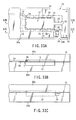
- FIG. 1A to FIG. 1E are figures which show the small antenna according to the first embodiment of the present invention.
- the small antenna according to the first embodiment is an antenna of the surface mounting type in which the planar antenna element 12 is embedded in the resin molded body 14.
- Thickness t1 of the resin molded body 14a (called as a, "lower part” for convenience' sake) on the circuit board side of the antenna element 12 (lower side of the antenna element 12 of FIG. 1B) is set in the necessary thickness so that the antenna element 12 is apart from the circuit board not to occur the influence of the characteristic lowering.
- Thickness t2 of the resin molded body 14b (called as an, "upper part” for convenience' sake) on the other side of the circuit board of the antenna element 12 (upper side of the antenna element 12 of FIG. 1B) is set in as thin as possible than the thickness t1.
- Thickness t2 is the minimum thickness necessary to protect the antenna element 12, for example.
- the gate portion 28 of the resin molding is provided to the upper side portion 14b with thin thickness of the resin molded body 14 (t2 side) in the first embodiment.
- the mark in this gate portion is actually called the gate portion 28 in this specification though mark 28 of the gate portion is a mark where the gate portion is removed after the resin molding.
- the gate portion 28 is provided on both sides of the resin molded body 14.
- the gate portion 28 may be provided at one end or both ends of the resin molded body 14.
- the gate portion 28 is also provided on the upper part 14b in which the thickness of the resin molded body 14 is thinner one (t2 side) in this case.
- the antenna element 12 is a rectangle and a planar.
- the feeder terminal part 16 and the ground terminal part 18 extended outside of the resin molded body 14 are formed on another end of the antenna element 12.
- the fixed terminal part 20 extended outside of the resin molded body 14 is formed on another end of the antenna element 12.
- Each of terminal parts 16, 18, and 20 is formed by being bent, so that the surface mounted on circuit board is almost the same level as the bottom of the resin molded body 14.
- the fixed terminal part 20 is provided if necessary, and might be omitted.
- a plurality of salients 12a are formed in a suitable interval on the both side ends of the antenna element 12.
- the resin molded body 14 which covers both sides of the antenna element 12 is integrally formed to continue in a part where there is no salient 12a. It is preferable that the resin molded body 14 which covers both sides of the antenna element 12 is continuously formed in the part without each terminal part 16, 18, and 20 on the both ends of the antenna element 12 as shown in the figure. However, these parts may be discontinuous.
- the small antenna of the surface mounting type as shown in FIG. 1A to FIG. 1E is manufactured as follows.
- the conductor pattern 10 as shown in FIG. 2 is formed by piercing processing or etching processing etc. of a metallic thin plate, first.
- the conductor pattern 10 has the frame 24 which surrounds the antenna element 12 and the circumference thereof.
- the antenna element 12 is a rectangle and a planar which consists of a metallic plate of about 0.1 mm in thickness, for example.
- the antenna element 12 and the frame 24 are connected by a plurality of the support parts 26, the feeder terminal part 16, the ground terminal part 18, and the fixed terminal part 20.
- a plurality of the support parts 26 are formed on the both side ends of the antenna element 12 in a suitable interval.
- the opening 50 is formed by the piercing processing etc. (The positioning hole for the piercing processing is omitted in the figure).
- the conductor pattern 10 is set in the molds 30a and 30b as shown in FIG. 3A and FIG. 3B. That is, the frame 24, the outside end side of each the support parts 26 and the outside end sides of each of terminal parts 16, 18 and 20 are placed in the parting faces of the upper mold 30a and the lower mold 30b.
- the conductor pattern 10 is set so that the entire antenna element 12, a part of end side in each the support part 26 and a part of end side in each terminal part 16 and 18 and 20 are positioned in the cavity of the upper and lower molds 30a and 30b.
- the depth of the cavity (Correspond to the thickness of the resin molded body) is shallowly formed with the lower mold 30b to mold the resin under the antenna element 12 (circuit board side).
- the resin flows easily into deeper side of the cavity usually when the depth of the cavity is different because of both sides of the antenna element 12 like this. Therefore, the resin pressure becomes unbalanced on both sides of the antenna element 12, and the deformation is occurred easily in the antenna element 12.
- the first embodiment solves this respect by providing the spool 33, the runner 34, and the gate 28 for the resin injection to the upper mold 30a side.
- the gate 28 is provided to be located to the opening 50 between the support parts 26 of the conductor pattern 10.
- FIG. 5A and FIG. 5B are figures which show the second embodiment of the present invention.
- the point where the second embodiment is different from the first embodiment is to form the part 14c whose thickness is thin at a part of the lower part 14a of the resin molded body.
- the part 14c whose thickness is thin is formed with the trench having the semicircle section formed over total length of the width direction of the antenna. Thickness t3 of the thinnest part of the part 14c whose thickness is thin is set to almost the same thickness as the thickness of the upper part 14b of the resin molded body.
- the part 14c whose thickness is thin is formed in the part of the lower part 14a of the resin molded body. Therefore, the resin flowing to the lower part 14a of the resin molded body can be limited more by the part 14c. As a result, the pressure balance when the lower part 14a and the upper part 14b of the resin molded body are molded becomes more excellent. Therefore, the antenna element 12 can be prevented from being deformed.
- the mark (gate portion) after the gate is cut may be in the same surface as the side surface of the resin molded body 14, may be projected or may be recessed as shown in FIG. 1A to FIG. 1E.
- FIG. 6 is a figure which shows the third embodiment of the manufacturing method of the small antenna according to the present invention.
- an interval d of a plurality of the support parts 26 which connect the antenna element 12 located in the cavity of the mold and the frame 24 which is held and fixed by the mold at the circumference thereof is wider at the position of the gate (position of gate part 28) and becomes narrow while being apart from the gate.
- the same marks are fixed to the same parts of FIG. 4, and a detailed explanation will be omitted since it is the same as the manufacturing method explained in the first embodiment.
- the resin filling pressure which is applied in the vicinity of the gate is easily spread to the lower mold 30b (FIG. 3A and FIG.
- FIG. 7 is a figure which shows the fourth embodiment of the manufacturing method of the small antenna according to the present invention.
- the gate (corresponding to the gate portion 28) is provided (In a word, only one gate is provided) only to the one side of the cavity in the fourth embodiment.
- the resin molded body 14 is formed by filling the resin from one gate. Besides, it is the same as the third embodiment. The opportunity that the flow of the resin injected thus at the injection molding intersects decreases. Therefore, the generation of the weld is suppressed, and the strength of the resin molded body can be improved.
- the gate may be provided at the lower mold 30b if necessary.
- the thickness of the resin molded body is thinned on the side of the other side (the upper part 14b) than on one side of the antenna element (the lower part 14a).
- the gate portion of the resin molding is provided to another side of the antenna element, that is, to thinner side of the resin molded body.
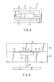
- FIG. 8 is a plan view which shows an example of the antenna element set in the mold.
- the same marks are fixed to the same parts as the first embodiment, and a detailed explanation will be omitted.
- the thickness of the resin molded body is thinner in another side of the antenna element than in one side thereof in the fifth embodiment as well as the first to fourth embodiments.
- the antenna element 12 is set in the molds 30a and 30b for injection molding as shown in FIG. 9 first as well as the first embodiment.
- the cavity 32b of the lower mold 30b is deeply formed with the cavity 32a of the upper mold 30a.
- the projection pin 36 to take out the resin molded body is provided to the lower mold 30b.
- the injection molding is performed by injecting the dielectric material in the cavity 32 in the state of FIG. 9.
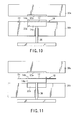
- the molds 30a and 30b are opened as shown in FIG. 10.
- the ejector pin 36 is projected as shown in FIG. 11, and the resin molded body 14 is taken out from the lower mold 30b.
- the ejector pin 36 pierces thicker side of the resin molded body 14 (with large strength, that is, lower part 14a). Therefore, even if the ejection speed of the ejector pin 36 is made fast, fear that the crack is generated in the resin molded body 14 and the deformation is occurred in the antenna element is a little.
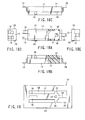
- each of terminal parts 16, 18, and 20 is cut off from the frame 24 and is bent.
- the small antenna shown in FIG. 12A and FIG. 12B is finally obtained.
- the small antenna manufactured like this has the incrustation of the projection pin under the resin molded body 14.
- the upper middle part of the resin molded body 14 sucked by the mounter becomes a smooth surface to which the mold surface is transferred. Therefore, there is no fear of the air leakage at picking-up, and the pickup mistake can be reduced.
- the projection pin is struck and ejected at lower surface (the lower part 14a) of the resin molded body when the resin molded body is taken out from the mold.
- the projection pin may be struck to the position where an upper position of arrow P, that is, the position avoiding the middle part as shown in FIG. 13 to prevent the pickup miss and the resin molded body may be ejected, when the projection pin is struck to the resin molded body and the resin molded body is taken out.
- the thicknesses of the resin molded body on both sides of the antenna element are deferent as well as the first embodiment, and the ejector pin is struck to the surface of the lower part 14a of the resin molded body and the resin molded body is ejected according to the fifth embodiment. Therefore, the strength of the resin molded body on the side where the ejector pin is struck increases. As a result, since it becomes possible to endure more high-speed projection operation, the production efficiency can be improved.
- the ejector pin is struck to the position where an upper middle part of the resin molded body is avoided and the resin molded body is ejected according to the fifth embodiment. Therefore, the position sucked by the mounter becomes a flat surface without the incrustation of the ejector pin in the small antenna manufactured from the manufacturing method according to the fifth embodiment. As a result, there is no fear of the air leakage when picking-up, and the pickup mistake can be reduced.
- FIG. 14A to FIG. 14E is a figure which shows the sixth embodiment of the present invention.
- the same marks are fixed to the same parts as the first embodiment, and a detailed explanation will be omitted.
- the gate part 28 is provided near the end portion inclined to (in other rectangular example of shown in the figure of inclined to it of the end portion of the antenna of element 10 on terminal 16 and 18 sides).
- the hole 22 is provided to the vicinity of the end portion (end portion on a fixed terminal 18 side in the example shown in the figure) far from the gate portion 28 of the resin molded body 14 of the antenna element 12.
- the resin on both sides of the antenna element 12 is continuous (integrated) in the hole 22.
- the deformation in the vicinity of the end portion far from the gate portion 28 of the antenna element 12 can be controlled with such a structure (details are described later).
- the hole 22 is formed at the middle of the width direction of the antenna element 12.
- a small antenna as shown in FIG. 14A to FIG. 14E is manufactured as follows.
- the conductor pattern 10 shown in FIG. 15 is formed by piercing processing or etching processing of a metallic thin plate.
- the conductor pattern 10 has a rectangular planar antenna element 12 and a frame 24 which surrounds the circumference thereof.
- the antenna element 12 and the frame 24 are connected by the feeder terminal part 16 and the ground terminal part 18 formed on one end of the antenna element 12, and the fixed terminal part 20 formed on another end of the antenna element 12.
- the hole 22 is formed in the vicinity of the end portion of the antenna element 12 at the fixed terminal part 20 sides.
- the opening 50 is formed by the piercing processing etc. (the positioning hole for piercing processing is omitted in the figure).
- the conductor pattern 10 is set in the molds 30a and 30b for injection molding as shown in FIG. 16A and FIG. 16B, etc. as well as the first embodiment.
- the gate is provided to an upper side of the antenna element 12 in this embodiment.
- the resin which entered in the cavity 32 from the gate 28 is rapidly filled in the cavity 32, and flows on an upper side and a lower side of the antenna element 12. And, the flow of the resin changes greatly at the place where the front of the flow of the resin strikes the wall of the cavity 32 far from the gate 28.
- the depths of the cavity 32 thickness of the resin
- the injection pressure and flow velocity of the resin at the upper and the lower sides of the antenna element 12 are different. Therefore, the reach time of the resin to the cavity end portion far from the gate 28 is also different.
- the change of the flow of the resin is enlarged at the cavity end portion far from the gate 28.
- the hole 22 is formed to the antenna element 12 as described above, the resin can pass through the hole 22. Therefore, the unbalance of the resin pressure is reduced on both sides of the antenna element 12. Therefore, it can be controlled to occur the deformation of the antenna element 12 in the vicinity of the end portion far from the gate 28.
- the small antenna of FIG. 14A to FIG. 14E is formed so that the thickness of the resin molded body 14 is thick on the lower part 14a of the antenna element 12 (circuit board side) and is thin on the upper part 14b thereof as well as the first embodiment. But, the thickness of the resin molded body 14 needs not differ in the lower part 14a and the upper part 14b. When the thickness of the resin molded body 14 is different on both sides of the antenna element 12 as in the sixth embodiment, it is preferable to provide the gate portion 28 to thinner side to reduce the deformation of the antenna element 12 further.
- the resin molded body 14 may be projected or recessed and may be in the same plane as the side surface of the resin molded body 14 as shown in FIG. 14A to FIG. 14E.
- the gate 28 is provided to both sides of the resin molded body 14 in the sixth embodiment, the gate 28 may be provided on one side of the resin molded body 14.
- FIG. 18A to FIG. 18E are figures which show the seventh embodiment of the present invention.
- the same marks are fixed to the same parts as FIG. 14A to FIG. 14E.
- the point where the small antenna according to the seventh embodiment is different from a small antenna of the sixth embodiment is that the projection 40 is provided on the both side ends of the part to which the hole 22 of the antenna element 12 is provided. The strength lowering of the antenna element 12 by providing the hole 22 is supplemented by the projection 40, and the deformation of the antenna element 12 near the hole 22 is decreased more.
- the small antenna of FIG. 18A to FIG. 18E can be manufactured as follows. First, the conductor pattern 10 as shown in FIG. 19 is formed. In the conductor pattern 10, both side ends of the part to which the hole 22 of the antenna element 12 is provided and the frame 24 are connected by the bridge part 26 (support part). Besides, it is the same as the conductor pattern 10 of FIG. 15.
- the conductor pattern 10 is set in the molds 30a and 30b as shown in FIG. 20.
- the molds 30a and 30b in FIG. 20 are the same as the molds 30a and 30b in FIG. 16A and FIG. 16B.
- the method of setting the conductor pattern 10 to the molds 30a and 30b is also the same as FIG. 16A and FIG. 16B.
- the resin molding by injecting the resin in the state of FIG. 20. Fear that the antenna element 12 is deformed near the hole 22 when the resin molding is a little in a case of FIG. 20, since the bridge part 26 is placed between the molds 30a and 30b and pressed thereby.
- the small antenna as shown in FIG. 18A to FIG. 18E can be obtained by performing a similar cutting processing and bending processing to the sixth embodiment after the resin molding.
- the projection 40 in FIG. 18A to FIG. 18E is a part in which the bridge part 26 is cut and is left in the resin molded body 14.
- the hole is provided to the antenna element in a small antenna in which a planar antenna element is embedded in the resin molded body according to the sixth embodiment and the seventh embodiment.
- FIG. 21A to FIG. 21D are figures which show the eighth embodiment of the present invention.
- the planar antenna element 12 is embedded in the resin molded body 14 as well as the first embodiment in the small antenna according to the eighth embodiment.
- the feeder terminal part 16 and the ground terminal part 18 extended from one end of the antenna element 12 are bent and are molded at the outside of the resin molded body 14 which is dielectric.
- the small antenna according to the eighth embodiment has the feature in the point that the narrowed portion 42 with narrow width of the conductor is provided to the bent part at the end surface of the resin molded body 14 of the feeder terminal part 16 and the ground terminal part 18.
- the feeder terminal part 16 and the ground terminal part 18 are bent in the end surface of the resin molded body 14, it is possible to bend them by the small power, when the narrowed portion 42 is provided on the base portion. In addition, the strength of the resin molded body therearound improves, too. Therefore, the crack of the resin molded body can be controlled.
- the configuration of the eighth embodiment is especially preferable, when the antenna element is formed by performing the copper plating to the board material of high strength which comprises the phosphorus bronze, and the iron, etc. used also for the spring material.
- FIG. 22A to FIG. 22D are figures which show the ninth embodiment of the present invention.
- the small antenna according to the ninth embodiment also comprises a configuration in which the planar antenna element 12 is embedded in the resin molded body 14 the feeder terminal part 16 and the ground terminal part 18 are extended from the antenna element 12 as well as the first embodiment.
- the base portion side of the feeder terminal part 16 and the ground terminal part 18 are integrated.
- the narrowed portion 42 whose conductor width is narrow is provided on the integrated part 44, and the narrowed portion 42 is bent at the end of the resin molded body.
- the previous state to which each of terminal parts 16, 18, and 20 are bent is FIG. 23A and FIG. 23B.
- the ninth embodiment has the advantage of generating the crack of the resin molded body 14 hardly than the case of the eighth embodiment.
- FIG. 24A and FIG. 24B are figures which show the tenth embodiment of the present invention.
- the point where the small antenna according to the tenth embodiment is different from the small antenna according to the eighth embodiment is that the antenna elements 12 are accumulated on the surface of the resin molded body (dielectric material) 14. Even in the small antenna having such a configuration, the same effect as the small antenna of the eighth embodiment can be achieved.
- the narrowed portion 42 is provided to the bent part of the terminal drawn out from the dielectric material at the end surface of the dielectric material.
- the power applied to dielectric material when the terminal part is bent can be reduced.
- the strength of dielectric material therearound can be improved. Therefore, the crack of dielectric material can be controlled. Therefore, the product yield can be improved, and the manufacturing cost can be reduced.
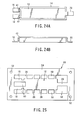
- FIG. 25 is a figure which shows the eleventh embodiment of the present invention.
- the conductor pattern 10 as shown in FIG. 25 is formed by performing the piercing processing or the etching processing of the metallic thin plate to the small antenna according to the eleventh embodiment, first, as well as the first embodiment.
- the conductor pattern 10 has the antenna element 12 and a frame 24 which surrounds the circumference thereof.
- the antenna element 12 and the frame 24 are connected by a plurality of the support parts 26 formed on the both side ends of the antenna element 12 in a suitable interval, the feeder terminal part 16 and the ground terminal part 18 formed on one end of the antenna element 12, and the fixed terminal part 20 formed on another end of the antenna element 12.
- the opening 50 and the positioning hole 52 formed by the piercing processing etc. are shown in FIG. 25.
- FIG. 25 it is also possible to omit the frame 24. However, it is preferable to restrict the limit of begin the expansion in the part molded by handle of the conductor pattern 10 an easy, as for there is the frame 24 extra resin as described later.
- the fixed terminal part 20 is provided if necessary, and can also be omitted.
- the ground terminal part 18 may be omitted according to the kind of the antenna element (for example, it is unnecessary when the antenna element is the meander antenna element, etc.).
- the conductor pattern 10 is set in the molds 30a and 30b based on the positioning pin 56 of the lower mold 30b as shown in FIG. 26 to FIG. 28. That is, the frame 24, the outside end side of the support parts 26 and the outside end sides of each terminal part 16, 18 and 20 are placed between the parting faces of the upper mold 30a and the lower mold 30b. And, the antenna element, a part of the end side of each support part 26, and a part of the end side of each terminal part 16, 18 and 20 are set to be located partly in the cavity 32 of the molds 30a and 30b. In the eleventh embodiment, the parting faces at the circumference of the cavity 32 of the molds 30a and 30b are flattened.
- the space S which is led to the cavity 32 is appeared by placing the conductor pattern 10 between the molds 30a and 30b in the part (part where the frame 24, the support part 26, the terminal parts 16, 18, and 20 are not placed) which corresponds to the opening 50 of the conductor pattern 10 between in the parting faces of the molds 30a and 30b.
- the resin molded body integrated with the conductor pattern 10 taken out by opening the molds 30a and 30b after molding is shown in FIG. 29.
- the antenna element 12 is embedded in the resin molded body 14 according to FIG. 29.
- the part 54 (hereinafter, called as a "fin") molded in the opening 50 of the circumference of the resin molded body 14 by an extra resin of the same thickness as the conductor pattern 10 is formed.
- the conductor pattern 10 has the frame 24 in circumference thereof. Therefore, the fin 54 is extended only to the inner end of the frame 24 even if it is the maximum. In a word, the frame 24 restricts the limit of begin the extension of the fin 54, and has the function to prevent the resin from being leaked to outside of the molds 30a and 30b at the resin molding.
- the fin 54 is essentially unnecessary, but has a secondary effect which can be judged whether the molding condition is proper as a result of the fin 54.
- the support parts 26 and the fin 54 are cut along both sides of the resin molded body 14.
- the outside ends of each of terminal parts 16, 18, and 20 are cut off from the frame 24 and are bent.
- a small antenna as shown in FIG. 30A to FIG. 30D can be obtained.
- the antenna element 12 is embedded in the resin molded body 14.
- the feeder terminal part 16 and the ground terminal part 18 are extended from one end surface of the resin molded body 14.
- the fixed terminal part 20 is extended from another end surface of the resin molded body 14.
- the lower part 14a of the resin molded body 14 is thicker than that of the upper part 14b.
- FIG. 31 is a figure which shows the twelfth embodiment of the present invention.
- the point where the twelfth embodiment is different from the eleventh embodiment is that the antenna element 12 and the frame 24 are connected only by the terminal parts 16, 18, and 20, and the conductor pattern 10 to which the support parts 26 is not provided is used.
- the end of in the fixed terminal part 20 side of the antenna element 12, the feeder terminal part 16, and the ground terminal part 18 are placed between the parting faces of the upper and lower molds 30a and 30b.
- the space is formed in the part where the antenna element, etc. are not placed between the parting faces of the upper and lower molds 30a and 30b.
- the resin is injected, the point that an extra resin flows into the space is the same as the eleventh embodiment. Therefore, the same effect as the eleventh embodiment can be achieved by the twelfth embodiment.
- FIG. 32 is a figure which shows the thirteenth embodiment of the present invention.
- FIG. 32 is a state when the molding step ends.
- the point where the thirteenth embodiment is different from the eleventh embodiment is to use the conductor pattern 10 in which each of terminal parts 16, 18, and 20 are not connected with the frame 24.
- the mold 30, which forms the salient engaged with the opening 50 of the circumference of each of terminal parts 16, 18, and 20, is used for the parting face of the lower mold 30b.
- the resin is prevented from flowing into the opening 50 of the circumference of each of terminal parts 16, 18, and 20 by the salient formed to the lower mold 30b. Therefore, the fin 54 is not formed to the opening 50.
- the resin can be prevented from adhering to the terminal parts 16, 18, and 20. Therefore, the plating processing to the terminal part performed by the post-processing and the bend processing of the terminal part, etc. become easy. Since the terminal parts 16, 18, and 20 are separated from the frame 24 beforehand, the plating processing to the entire surface the circumference surface (cutting surface) of the terminal part becomes easy, too.
- FIG. 33A to FIG. 33C are figures which show the fourteenth embodiment of the present invention.
- the resin receiver 38 which is led to the cavity 32 is formed at the side of the cavity 32 of the lower mold 30b.
- the resin receiver 38 is led to the cavity by the narrow opening part 38a.
- An entrance of the opening part 38a is little deeper than the interval of the space S and becomes wider from the entrance toward the interior.
- the wide space 38b is formed to the depth part.
- the resin receiver 38 is provided to a position different from the support part 26.
- the entrance of the resin receiver 38 is formed to 1 mm in width and 0.5 mm in depth.
- the thickness of the conductor pattern 10 is 0.127 mm.
- the size of the entire antenna is 2 mm in width, 15 mm in length, and 2.8 mm in thickness, or 4 mm in width, 8 mm in length, and 2.8 mm in thickness. Besides, the same marks are fixed to the same parts since it is similar to the eleventh embodiment.
- the support parts 26 and the resin receiver 38 are adjusted to different positions not to overlap the different materials in the fourteenth embodiment. Therefore, the removal work of the support parts 26 and the resin receiver 38 is easy.
- the thickness of the conductor pattern 10 is adjusted to 0.13 mm or less, when the resin with bad liquidity in which a ceramic powder is mixed, for example, is injection-molded to improve the permittivity, the generation of fin can be suppressed.
- the resin receiver 38 is folded later and is removed. As mentioned above, since opening part 38a of the resin receiver 38 has a taper-shape, this removal work is easy.
- FIG. 35A to FIG. 35C are figures which show the fifteenth embodiment of the present invention.
- the parting face of the upper mold is flat as well as FIG. 33A to FIG. 33C, though only the lower mold 30b is shown in FIG. 35A to FIG. 35C.
- the point where the fifteenth embodiment is different from the fourteenth embodiment is to use the mold which forms the salient 58 engaged with the opening 50 in both vicinity of each of terminal parts 16, 18, and 20 (see FIG. 36) for the parting faces of the lower mold 30b.
- the thickness of salient 58 is set to the same thickness as the conductor pattern 10 or some thinner than it.
- FIG. 36 shows the state that the resin molded body 14 which is molded by the above-mentioned molding and is integrated with the conductor pattern 10 is taken out from the mold.
- the part 38' molded by the resin receiver 38 of the resin molded body 14 is cut off later together with the support parts 26 etc.
- the insert molding of the antenna element is performed in the state of providing the space to which the resin can flow between in the parting faces of the mold and the resin receiver. Therefore, the resin pressure in the mold is not raised too much and the residual stress of the resin molded body becomes small, too. Therefore, the deformation of the antenna element caused by the resin pressure in the mold and the residual stress of the resin molded body can be controlled. Therefore, the small antenna with stable characteristic can be efficiently manufactured. Since the product yield improves, the manufacturing cost can be reduced.
- FIG. 37 is an upper view of the small antenna according to the sixteenth embodiment of the present invention immediately after the molding
- FIG. 38 is a side view of the small antenna according to the sixteenth embodiment of the present invention
- FIG. 39 is a method of taking out a small antenna of FIG. 37 from the mold.
- the same marks are fixed to the same parts as each above-mentioned embodiment.
- the small antenna according to the sixteenth embodiment is an antenna of the surface mounting type which shows the planar antenna element 12 is embedded in the resin molded body 14.
- the thickness of the lower part 14a of the resin molded body 14 of the antenna element 12 is set in the thickness necessary so that the circuit board is separated from the antenna element 12 not to generate the influence of the characteristic lowering of the antenna element 12.
- the thickness of the upper part 14b of the resin molded body 14 of the antenna element 12 is set to a thickness as thin as possible than the lower part 14a.
- the thickness of the upper part 14b is, for example, the lowest thickness necessary to protect the antenna element 12. As a result, it is possible to miniaturize the small antenna by thinning the resin molded body.
- the gate portion 28 is provided to the upper part 14b of the resin molded body 14 at the resin molding in the sixteenth embodiment.
- the small antenna with little deformation of the antenna element and stable characteristic can be obtained by such a configuration. It is preferable that an interval d of plurality of the support part 26 which connects the antenna element 12 located in the cavity of the mold and the frame 24 to the mold by the circumference is wider at the position of the gate (position of gate part 28) and becomes narrow while being apart from the gate. As a result, the unbalance of the resin pressure which is applied upper and lower surfaces of the antenna element 12 from the filling final step to the pressure-maintaining step is relaxed. Therefore, the antenna element 12 can be prevented from being deformed by the resin pressure to the antenna element 12.
- the hole 22 is provided in the vicinity of the end portion (it is a end portion on a fixed terminal 18 side in the example of shown in the figure) far from the gate portion 28 of the resin molded body 14 of the antenna element 12 in the small antenna according to the sixteenth embodiment.
- the hole 22 is formed at the middle of the width direction of the antenna element 12.
- the resin on both sides of the antenna element 12 is continuous (integrated) in the hole 22.
- the deformation in the vicinity of the end portion far from the gate portion 28 of the antenna element 12 can be controlled by such a structure. Therefore, the small antenna with little difference in characteristic can be provided.
- the resin molded body might be cracked in this case.
- the power applied to dielectric material when the terminal part is bent can be reduced.
- the strength of the dielectric material in the vicinity thereof can be improved. Therefore, the crack of dielectric material can be controlled. Therefore, the product yield can be improved, and the manufacturing cost can be reduced.
- planar antenna element is shown as the antenna element 12 in each above-mentioned embodiment.
- the compound material which enables the injection molding by mixing the resin and ceramics, though the dielectric material is not especially limited.
- the small antenna according to the first aspect is characterized by comprising: a planar antenna element; and a resin molded body integrally molded with the antenna element, in which the resin molded body has a thin part and a thick part on both sides of the antenna element, and a gate portion at a resin molding is provided to the thin part.
- the necessary thickness of the resin molded body is secured at one surface side of the antenna element and the thickness of another side of the antenna element of the resin molded body is thinner than that of one surface side.
- the thickness of the resin molded body can be thinned as a whole.
- the deformation of the antenna element can be controlled by providing the gate portion of the resin molding to the thinner side of the resin molded body. It is thought that the resin comes to be supplied enough to thinner side when the resin molded body is molded, and the resin pressure on both sides of the antenna element is more balanced, though this reason is not clear.
- the thin part is provided on a part of the thick part of the antenna element in the first aspect.
- the resin flowing to one surface side can be limited further by partially providing the thin part to one surface side of the antenna element, that is, the side where the thick resin molded body is formed. Therefore, the deformation of the antenna element can be more reduced.
- the small antenna according to the second aspect is characterized by comprising: a planar antenna element; a resin molded body integrally molded with the antenna element; and a hole formed to the antenna element.
- the balance of the resin pressure is not kept off greatly on both sides of the antenna element 12 by providing the hole. Therefore, the small antenna with little deformation of the antenna element can be obtained.
- a projection formed on both side ends of a part where the hole of the antenna element is provided is further comprised. It is preferable to provide the "hole” in the vicinity of both ends, when the gate portion is in the vicinity of a middle part of the antenna element. However, even if the "hole” is provided in the vicinity of either end portion a good result is obtained than the case that the "hole” is not provided,.
- the hole of the antenna element is provided to an end portion side far from the gate portion of the resin molded body.
- the strength in the corresponding part lowers and the deformation might be occurred. Therefore, the projection as mentioned above is formed, and the projection is placed between the molds. As a result, the antenna element can be prevented from being deformed by forming the hole.
- the small antenna according to the third aspect is characterized by comprising: an antenna element; and a resin molded body in which the antenna element is embedded or which is accumulated, the antenna element having a terminal extended to an outside of the resin molded body, in which the terminal comprises a narrowed portion with narrow width of a conductor at a base thereof, and the narrowed portion is bent at an outside of the resin molded body.
- the part drawn out from the dielectric material is bent in the end surface of dielectric material, it is possible to bend by the smaller power by providing the narrowed portion.
- the strength in the vicinity of the dielectric material can be improved. Therefore, the crack of the dielectric material is not generated easily.
- the crack is generated easily in the part of the dielectric material located between the feeder terminal and the ground terminal especially, in the antenna having the configuration in which the feeder terminal and the ground terminal are extended from the side of the antenna element. It is preferable that a base side of a feeder terminal and a ground terminal extended from the antenna element are integrated, and the narrowed portion with the narrow width of the conductor is provided to the integration part for the above-mentioned antenna. With this configuration, it becomes the same state as performing the bend processing of one terminal, since there is no the part of the dielectric material placed between two terminals. Therefore, the crack of the dielectric material is generated more hardly.
- the manufacturing method of the small antenna according to the fourth aspect is characterized by comprising: setting an antenna element to place the antenna element between a first mold and a second mold of the mold; and integrally molding a resin molded body to embed the antenna element by injecting the resin to the mold, in which a depth of a cavity of the first mold is shallower than a depth of a cavity of the second the mold, and a gate portion is provided to the first mold.
- a depth of a cavity of the first mold is shallower than a depth of a cavity of the second the mold, and a gate portion is provided to the first mold.
- an interval of support parts which connects the antenna element set in the cavity of the mold and a frame placed between the mold at a circumference thereof is wide at a position of the gate portion and becomes narrow apart from the gate portion in the fourth aspect.
- the manufacturing method of the small antenna according to the fifth aspect is characterized by comprising: setting an antenna element in a mold; performing injection molding by injecting a resin which is a dielectric material in the mold; and ejecting a resin molded body by striking an ejector pin to the resin molded body, when the mold is opened and the resin molded body after the injection molding is taken out, in which the resin molded body has the surfaces whose thickness are different at both sides of the antenna element, and ejecting including striking the ejector pin to a thicker surface of the resin molded body and ejecting the resin molded body.
- the manufacturing method of the small antenna according to the sixth aspect is characterized by comprising: setting an antenna element in a mold; performing injection molding by injecting a resin which is dielectric material in the mold; and ejecting a resin molded body by striking an ejector pin to the resin molded body, when the mold is opened and the resin molded body after the injection molding is taken out, in which ejecting includes striking the ejector pin to a position where a part to which the resin molded body is picked up is avoided and ejecting the resin molded body. Since the position sucked by the mounter becomes a flat surface without the incrustation of the ejector pin in the small antenna manufactured as mentioned above, there is no fear of the air leakage at picking-up, and the pickup mistake can be reduced.
- a compound material of a resin and a ceramics is used as the dielectric material in the fifth aspect and the sixth aspects.
- a practicable small antenna can be efficiently manufactured by the injection molding method, since such a compound material has the high permittivity, in addition, excellent stability in the temperature and the humidity, and the injection molding is possible.
- the manufacturing method of the small antenna according to the seventh aspect is characterized by comprising: setting an antenna element by placing at least a part between parting faces of a mold; and injecting a resin in the mold, in which setting includes setting the antenna element to form a space in a part where the antenna element is not placed in the parting faces.
- the manufacturing method of the small antenna according to the eighth aspect is characterized by comprising: setting an antenna element by placing at least a part between parting faces of the mold; and injecting a resin in the mold and performing a molding, in which a plurality of support parts extended to an outside to at least two opposite sides in the antenna element are integrally formed, and setting includes setting the antenna element to place the support parts between the parting faces of the mold in the parting faces, and form a space in a part where the support parts between the parting faces of the mold is not placed.
- the support parts are formed to connect between the antenna element and a frame which surrounds a circumference thereof, and the resin molding is performed in a state that the support parts and the frame placed between the parting faces of the mold in the seventh aspect and the eighth aspect.
- the mold has a flat parting faces to decrease the mold cost as the mold in each above-mentioned aspect.
- the part molded by the extra resin is generated to the space at the resin molding in each above-mentioned aspect. It is preferable to take out the resin molded body from the mold after molding; and cut off and remove a part which is molded by the space with the support part and is projected to an outside of the resin molded body. This part can be easily removed by cutting it at the same time when the support parts projected to the outside of the resin molded body is cut, after the resin molded body is taken out from the mold.
- the mold has a resin receiver which is led to the cavity at a side of the cavity of the mold in each above-mentioned aspect.
- the same effect as the fin can be achieved by providing such a resin receiver and flowing the extra resin thereto.
- the effect same as the fin can be achieved.
Abstract
Description
- The present invention relates to a small antenna and a manufacturing method thereof used for small telecommunication equipment such as cellular phones.
- In a small antenna, the miniaturization is requested as much as possible to reduce the mounting area to a circuit board, etc. A small antenna is mounted in small telecommunication equipments such as cellular phones. Therefore, it is requested to a small antenna that thickness thereof is as thin as possible in addition to the miniaturization.
- It is considered that the following molding methods, so-called the insert molding method is employed to this kind of the small antenna. That is, the antenna element is integrated with the resin molded body by setting the antenna element formed to the necessary shape in the mold and injecting the resin.
- In a small antenna as mentioned above, the strength of the small antenna lowers, when the area of the antenna element is reduced as much as possible or the thickness of the resin molded body is thinned as much as possible to miniaturize the antenna. Therefore, the antenna becomes easily deformed when producing. The deformation of the antenna influences the impedance characteristic of the antenna. Therefore, it is important to prevent the deformation when the antenna is produced.
- An object of the present invention is to provide a small antenna and a manufacturing method thereof, in which the crack of the resin molded body and the deformation of the antenna element are hardly generated.
- The small antenna according to the first aspect of the present invention is characterized by comprising: a planar antenna element; and a resin molded body integrally molded with the antenna element, in which the resin molded body has a thin part and a thick part on both sides of the antenna element, and a gate portion at a resin molding is provided to the thin part.
- The small antenna according to the second aspect of the present invention is characterized by comprising: a planar antenna element; a resin molded body integrally molded with the antenna element; and a hole formed to the antenna element.
- The small antenna according to the third aspect of the present invention is characterized by comprising: an antenna element; and a resin molded body in which the antenna element is embedded or which is accumulated, the antenna element having a terminal extended to an outside of the resin molded body, in which the terminal comprises a narrowed portion with narrow width of a conductor at a base thereof, and the narrowed portion is bent at an outside of the resin molded body.
- The manufacturing method of the small antenna according to the fourth aspect of the present invention is characterized by comprising: setting an antenna element to place the antenna element between a first mold and a second mold of the mold; and integrally molding a resin molded body to embed the antenna element by injecting the resin to the mold, in which a depth of a cavity of the first mold is shallower than a depth of a cavity of the second the mold, and a gate portion is provided to the first mold.
- The manufacturing method of the small antenna according to the fifth aspect of the present invention is characterized by comprising: setting an antenna element in a mold; performing injection molding by injecting a resin which is a dielectric material in the mold; and ejecting a resin molded body by striking an ejector pin to the resin molded body, when the mold is opened and the resin molded body after the injection molding is taken out, in which the resin molded body has the surfaces whose thickness are different at both sides of the antenna element, and ejecting including striking the ejector pin to a thicker surface of the resin molded body and ejecting the resin molded body.
- The manufacturing method of the small antenna according to the sixth aspect of the present invention is characterized by comprising: setting an antenna element in a mold; performing injection molding by injecting a resin which is dielectric material in the mold; and ejecting a resin molded body by striking an ejector pin to the resin molded body, when the mold is opened and the resin molded body after the injection molding is taken out, in which ejecting includes striking the ejector pin to a position where a part to which the resin molded body is picked up is avoided and ejecting the resin molded body.
- The manufacturing method of the small antenna according to the seventh aspect of the present invention is characterized by comprising: setting an antenna element by placing at least a part between parting faces of a mold; and injecting a resin in the mold, in which setting includes setting the antenna element to form a space in a part where the antenna element is not placed in the parting faces.
- The manufacturing method of the small antenna according to the eighth aspect of the present invention is characterized by comprising: setting an antenna element by placing at least a part between parting faces of the mold; and injecting a resin in the mold and performing a molding, in which a plurality of support parts extended to an outside to at least two opposite sides in the antenna element are integrally formed, and setting includes setting the antenna element to place the support parts between the parting faces of the mold in the parting faces, and form a space in a part where the support parts between the parting faces of the mold is not placed.
- This summary of the invention does not necessarily describe all necessary features so that the invention may also be a sub-combination of these described features.
- The invention can be more fully understood from the following detailed description when taken in conjunction with the accompanying drawings, in which:
- FIG. 1A to FIG. 1E are figures which show the small antenna according to the first embodiment of the present invention, and FIG. 1A to FIG. 1E are a plan view, a front view, a rear view, a left view, and a right view, respectively;
- FIG. 2 is a plan view of the conductor pattern used for the first embodiment of the manufacturing method according to the present invention;
- FIG. 3A and FIG. 3B are figures which show the states to set the conductor pattern of FIG. 2 in the mold, and FIG. 3A is a horizontal sectional view and FIG. 3B is a vertical sectional view;
- FIG. 4 is a plan view which shows a state to take out the resin molded body integrated with the conductor pattern of FIG. 2 from the mold;
- FIG. 5A and FIG. 5B are figures which show the second embodiment of the small antenna according to the present invention, FIG. 5A is a front view and FIG. 5B is a bottom view;
- FIG. 6 is a figure which shows the third embodiment of the manufacturing method of the small antenna according to the present invention;
- FIG. 7 is a figure which shows the fourth embodiment of the manufacturing method of the small antenna according to the present invention;
- FIG. 8 is a plan view which shows an example of the antenna element used for the fifth embodiment of the present invention;
- FIG. 9 is a sectional view which shows the state to set the antenna element in the mold in the fifth embodiment of the present invention;
- FIG. 10 is a sectional view which shows the state to open the mold after injection molding in the fifth embodiment of the present invention;
- FIG. 11 is a sectional view which shows the state to take out the resin molded body from the mold in the fifth embodiment of the present invention;
- FIG. 12A and FIG. 12B are figures which show the small antenna manufactured in the fifth embodiment of the present invention, FIG. 12A is a plan view, and FIG. 12B is a front view;
- FIG. 13 is a figure which shows the modification of the fifth embodiment of the present invention, and is an explanation figure which shows the projection position of the projection pin;
- FIG. 14A to FIG. 14E are figures which show the sixth embodiment of the small antenna according to the present invention, FIG. 14A is a plan view, FIG. 14B is a partly cutaway front view, FIG. 14 C is a rear view, FIG. 14D is a left side view, and FIG. 14E is a right side view;
- FIG. 15 is a plan view which shows the conductor pattern used to manufacture the small antenna of FIG. 14A to FIG. 14E;
- FIG. 16A and FIG. 16B are figures which show the state to set the conductor pattern of FIG. 15 in the mold, FIG. 16A is a horizontal sectional view, and FIG. 16B is a vertical sectional view;
- FIG. 17 is a plan view which shows the state to take out the molded body from the mold after the resin molding by the mold of FIG. 16A and FIG. 16B;
- FIG. 18A to FIG. 18E are figures which show the seventh embodiment of the small antenna according to the present invention, FIG. 18A is a partly cutaway plan view, FIG. 18B is a partly cutaway front view, FIG. 18C is a rear view, FIG. 18D is a left side view, and FIG. 18E is a right side view;
- FIG. 19 is a plan view which shows the conductor pattern used to manufacture the small antenna of FIG. 18A to FIG. 18E;
- FIG. 20 is a horizontal sectional view which shows the state to set the conductor pattern of FIG. 19 in the mold;
- FIG. 21A to FIG. 21D are figures which show the eighth embodiment of the small antenna according to the present invention, FIG. 21A is a partly cutaway plan view, FIG. 21B is a front view, FIG. 21C is a left side view, and FIG. 21D is a right side view;
- FIG. 22A to FIG. 22D are figures which show the ninth embodiment of the small antenna according to the present invention, FIG. 22A is a partly cutaway plan view, FIG. 22B is a front view, FIG. 22C is a left side view, and FIG. 22D is a right side view;
- FIG. 23A and FIG. 23B are figures which show a half-finished goods in a process of manufacturing the small antenna of FIG. 22A to FIG. 22D, FIG. 23A is a partly cutaway plan view, and FIG. 23B is a front view;
- FIG. 24A and FIG. 24B are figures which show the tenth embodiment of the small antenna according to the present invention, FIG. 24A is a plan view, and FIG. 24B is a front view;
- FIG. 25 is a plan view of the conductor pattern including the antenna element used for the eleventh embodiment of the present invention;
- FIG. 26 is a horizontal sectional view which shows the state to set the conductor pattern of FIG. 25 in the mold;
- FIG. 27A to FIG. 27C are sectional views which show a sectional view cut along 27A-27A line, a sectional view cut along 27B-27B line, and a sectional view cut along 27C-27C line in FIG. 26, respectively;
- FIG. 28 is a sectional view cut along 28-28 line in FIG. 27B;
- FIG. 29 is a plan view which shows the state to take out the resin molded body integrated with the conductor pattern of FIG. 25 from the mold;
- FIG. 30A to FIG. 30D are figures which show an example of the small antenna manufactured from the manufacturing method of the present invention, FIG. 30A is a plan view, FIG. 30B is a side view, FIG. 30C is a rear view, and FIG. 30D is a front view;
- FIG. 31 is a horizontal sectional view which shows the twelfth embodiment of the present invention in a state of setting the conductor pattern in the mold;
- FIG. 32 is a plan view which shows the thirteenth embodiment of the present invention in the state of taking out the resin molded body integrated with the conductor pattern from the mold;
- FIG. 33A to FIG. 33C are figures which show the conductor pattern set in the mold according to the fourteenth embodiment of the present invention, FIG. 33A is a subject cutaway plan view, and FIG. 33B is a sectional view cut along 33B-33B line in FIG. 33A and FIG. 33C is a sectional view cut along 33C-33C line in FIG. 33A;
- FIG. 34 shows the manufacturing method of FIG. 33A to FIG. 33C and are plan views which show the state to take out the resin molded body integrated with the conductor pattern from the mold;
- FIG. 35A to FIG. 35C are figures which show a lower mold used in the fifteenth embodiment of the present invention, FIG. 35A is a plan view FIG, and FIG. 35B is a sectional view cut along 35B-35B line in FIG. 35A and FIG. 35C is a sectional view cut along 35C-35C line in FIG. 35A;
- FIG. 36 is a plan view which shows the state to take out the resin molded body which is molded by the mold of FIG. 35A to FIG. 35C and integrated with the conductor pattern, from the mold;
- FIG. 37 is an upper view of the small antenna according to the sixteenth embodiment of the present invention immediately after the molding;
- FIG. 38 is a side view of the small antenna according to the sixteenth embodiment of the present invention; and
- FIG. 39 is a figure which shows the method of taking out the small antenna of FIG. 37 from the mold.
-
- Hereinafter, embodiments of the present invention will be explained in detail referring to the drawings.
- FIG. 1A to FIG. 1E are figures which show the small antenna according to the first embodiment of the present invention. The small antenna according to the first embodiment is an antenna of the surface mounting type in which the
planar antenna element 12 is embedded in the resin moldedbody 14. - Thickness t1 of the resin molded
body 14a (called as a, "lower part" for convenience' sake) on the circuit board side of the antenna element 12 (lower side of theantenna element 12 of FIG. 1B) is set in the necessary thickness so that theantenna element 12 is apart from the circuit board not to occur the influence of the characteristic lowering. Thickness t2 of the resin moldedbody 14b (called as an, "upper part" for convenience' sake) on the other side of the circuit board of the antenna element 12 (upper side of theantenna element 12 of FIG. 1B) is set in as thin as possible than the thickness t1. Thickness t2 is the minimum thickness necessary to protect theantenna element 12, for example. Thegate portion 28 of the resin molding is provided to theupper side portion 14b with thin thickness of the resin molded body 14 (t2 side) in the first embodiment. In FIG. 1A to FIG. 1E, there is a case that the mark in this gate portion is actually called thegate portion 28 in this specification thoughmark 28 of the gate portion is a mark where the gate portion is removed after the resin molding. In FIG. 1A to FIG. 1E, thegate portion 28 is provided on both sides of the resin moldedbody 14. Thegate portion 28 may be provided at one end or both ends of the resin moldedbody 14. Thegate portion 28 is also provided on theupper part 14b in which the thickness of the resin moldedbody 14 is thinner one (t2 side) in this case. - The
antenna element 12 is a rectangle and a planar. Thefeeder terminal part 16 and theground terminal part 18 extended outside of the resin moldedbody 14 are formed on another end of theantenna element 12. The fixedterminal part 20 extended outside of the resin moldedbody 14 is formed on another end of theantenna element 12. Each ofterminal parts body 14. The fixedterminal part 20 is provided if necessary, and might be omitted. A plurality ofsalients 12a are formed in a suitable interval on the both side ends of theantenna element 12. The resin moldedbody 14 which covers both sides of theantenna element 12 is integrally formed to continue in a part where there is no salient 12a. It is preferable that the resin moldedbody 14 which covers both sides of theantenna element 12 is continuously formed in the part without eachterminal part antenna element 12 as shown in the figure. However, these parts may be discontinuous. - The small antenna of the surface mounting type as shown in FIG. 1A to FIG. 1E is manufactured as follows. The
conductor pattern 10 as shown in FIG. 2 is formed by piercing processing or etching processing etc. of a metallic thin plate, first. Theconductor pattern 10 has theframe 24 which surrounds theantenna element 12 and the circumference thereof. Theantenna element 12 is a rectangle and a planar which consists of a metallic plate of about 0.1 mm in thickness, for example. Theantenna element 12 and theframe 24 are connected by a plurality of thesupport parts 26, thefeeder terminal part 16, theground terminal part 18, and the fixedterminal part 20. A plurality of thesupport parts 26 are formed on the both side ends of theantenna element 12 in a suitable interval. Theopening 50 is formed by the piercing processing etc. (The positioning hole for the piercing processing is omitted in the figure). - Next, the
conductor pattern 10 is set in themolds frame 24, the outside end side of each thesupport parts 26 and the outside end sides of each ofterminal parts upper mold 30a and thelower mold 30b. Theconductor pattern 10 is set so that theentire antenna element 12, a part of end side in each thesupport part 26 and a part of end side in eachterminal part lower molds upper mold 30a to mold the resin to the upper of the antenna element 12 (another side of the circuit board), the depth of the cavity (Correspond to the thickness of the resin molded body) is shallowly formed with thelower mold 30b to mold the resin under the antenna element 12 (circuit board side). The resin flows easily into deeper side of the cavity usually when the depth of the cavity is different because of both sides of theantenna element 12 like this. Therefore, the resin pressure becomes unbalanced on both sides of theantenna element 12, and the deformation is occurred easily in theantenna element 12. The first embodiment solves this respect by providing thespool 33, therunner 34, and thegate 28 for the resin injection to theupper mold 30a side. Especially, it is preferable that thegate 28 is provided to be located to theopening 50 between thesupport parts 26 of theconductor pattern 10. - Thus, it becomes possible to supply the resin enough also to the upper part of the
antenna element 12 into which the resin does not flow easily. Therefore, since the balance of the resin pressure is not kept off greatly on both sides of theantenna element 12, the deformation of theantenna element 12 can be controlled. - It becomes the state that the
antenna element 12 is embedded in the resin moldedbody 14 as shown in FIG. 4 if themolds conductor pattern 10 is taken out. After thesupport parts 26 and thegate portion 28 are cut according to both sides of the resin moldedbody 14. In addition, the outside end of each ofterminal parts frame 24 and is bent. In FIG. 1A to FIG. 1E, the salient 12a is a remaining part after thesupport parts 26 is cut off in the resin moldedbody 14. - FIG. 5A and FIG. 5B are figures which show the second embodiment of the present invention. The point where the second embodiment is different from the first embodiment is to form the
part 14c whose thickness is thin at a part of thelower part 14a of the resin molded body. - The
part 14c whose thickness is thin is formed with the trench having the semicircle section formed over total length of the width direction of the antenna. Thickness t3 of the thinnest part of thepart 14c whose thickness is thin is set to almost the same thickness as the thickness of theupper part 14b of the resin molded body. - In a small antenna according to the second embodiment, the
part 14c whose thickness is thin is formed in the part of thelower part 14a of the resin molded body. Therefore, the resin flowing to thelower part 14a of the resin molded body can be limited more by thepart 14c. As a result, the pressure balance when thelower part 14a and theupper part 14b of the resin molded body are molded becomes more excellent. Therefore, theantenna element 12 can be prevented from being deformed. - The mark (gate portion) after the gate is cut may be in the same surface as the side surface of the resin molded
body 14, may be projected or may be recessed as shown in FIG. 1A to FIG. 1E. - FIG. 6 is a figure which shows the third embodiment of the manufacturing method of the small antenna according to the present invention. In the third embodiment, an interval d of a plurality of the
support parts 26 which connect theantenna element 12 located in the cavity of the mold and theframe 24 which is held and fixed by the mold at the circumference thereof is wider at the position of the gate (position of gate part 28) and becomes narrow while being apart from the gate. Besides, the same marks are fixed to the same parts of FIG. 4, and a detailed explanation will be omitted since it is the same as the manufacturing method explained in the first embodiment. According to the third embodiment, the resin filling pressure which is applied in the vicinity of the gate is easily spread to thelower mold 30b (FIG. 3A and FIG. 3B) side and the resin injection in the cavity of thelower mold 30b is promoted. Therefore, the unbalance of the resin pressure which is applied to the upper and lower sides of theantenna element 12 from the filling finality step to the pressure-maintaining step is relaxed. Therefore, theantenna element 12 can be prevented from being deformed by the resin pressure of theantenna element 12. - FIG. 7 is a figure which shows the fourth embodiment of the manufacturing method of the small antenna according to the present invention. The gate (corresponding to the gate portion 28) is provided (In a word, only one gate is provided) only to the one side of the cavity in the fourth embodiment. And, the resin molded
body 14 is formed by filling the resin from one gate. Besides, it is the same as the third embodiment. The opportunity that the flow of the resin injected thus at the injection molding intersects decreases. Therefore, the generation of the weld is suppressed, and the strength of the resin molded body can be improved. - In each above-mentioned embodiment, though the example of providing the gate only on the
upper mold 30a side is explained, the gate may be provided at thelower mold 30b if necessary. - According to the first to the fourth embodiments, the thickness of the resin molded body is thinned on the side of the other side (the
upper part 14b) than on one side of the antenna element (thelower part 14a). As a result, it is possible to thin and miniaturize the resin molded body. In addition, the gate portion of the resin molding is provided to another side of the antenna element, that is, to thinner side of the resin molded body. As a result, the small antenna whose deformation of the antenna element is a little, and whose characteristic is even, can be obtained. - FIG. 8 is a plan view which shows an example of the antenna element set in the mold. In the fifth embodiment, the same marks are fixed to the same parts as the first embodiment, and a detailed explanation will be omitted. The thickness of the resin molded body is thinner in another side of the antenna element than in one side thereof in the fifth embodiment as well as the first to fourth embodiments.
- In the fifth embodiment, the
antenna element 12 is set in themolds antenna element 12 of the resin molded body are different, thecavity 32b of thelower mold 30b is deeply formed with thecavity 32a of theupper mold 30a. Theprojection pin 36 to take out the resin molded body is provided to thelower mold 30b. - In the configuration as mentioned above, the injection molding is performed by injecting the dielectric material in the
cavity 32 in the state of FIG. 9. After molding, themolds ejector pin 36 is projected as shown in FIG. 11, and the resin moldedbody 14 is taken out from thelower mold 30b. At this time, theejector pin 36 pierces thicker side of the resin molded body 14 (with large strength, that is,lower part 14a). Therefore, even if the ejection speed of theejector pin 36 is made fast, fear that the crack is generated in the resin moldedbody 14 and the deformation is occurred in the antenna element is a little. - Thereafter, the outside end of each of
terminal parts frame 24 and is bent. As a result, the small antenna shown in FIG. 12A and FIG. 12B is finally obtained. The small antenna manufactured like this has the incrustation of the projection pin under the resin moldedbody 14. However, the upper middle part of the resin moldedbody 14 sucked by the mounter becomes a smooth surface to which the mold surface is transferred. Therefore, there is no fear of the air leakage at picking-up, and the pickup mistake can be reduced. - As described above, in the fifth embodiment, the projection pin is struck and ejected at lower surface (the
lower part 14a) of the resin molded body when the resin molded body is taken out from the mold. The projection pin may be struck to the position where an upper position of arrow P, that is, the position avoiding the middle part as shown in FIG. 13 to prevent the pickup miss and the resin molded body may be ejected, when the projection pin is struck to the resin molded body and the resin molded body is taken out. - The thicknesses of the resin molded body on both sides of the antenna element are deferent as well as the first embodiment, and the ejector pin is struck to the surface of the
lower part 14a of the resin molded body and the resin molded body is ejected according to the fifth embodiment. Therefore, the strength of the resin molded body on the side where the ejector pin is struck increases. As a result, since it becomes possible to endure more high-speed projection operation, the production efficiency can be improved. - When the mold is opened and the resin molded body is taken out, the ejector pin is struck to the position where an upper middle part of the resin molded body is avoided and the resin molded body is ejected according to the fifth embodiment. Therefore, the position sucked by the mounter becomes a flat surface without the incrustation of the ejector pin in the small antenna manufactured from the manufacturing method according to the fifth embodiment. As a result, there is no fear of the air leakage when picking-up, and the pickup mistake can be reduced.
- FIG. 14A to FIG. 14E is a figure which shows the sixth embodiment of the present invention. In the sixth embodiment, the same marks are fixed to the same parts as the first embodiment, and a detailed explanation will be omitted.
- The
gate part 28 is provided near the end portion inclined to (in other rectangular example of shown in the figure of inclined to it of the end portion of the antenna ofelement 10 onterminal hole 22 is provided to the vicinity of the end portion (end portion on a fixedterminal 18 side in the example shown in the figure) far from thegate portion 28 of the resin moldedbody 14 of theantenna element 12. The resin on both sides of theantenna element 12 is continuous (integrated) in thehole 22. The deformation in the vicinity of the end portion far from thegate portion 28 of theantenna element 12 can be controlled with such a structure (details are described later). Thehole 22 is formed at the middle of the width direction of theantenna element 12. - A small antenna as shown in FIG. 14A to FIG. 14E is manufactured as follows. First, the
conductor pattern 10 shown in FIG. 15 is formed by piercing processing or etching processing of a metallic thin plate. Theconductor pattern 10 has a rectangularplanar antenna element 12 and aframe 24 which surrounds the circumference thereof. Theantenna element 12 and theframe 24 are connected by thefeeder terminal part 16 and theground terminal part 18 formed on one end of theantenna element 12, and the fixedterminal part 20 formed on another end of theantenna element 12. Thehole 22 is formed in the vicinity of the end portion of theantenna element 12 at the fixedterminal part 20 sides. Theopening 50 is formed by the piercing processing etc. (the positioning hole for piercing processing is omitted in the figure). - Next, the
conductor pattern 10 is set in themolds antenna element 12 in this embodiment. - When the resin is injected into the
molds cavity 32 from thegate 28 is rapidly filled in thecavity 32, and flows on an upper side and a lower side of theantenna element 12. And, the flow of the resin changes greatly at the place where the front of the flow of the resin strikes the wall of thecavity 32 far from thegate 28. Especially, when the depths of the cavity 32 (thickness of the resin) are different at the upper and the lower sides of theantenna element 12 shown in the sixth embodiment, the injection pressure and flow velocity of the resin at the upper and the lower sides of theantenna element 12 are different. Therefore, the reach time of the resin to the cavity end portion far from thegate 28 is also different. Therefore, the change of the flow of the resin is enlarged at the cavity end portion far from thegate 28. However, if thehole 22 is formed to theantenna element 12 as described above, the resin can pass through thehole 22. Therefore, the unbalance of the resin pressure is reduced on both sides of theantenna element 12. Therefore, it can be controlled to occur the deformation of theantenna element 12 in the vicinity of the end portion far from thegate 28. - It becomes a state that the
antenna element 12 is embedded in the resin moldedbody 14 by opening themolds conductor pattern 10 after molding the resin as shown in FIG. 17. Thereafter, the part at thegate 28 is cut off at both sides of the resin moldedbody 14. Then, if the outside end of each ofterminal parts frame 24 and is bent, the small antenna as shown in FIG. 14A to FIG. 14E can be obtained. - The small antenna of FIG. 14A to FIG. 14E is formed so that the thickness of the resin molded
body 14 is thick on thelower part 14a of the antenna element 12 (circuit board side) and is thin on theupper part 14b thereof as well as the first embodiment. But, the thickness of the resin moldedbody 14 needs not differ in thelower part 14a and theupper part 14b. When the thickness of the resin moldedbody 14 is different on both sides of theantenna element 12 as in the sixth embodiment, it is preferable to provide thegate portion 28 to thinner side to reduce the deformation of theantenna element 12 further. - The resin molded
body 14 may be projected or recessed and may be in the same plane as the side surface of the resin moldedbody 14 as shown in FIG. 14A to FIG. 14E. - Though the
gate 28 is provided to both sides of the resin moldedbody 14 in the sixth embodiment, thegate 28 may be provided on one side of the resin moldedbody 14. - FIG. 18A to FIG. 18E are figures which show the seventh embodiment of the present invention. In FIG. 18A to FIG. 18E, the same marks are fixed to the same parts as FIG. 14A to FIG. 14E. The point where the small antenna according to the seventh embodiment is different from a small antenna of the sixth embodiment is that the
projection 40 is provided on the both side ends of the part to which thehole 22 of theantenna element 12 is provided. The strength lowering of theantenna element 12 by providing thehole 22 is supplemented by theprojection 40, and the deformation of theantenna element 12 near thehole 22 is decreased more. - The small antenna of FIG. 18A to FIG. 18E can be manufactured as follows. First, the
conductor pattern 10 as shown in FIG. 19 is formed. In theconductor pattern 10, both side ends of the part to which thehole 22 of theantenna element 12 is provided and theframe 24 are connected by the bridge part 26 (support part). Besides, it is the same as theconductor pattern 10 of FIG. 15. - Next, the
conductor pattern 10 is set in themolds molds molds conductor pattern 10 to themolds antenna element 12 is deformed near thehole 22 when the resin molding is a little in a case of FIG. 20, since thebridge part 26 is placed between themolds projection 40 in FIG. 18A to FIG. 18E is a part in which thebridge part 26 is cut and is left in the resin moldedbody 14. - The hole is provided to the antenna element in a small antenna in which a planar antenna element is embedded in the resin molded body according to the sixth embodiment and the seventh embodiment. As a result, the deformation of the antenna element can be controlled, and the small antenna with little difference in characteristic can be provided.
- FIG. 21A to FIG. 21D are figures which show the eighth embodiment of the present invention. In the eighth embodiment, the same marks are fixed to the same parts as the first embodiment, and a detailed explanation will be omitted. The
planar antenna element 12 is embedded in the resin moldedbody 14 as well as the first embodiment in the small antenna according to the eighth embodiment. Thefeeder terminal part 16 and theground terminal part 18 extended from one end of theantenna element 12 are bent and are molded at the outside of the resin moldedbody 14 which is dielectric. The small antenna according to the eighth embodiment has the feature in the point that the narrowedportion 42 with narrow width of the conductor is provided to the bent part at the end surface of the resin moldedbody 14 of thefeeder terminal part 16 and theground terminal part 18. - When the
feeder terminal part 16 and theground terminal part 18 are bent in the end surface of the resin moldedbody 14, it is possible to bend them by the small power, when the narrowedportion 42 is provided on the base portion. In addition, the strength of the resin molded body therearound improves, too. Therefore, the crack of the resin molded body can be controlled. The configuration of the eighth embodiment is especially preferable, when the antenna element is formed by performing the copper plating to the board material of high strength which comprises the phosphorus bronze, and the iron, etc. used also for the spring material. - FIG. 22A to FIG. 22D are figures which show the ninth embodiment of the present invention. The small antenna according to the ninth embodiment also comprises a configuration in which the
planar antenna element 12 is embedded in the resin moldedbody 14 thefeeder terminal part 16 and theground terminal part 18 are extended from theantenna element 12 as well as the first embodiment. In the ninth embodiment, the base portion side of thefeeder terminal part 16 and theground terminal part 18 are integrated. The narrowedportion 42 whose conductor width is narrow is provided on theintegrated part 44, and the narrowedportion 42 is bent at the end of the resin molded body. The previous state to which each ofterminal parts - There is a tendency that the crack is generated easily in the resin molded
body 14 located between two narrowedportions 42 when two narrowedportions 42 are bent at the same time, since the narrowedportion 42 is provided in twoterminal parts portions 42 becomes one narrowed portion, there is no part placed between thenarrowed portions 42 of the two terminals in the resin moldedbody 14 in the ninth embodiment. Therefore, the ninth embodiment has the advantage of generating the crack of the resin moldedbody 14 hardly than the case of the eighth embodiment. - FIG. 24A and FIG. 24B are figures which show the tenth embodiment of the present invention. The point where the small antenna according to the tenth embodiment is different from the small antenna according to the eighth embodiment is that the
antenna elements 12 are accumulated on the surface of the resin molded body (dielectric material) 14. Even in the small antenna having such a configuration, the same effect as the small antenna of the eighth embodiment can be achieved. - According to the eighth embodiment to the tenth the embodiment, in the small antenna in which a planar antenna element is embedded in dielectric material or the small antenna accumulated on the dielectric material, the narrowed
portion 42 is provided to the bent part of the terminal drawn out from the dielectric material at the end surface of the dielectric material. As a result, the power applied to dielectric material when the terminal part is bent can be reduced. In addition, the strength of dielectric material therearound can be improved. Therefore, the crack of dielectric material can be controlled. Therefore, the product yield can be improved, and the manufacturing cost can be reduced. - FIG. 25 is a figure which shows the eleventh embodiment of the present invention. The
conductor pattern 10 as shown in FIG. 25 is formed by performing the piercing processing or the etching processing of the metallic thin plate to the small antenna according to the eleventh embodiment, first, as well as the first embodiment. Theconductor pattern 10 has theantenna element 12 and aframe 24 which surrounds the circumference thereof. Theantenna element 12 and theframe 24 are connected by a plurality of thesupport parts 26 formed on the both side ends of theantenna element 12 in a suitable interval, thefeeder terminal part 16 and theground terminal part 18 formed on one end of theantenna element 12, and the fixedterminal part 20 formed on another end of theantenna element 12. Theopening 50 and thepositioning hole 52 formed by the piercing processing etc. are shown in FIG. 25. - In FIG. 25, it is also possible to omit the
frame 24. However, it is preferable to restrict the limit of begin the expansion in the part molded by handle of theconductor pattern 10 an easy, as for there is theframe 24 extra resin as described later. The fixedterminal part 20 is provided if necessary, and can also be omitted. Theground terminal part 18 may be omitted according to the kind of the antenna element (for example, it is unnecessary when the antenna element is the meander antenna element, etc.). - Next, the
conductor pattern 10 is set in themolds positioning pin 56 of thelower mold 30b as shown in FIG. 26 to FIG. 28. That is, theframe 24, the outside end side of thesupport parts 26 and the outside end sides of eachterminal part upper mold 30a and thelower mold 30b. And, the antenna element, a part of the end side of eachsupport part 26, and a part of the end side of eachterminal part cavity 32 of themolds cavity 32 of themolds cavity 32 is appeared by placing theconductor pattern 10 between themolds frame 24, thesupport part 26, theterminal parts opening 50 of theconductor pattern 10 between in the parting faces of themolds - Under such a condition, when the resin is injected into the
cavity 32, the resin is filled in thecavity 32 first. And, an extra resin flows to the space S by the pressure when the resin pressure in thecavity 32 rises to some degree. Therefore, the resin pressure in thecavity 32 can be suppressed properly. Therefore, the deformation of theantenna element 12 by enlarging the resin pressure and the residual stress of the resin molded body, too much, can be controlled. - The resin molded body integrated with the
conductor pattern 10 taken out by opening themolds antenna element 12 is embedded in the resin moldedbody 14 according to FIG. 29. The part 54 (hereinafter, called as a "fin") molded in theopening 50 of the circumference of the resin moldedbody 14 by an extra resin of the same thickness as theconductor pattern 10 is formed. Theconductor pattern 10 has theframe 24 in circumference thereof. Therefore, thefin 54 is extended only to the inner end of theframe 24 even if it is the maximum. In a word, theframe 24 restricts the limit of begin the extension of thefin 54, and has the function to prevent the resin from being leaked to outside of themolds fin 54 is essentially unnecessary, but has a secondary effect which can be judged whether the molding condition is proper as a result of thefin 54. - After the resin molded
body 14 is taken out from the mold, thesupport parts 26 and thefin 54 are cut along both sides of the resin moldedbody 14. In addition, the outside ends of each ofterminal parts frame 24 and are bent. As a result, a small antenna as shown in FIG. 30A to FIG. 30D can be obtained. In the small antenna, theantenna element 12 is embedded in the resin moldedbody 14. Thefeeder terminal part 16 and theground terminal part 18 are extended from one end surface of the resin moldedbody 14. The fixedterminal part 20 is extended from another end surface of the resin moldedbody 14. Thelower part 14a of the resin moldedbody 14 is thicker than that of theupper part 14b. - FIG. 31 is a figure which shows the twelfth embodiment of the present invention. The point where the twelfth embodiment is different from the eleventh embodiment is that the
antenna element 12 and theframe 24 are connected only by theterminal parts conductor pattern 10 to which thesupport parts 26 is not provided is used. In the twelfth embodiment, the end of in the fixedterminal part 20 side of theantenna element 12, thefeeder terminal part 16, and theground terminal part 18 are placed between the parting faces of the upper andlower molds lower molds - FIG. 32 is a figure which shows the thirteenth embodiment of the present invention. FIG. 32 is a state when the molding step ends. The point where the thirteenth embodiment is different from the eleventh embodiment is to use the
conductor pattern 10 in which each ofterminal parts frame 24. Themold 30, which forms the salient engaged with theopening 50 of the circumference of each ofterminal parts lower mold 30b. - In the thirteenth embodiment, the resin is prevented from flowing into the
opening 50 of the circumference of each ofterminal parts lower mold 30b. Therefore, thefin 54 is not formed to theopening 50. In addition, the resin can be prevented from adhering to theterminal parts terminal parts frame 24 beforehand, the plating processing to the entire surface the circumference surface (cutting surface) of the terminal part becomes easy, too. - FIG. 33A to FIG. 33C are figures which show the fourteenth embodiment of the present invention. In the fourteenth embodiment, the
resin receiver 38 which is led to thecavity 32 is formed at the side of thecavity 32 of thelower mold 30b. Theresin receiver 38 is led to the cavity by thenarrow opening part 38a. An entrance of theopening part 38a is little deeper than the interval of the space S and becomes wider from the entrance toward the interior. And, thewide space 38b is formed to the depth part. It is preferable to provide theresin receiver 38 to the opposite side (where the resin is finally reached) to thegate 28, which is the injection entrance of the resin to thecavity 32. It is preferable that theresin receiver 38 is provided to a position different from thesupport part 26. In this example, the entrance of theresin receiver 38 is formed to 1 mm in width and 0.5 mm in depth. The thickness of theconductor pattern 10 is 0.127 mm. The size of the entire antenna is 2 mm in width, 15 mm in length, and 2.8 mm in thickness, or 4 mm in width, 8 mm in length, and 2.8 mm in thickness. Besides, the same marks are fixed to the same parts since it is similar to the eleventh embodiment. - An extra resin flows into the
resin receiver 38 when the resin is filled in thecavity 32 by providing theresin receiver 38 as mentioned above. Therefore, the resin, which flows into the space S between the parting faces of themolds fin 54, which is formed on in theopening 50 at the circumference of the resin moldedbody 14, can be reduced as shown in FIG. 34, the removal work of the fin is more reduced. It can be controlled that the resin pressure rapidly is raised at the resin filling final step, and the overfilling of the resin can be controlled. Therefore, the antenna element can be prevented from being deformed. - The
support parts 26 and theresin receiver 38 are adjusted to different positions not to overlap the different materials in the fourteenth embodiment. Therefore, the removal work of thesupport parts 26 and theresin receiver 38 is easy. - If the mold which provides the
resin receiver 38 as mentioned above is used and the thickness of theconductor pattern 10 is adjusted to 0.13 mm or less, when the resin with bad liquidity in which a ceramic powder is mixed, for example, is injection-molded to improve the permittivity, the generation of fin can be suppressed. Theresin receiver 38 is folded later and is removed. As mentioned above, since openingpart 38a of theresin receiver 38 has a taper-shape, this removal work is easy. - FIG. 35A to FIG. 35C are figures which show the fifteenth embodiment of the present invention. The parting face of the upper mold is flat as well as FIG. 33A to FIG. 33C, though only the
lower mold 30b is shown in FIG. 35A to FIG. 35C. The point where the fifteenth embodiment is different from the fourteenth embodiment is to use the mold which forms the salient 58 engaged with theopening 50 in both vicinity of each ofterminal parts lower mold 30b. The thickness of salient 58 is set to the same thickness as theconductor pattern 10 or some thinner than it. - FIG. 36 shows the state that the resin molded
body 14 which is molded by the above-mentioned molding and is integrated with theconductor pattern 10 is taken out from the mold. The part 38' molded by theresin receiver 38 of the resin moldedbody 14 is cut off later together with thesupport parts 26 etc. By using thelower mold 30b as mentioned above, it becomes possible to interrupt flowing the resin into theopening 50 of the circumference of each ofterminal parts resin receiver 38. It is possible to mold without forming fin on each ofterminal parts terminal parts terminal parts terminal parts - According to the eleventh embodiment to the fifteenth the embodiment, the insert molding of the antenna element is performed in the state of providing the space to which the resin can flow between in the parting faces of the mold and the resin receiver. Therefore, the resin pressure in the mold is not raised too much and the residual stress of the resin molded body becomes small, too. Therefore, the deformation of the antenna element caused by the resin pressure in the mold and the residual stress of the resin molded body can be controlled. Therefore, the small antenna with stable characteristic can be efficiently manufactured. Since the product yield improves, the manufacturing cost can be reduced.
- The sixteenth embodiment will be explained referring to FIG. 37 to FIG. 39. The sixteenth embodiment is the embodiment which shows each of above-mentioned embodiments is selectively combined. In the sixteenth embodiment, the same marks are fixed to the same parts as the first to the fifteenth embodiments. FIG. 37 is an upper view of the small antenna according to the sixteenth embodiment of the present invention immediately after the molding, FIG. 38 is a side view of the small antenna according to the sixteenth embodiment of the present invention, and FIG. 39 is a method of taking out a small antenna of FIG. 37 from the mold. In the sixteenth embodiment, the same marks are fixed to the same parts as each above-mentioned embodiment.
- The small antenna according to the sixteenth embodiment is an antenna of the surface mounting type which shows the
planar antenna element 12 is embedded in the resin moldedbody 14. - In FIG. 37 and FIG. 38, the thickness of the
lower part 14a of the resin moldedbody 14 of theantenna element 12 is set in the thickness necessary so that the circuit board is separated from theantenna element 12 not to generate the influence of the characteristic lowering of theantenna element 12. The thickness of theupper part 14b of the resin moldedbody 14 of theantenna element 12 is set to a thickness as thin as possible than thelower part 14a. The thickness of theupper part 14b is, for example, the lowest thickness necessary to protect theantenna element 12. As a result, it is possible to miniaturize the small antenna by thinning the resin molded body. - The
gate portion 28 is provided to theupper part 14b of the resin moldedbody 14 at the resin molding in the sixteenth embodiment. The small antenna with little deformation of the antenna element and stable characteristic can be obtained by such a configuration. It is preferable that an interval d of plurality of thesupport part 26 which connects theantenna element 12 located in the cavity of the mold and theframe 24 to the mold by the circumference is wider at the position of the gate (position of gate part 28) and becomes narrow while being apart from the gate. As a result, the unbalance of the resin pressure which is applied upper and lower surfaces of theantenna element 12 from the filling final step to the pressure-maintaining step is relaxed. Therefore, theantenna element 12 can be prevented from being deformed by the resin pressure to theantenna element 12. - The
hole 22 is provided in the vicinity of the end portion (it is a end portion on a fixedterminal 18 side in the example of shown in the figure) far from thegate portion 28 of the resin moldedbody 14 of theantenna element 12 in the small antenna according to the sixteenth embodiment. Thehole 22 is formed at the middle of the width direction of theantenna element 12. And, the resin on both sides of theantenna element 12 is continuous (integrated) in thehole 22. The deformation in the vicinity of the end portion far from thegate portion 28 of theantenna element 12 can be controlled by such a structure. Therefore, the small antenna with little difference in characteristic can be provided. - In addition, it is valid to form
fin 54 of the same thickness as theconductor pattern 10 in theopening 50 of the circumference of the resin moldedbody 14 and to form theresin receiver 38 which is led to thecavity 32 at the side of thecavity 32 of thelower mold 30b, to relax the resin pressure in the mold at the resin molding and to reduce the residual stress of the resin molded body, as means to prevent theantenna element 12 from being deformed. As a result, the resin pressure in the mold is not raised too much and the residual stress of the resin molded body becomes small, too. Therefore, the deformation of the antenna element caused by the resin pressure in the mold and the residual stress of the resin molded body can be controlled. Therefore, the small antenna whose characteristic is even can be efficiently manufactured. Since the product yield improves, the manufacturing cost can be reduced. - When the mold is opened and the small antenna molded as described above is taken out, the ejector pin is struck and ejected at the position where the upper middle part of the resin molded body is avoided as shown in FIG. 39. Therefore, the position sucked by the mounter becomes a flat surface without the incrustation of the ejector pin in the small antenna manufactured in the manufacturing method according to the sixteenth embodiment. As a result, there is no fear of the air leakage at picking-up, and the pickup mistake can be reduced.
- After the resin molded body is taken out from the
mold 30, thefeeder terminal part 16 extended from another end of theplanar antenna element 12 embedded in the resin moldedbody 14 and theground terminal part 18 bend at outside of the resin moldedbody 14 which is dielectric is molded. The resin molded body might be cracked in this case. To avoid this, it is preferable to provide the narrowedportion 42 with narrow width of the conductor to the bent part at the end of the resin moldedbody 14 of thefeeder terminal part 16 and theground terminal part 18. As a result, the power applied to dielectric material when the terminal part is bent can be reduced. In addition, the strength of the dielectric material in the vicinity thereof can be improved. Therefore, the crack of dielectric material can be controlled. Therefore, the product yield can be improved, and the manufacturing cost can be reduced. - Other shapes which are meander and the helical, etc. are acceptable for the antenna element, though the planar antenna element is shown as the
antenna element 12 in each above-mentioned embodiment. - It is preferable to use the compound material which enables the injection molding by mixing the resin and ceramics, though the dielectric material is not especially limited.
- The undermentioned invention and other inventions can be understood from the above-mentioned embodiment.
- The small antenna according to the first aspect is characterized by comprising: a planar antenna element; and a resin molded body integrally molded with the antenna element, in which the resin molded body has a thin part and a thick part on both sides of the antenna element, and a gate portion at a resin molding is provided to the thin part. In the first aspect, the necessary thickness of the resin molded body is secured at one surface side of the antenna element and the thickness of another side of the antenna element of the resin molded body is thinner than that of one surface side. As a result, the thickness of the resin molded body can be thinned as a whole. The deformation of the antenna element can be controlled by providing the gate portion of the resin molding to the thinner side of the resin molded body. It is thought that the resin comes to be supplied enough to thinner side when the resin molded body is molded, and the resin pressure on both sides of the antenna element is more balanced, though this reason is not clear.
- It is preferable that the thin part is provided on a part of the thick part of the antenna element in the first aspect. The resin flowing to one surface side can be limited further by partially providing the thin part to one surface side of the antenna element, that is, the side where the thick resin molded body is formed. Therefore, the deformation of the antenna element can be more reduced.
- The small antenna according to the second aspect is characterized by comprising: a planar antenna element; a resin molded body integrally molded with the antenna element; and a hole formed to the antenna element. The balance of the resin pressure is not kept off greatly on both sides of the
antenna element 12 by providing the hole. Therefore, the small antenna with little deformation of the antenna element can be obtained. - A lot of deformations of the antenna element are occurred in the vicinity of the end portion far from the gate portion of the resin molded body. Therefore, it is preferable that a projection formed on both side ends of a part where the hole of the antenna element is provided is further comprised. It is preferable to provide the "hole" in the vicinity of both ends, when the gate portion is in the vicinity of a middle part of the antenna element. However, even if the "hole" is provided in the vicinity of either end portion a good result is obtained than the case that the "hole" is not provided,.
- It is preferable that the hole of the antenna element is provided to an end portion side far from the gate portion of the resin molded body. When the hole is formed to the antenna element, the strength in the corresponding part lowers and the deformation might be occurred. Therefore, the projection as mentioned above is formed, and the projection is placed between the molds. As a result, the antenna element can be prevented from being deformed by forming the hole.
- The small antenna according to the third aspect is characterized by comprising: an antenna element; and a resin molded body in which the antenna element is embedded or which is accumulated, the antenna element having a terminal extended to an outside of the resin molded body, in which the terminal comprises a narrowed portion with narrow width of a conductor at a base thereof, and the narrowed portion is bent at an outside of the resin molded body. When the part drawn out from the dielectric material is bent in the end surface of dielectric material, it is possible to bend by the smaller power by providing the narrowed portion. In addition, the strength in the vicinity of the dielectric material can be improved. Therefore, the crack of the dielectric material is not generated easily.
- There is a tendency that the crack is generated easily in the part of the dielectric material located between the feeder terminal and the ground terminal especially, in the antenna having the configuration in which the feeder terminal and the ground terminal are extended from the side of the antenna element. It is preferable that a base side of a feeder terminal and a ground terminal extended from the antenna element are integrated, and the narrowed portion with the narrow width of the conductor is provided to the integration part for the above-mentioned antenna. With this configuration, it becomes the same state as performing the bend processing of one terminal, since there is no the part of the dielectric material placed between two terminals. Therefore, the crack of the dielectric material is generated more hardly.
- The manufacturing method of the small antenna according to the fourth aspect is characterized by comprising: setting an antenna element to place the antenna element between a first mold and a second mold of the mold; and integrally molding a resin molded body to embed the antenna element by injecting the resin to the mold, in which a depth of a cavity of the first mold is shallower than a depth of a cavity of the second the mold, and a gate portion is provided to the first mold. In this configuration, it is preferable to widen the interval of the support part which connects the antenna element located in the cavity and the frame placed between the molds at the circumference thereof at the position of the gate, and becomes narrow apart from the gate. Thus, the deformation by the resin pressure of the antenna element can be prevented by relaxing the unbalance of the resin pressure applied to the upper and lower sides of the antenna element.
- It is preferable that an interval of support parts which connects the antenna element set in the cavity of the mold and a frame placed between the mold at a circumference thereof is wide at a position of the gate portion and becomes narrow apart from the gate portion in the fourth aspect. With this configuration, the deformation by the resin pressure of the antenna element can be prevented by relaxing the unbalance of the resin pressure applied to the upper and lower sides of the antenna element.
- The manufacturing method of the small antenna according to the fifth aspect is characterized by comprising: setting an antenna element in a mold; performing injection molding by injecting a resin which is a dielectric material in the mold; and ejecting a resin molded body by striking an ejector pin to the resin molded body, when the mold is opened and the resin molded body after the injection molding is taken out, in which the resin molded body has the surfaces whose thickness are different at both sides of the antenna element, and ejecting including striking the ejector pin to a thicker surface of the resin molded body and ejecting the resin molded body. With this configuration, since the strength of the resin molded body on the side where the ejector pin ejects improves, it becomes possible to endure more high-speed ejection operation.
- The manufacturing method of the small antenna according to the sixth aspect is characterized by comprising: setting an antenna element in a mold; performing injection molding by injecting a resin which is dielectric material in the mold; and ejecting a resin molded body by striking an ejector pin to the resin molded body, when the mold is opened and the resin molded body after the injection molding is taken out, in which ejecting includes striking the ejector pin to a position where a part to which the resin molded body is picked up is avoided and ejecting the resin molded body. Since the position sucked by the mounter becomes a flat surface without the incrustation of the ejector pin in the small antenna manufactured as mentioned above, there is no fear of the air leakage at picking-up, and the pickup mistake can be reduced.
- It is preferable that a compound material of a resin and a ceramics is used as the dielectric material in the fifth aspect and the sixth aspects. A practicable small antenna can be efficiently manufactured by the injection molding method, since such a compound material has the high permittivity, in addition, excellent stability in the temperature and the humidity, and the injection molding is possible.
- The manufacturing method of the small antenna according to the seventh aspect is characterized by comprising: setting an antenna element by placing at least a part between parting faces of a mold; and injecting a resin in the mold, in which setting includes setting the antenna element to form a space in a part where the antenna element is not placed in the parting faces.
- The manufacturing method of the small antenna according to the eighth aspect is characterized by comprising: setting an antenna element by placing at least a part between parting faces of the mold; and injecting a resin in the mold and performing a molding, in which a plurality of support parts extended to an outside to at least two opposite sides in the antenna element are integrally formed, and setting includes setting the antenna element to place the support parts between the parting faces of the mold in the parting faces, and form a space in a part where the support parts between the parting faces of the mold is not placed.
- As mentioned above, it becomes possible to control the residual stress in the resin molded body to low, and control the deformation of the antenna element, since the extra resin can be flowed out to the space.
- It is preferable that the support parts are formed to connect between the antenna element and a frame which surrounds a circumference thereof, and the resin molding is performed in a state that the support parts and the frame placed between the parting faces of the mold in the seventh aspect and the eighth aspect. With this configuration, the limit of the extension of the extra resin can be restricted by the frame, and the work at manufacturing improves.
- It is preferable that the mold has a flat parting faces to decrease the mold cost as the mold in each above-mentioned aspect.
- The part molded by the extra resin is generated to the space at the resin molding in each above-mentioned aspect. It is preferable to take out the resin molded body from the mold after molding; and cut off and remove a part which is molded by the space with the support part and is projected to an outside of the resin molded body. This part can be easily removed by cutting it at the same time when the support parts projected to the outside of the resin molded body is cut, after the resin molded body is taken out from the mold.
- It is preferable that the mold has a resin receiver which is led to the cavity at a side of the cavity of the mold in each above-mentioned aspect. The same effect as the fin can be achieved by providing such a resin receiver and flowing the extra resin thereto.
- It is preferable to set at least a part of the antenna element by placing it between the parting faces of the mold; and to perform a molding by injecting the resin in the mold, in which the support parts extended to an outside of the antenna element is formed, integrally, the support parts are placed between the parting faces of the mold, and a resin receiver is provided in a part where the support parts between the parting faces of the mold is not placed in the eighth aspect. In this case, the effect same as the fin can be achieved. It is preferable to take out the resin molded body from the mold after molding; and cut off and removing a part which is molded by the space with the support part and is projected to an outside of the resin molded body. When the resin receiver is provided at the different position from the support parts, the work to cut off them from the resin molded body is easy.
Claims (20)
- A small antenna characterized by comprising:a planar antenna element (12); anda resin molded body (14) integrally molded with said antenna element, in whichsaid resin molded body has a thin part and a thick part on both sides of said antenna element (12), and a gate portion at a resin molding (28) is provided to the thin part.
- The small antenna according to claim 1, characterized in that the thin part is provided on a part of the thick part of said antenna element (12).
- A small antenna characterized by comprising:a planar antenna element (12);a resin molded body (14) integrally molded with said antenna element; anda hole (22) formed to said antenna element (12).
- The small antenna according to claim 3, characterized by further comprising a projection (40) formed on both side ends of a part where said hole (22) of the antenna element (12) is provided.
- The small antenna according to claim 3 or claim 4, characterized in that said hole (22) of said antenna element (12) is provided to an end portion side far from the gate portion of said resin molded body (14).
- A small antenna characterized by comprising:an antenna element (12); anda resin molded body (14) in which said antenna element (12) is embedded or which is accumulated, said antenna element (12) having a terminal (16, 18) extended to an outside of said resin molded body, in whichsaid terminal (16, 18) comprises a narrowed portion (42) with narrow width of a conductor at a base thereof, andsaid narrowed portion (42) is bent at an outside of said resin molded body (14).
- The small antenna according to claim 6, characterized in that a base side of a feeder terminal and a ground terminal extended from said antenna element (12) are integrated, and the narrowed portion with the narrow width of the conductor is provided to the integration part.
- A manufacturing method of a small antenna characterized by comprising:setting an antenna element to place the antenna element between a first mold and a second mold of the mold; andintegrally molding a resin molded body to embed the antenna element by injecting the resin to the mold, in whicha depth of a cavity of the first mold is shallower than a depth of a cavity of the second said mold, anda gate portion is provided to the first mold.
- The manufacturing method of the small antenna according to claim 8, characterized in that an interval of support parts which connects the antenna element set in the cavity of the mold and a frame placed between the mold at a circumference thereof is wide at a position of the gate portion and becomes narrow apart from the gate portion.
- A manufacturing method of a small antenna characterized by comprising:setting an antenna element in a mold;performing injection molding by injecting a resin which is a dielectric material in said mold; andejecting a resin molded body by striking an ejector pin to the resin molded body, when the mold is opened and the resin molded body after the injection molding is taken out, in whichsaid resin molded body has the surfaces whose thickness are different at both sides of the antenna element, andejecting including striking the ejector pin to a thicker surface of said resin molded body and ejecting said resin molded body.
- A manufacturing method of a small antenna characterized by comprising:setting an antenna element in a mold;performing injection molding by injecting a resin which is dielectric material in said mold; andejecting a resin molded body by striking an ejector pin to the resin molded body, when the mold is opened and the resin molded body after the injection molding is taken out, in whichejecting includes striking the ejector pin to a position where a part to which said resin molded body is picked up is avoided and ejecting the resin molded body.
- The method of manufacturing the small antenna according to claim 10 or claim 11, characterized in that a compound material of a resin and a ceramics is used as the dielectric material.
- A manufacturing method of a small antenna characterized by comprising:setting an antenna element by placing at least a part between parting faces of a mold; andinjecting a resin in the mold, in whichsetting includes setting the antenna element to form a space in a part where the antenna element is not placed in the parting faces.
- A manufacturing method of a small antenna characterized by comprising:setting an antenna element by placing at least a part between parting faces of the mold; andinjecting a resin in the mold and performing a molding, in whicha plurality of support parts extended to an outside to at least two opposite sides in the antenna element are integrally formed, andsetting includes setting the antenna element to place the support parts between the parting faces of the mold (30a, 30b) in the parting faces, and form a space in a part where the support parts between the parting faces of the mold (30a, 30b) is not placed.
- The method of manufacturing in the small antenna according to claim 14, characterized in that
the support parts are formed to connect between the antenna element and a frame which surrounds a circumference thereof, and
the resin molding is performed in a state that the support parts and the frame placed between the parting faces of the mold (30a, 30b). - The method of manufacturing in the small antenna according to any one of claims 13 to 15, characterized in that the mold has a flat parting faces.
- The method of manufacturing in the small antenna according to any one of claims 14 to 16, characterized by further comprising:taking out the resin molded body from the mold after molding; andcutting off and removing a part which is molded by said space with said support part and is projected to an outside of the resin molded body.
- The method of manufacturing the small antenna according to any one of claims 13 to 17, characterized in that the mold has a resin receiver which is led to the cavity at a side of the cavity of said mold (30a or 30b).
- The method of manufacturing the small antenna according to claim 18, further comprising:setting at least a part of the antenna element by placing it between the parting faces of the mold; andperforming a molding by injecting the resin in the mold, characterized in thatthe support parts extended to an outside of the antenna element is formed, integrally,the support parts are placed between the parting faces of the mold, anda resin receiver is provided in a part where the support parts between the parting faces of the mold is not placed.
- The method of manufacturing the small antenna according to claim 19, characterized by further comprising:taking out the resin molded body from the mold after molding; andcutting off and removing a part which is molded by said space with said support part and is projected to an outside of the resin molded body.
Applications Claiming Priority (10)
| Application Number | Priority Date | Filing Date | Title |
|---|---|---|---|
| JP2000397311 | 2000-12-27 | ||
| JP2000397311 | 2000-12-27 | ||
| JP2001002163 | 2001-01-10 | ||
| JP2001002163 | 2001-01-10 | ||
| JP2001005007 | 2001-01-12 | ||
| JP2001005007 | 2001-01-12 | ||
| JP2001016217 | 2001-01-24 | ||
| JP2001016217 | 2001-01-24 | ||
| JP2001218569A JP2003025374A (en) | 2001-07-18 | 2001-07-18 | Method for manufacturing small-sized antenna |
| JP2001218569 | 2001-07-18 |
Publications (2)
| Publication Number | Publication Date |
|---|---|
| EP1221738A2 true EP1221738A2 (en) | 2002-07-10 |
| EP1221738A3 EP1221738A3 (en) | 2002-10-23 |
Family
ID=27531761
Family Applications (1)
| Application Number | Title | Priority Date | Filing Date |
|---|---|---|---|
| EP01130266A Withdrawn EP1221738A3 (en) | 2000-12-27 | 2001-12-20 | Small antenna and manufacturing method thereof |
Country Status (5)
| Country | Link |
|---|---|
| US (1) | US6639557B2 (en) |
| EP (1) | EP1221738A3 (en) |
| KR (1) | KR20020053725A (en) |
| CN (1) | CN1287486C (en) |
| TW (1) | TW527748B (en) |
Cited By (2)
| Publication number | Priority date | Publication date | Assignee | Title |
|---|---|---|---|---|
| EP3041131A1 (en) * | 2014-11-16 | 2016-07-06 | Marek Adamczewski | A method of manufacturing of a building element with a photovoltaic cell and a building element with a photovoltaic cell |
| US9882268B2 (en) | 2014-08-21 | 2018-01-30 | Samsung Electro-Mechanics Co., Ltd. | Radiator frame having antenna pattern embedded therein and method of manufacturing the same |
Families Citing this family (21)
| Publication number | Priority date | Publication date | Assignee | Title |
|---|---|---|---|---|
| JP4149974B2 (en) * | 2004-08-26 | 2008-09-17 | オムロン株式会社 | Chip antenna |
| US7607249B2 (en) * | 2005-07-15 | 2009-10-27 | Innovatier Inc. | RFID bracelet and method for manufacturing a RFID bracelet |
| CA2648900A1 (en) * | 2006-04-10 | 2007-11-08 | Innovatier, Inc. | An electronic inlay module for electronic cards and tags |
| US20070290048A1 (en) | 2006-06-20 | 2007-12-20 | Innovatier, Inc. | Embedded electronic device and method for manufacturing an embedded electronic device |
| US20080055824A1 (en) * | 2006-08-25 | 2008-03-06 | Innovatier, Inc. | Battery powered device having a protective frame |
| US20080160397A1 (en) * | 2006-08-25 | 2008-07-03 | Innovatier, Inc | Battery powered device having a protective frame |
| RU2009139138A (en) * | 2007-03-23 | 2011-04-27 | Инновейтир, Инк. (Us) | ELECTRONIC CARD AND METHOD FOR PRODUCING ELECTRONIC CARDS |
| WO2008130340A1 (en) * | 2007-04-11 | 2008-10-30 | Science Applications International Corporation | Radio frequency transponders embedded in surfaces |
| US20080282540A1 (en) * | 2007-05-14 | 2008-11-20 | Innovatier, Inc. | Method for making advanced smart cards with integrated electronics using isotropic thermoset adhesive materials with high quality exterior surfaces |
| EP2155463A1 (en) * | 2007-06-01 | 2010-02-24 | Sabic Innovative Plastics IP B.V. | Over-molded thick wall parts |
| US20090096614A1 (en) * | 2007-10-15 | 2009-04-16 | Innovatier, Inc. | Rfid power bracelet and method for manufacturing a rfid power bracelet |
| US20090167608A1 (en) * | 2007-12-31 | 2009-07-02 | Chang-Hai Chen | Soft plate antenna |
| US20090181215A1 (en) * | 2008-01-15 | 2009-07-16 | Innovatier, Inc. | Plastic card and method for making a plastic card |
| KR100944932B1 (en) * | 2009-02-27 | 2010-03-02 | 삼성전기주식회사 | Antenna embeded mobile communication terminal case and method of manufacturing the same, mobile communication terminal |
| KR100935954B1 (en) * | 2009-04-23 | 2010-01-12 | 삼성전기주식회사 | Case of electronic device, method and mould for manufacturing the same, and mobile communication terminal |
| KR100945123B1 (en) | 2009-04-23 | 2010-03-02 | 삼성전기주식회사 | Antenna pattern frame, method and mould for manufacturing the same,and electronic device |
| KR101101622B1 (en) | 2010-02-25 | 2012-01-02 | 삼성전기주식회사 | Antenna pattern frame and mould for manufacturing case of electronic device including the same |
| JP2014072562A (en) * | 2012-09-27 | 2014-04-21 | Alps Electric Co Ltd | Method of manufacturing antenna device |
| US10166705B2 (en) | 2016-04-27 | 2019-01-01 | Jtekt Corporation | Method of manufacturing housing structure and housing structure |
| JP6745645B2 (en) | 2016-05-25 | 2020-08-26 | オリンパス株式会社 | Insert molding method |
| CN106827400A (en) * | 2016-12-20 | 2017-06-13 | 广东长盈精密技术有限公司 | Injection moulding process and injection mold |
Citations (3)
| Publication number | Priority date | Publication date | Assignee | Title |
|---|---|---|---|---|
| JPS607760A (en) * | 1983-06-28 | 1985-01-16 | Toshiba Corp | Manufacture of ic card |
| EP1085597A2 (en) * | 1999-09-15 | 2001-03-21 | Lucent Technologies Inc. | Antenna package for a wireless communications device |
| EP1217688A1 (en) * | 2000-12-20 | 2002-06-26 | The Furukawa Electric Co., Ltd. | Chip antenna and method of manufacturing the same |
Family Cites Families (16)
| Publication number | Priority date | Publication date | Assignee | Title |
|---|---|---|---|---|
| JPS5966128A (en) * | 1982-10-07 | 1984-04-14 | Matsushita Electronics Corp | Manufacture of resin-sealed semiconductor device |
| US4681718A (en) * | 1984-05-09 | 1987-07-21 | Hughes Aircraft Company | Method of fabricating composite or encapsulated articles |
| JPS61117842A (en) * | 1984-11-14 | 1986-06-05 | Hitachi Micro Comput Eng Ltd | Molder |
| US4862586A (en) * | 1985-02-28 | 1989-09-05 | Michio Osada | Lead frame for enclosing semiconductor chips with resin |
| JP2893085B2 (en) * | 1988-10-18 | 1999-05-17 | トーワ株式会社 | Method and apparatus for resin sealing molding of electronic parts |
| JPH0780203B2 (en) * | 1990-08-08 | 1995-08-30 | 三国プラスチックス株式会社 | Parabolic antenna manufacturing method |
| TW222346B (en) * | 1993-05-17 | 1994-04-11 | American Telephone & Telegraph | Method for packaging an electronic device substrate in a plastic encapsulant |
| WO1997007560A1 (en) * | 1995-08-11 | 1997-02-27 | The Whitaker Corporation | Flexible antenna and method of manufacturing same |
| US5898215A (en) * | 1996-12-16 | 1999-04-27 | Motorola, Inc. | Microelectronic assembly with connection to a buried electrical element, and method for forming same |
| ATE362202T1 (en) * | 1997-01-15 | 2007-06-15 | Menzolit Fibron Gmbh | FIBER-REINFORCED PLASTIC MOLDED PART WITH INTEGRATED ANTENNA |
| FR2760998B1 (en) * | 1997-03-21 | 1999-05-21 | Equisecurite Sa | METHOD OF INCLUDING AN ELECTRONIC LABEL IN AN OBJECT MADE OF PLASTIC, AT THE TIME OF THE MANUFACTURE OF THE OBJECT |
| US5955021A (en) * | 1997-05-19 | 1999-09-21 | Cardxx, Llc | Method of making smart cards |
| JP3669117B2 (en) * | 1997-07-23 | 2005-07-06 | 松下電器産業株式会社 | Helical antenna and manufacturing method thereof |
| US6049463A (en) * | 1997-07-25 | 2000-04-11 | Motorola, Inc. | Microelectronic assembly including an antenna element embedded within a polymeric card, and method for forming same |
| EP0997968A4 (en) * | 1998-01-05 | 2001-03-21 | Furukawa Electric Co Ltd | Antenna device for portable telephone, and method of manufacture |
| JP3492533B2 (en) * | 1998-12-16 | 2004-02-03 | Smk株式会社 | Helical antenna molding method |
-
2001
- 2001-12-20 EP EP01130266A patent/EP1221738A3/en not_active Withdrawn
- 2001-12-24 KR KR1020010083852A patent/KR20020053725A/en not_active Application Discontinuation
- 2001-12-26 CN CNB011457473A patent/CN1287486C/en not_active Expired - Fee Related
- 2001-12-26 TW TW090132350A patent/TW527748B/en not_active IP Right Cessation
- 2001-12-27 US US10/033,272 patent/US6639557B2/en not_active Expired - Fee Related
Patent Citations (3)
| Publication number | Priority date | Publication date | Assignee | Title |
|---|---|---|---|---|
| JPS607760A (en) * | 1983-06-28 | 1985-01-16 | Toshiba Corp | Manufacture of ic card |
| EP1085597A2 (en) * | 1999-09-15 | 2001-03-21 | Lucent Technologies Inc. | Antenna package for a wireless communications device |
| EP1217688A1 (en) * | 2000-12-20 | 2002-06-26 | The Furukawa Electric Co., Ltd. | Chip antenna and method of manufacturing the same |
Cited By (2)
| Publication number | Priority date | Publication date | Assignee | Title |
|---|---|---|---|---|
| US9882268B2 (en) | 2014-08-21 | 2018-01-30 | Samsung Electro-Mechanics Co., Ltd. | Radiator frame having antenna pattern embedded therein and method of manufacturing the same |
| EP3041131A1 (en) * | 2014-11-16 | 2016-07-06 | Marek Adamczewski | A method of manufacturing of a building element with a photovoltaic cell and a building element with a photovoltaic cell |
Also Published As
| Publication number | Publication date |
|---|---|
| CN1363967A (en) | 2002-08-14 |
| CN1287486C (en) | 2006-11-29 |
| KR20020053725A (en) | 2002-07-05 |
| EP1221738A3 (en) | 2002-10-23 |
| US20020080077A1 (en) | 2002-06-27 |
| US6639557B2 (en) | 2003-10-28 |
| TW527748B (en) | 2003-04-11 |
Similar Documents
| Publication | Publication Date | Title |
|---|---|---|
| US6639557B2 (en) | Small antenna and manufacturing method thereof | |
| US8442603B2 (en) | Method of manufacturing case for mobile communications terminal, case for mobile communications terminal, and mobile communications terminal having the same | |
| KR101079496B1 (en) | Antenna pattern frame, method and mould for manufacturing the same, electronic device having antenna pattern frame embeded therein and method for manufacturing the same | |
| KR100955510B1 (en) | Antenna pattern frame, method and mould for manufacturing the same | |
| TWI558031B (en) | Plug connector having a ground band and an insert molded contact assembly | |
| KR100945117B1 (en) | Antenna pattern frame, method for manufacturing the same | |
| KR100910161B1 (en) | Mobile phone case having internal antenna and method of manufactuing the same | |
| KR100945123B1 (en) | Antenna pattern frame, method and mould for manufacturing the same,and electronic device | |
| US7217153B2 (en) | Electronic circuit apparatus and production method thereof | |
| KR101090026B1 (en) | Antenna pattern frame, method and mould for manufacturing the same | |
| EP1270168A2 (en) | Chip antenna and method of manufacturing the same | |
| US8247059B2 (en) | Two-color molded product | |
| JP2010206792A (en) | Antenna-embedded case for mobile communication terminal and method of manufacturing the same, and mobile communication terminal | |
| US20070279877A1 (en) | Circuit board arrangement | |
| JP2002237563A (en) | Molded electronic component | |
| KR101101649B1 (en) | Antenna pattern frame, electronic device provided with antenna pattern frame and method for manufacturing electronic device | |
| US7632153B1 (en) | Electrical connector and method of manufacturing the same | |
| KR101339565B1 (en) | Electronic device including antenna pattern part embeded therein | |
| CN104584340B (en) | Coaxial connector | |
| CN112366494A (en) | Method for manufacturing connector and connector thereof | |
| KR20100117009A (en) | Case of electronic device, method and mould for manufacturing the same, and mobile communication terminal | |
| KR101558004B1 (en) | Electronic device including antenna pattern part embeded therein | |
| CN210015855U (en) | Chip module and electric connector using same | |
| CN108962771B (en) | Single double metal plate packaging structure and packaging method thereof | |
| CN112701108A (en) | Chip packaging structure and preparation method thereof |
Legal Events
| Date | Code | Title | Description |
|---|---|---|---|
| PUAI | Public reference made under article 153(3) epc to a published international application that has entered the european phase |
Free format text: ORIGINAL CODE: 0009012 |
|
| AK | Designated contracting states |
Kind code of ref document: A2 Designated state(s): AT BE CH CY DE DK ES FI FR GB GR IE IT LI LU MC NL PT SE TR |
|
| AX | Request for extension of the european patent |
Free format text: AL;LT;LV;MK;RO;SI |
|
| PUAL | Search report despatched |
Free format text: ORIGINAL CODE: 0009013 |
|
| AK | Designated contracting states |
Kind code of ref document: A3 Designated state(s): AT BE CH CY DE DK ES FI FR GB GR IE IT LI LU MC NL PT SE TR |
|
| AX | Request for extension of the european patent |
Free format text: AL;LT;LV;MK;RO;SI |
|
| 17P | Request for examination filed |
Effective date: 20030404 |
|
| AKX | Designation fees paid |
Designated state(s): DE GB |
|
| 17Q | First examination report despatched |
Effective date: 20031112 |
|
| STAA | Information on the status of an ep patent application or granted ep patent |
Free format text: STATUS: THE APPLICATION IS DEEMED TO BE WITHDRAWN |
|
| 18D | Application deemed to be withdrawn |
Effective date: 20060118 |