EP1223585A1 - Dispositif magnétique à polarisation de spin et à empilement(s) tri-couche(s) et mémoire utilisant ce dispositif - Google Patents
Dispositif magnétique à polarisation de spin et à empilement(s) tri-couche(s) et mémoire utilisant ce dispositif Download PDFInfo
- Publication number
- EP1223585A1 EP1223585A1 EP01403132A EP01403132A EP1223585A1 EP 1223585 A1 EP1223585 A1 EP 1223585A1 EP 01403132 A EP01403132 A EP 01403132A EP 01403132 A EP01403132 A EP 01403132A EP 1223585 A1 EP1223585 A1 EP 1223585A1
- Authority
- EP
- European Patent Office
- Prior art keywords
- layer
- magnetic
- layers
- stack
- current
- Prior art date
- Legal status (The legal status is an assumption and is not a legal conclusion. Google has not performed a legal analysis and makes no representation as to the accuracy of the status listed.)
- Granted
Links
Images


Classifications
-
- H—ELECTRICITY
- H10—SEMICONDUCTOR DEVICES; ELECTRIC SOLID-STATE DEVICES NOT OTHERWISE PROVIDED FOR
- H10B—ELECTRONIC MEMORY DEVICES
- H10B61/00—Magnetic memory devices, e.g. magnetoresistive RAM [MRAM] devices
- H10B61/20—Magnetic memory devices, e.g. magnetoresistive RAM [MRAM] devices comprising components having three or more electrodes, e.g. transistors
-
- B—PERFORMING OPERATIONS; TRANSPORTING
- B82—NANOTECHNOLOGY
- B82Y—SPECIFIC USES OR APPLICATIONS OF NANOSTRUCTURES; MEASUREMENT OR ANALYSIS OF NANOSTRUCTURES; MANUFACTURE OR TREATMENT OF NANOSTRUCTURES
- B82Y10/00—Nanotechnology for information processing, storage or transmission, e.g. quantum computing or single electron logic
-
- B—PERFORMING OPERATIONS; TRANSPORTING
- B82—NANOTECHNOLOGY
- B82Y—SPECIFIC USES OR APPLICATIONS OF NANOSTRUCTURES; MEASUREMENT OR ANALYSIS OF NANOSTRUCTURES; MANUFACTURE OR TREATMENT OF NANOSTRUCTURES
- B82Y25/00—Nanomagnetism, e.g. magnetoimpedance, anisotropic magnetoresistance, giant magnetoresistance or tunneling magnetoresistance
-
- G—PHYSICS
- G11—INFORMATION STORAGE
- G11C—STATIC STORES
- G11C11/00—Digital stores characterised by the use of particular electric or magnetic storage elements; Storage elements therefor
- G11C11/02—Digital stores characterised by the use of particular electric or magnetic storage elements; Storage elements therefor using magnetic elements
- G11C11/16—Digital stores characterised by the use of particular electric or magnetic storage elements; Storage elements therefor using magnetic elements using elements in which the storage effect is based on magnetic spin effect
- G11C11/161—Digital stores characterised by the use of particular electric or magnetic storage elements; Storage elements therefor using magnetic elements using elements in which the storage effect is based on magnetic spin effect details concerning the memory cell structure, e.g. the layers of the ferromagnetic memory cell
-
- G—PHYSICS
- G11—INFORMATION STORAGE
- G11C—STATIC STORES
- G11C11/00—Digital stores characterised by the use of particular electric or magnetic storage elements; Storage elements therefor
- G11C11/02—Digital stores characterised by the use of particular electric or magnetic storage elements; Storage elements therefor using magnetic elements
- G11C11/16—Digital stores characterised by the use of particular electric or magnetic storage elements; Storage elements therefor using magnetic elements using elements in which the storage effect is based on magnetic spin effect
- G11C11/165—Auxiliary circuits
- G11C11/1675—Writing or programming circuits or methods
-
- H—ELECTRICITY
- H01—ELECTRIC ELEMENTS
- H01F—MAGNETS; INDUCTANCES; TRANSFORMERS; SELECTION OF MATERIALS FOR THEIR MAGNETIC PROPERTIES
- H01F10/00—Thin magnetic films, e.g. of one-domain structure
- H01F10/32—Spin-exchange-coupled multilayers, e.g. nanostructured superlattices
- H01F10/3218—Exchange coupling of magnetic films via an antiferromagnetic interface
-
- H—ELECTRICITY
- H01—ELECTRIC ELEMENTS
- H01F—MAGNETS; INDUCTANCES; TRANSFORMERS; SELECTION OF MATERIALS FOR THEIR MAGNETIC PROPERTIES
- H01F10/00—Thin magnetic films, e.g. of one-domain structure
- H01F10/32—Spin-exchange-coupled multilayers, e.g. nanostructured superlattices
- H01F10/324—Exchange coupling of magnetic film pairs via a very thin non-magnetic spacer, e.g. by exchange with conduction electrons of the spacer
- H01F10/3254—Exchange coupling of magnetic film pairs via a very thin non-magnetic spacer, e.g. by exchange with conduction electrons of the spacer the spacer being semiconducting or insulating, e.g. for spin tunnel junction [STJ]
-
- H—ELECTRICITY
- H01—ELECTRIC ELEMENTS
- H01F—MAGNETS; INDUCTANCES; TRANSFORMERS; SELECTION OF MATERIALS FOR THEIR MAGNETIC PROPERTIES
- H01F10/00—Thin magnetic films, e.g. of one-domain structure
- H01F10/32—Spin-exchange-coupled multilayers, e.g. nanostructured superlattices
- H01F10/324—Exchange coupling of magnetic film pairs via a very thin non-magnetic spacer, e.g. by exchange with conduction electrons of the spacer
- H01F10/3268—Exchange coupling of magnetic film pairs via a very thin non-magnetic spacer, e.g. by exchange with conduction electrons of the spacer the exchange coupling being asymmetric, e.g. by use of additional pinning, by using antiferromagnetic or ferromagnetic coupling interface, i.e. so-called spin-valve [SV] structure, e.g. NiFe/Cu/NiFe/FeMn
-
- H—ELECTRICITY
- H10—SEMICONDUCTOR DEVICES; ELECTRIC SOLID-STATE DEVICES NOT OTHERWISE PROVIDED FOR
- H10N—ELECTRIC SOLID-STATE DEVICES NOT OTHERWISE PROVIDED FOR
- H10N50/00—Galvanomagnetic devices
- H10N50/10—Magnetoresistive devices
-
- Y—GENERAL TAGGING OF NEW TECHNOLOGICAL DEVELOPMENTS; GENERAL TAGGING OF CROSS-SECTIONAL TECHNOLOGIES SPANNING OVER SEVERAL SECTIONS OF THE IPC; TECHNICAL SUBJECTS COVERED BY FORMER USPC CROSS-REFERENCE ART COLLECTIONS [XRACs] AND DIGESTS
- Y10—TECHNICAL SUBJECTS COVERED BY FORMER USPC
- Y10T—TECHNICAL SUBJECTS COVERED BY FORMER US CLASSIFICATION
- Y10T428/00—Stock material or miscellaneous articles
- Y10T428/24—Structurally defined web or sheet [e.g., overall dimension, etc.]
- Y10T428/24942—Structurally defined web or sheet [e.g., overall dimension, etc.] including components having same physical characteristic in differing degree
Abstract
Description
- une première couche magnétique dite "piégée" ayant une aimantation de direction fixe,
- une seconde couche magnétique dite "libre" ayant une aimantation de direction variable,
- une couche isolante ou semi-conductrice séparant la couche piégée et la couche libre,
- des moyens pour faire circuler dans les couches et perpendiculairement à celles-ci un courant d'électrons,
- des moyens de polarisation du spin de ces électrons,
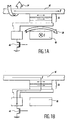
- les figures 1A et 1B, déjà décrites, montrent un dispositif connu pour l'écriture et la lecture d'une information binaire dans une jonction magnétique à effet tunnel par des champs magnétiques extérieurs ;
- la figure 2 montre, en coupe, un premier mode de réalisation d'un dispositif selon l'invention ;
- les figures 3A et 3B montrent les orientations des aimantations dans les différentes couches selon qu'on a écrit un "0" ou un "1" pour ce premier mode de réalisation ;
- les figures 4A et 4B montrent les variations transitoires de la composante de l'aimantation selon un axe Oz perpendiculaire au plan des couches et selon un axe Oy parallèle au plan des couches, pour une faible et une forte anisotropie ;
- la figure 5 montre, en coupe, un second mode de réalisation d'un dispositif selon l'invention ;
- les figures 6A et 6B montrent les orientations des aimantations dans les différentes couches selon qu'on a écrit un "O" ou un "1", pour ce second mode de réalisation ;
- la figure 7 montre schématiquement une mémoire utilisant une matrice de dispositifs selon l'invention.
- t est l'épaisseur de la couche magnétique à retourner,
- Ms est l'aimantation à saturation de la couche à retourner, dans le cas de CoFe (Ms=1500 emu/cc)),
- Hk est l'anisotropie de la couche magnétique à retourner,
- Jc (écriture) est la densité de courant pour écrire un point mémoire,
- RAmax est le produit de la résistance par la surface de la jonction tunnel, défini de telle façon que la tension à l'écriture n'excède pas 0,6 V,
- Jc (lecture) est la densité de courant pour une tension de lecture de 0,3 V avec RAmax,
- amin est la taille minimale d'un côté du point mémoire (pour un point mémoire carré) avant d'atteindre la limite superparamagnétique.
| Mode de réalisation | 1 | 2 |
| t(nm) | 5 | 5 |
| Ms (emu/cc) | 1500 | 1500 |
| Hk effectif (G) | 40 | 40 |
| Jc (écriture) (A/cm2) | 3,2E + 05 | 1,6E + 05 |
| RAmax (Ohm.µm2) | 188 | 375 |
| Jc (lecture) (A/cm2) | 1,6E + 05 | 8E + 04 |
| amin (micron) | 0,12 | 0,12 |
Claims (11)
- Dispositif magnétique comprenant :caractérisé en ce que la couche magnétique libre (16), au moins, est formée d'un premier empilement tri-couche constitué par deux couches magnétiques (161, 163) à aimantations antiparallèles séparées par une couche conductrice non magnétique (162).une première couche magnétique dite "piégée" (12) ayant une aimantation de direction fixe,une seconde couche magnétique dite "libre" (16) ayant une aimantation de direction variable,une couche isolante ou semi-conductrice (14) séparant la couche piégée et la couche libre,des moyens (22, 24) pour faire circuler dans les couches et perpendiculairement à celles-ci un courant d'électrons,des moyens de polarisation du spin de ces électrons,
- Dispositif selon la revendication 1, dans lequel ladite couche magnétique piégée (12) est formée d'un deuxième empilement tri-couche constitué par deux couches magnétiques (121, 123) d'aimantations antiparallèles séparées par une couche conductrice non magnétique (122), ce deuxième empilement étant recouvert d'une première couche d'échange antiferromagnétique (10) fixant la direction des aimantations dans ledit deuxième empilement tri-couche (12).
- Dispositif selon la revendication 2, comprenant en outre un troisième empilement tri-couche formé (32) par deux couches magnétiques (321, 323) à aimantations antiparallèles séparées par une couche conductrice non magnétique (322), ce troisième empilement tri-couche (32) étant séparé du premier (16) par une couche conductrice non magnétique (30), ce troisième empilement tri-couche (32) reposant sur une seconde couche d'échange antiferromagnétique (34) fixant les aimantations dans ledit troisième empilement tri-couche (32).
- Dispositif selon l'une quelconque des revendications 1 à 3, dans lequel les deux couches magnétiques (161, 163) du premier empilement tri-couche (16) ont même épaisseur.
- Dispositif selon l'une quelconque des revendications 1 à 3, dans lequel les couches magnétiques du premier (16) et/ou du deuxième (12) et/ou du troisième (32) empilement tri-couche sont en un matériau pris dans le groupe constitué par Co, Fe, Ni et leurs alliages.
- Dispositif selon l'une quelconque des revendications 1 à 3, dans lequel la couche conductrice non magnétique du premier (162) et/ou du deuxième (122) et/ou du troisième (322) empilement tri-couche est en un métal pris dans le groupe constitué par Ru, Re, Cu, Cr, Pt, Ag.
- Dispositif selon l'une quelconque des revendications 2 et 3, dans lequel la première (10) et/ou la seconde (34) couche antiferromagnétique est en alliage à base de Mn.
- Dispositif selon l'une quelconque des revendications 1 à 7, comprenant en outre des moyens d'écriture aptes à faire circuler un courant d'électrons à travers les couches dans un sens ou dans le sens opposé, ce courant ayant une densité supérieure à une certaine densité critique.
- Dispositif selon la revendication 8, comprenant en outre des moyens de lecture aptes à faire circuler un courant d'électrons à travers les couches avec une densité inférieure à ladite densité critique, et des moyens pour mesurer la tension apparaissant aux bornes de l'empilement de couches.
- Mémoire comprenant une matrice de points mémoire adressables par des lignes (80) et des colonnes d'adressage (90), caractérisée en ce que chaque point mémoire est constitué par un dispositif magnétique (60) selon l'une quelconque des revendications 1 à 7, et par un moyen de commutation de courant (70) placé en série avec le dispositif (60), chaque dispositif magnétique (60) étant relié à une ligne d'adressage (80) et chaque moyen de commutation (70) à une colonne d'adressage (90).
- Mémoire selon la revendication 10, comprenant en outre une colonne de référence (100) et des moyens pour comparer la tension lue aux bornes d'un dispositif situé au croisement d'une ligne (80) et d'une colonne (96) déterminées et la tension lue aux bornes du dispositif située sur la même ligne (80) mais sur la colonne de référence (100).
Applications Claiming Priority (2)
| Application Number | Priority Date | Filing Date | Title |
|---|---|---|---|
| FR0015895 | 2000-12-07 | ||
| FR0015895A FR2817999B1 (fr) | 2000-12-07 | 2000-12-07 | Dispositif magnetique a polarisation de spin et a empilement(s) tri-couche(s) et memoire utilisant ce dispositif |
Publications (2)
| Publication Number | Publication Date |
|---|---|
| EP1223585A1 true EP1223585A1 (fr) | 2002-07-17 |
| EP1223585B1 EP1223585B1 (fr) | 2008-04-16 |
Family
ID=8857352
Family Applications (1)
| Application Number | Title | Priority Date | Filing Date |
|---|---|---|---|
| EP01403132A Expired - Lifetime EP1223585B1 (fr) | 2000-12-07 | 2001-12-05 | Dispositif magnétique à polarisation de spin et à empilement(s) tri-couche(s) et mémoire utilisant ce dispositif |
Country Status (5)
| Country | Link |
|---|---|
| US (1) | US6603677B2 (fr) |
| EP (1) | EP1223585B1 (fr) |
| JP (2) | JP4398127B2 (fr) |
| DE (1) | DE60133622T2 (fr) |
| FR (1) | FR2817999B1 (fr) |
Cited By (2)
| Publication number | Priority date | Publication date | Assignee | Title |
|---|---|---|---|---|
| WO2004038723A2 (fr) * | 2002-10-22 | 2004-05-06 | Btg International Limited | Memoire magnetique |
| EP1418620A2 (fr) * | 2002-11-07 | 2004-05-12 | Samsung Electronics Co., Ltd. | MRAM et ses procédés de fabrication et de commande |
Families Citing this family (298)
| Publication number | Priority date | Publication date | Assignee | Title |
|---|---|---|---|---|
| JPS6093175A (ja) * | 1983-10-27 | 1985-05-24 | Nippon Denso Co Ltd | 燃料噴射時期調整装置の噴射時期検出装置 |
| DE10059181C2 (de) * | 2000-11-29 | 2002-10-24 | Infineon Technologies Ag | Integrierter magnetoresistiver Halbleiterspeicher und Herstellungsverfahren dafür |
| US6785092B2 (en) * | 2001-07-24 | 2004-08-31 | Seagate Technology Llc | White head for high anisotropy media |
| JP4780878B2 (ja) * | 2001-08-02 | 2011-09-28 | ルネサスエレクトロニクス株式会社 | 薄膜磁性体記憶装置 |
| FR2832542B1 (fr) | 2001-11-16 | 2005-05-06 | Commissariat Energie Atomique | Dispositif magnetique a jonction tunnel magnetique, memoire et procedes d'ecriture et de lecture utilisant ce dispositif |
| JP3866567B2 (ja) * | 2001-12-13 | 2007-01-10 | 株式会社東芝 | 半導体記憶装置及びその製造方法 |
| JP3583102B2 (ja) * | 2001-12-27 | 2004-10-27 | 株式会社東芝 | 磁気スイッチング素子及び磁気メモリ |
| US6606262B2 (en) * | 2002-01-10 | 2003-08-12 | Hewlett-Packard Development Company, L.P. | Magnetoresistive random access memory (MRAM) with on-chip automatic determination of optimized write current method and apparatus |
| US6714444B2 (en) * | 2002-08-06 | 2004-03-30 | Grandis, Inc. | Magnetic element utilizing spin transfer and an MRAM device using the magnetic element |
| JP4146202B2 (ja) * | 2002-09-24 | 2008-09-10 | 株式会社東芝 | スピントンネルトランジスタ、磁気再生ヘッド、磁気情報再生システム、及び磁気記憶装置 |
| US6838740B2 (en) * | 2002-09-27 | 2005-01-04 | Grandis, Inc. | Thermally stable magnetic elements utilizing spin transfer and an MRAM device using the magnetic element |
| US6958927B1 (en) | 2002-10-09 | 2005-10-25 | Grandis Inc. | Magnetic element utilizing spin-transfer and half-metals and an MRAM device using the magnetic element |
| JP4102280B2 (ja) * | 2002-10-14 | 2008-06-18 | 三星電子株式会社 | スピン分極電子を用いた磁性媒体及び磁性媒体への情報記録装置及び記録方法 |
| US6791867B2 (en) * | 2002-11-18 | 2004-09-14 | Hewlett-Packard Development Company, L.P. | Selection of memory cells in data storage devices |
| CN100533589C (zh) * | 2002-11-26 | 2009-08-26 | 株式会社东芝 | 磁单元和磁存储器 |
| JP2004179483A (ja) * | 2002-11-28 | 2004-06-24 | Hitachi Ltd | 不揮発性磁気メモリ |
| JP4873338B2 (ja) * | 2002-12-13 | 2012-02-08 | 独立行政法人科学技術振興機構 | スピン注入デバイス及びこれを用いた磁気装置 |
| JP2011171756A (ja) * | 2002-12-13 | 2011-09-01 | Japan Science & Technology Agency | スピン注入デバイス及びこれを用いた磁気装置 |
| US7190611B2 (en) * | 2003-01-07 | 2007-03-13 | Grandis, Inc. | Spin-transfer multilayer stack containing magnetic layers with resettable magnetization |
| US6829161B2 (en) * | 2003-01-10 | 2004-12-07 | Grandis, Inc. | Magnetostatically coupled magnetic elements utilizing spin transfer and an MRAM device using the magnetic element |
| US6847547B2 (en) * | 2003-02-28 | 2005-01-25 | Grandis, Inc. | Magnetostatically coupled magnetic elements utilizing spin transfer and an MRAM device using the magnetic element |
| US6952364B2 (en) * | 2003-03-03 | 2005-10-04 | Samsung Electronics Co., Ltd. | Magnetic tunnel junction structures and methods of fabrication |
| KR100615600B1 (ko) * | 2004-08-09 | 2006-08-25 | 삼성전자주식회사 | 고집적 자기램 소자 및 그 제조방법 |
| KR100542743B1 (ko) * | 2003-04-22 | 2006-01-11 | 삼성전자주식회사 | 자기 랜덤 엑세스 메모리 |
| US6933155B2 (en) * | 2003-05-21 | 2005-08-23 | Grandis, Inc. | Methods for providing a sub .15 micron magnetic memory structure |
| US6865109B2 (en) * | 2003-06-06 | 2005-03-08 | Seagate Technology Llc | Magnetic random access memory having flux closure for the free layer and spin transfer write mechanism |
| US7006375B2 (en) * | 2003-06-06 | 2006-02-28 | Seagate Technology Llc | Hybrid write mechanism for high speed and high density magnetic random access memory |
| JP4966483B2 (ja) * | 2003-06-25 | 2012-07-04 | パナソニック株式会社 | 磁気抵抗効果素子、および磁気抵抗効果素子を用いた磁気ヘッド、記録再生装置、メモリ素子、メモリアレイ、および磁気抵抗効果素子の製造方法 |
| JP2005064050A (ja) * | 2003-08-14 | 2005-03-10 | Toshiba Corp | 半導体記憶装置及びそのデータ書き込み方法 |
| US7573737B2 (en) * | 2003-08-19 | 2009-08-11 | New York University | High speed low power magnetic devices based on current induced spin-momentum transfer |
| US7911832B2 (en) | 2003-08-19 | 2011-03-22 | New York University | High speed low power magnetic devices based on current induced spin-momentum transfer |
| US6980469B2 (en) * | 2003-08-19 | 2005-12-27 | New York University | High speed low power magnetic devices based on current induced spin-momentum transfer |
| US8755222B2 (en) | 2003-08-19 | 2014-06-17 | New York University | Bipolar spin-transfer switching |
| US6985385B2 (en) | 2003-08-26 | 2006-01-10 | Grandis, Inc. | Magnetic memory element utilizing spin transfer switching and storing multiple bits |
| JP2005093488A (ja) * | 2003-09-12 | 2005-04-07 | Sony Corp | 磁気抵抗効果素子とその製造方法、および磁気メモリ装置とその製造方法 |
| US7161829B2 (en) * | 2003-09-19 | 2007-01-09 | Grandis, Inc. | Current confined pass layer for magnetic elements utilizing spin-transfer and an MRAM device using such magnetic elements |
| KR100615089B1 (ko) * | 2004-07-14 | 2006-08-23 | 삼성전자주식회사 | 낮은 구동 전류를 갖는 자기 램 |
| US7372722B2 (en) * | 2003-09-29 | 2008-05-13 | Samsung Electronics Co., Ltd. | Methods of operating magnetic random access memory devices including heat-generating structures |
| US7369428B2 (en) * | 2003-09-29 | 2008-05-06 | Samsung Electronics Co., Ltd. | Methods of operating a magnetic random access memory device and related devices and structures |
| KR100568512B1 (ko) * | 2003-09-29 | 2006-04-07 | 삼성전자주식회사 | 열발생층을 갖는 자기열 램셀들 및 이를 구동시키는 방법들 |
| KR100835275B1 (ko) * | 2004-08-12 | 2008-06-05 | 삼성전자주식회사 | 스핀 주입 메카니즘을 사용하여 자기램 소자를 구동시키는방법들 |
| JP2005109263A (ja) * | 2003-09-30 | 2005-04-21 | Toshiba Corp | 磁性体素子及磁気メモリ |
| US7027320B2 (en) * | 2003-10-21 | 2006-04-11 | Hewlett-Packard Development Company, L.P. | Soft-reference magnetic memory digitized device and method of operation |
| US7009877B1 (en) | 2003-11-14 | 2006-03-07 | Grandis, Inc. | Three-terminal magnetostatically coupled spin transfer-based MRAM cell |
| US7282755B2 (en) | 2003-11-14 | 2007-10-16 | Grandis, Inc. | Stress assisted current driven switching for magnetic memory applications |
| US7602000B2 (en) | 2003-11-19 | 2009-10-13 | International Business Machines Corporation | Spin-current switched magnetic memory element suitable for circuit integration and method of fabricating the memory element |
| JP2005166087A (ja) * | 2003-11-28 | 2005-06-23 | Toshiba Corp | 半導体集積回路装置 |
| JP4581394B2 (ja) * | 2003-12-22 | 2010-11-17 | ソニー株式会社 | 磁気メモリ |
| US20050136600A1 (en) * | 2003-12-22 | 2005-06-23 | Yiming Huai | Magnetic elements with ballistic magnetoresistance utilizing spin-transfer and an MRAM device using such magnetic elements |
| JP2005209248A (ja) * | 2004-01-20 | 2005-08-04 | Hitachi Ltd | 磁気ヘッド及び磁気記録再生装置 |
| US7110287B2 (en) | 2004-02-13 | 2006-09-19 | Grandis, Inc. | Method and system for providing heat assisted switching of a magnetic element utilizing spin transfer |
| US7242045B2 (en) | 2004-02-19 | 2007-07-10 | Grandis, Inc. | Spin transfer magnetic element having low saturation magnetization free layers |
| US6967863B2 (en) | 2004-02-25 | 2005-11-22 | Grandis, Inc. | Perpendicular magnetization magnetic element utilizing spin transfer |
| US6992359B2 (en) * | 2004-02-26 | 2006-01-31 | Grandis, Inc. | Spin transfer magnetic element with free layers having high perpendicular anisotropy and in-plane equilibrium magnetization |
| US20110140217A1 (en) * | 2004-02-26 | 2011-06-16 | Grandis, Inc. | Spin transfer magnetic element with free layers having high perpendicular anisotropy and in-plane equilibrium magnetization |
| JP2006148039A (ja) * | 2004-03-03 | 2006-06-08 | Toshiba Corp | 磁気抵抗効果素子および磁気メモリ |
| JP2005294376A (ja) | 2004-03-31 | 2005-10-20 | Toshiba Corp | 磁気記録素子及び磁気メモリ |
| US6946698B1 (en) | 2004-04-02 | 2005-09-20 | Taiwan Semiconductor Manufacturing Company, Ltd. | MRAM device having low-k inter-metal dielectric |
| JP4747507B2 (ja) * | 2004-04-16 | 2011-08-17 | ソニー株式会社 | 磁気メモリ及びその記録方法 |
| US7233039B2 (en) * | 2004-04-21 | 2007-06-19 | Grandis, Inc. | Spin transfer magnetic elements with spin depolarization layers |
| US7088609B2 (en) * | 2004-05-11 | 2006-08-08 | Grandis, Inc. | Spin barrier enhanced magnetoresistance effect element and magnetic memory using the same |
| US7057921B2 (en) * | 2004-05-11 | 2006-06-06 | Grandis, Inc. | Spin barrier enhanced dual magnetoresistance effect element and magnetic memory using the same |
| US7576956B2 (en) * | 2004-07-26 | 2009-08-18 | Grandis Inc. | Magnetic tunnel junction having diffusion stop layer |
| KR100660539B1 (ko) * | 2004-07-29 | 2006-12-22 | 삼성전자주식회사 | 자기 기억 소자 및 그 형성 방법 |
| US7221584B2 (en) * | 2004-08-13 | 2007-05-22 | Taiwan Semiconductor Manufacturing Company, Ltd. | MRAM cell having shared configuration |
| JP4568152B2 (ja) * | 2004-09-17 | 2010-10-27 | 株式会社東芝 | 磁気記録素子及びそれを用いた磁気記録装置 |
| JP4920881B2 (ja) * | 2004-09-27 | 2012-04-18 | 株式会社日立製作所 | 低消費電力磁気メモリ及び磁化情報書き込み装置 |
| JP2006108316A (ja) * | 2004-10-04 | 2006-04-20 | Sony Corp | 記憶素子及びメモリ |
| JP4626253B2 (ja) * | 2004-10-08 | 2011-02-02 | ソニー株式会社 | 記憶装置 |
| KR100642638B1 (ko) * | 2004-10-21 | 2006-11-10 | 삼성전자주식회사 | 낮은 임계 전류를 갖는 자기 램 소자의 구동 방법들 |
| US7149106B2 (en) * | 2004-10-22 | 2006-12-12 | Freescale Semiconductor, Inc. | Spin-transfer based MRAM using angular-dependent selectivity |
| US20060092688A1 (en) * | 2004-10-29 | 2006-05-04 | International Business Machines Corporation | Stacked magnetic devices |
| JP2006165264A (ja) * | 2004-12-07 | 2006-06-22 | Sony Corp | メモリ、磁気ヘッド及び磁気センサー、並びにこれらの製造方法 |
| JP2006179694A (ja) * | 2004-12-22 | 2006-07-06 | Sony Corp | 記憶素子 |
| US7170775B2 (en) * | 2005-01-06 | 2007-01-30 | Taiwan Semiconductor Manufacturing Company, Ltd. | MRAM cell with reduced write current |
| JP2007027197A (ja) * | 2005-07-12 | 2007-02-01 | Sony Corp | 記憶素子 |
| JP2007027575A (ja) * | 2005-07-20 | 2007-02-01 | Toshiba Corp | 磁気抵抗効果素子および磁気メモリ |
| JP5096702B2 (ja) * | 2005-07-28 | 2012-12-12 | 株式会社日立製作所 | 磁気抵抗効果素子及びそれを搭載した不揮発性磁気メモリ |
| US7224601B2 (en) | 2005-08-25 | 2007-05-29 | Grandis Inc. | Oscillating-field assisted spin torque switching of a magnetic tunnel junction memory element |
| JP2007081280A (ja) * | 2005-09-16 | 2007-03-29 | Fujitsu Ltd | 磁気抵抗効果素子及び磁気メモリ装置 |
| US7777261B2 (en) * | 2005-09-20 | 2010-08-17 | Grandis Inc. | Magnetic device having stabilized free ferromagnetic layer |
| US7859034B2 (en) * | 2005-09-20 | 2010-12-28 | Grandis Inc. | Magnetic devices having oxide antiferromagnetic layer next to free ferromagnetic layer |
| US7973349B2 (en) * | 2005-09-20 | 2011-07-05 | Grandis Inc. | Magnetic device having multilayered free ferromagnetic layer |
| JP5120699B2 (ja) * | 2005-10-03 | 2013-01-16 | 日本電気株式会社 | 磁気ランダムアクセスメモリ及びその動作方法 |
| US7286395B2 (en) * | 2005-10-27 | 2007-10-23 | Grandis, Inc. | Current driven switched magnetic storage cells having improved read and write margins and magnetic memories using such cells |
| FR2892871B1 (fr) * | 2005-11-02 | 2007-11-23 | Commissariat Energie Atomique | Oscillateur radio frequence a courant elelctrique polarise en spin |
| US7430135B2 (en) * | 2005-12-23 | 2008-09-30 | Grandis Inc. | Current-switched spin-transfer magnetic devices with reduced spin-transfer switching current density |
| US8058696B2 (en) * | 2006-02-25 | 2011-11-15 | Avalanche Technology, Inc. | High capacity low cost multi-state magnetic memory |
| US8084835B2 (en) * | 2006-10-20 | 2011-12-27 | Avalanche Technology, Inc. | Non-uniform switching based non-volatile magnetic based memory |
| US20080246104A1 (en) * | 2007-02-12 | 2008-10-09 | Yadav Technology | High Capacity Low Cost Multi-State Magnetic Memory |
| US8535952B2 (en) * | 2006-02-25 | 2013-09-17 | Avalanche Technology, Inc. | Method for manufacturing non-volatile magnetic memory |
| US20070253245A1 (en) * | 2006-04-27 | 2007-11-01 | Yadav Technology | High Capacity Low Cost Multi-Stacked Cross-Line Magnetic Memory |
| US8508984B2 (en) * | 2006-02-25 | 2013-08-13 | Avalanche Technology, Inc. | Low resistance high-TMR magnetic tunnel junction and process for fabrication thereof |
| US8063459B2 (en) * | 2007-02-12 | 2011-11-22 | Avalanche Technologies, Inc. | Non-volatile magnetic memory element with graded layer |
| US8018011B2 (en) * | 2007-02-12 | 2011-09-13 | Avalanche Technology, Inc. | Low cost multi-state magnetic memory |
| US8183652B2 (en) * | 2007-02-12 | 2012-05-22 | Avalanche Technology, Inc. | Non-volatile magnetic memory with low switching current and high thermal stability |
| US7732881B2 (en) * | 2006-11-01 | 2010-06-08 | Avalanche Technology, Inc. | Current-confined effect of magnetic nano-current-channel (NCC) for magnetic random access memory (MRAM) |
| US20070246787A1 (en) * | 2006-03-29 | 2007-10-25 | Lien-Chang Wang | On-plug magnetic tunnel junction devices based on spin torque transfer switching |
| JP2007273523A (ja) * | 2006-03-30 | 2007-10-18 | Tdk Corp | 磁気メモリ及びスピン注入方法 |
| JP4277870B2 (ja) * | 2006-04-17 | 2009-06-10 | ソニー株式会社 | 記憶素子及びメモリ |
| JP5096690B2 (ja) | 2006-04-26 | 2012-12-12 | 株式会社日立製作所 | 磁気メモリセル及びランダムアクセスメモリ |
| JP2007294737A (ja) | 2006-04-26 | 2007-11-08 | Hitachi Ltd | トンネル磁気抵抗効果素子、それを用いた磁気メモリセル及びランダムアクセスメモリ |
| DE602006013948D1 (de) * | 2006-05-04 | 2010-06-10 | Hitachi Ltd | Magnetspeichervorrichtung |
| JP2007305882A (ja) * | 2006-05-12 | 2007-11-22 | Sony Corp | 記憶素子及びメモリ |
| JP5076361B2 (ja) * | 2006-05-18 | 2012-11-21 | 株式会社日立製作所 | 半導体装置 |
| US7532505B1 (en) * | 2006-07-17 | 2009-05-12 | Grandis, Inc. | Method and system for using a pulsed field to assist spin transfer induced switching of magnetic memory elements |
| US7502249B1 (en) * | 2006-07-17 | 2009-03-10 | Grandis, Inc. | Method and system for using a pulsed field to assist spin transfer induced switching of magnetic memory elements |
| US7851840B2 (en) * | 2006-09-13 | 2010-12-14 | Grandis Inc. | Devices and circuits based on magnetic tunnel junctions utilizing a multilayer barrier |
| JP5147212B2 (ja) * | 2006-10-04 | 2013-02-20 | 株式会社日立製作所 | 磁気メモリセル及び磁気ランダムアクセスメモリ |
| TWI449040B (zh) | 2006-10-06 | 2014-08-11 | Crocus Technology Sa | 用於提供內容可定址的磁阻式隨機存取記憶體單元之系統及方法 |
| US7742329B2 (en) * | 2007-03-06 | 2010-06-22 | Qualcomm Incorporated | Word line transistor strength control for read and write in spin transfer torque magnetoresistive random access memory |
| JP4682998B2 (ja) * | 2007-03-15 | 2011-05-11 | ソニー株式会社 | 記憶素子及びメモリ |
| WO2008123023A1 (fr) * | 2007-03-16 | 2008-10-16 | Keio University | Procédé de changement/relaxation de spin, méthode de détection de courant de spin et dispositif spintronique faisant intervenir la relaxation de spin |
| US7573736B2 (en) * | 2007-05-22 | 2009-08-11 | Taiwan Semiconductor Manufacturing Company | Spin torque transfer MRAM device |
| JP4625936B2 (ja) * | 2007-06-12 | 2011-02-02 | 独立行政法人産業技術総合研究所 | 乱数発生器 |
| WO2008154519A1 (fr) * | 2007-06-12 | 2008-12-18 | Grandis, Inc. | Procédé et système pour produire un élément magnétique et une mémoire magnétique à écriture unidirectionnelle |
| US7688616B2 (en) * | 2007-06-18 | 2010-03-30 | Taiwan Semicondcutor Manufacturing Company, Ltd. | Device and method of programming a magnetic memory element |
| US7957179B2 (en) * | 2007-06-27 | 2011-06-07 | Grandis Inc. | Magnetic shielding in magnetic multilayer structures |
| FR2918762B1 (fr) * | 2007-07-10 | 2010-03-19 | Commissariat Energie Atomique | Capteur de champ magnetique a faible bruit utilisant un transfert de spin lateral. |
| FR2918761B1 (fr) * | 2007-07-10 | 2009-11-06 | Commissariat Energie Atomique | Capteur de champ magnetique a faible bruit. |
| JP4874884B2 (ja) | 2007-07-11 | 2012-02-15 | 株式会社東芝 | 磁気記録素子及び磁気記録装置 |
| US7982275B2 (en) | 2007-08-22 | 2011-07-19 | Grandis Inc. | Magnetic element having low saturation magnetization |
| US9812184B2 (en) | 2007-10-31 | 2017-11-07 | New York University | Current induced spin-momentum transfer stack with dual insulating layers |
| WO2009074411A1 (fr) | 2007-12-13 | 2009-06-18 | Crocus Technology | Mémoire magnétique à procédure d'écriture assistée thermiquement |
| JP2009158877A (ja) | 2007-12-28 | 2009-07-16 | Hitachi Ltd | 磁気メモリセル及びランダムアクセスメモリ |
| US8013406B2 (en) * | 2008-01-02 | 2011-09-06 | The Hong Kong University Of Science And Technology | Method and apparatus for generating giant spin-dependent chemical potential difference in non-magnetic materials |
| US7919794B2 (en) * | 2008-01-08 | 2011-04-05 | Qualcomm, Incorporated | Memory cell and method of forming a magnetic tunnel junction (MTJ) of a memory cell |
| JP5283922B2 (ja) * | 2008-02-14 | 2013-09-04 | 株式会社東芝 | 磁気メモリ |
| JP5455313B2 (ja) * | 2008-02-21 | 2014-03-26 | 株式会社東芝 | 磁気記憶素子及び磁気記憶装置 |
| US8802451B2 (en) | 2008-02-29 | 2014-08-12 | Avalanche Technology Inc. | Method for manufacturing high density non-volatile magnetic memory |
| EP2109111B1 (fr) | 2008-04-07 | 2011-12-21 | Crocus Technology S.A. | Système et procédé pour écrire des données sur des cellules à mémoire à accès aléatoire |
| US8659852B2 (en) | 2008-04-21 | 2014-02-25 | Seagate Technology Llc | Write-once magentic junction memory array |
| FR2931011B1 (fr) * | 2008-05-06 | 2010-05-28 | Commissariat Energie Atomique | Element magnetique a ecriture assistee thermiquement |
| EP2124228B1 (fr) | 2008-05-20 | 2014-03-05 | Crocus Technology | Mémoire à accès aléatoire magnétique avec une jonction elliptique |
| US7855911B2 (en) | 2008-05-23 | 2010-12-21 | Seagate Technology Llc | Reconfigurable magnetic logic device using spin torque |
| JP5339272B2 (ja) | 2008-06-05 | 2013-11-13 | 国立大学法人東北大学 | スピントロニクスデバイス及び情報伝達方法 |
| US8031519B2 (en) | 2008-06-18 | 2011-10-04 | Crocus Technology S.A. | Shared line magnetic random access memory cells |
| US8274818B2 (en) | 2008-08-05 | 2012-09-25 | Tohoku University | Magnetoresistive element, magnetic memory cell and magnetic random access memory using the same |
| US7881098B2 (en) | 2008-08-26 | 2011-02-01 | Seagate Technology Llc | Memory with separate read and write paths |
| US7894248B2 (en) * | 2008-09-12 | 2011-02-22 | Grandis Inc. | Programmable and redundant circuitry based on magnetic tunnel junction (MTJ) |
| US8189370B2 (en) * | 2008-09-22 | 2012-05-29 | Hitachi, Ltd. | Magnetic recording element, magnetic memory cell, and magnetic random access memory |
| US7985994B2 (en) | 2008-09-29 | 2011-07-26 | Seagate Technology Llc | Flux-closed STRAM with electronically reflective insulative spacer |
| US8169810B2 (en) | 2008-10-08 | 2012-05-01 | Seagate Technology Llc | Magnetic memory with asymmetric energy barrier |
| US8089132B2 (en) * | 2008-10-09 | 2012-01-03 | Seagate Technology Llc | Magnetic memory with phonon glass electron crystal material |
| US8039913B2 (en) | 2008-10-09 | 2011-10-18 | Seagate Technology Llc | Magnetic stack with laminated layer |
| US7880209B2 (en) * | 2008-10-09 | 2011-02-01 | Seagate Technology Llc | MRAM cells including coupled free ferromagnetic layers for stabilization |
| US8228703B2 (en) | 2008-11-04 | 2012-07-24 | Crocus Technology Sa | Ternary Content Addressable Magnetoresistive random access memory cell |
| US8043732B2 (en) | 2008-11-11 | 2011-10-25 | Seagate Technology Llc | Memory cell with radial barrier |
| US7826181B2 (en) | 2008-11-12 | 2010-11-02 | Seagate Technology Llc | Magnetic memory with porous non-conductive current confinement layer |
| US8743593B2 (en) * | 2008-12-10 | 2014-06-03 | Hitachi, Ltd. | Magnetoresistance effect element and magnetic memory cell and magnetic random access memory using same |
| US8344433B2 (en) * | 2009-04-14 | 2013-01-01 | Qualcomm Incorporated | Magnetic tunnel junction (MTJ) and methods, and magnetic random access memory (MRAM) employing same |
| EP2249349B1 (fr) * | 2009-05-08 | 2012-02-08 | Crocus Technology | Mémoire magnétique dotée d'une procédure d'écriture thermiquement assistée et d'un champ d'écriture réduit |
| ATE544153T1 (de) * | 2009-05-08 | 2012-02-15 | Crocus Technology | Magnetischer speicher mit wärmeunterstütztem schreibverfahren und niedrigem schreibstrom |
| US8218349B2 (en) | 2009-05-26 | 2012-07-10 | Crocus Technology Sa | Non-volatile logic devices using magnetic tunnel junctions |
| US7999338B2 (en) | 2009-07-13 | 2011-08-16 | Seagate Technology Llc | Magnetic stack having reference layers with orthogonal magnetization orientation directions |
| US8102703B2 (en) | 2009-07-14 | 2012-01-24 | Crocus Technology | Magnetic element with a fast spin transfer torque writing procedure |
| US20110031569A1 (en) * | 2009-08-10 | 2011-02-10 | Grandis, Inc. | Method and system for providing magnetic tunneling junction elements having improved performance through capping layer induced perpendicular anisotropy and memories using such magnetic elements |
| US10446209B2 (en) * | 2009-08-10 | 2019-10-15 | Samsung Semiconductor Inc. | Method and system for providing magnetic tunneling junction elements having improved performance through capping layer induced perpendicular anisotropy and memories using such magnetic elements |
| US8913350B2 (en) * | 2009-08-10 | 2014-12-16 | Grandis, Inc. | Method and system for providing magnetic tunneling junction elements having improved performance through capping layer induced perpendicular anisotropy and memories using such magnetic elements |
| US8385106B2 (en) * | 2009-09-11 | 2013-02-26 | Grandis, Inc. | Method and system for providing a hierarchical data path for spin transfer torque random access memory |
| US8159866B2 (en) | 2009-10-30 | 2012-04-17 | Grandis, Inc. | Method and system for providing dual magnetic tunneling junctions usable in spin transfer torque magnetic memories |
| US8422285B2 (en) * | 2009-10-30 | 2013-04-16 | Grandis, Inc. | Method and system for providing dual magnetic tunneling junctions usable in spin transfer torque magnetic memories |
| US20110141802A1 (en) * | 2009-12-15 | 2011-06-16 | Grandis, Inc. | Method and system for providing a high density memory cell for spin transfer torque random access memory |
| US8199553B2 (en) * | 2009-12-17 | 2012-06-12 | Hitachi Global Storage Technologies Netherlands B.V. | Multilevel frequency addressable field driven MRAM |
| US8063460B2 (en) * | 2009-12-18 | 2011-11-22 | Intel Corporation | Spin torque magnetic integrated circuits and devices therefor |
| US8254162B2 (en) | 2010-01-11 | 2012-08-28 | Grandis, Inc. | Method and system for providing magnetic tunneling junctions usable in spin transfer torque magnetic memories |
| US9130151B2 (en) | 2010-01-11 | 2015-09-08 | Samsung Electronics Co., Ltd. | Method and system for providing magnetic tunneling junctions usable in spin transfer torque magnetic memories |
| JP4903277B2 (ja) | 2010-01-26 | 2012-03-28 | 株式会社日立製作所 | 磁気抵抗効果素子、それを用いた磁気メモリセル及びランダムアクセスメモリ |
| JP5461683B2 (ja) * | 2010-03-05 | 2014-04-02 | 株式会社日立製作所 | 磁気メモリセル及び磁気ランダムアクセスメモリ |
| US8891290B2 (en) | 2010-03-17 | 2014-11-18 | Samsung Electronics Co., Ltd. | Method and system for providing inverted dual magnetic tunneling junction elements |
| US8411497B2 (en) | 2010-05-05 | 2013-04-02 | Grandis, Inc. | Method and system for providing a magnetic field aligned spin transfer torque random access memory |
| US8546896B2 (en) | 2010-07-16 | 2013-10-01 | Grandis, Inc. | Magnetic tunneling junction elements having magnetic substructures(s) with a perpendicular anisotropy and memories using such magnetic elements |
| US8374048B2 (en) | 2010-08-11 | 2013-02-12 | Grandis, Inc. | Method and system for providing magnetic tunneling junction elements having a biaxial anisotropy |
| FR2964248B1 (fr) | 2010-09-01 | 2013-07-19 | Commissariat Energie Atomique | Dispositif magnetique et procede de lecture et d’ecriture dans un tel dispositif magnetique |
| JP5742142B2 (ja) * | 2010-09-08 | 2015-07-01 | ソニー株式会社 | 記憶素子、メモリ装置 |
| FR2965654B1 (fr) | 2010-10-01 | 2012-10-19 | Commissariat Energie Atomique | Dispositif magnetique a ecriture assistee thermiquement |
| US8399941B2 (en) | 2010-11-05 | 2013-03-19 | Grandis, Inc. | Magnetic junction elements having an easy cone anisotropy and a magnetic memory using such magnetic junction elements |
| US8796794B2 (en) | 2010-12-17 | 2014-08-05 | Intel Corporation | Write current reduction in spin transfer torque memory devices |
| US8432009B2 (en) | 2010-12-31 | 2013-04-30 | Grandis, Inc. | Method and system for providing magnetic layers having insertion layers for use in spin transfer torque memories |
| US9478730B2 (en) | 2010-12-31 | 2016-10-25 | Samsung Electronics Co., Ltd. | Method and system for providing magnetic layers having insertion layers for use in spin transfer torque memories |
| EP2477227B1 (fr) | 2011-01-13 | 2019-03-27 | Crocus Technology S.A. | Jonction à effet tunnel magnétique avec une couche polarisante |
| JP5686626B2 (ja) * | 2011-02-22 | 2015-03-18 | ルネサスエレクトロニクス株式会社 | 磁気メモリ及びその製造方法 |
| FR2976113B1 (fr) | 2011-06-06 | 2013-07-12 | Commissariat Energie Atomique | Dispositif magnetique a couplage d'echange |
| FR2976396B1 (fr) | 2011-06-07 | 2013-07-12 | Commissariat Energie Atomique | Empilement magnetique et point memoire comportant un tel empilement |
| US8766383B2 (en) | 2011-07-07 | 2014-07-01 | Samsung Electronics Co., Ltd. | Method and system for providing a magnetic junction using half metallic ferromagnets |
| JP2012028798A (ja) * | 2011-09-14 | 2012-02-09 | Sony Corp | メモリ |
| US8570792B2 (en) * | 2012-01-24 | 2013-10-29 | Taiwan Semiconductor Manufacturing Co., Ltd. | Magnetoresistive random access memory |
| US8884386B2 (en) | 2012-02-02 | 2014-11-11 | Taiwan Semiconductor Manufacturing Company, Ltd. | MRAM device and fabrication method thereof |
| US9007818B2 (en) | 2012-03-22 | 2015-04-14 | Micron Technology, Inc. | Memory cells, semiconductor device structures, systems including such cells, and methods of fabrication |
| FR2989211B1 (fr) | 2012-04-10 | 2014-09-26 | Commissariat Energie Atomique | Dispositif magnetique a ecriture assistee thermiquement |
| US9054030B2 (en) | 2012-06-19 | 2015-06-09 | Micron Technology, Inc. | Memory cells, semiconductor device structures, memory systems, and methods of fabrication |
| US8923038B2 (en) | 2012-06-19 | 2014-12-30 | Micron Technology, Inc. | Memory cells, semiconductor device structures, memory systems, and methods of fabrication |
| FR2993387B1 (fr) | 2012-07-11 | 2014-08-08 | Commissariat Energie Atomique | Dispositif magnetique a ecriture assistee thermiquement |
| US9082888B2 (en) | 2012-10-17 | 2015-07-14 | New York University | Inverted orthogonal spin transfer layer stack |
| US9082950B2 (en) | 2012-10-17 | 2015-07-14 | New York University | Increased magnetoresistance in an inverted orthogonal spin transfer layer stack |
| US8879205B2 (en) | 2012-11-13 | 2014-11-04 | HGST Netherlands B.V. | High spin-torque efficiency spin-torque oscillator (STO) with dual spin polarization layer |
| KR102199622B1 (ko) * | 2013-01-11 | 2021-01-08 | 삼성전자주식회사 | 용이 콘 이방성을 가지는 자기 터널 접합 소자들을 제공하는 방법 및 시스템 |
| US9379315B2 (en) | 2013-03-12 | 2016-06-28 | Micron Technology, Inc. | Memory cells, methods of fabrication, semiconductor device structures, and memory systems |
| US9602103B2 (en) * | 2013-05-22 | 2017-03-21 | Hitachi, Ltd. | Spin wave device and logic circuit using spin wave device |
| US8982613B2 (en) | 2013-06-17 | 2015-03-17 | New York University | Scalable orthogonal spin transfer magnetic random access memory devices with reduced write error rates |
| US9368714B2 (en) | 2013-07-01 | 2016-06-14 | Micron Technology, Inc. | Memory cells, methods of operation and fabrication, semiconductor device structures, and memory systems |
| US9466787B2 (en) | 2013-07-23 | 2016-10-11 | Micron Technology, Inc. | Memory cells, methods of fabrication, semiconductor device structures, memory systems, and electronic systems |
| US9461242B2 (en) | 2013-09-13 | 2016-10-04 | Micron Technology, Inc. | Magnetic memory cells, methods of fabrication, semiconductor devices, memory systems, and electronic systems |
| US9608197B2 (en) | 2013-09-18 | 2017-03-28 | Micron Technology, Inc. | Memory cells, methods of fabrication, and semiconductor devices |
| US9529060B2 (en) | 2014-01-09 | 2016-12-27 | Allegro Microsystems, Llc | Magnetoresistance element with improved response to magnetic fields |
| US10454024B2 (en) | 2014-02-28 | 2019-10-22 | Micron Technology, Inc. | Memory cells, methods of fabrication, and memory devices |
| US9281466B2 (en) | 2014-04-09 | 2016-03-08 | Micron Technology, Inc. | Memory cells, semiconductor structures, semiconductor devices, and methods of fabrication |
| US9269888B2 (en) | 2014-04-18 | 2016-02-23 | Micron Technology, Inc. | Memory cells, methods of fabrication, and semiconductor devices |
| US9263667B1 (en) | 2014-07-25 | 2016-02-16 | Spin Transfer Technologies, Inc. | Method for manufacturing MTJ memory device |
| US9337412B2 (en) * | 2014-09-22 | 2016-05-10 | Spin Transfer Technologies, Inc. | Magnetic tunnel junction structure for MRAM device |
| US9349945B2 (en) | 2014-10-16 | 2016-05-24 | Micron Technology, Inc. | Memory cells, semiconductor devices, and methods of fabrication |
| US9768377B2 (en) | 2014-12-02 | 2017-09-19 | Micron Technology, Inc. | Magnetic cell structures, and methods of fabrication |
| US10439131B2 (en) | 2015-01-15 | 2019-10-08 | Micron Technology, Inc. | Methods of forming semiconductor devices including tunnel barrier materials |
| US9502642B2 (en) | 2015-04-10 | 2016-11-22 | Micron Technology, Inc. | Magnetic tunnel junctions, methods used while forming magnetic tunnel junctions, and methods of forming magnetic tunnel junctions |
| US9530959B2 (en) | 2015-04-15 | 2016-12-27 | Micron Technology, Inc. | Magnetic tunnel junctions |
| US9520553B2 (en) | 2015-04-15 | 2016-12-13 | Micron Technology, Inc. | Methods of forming a magnetic electrode of a magnetic tunnel junction and methods of forming a magnetic tunnel junction |
| US10468590B2 (en) | 2015-04-21 | 2019-11-05 | Spin Memory, Inc. | High annealing temperature perpendicular magnetic anisotropy structure for magnetic random access memory |
| US9728712B2 (en) | 2015-04-21 | 2017-08-08 | Spin Transfer Technologies, Inc. | Spin transfer torque structure for MRAM devices having a spin current injection capping layer |
| US9257136B1 (en) | 2015-05-05 | 2016-02-09 | Micron Technology, Inc. | Magnetic tunnel junctions |
| US9960346B2 (en) | 2015-05-07 | 2018-05-01 | Micron Technology, Inc. | Magnetic tunnel junctions |
| EP3300534B1 (fr) | 2015-06-05 | 2020-11-11 | Allegro MicroSystems, LLC | Élément de magnétorésistance à vanne de spin à réponse améliorée aux champs magnétiques |
| US9853206B2 (en) | 2015-06-16 | 2017-12-26 | Spin Transfer Technologies, Inc. | Precessional spin current structure for MRAM |
| US9773974B2 (en) | 2015-07-30 | 2017-09-26 | Spin Transfer Technologies, Inc. | Polishing stop layer(s) for processing arrays of semiconductor elements |
| US10163479B2 (en) | 2015-08-14 | 2018-12-25 | Spin Transfer Technologies, Inc. | Method and apparatus for bipolar memory write-verify |
| US10573363B2 (en) | 2015-12-02 | 2020-02-25 | Samsung Electronics Co., Ltd. | Method and apparatus for performing self-referenced read in a magnetoresistive random access memory |
| US9741926B1 (en) | 2016-01-28 | 2017-08-22 | Spin Transfer Technologies, Inc. | Memory cell having magnetic tunnel junction and thermal stability enhancement layer |
| JP2017139399A (ja) * | 2016-02-05 | 2017-08-10 | Tdk株式会社 | 磁気メモリ |
| US9680089B1 (en) | 2016-05-13 | 2017-06-13 | Micron Technology, Inc. | Magnetic tunnel junctions |
| US10546625B2 (en) | 2016-09-27 | 2020-01-28 | Spin Memory, Inc. | Method of optimizing write voltage based on error buffer occupancy |
| US11119910B2 (en) | 2016-09-27 | 2021-09-14 | Spin Memory, Inc. | Heuristics for selecting subsegments for entry in and entry out operations in an error cache system with coarse and fine grain segments |
| US10360964B2 (en) | 2016-09-27 | 2019-07-23 | Spin Memory, Inc. | Method of writing contents in memory during a power up sequence using a dynamic redundancy register in a memory device |
| US10460781B2 (en) | 2016-09-27 | 2019-10-29 | Spin Memory, Inc. | Memory device with a dual Y-multiplexer structure for performing two simultaneous operations on the same row of a memory bank |
| US10437723B2 (en) | 2016-09-27 | 2019-10-08 | Spin Memory, Inc. | Method of flushing the contents of a dynamic redundancy register to a secure storage area during a power down in a memory device |
| US10366774B2 (en) | 2016-09-27 | 2019-07-30 | Spin Memory, Inc. | Device with dynamic redundancy registers |
| US10991410B2 (en) | 2016-09-27 | 2021-04-27 | Spin Memory, Inc. | Bi-polar write scheme |
| US11151042B2 (en) | 2016-09-27 | 2021-10-19 | Integrated Silicon Solution, (Cayman) Inc. | Error cache segmentation for power reduction |
| US11119936B2 (en) | 2016-09-27 | 2021-09-14 | Spin Memory, Inc. | Error cache system with coarse and fine segments for power optimization |
| US10818331B2 (en) | 2016-09-27 | 2020-10-27 | Spin Memory, Inc. | Multi-chip module for MRAM devices with levels of dynamic redundancy registers |
| US10628316B2 (en) | 2016-09-27 | 2020-04-21 | Spin Memory, Inc. | Memory device with a plurality of memory banks where each memory bank is associated with a corresponding memory instruction pipeline and a dynamic redundancy register |
| US10446210B2 (en) | 2016-09-27 | 2019-10-15 | Spin Memory, Inc. | Memory instruction pipeline with a pre-read stage for a write operation for reducing power consumption in a memory device that uses dynamic redundancy registers |
| US10437491B2 (en) | 2016-09-27 | 2019-10-08 | Spin Memory, Inc. | Method of processing incomplete memory operations in a memory device during a power up sequence and a power down sequence using a dynamic redundancy register |
| US10672976B2 (en) | 2017-02-28 | 2020-06-02 | Spin Memory, Inc. | Precessional spin current structure with high in-plane magnetization for MRAM |
| US10665777B2 (en) | 2017-02-28 | 2020-05-26 | Spin Memory, Inc. | Precessional spin current structure with non-magnetic insertion layer for MRAM |
| US11022661B2 (en) | 2017-05-19 | 2021-06-01 | Allegro Microsystems, Llc | Magnetoresistance element with increased operational range |
| US10620279B2 (en) | 2017-05-19 | 2020-04-14 | Allegro Microsystems, Llc | Magnetoresistance element with increased operational range |
| US10032978B1 (en) | 2017-06-27 | 2018-07-24 | Spin Transfer Technologies, Inc. | MRAM with reduced stray magnetic fields |
| US10656994B2 (en) | 2017-10-24 | 2020-05-19 | Spin Memory, Inc. | Over-voltage write operation of tunnel magnet-resistance (“TMR”) memory device and correcting failure bits therefrom by using on-the-fly bit failure detection and bit redundancy remapping techniques |
| US10481976B2 (en) | 2017-10-24 | 2019-11-19 | Spin Memory, Inc. | Forcing bits as bad to widen the window between the distributions of acceptable high and low resistive bits thereby lowering the margin and increasing the speed of the sense amplifiers |
| US10489245B2 (en) | 2017-10-24 | 2019-11-26 | Spin Memory, Inc. | Forcing stuck bits, waterfall bits, shunt bits and low TMR bits to short during testing and using on-the-fly bit failure detection and bit redundancy remapping techniques to correct them |
| US10529439B2 (en) | 2017-10-24 | 2020-01-07 | Spin Memory, Inc. | On-the-fly bit failure detection and bit redundancy remapping techniques to correct for fixed bit defects |
| US10679685B2 (en) | 2017-12-27 | 2020-06-09 | Spin Memory, Inc. | Shared bit line array architecture for magnetoresistive memory |
| US10424726B2 (en) | 2017-12-28 | 2019-09-24 | Spin Memory, Inc. | Process for improving photoresist pillar adhesion during MRAM fabrication |
| US10360962B1 (en) | 2017-12-28 | 2019-07-23 | Spin Memory, Inc. | Memory array with individually trimmable sense amplifiers |
| US10891997B2 (en) | 2017-12-28 | 2021-01-12 | Spin Memory, Inc. | Memory array with horizontal source line and a virtual source line |
| US10395711B2 (en) | 2017-12-28 | 2019-08-27 | Spin Memory, Inc. | Perpendicular source and bit lines for an MRAM array |
| US10395712B2 (en) | 2017-12-28 | 2019-08-27 | Spin Memory, Inc. | Memory array with horizontal source line and sacrificial bitline per virtual source |
| US10516094B2 (en) | 2017-12-28 | 2019-12-24 | Spin Memory, Inc. | Process for creating dense pillars using multiple exposures for MRAM fabrication |
| US10811594B2 (en) | 2017-12-28 | 2020-10-20 | Spin Memory, Inc. | Process for hard mask development for MRAM pillar formation using photolithography |
| US10546624B2 (en) | 2017-12-29 | 2020-01-28 | Spin Memory, Inc. | Multi-port random access memory |
| US10360961B1 (en) | 2017-12-29 | 2019-07-23 | Spin Memory, Inc. | AC current pre-charge write-assist in orthogonal STT-MRAM |
| US10367139B2 (en) | 2017-12-29 | 2019-07-30 | Spin Memory, Inc. | Methods of manufacturing magnetic tunnel junction devices |
| US10199083B1 (en) | 2017-12-29 | 2019-02-05 | Spin Transfer Technologies, Inc. | Three-terminal MRAM with ac write-assist for low read disturb |
| US10236048B1 (en) | 2017-12-29 | 2019-03-19 | Spin Memory, Inc. | AC current write-assist in orthogonal STT-MRAM |
| US10236047B1 (en) | 2017-12-29 | 2019-03-19 | Spin Memory, Inc. | Shared oscillator (STNO) for MRAM array write-assist in orthogonal STT-MRAM |
| US10784439B2 (en) | 2017-12-29 | 2020-09-22 | Spin Memory, Inc. | Precessional spin current magnetic tunnel junction devices and methods of manufacture |
| US10270027B1 (en) | 2017-12-29 | 2019-04-23 | Spin Memory, Inc. | Self-generating AC current assist in orthogonal STT-MRAM |
| US10840439B2 (en) | 2017-12-29 | 2020-11-17 | Spin Memory, Inc. | Magnetic tunnel junction (MTJ) fabrication methods and systems |
| US10886330B2 (en) | 2017-12-29 | 2021-01-05 | Spin Memory, Inc. | Memory device having overlapping magnetic tunnel junctions in compliance with a reference pitch |
| US10840436B2 (en) | 2017-12-29 | 2020-11-17 | Spin Memory, Inc. | Perpendicular magnetic anisotropy interface tunnel junction devices and methods of manufacture |
| US10424723B2 (en) | 2017-12-29 | 2019-09-24 | Spin Memory, Inc. | Magnetic tunnel junction devices including an optimization layer |
| US10255962B1 (en) | 2017-12-30 | 2019-04-09 | Spin Memory, Inc. | Microwave write-assist in orthogonal STT-MRAM |
| US10319900B1 (en) | 2017-12-30 | 2019-06-11 | Spin Memory, Inc. | Perpendicular magnetic tunnel junction device with precessional spin current layer having a modulated moment density |
| US10141499B1 (en) | 2017-12-30 | 2018-11-27 | Spin Transfer Technologies, Inc. | Perpendicular magnetic tunnel junction device with offset precessional spin current layer |
| US10236439B1 (en) | 2017-12-30 | 2019-03-19 | Spin Memory, Inc. | Switching and stability control for perpendicular magnetic tunnel junction device |
| US10229724B1 (en) | 2017-12-30 | 2019-03-12 | Spin Memory, Inc. | Microwave write-assist in series-interconnected orthogonal STT-MRAM devices |
| US10339993B1 (en) | 2017-12-30 | 2019-07-02 | Spin Memory, Inc. | Perpendicular magnetic tunnel junction device with skyrmionic assist layers for free layer switching |
| US10468588B2 (en) | 2018-01-05 | 2019-11-05 | Spin Memory, Inc. | Perpendicular magnetic tunnel junction device with skyrmionic enhancement layers for the precessional spin current magnetic layer |
| US10438996B2 (en) | 2018-01-08 | 2019-10-08 | Spin Memory, Inc. | Methods of fabricating magnetic tunnel junctions integrated with selectors |
| US10438995B2 (en) | 2018-01-08 | 2019-10-08 | Spin Memory, Inc. | Devices including magnetic tunnel junctions integrated with selectors |
| US10446744B2 (en) | 2018-03-08 | 2019-10-15 | Spin Memory, Inc. | Magnetic tunnel junction wafer adaptor used in magnetic annealing furnace and method of using the same |
| US10388861B1 (en) | 2018-03-08 | 2019-08-20 | Spin Memory, Inc. | Magnetic tunnel junction wafer adaptor used in magnetic annealing furnace and method of using the same |
| US11107974B2 (en) | 2018-03-23 | 2021-08-31 | Spin Memory, Inc. | Magnetic tunnel junction devices including a free magnetic trench layer and a planar reference magnetic layer |
| US10784437B2 (en) | 2018-03-23 | 2020-09-22 | Spin Memory, Inc. | Three-dimensional arrays with MTJ devices including a free magnetic trench layer and a planar reference magnetic layer |
| US10529915B2 (en) | 2018-03-23 | 2020-01-07 | Spin Memory, Inc. | Bit line structures for three-dimensional arrays with magnetic tunnel junction devices including an annular free magnetic layer and a planar reference magnetic layer |
| US11107978B2 (en) | 2018-03-23 | 2021-08-31 | Spin Memory, Inc. | Methods of manufacturing three-dimensional arrays with MTJ devices including a free magnetic trench layer and a planar reference magnetic layer |
| US10411185B1 (en) | 2018-05-30 | 2019-09-10 | Spin Memory, Inc. | Process for creating a high density magnetic tunnel junction array test platform |
| US10593396B2 (en) | 2018-07-06 | 2020-03-17 | Spin Memory, Inc. | Multi-bit cell read-out techniques for MRAM cells with mixed pinned magnetization orientations |
| US10600478B2 (en) | 2018-07-06 | 2020-03-24 | Spin Memory, Inc. | Multi-bit cell read-out techniques for MRAM cells with mixed pinned magnetization orientations |
| US10692569B2 (en) | 2018-07-06 | 2020-06-23 | Spin Memory, Inc. | Read-out techniques for multi-bit cells |
| US10559338B2 (en) | 2018-07-06 | 2020-02-11 | Spin Memory, Inc. | Multi-bit cell read-out techniques |
| US11193989B2 (en) | 2018-07-27 | 2021-12-07 | Allegro Microsystems, Llc | Magnetoresistance assembly having a TMR element disposed over or under a GMR element |
| US10650875B2 (en) | 2018-08-21 | 2020-05-12 | Spin Memory, Inc. | System for a wide temperature range nonvolatile memory |
| US10699761B2 (en) | 2018-09-18 | 2020-06-30 | Spin Memory, Inc. | Word line decoder memory architecture |
| US11621293B2 (en) | 2018-10-01 | 2023-04-04 | Integrated Silicon Solution, (Cayman) Inc. | Multi terminal device stack systems and methods |
| US10971680B2 (en) | 2018-10-01 | 2021-04-06 | Spin Memory, Inc. | Multi terminal device stack formation methods |
| US10580827B1 (en) | 2018-11-16 | 2020-03-03 | Spin Memory, Inc. | Adjustable stabilizer/polarizer method for MRAM with enhanced stability and efficient switching |
| US11107979B2 (en) | 2018-12-28 | 2021-08-31 | Spin Memory, Inc. | Patterned silicide structures and methods of manufacture |
| US11719771B1 (en) | 2022-06-02 | 2023-08-08 | Allegro Microsystems, Llc | Magnetoresistive sensor having seed layer hysteresis suppression |
Citations (3)
| Publication number | Priority date | Publication date | Assignee | Title |
|---|---|---|---|---|
| US5541868A (en) * | 1995-02-21 | 1996-07-30 | The United States Of America As Represented By The Secretary Of The Navy | Annular GMR-based memory element |
| US5661062A (en) * | 1993-10-01 | 1997-08-26 | The United States Of America As Represented By The Secretary Of The Navy | Ultra high density, non-volatile ferromagnetic random access memory |
| EP1096500A1 (fr) * | 1999-10-27 | 2001-05-02 | Sony Corporation | Méthode de commande de magnétisation, méthode d'emmagasinage de données, dispositif magnétique fonctionel et dispositif d'emmagasinage de données |
Family Cites Families (12)
| Publication number | Priority date | Publication date | Assignee | Title |
|---|---|---|---|---|
| DE4243358A1 (de) * | 1992-12-21 | 1994-06-23 | Siemens Ag | Magnetowiderstands-Sensor mit künstlichem Antiferromagneten und Verfahren zu seiner Herstellung |
| US5695864A (en) * | 1995-09-28 | 1997-12-09 | International Business Machines Corporation | Electronic device using magnetic components |
| US5640343A (en) * | 1996-03-18 | 1997-06-17 | International Business Machines Corporation | Magnetic memory array using magnetic tunnel junction devices in the memory cells |
| JP4066477B2 (ja) * | 1997-10-09 | 2008-03-26 | ソニー株式会社 | 不揮発性ランダムアクセスメモリー装置 |
| US5966323A (en) * | 1997-12-18 | 1999-10-12 | Motorola, Inc. | Low switching field magnetoresistive tunneling junction for high density arrays |
| US5959880A (en) * | 1997-12-18 | 1999-09-28 | Motorola, Inc. | Low aspect ratio magnetoresistive tunneling junction |
| FR2774774B1 (fr) * | 1998-02-11 | 2000-03-03 | Commissariat Energie Atomique | Magnetoresistance a effet tunnel et capteur magnetique utilisant une telle magnetoresistance |
| US5953248A (en) * | 1998-07-20 | 1999-09-14 | Motorola, Inc. | Low switching field magnetic tunneling junction for high density arrays |
| US6055178A (en) * | 1998-12-18 | 2000-04-25 | Motorola, Inc. | Magnetic random access memory with a reference memory array |
| JP2001156357A (ja) * | 1999-09-16 | 2001-06-08 | Toshiba Corp | 磁気抵抗効果素子および磁気記録素子 |
| US6473336B2 (en) * | 1999-12-16 | 2002-10-29 | Kabushiki Kaisha Toshiba | Magnetic memory device |
| EP1187103A3 (fr) * | 2000-08-04 | 2003-01-08 | Matsushita Electric Industrial Co., Ltd. | Dispositif à effet magnétorésistif, tête et élément de mémoire |
-
2000
- 2000-12-07 FR FR0015895A patent/FR2817999B1/fr not_active Expired - Lifetime
-
2001
- 2001-11-20 US US09/988,561 patent/US6603677B2/en not_active Expired - Lifetime
- 2001-12-05 DE DE60133622T patent/DE60133622T2/de not_active Expired - Lifetime
- 2001-12-05 EP EP01403132A patent/EP1223585B1/fr not_active Expired - Lifetime
- 2001-12-07 JP JP2001375089A patent/JP4398127B2/ja not_active Expired - Lifetime
-
2009
- 2009-07-22 JP JP2009170660A patent/JP5148566B2/ja not_active Expired - Lifetime
Patent Citations (3)
| Publication number | Priority date | Publication date | Assignee | Title |
|---|---|---|---|---|
| US5661062A (en) * | 1993-10-01 | 1997-08-26 | The United States Of America As Represented By The Secretary Of The Navy | Ultra high density, non-volatile ferromagnetic random access memory |
| US5541868A (en) * | 1995-02-21 | 1996-07-30 | The United States Of America As Represented By The Secretary Of The Navy | Annular GMR-based memory element |
| EP1096500A1 (fr) * | 1999-10-27 | 2001-05-02 | Sony Corporation | Méthode de commande de magnétisation, méthode d'emmagasinage de données, dispositif magnétique fonctionel et dispositif d'emmagasinage de données |
Cited By (4)
| Publication number | Priority date | Publication date | Assignee | Title |
|---|---|---|---|---|
| WO2004038723A2 (fr) * | 2002-10-22 | 2004-05-06 | Btg International Limited | Memoire magnetique |
| WO2004038723A3 (fr) * | 2002-10-22 | 2005-05-06 | Btg Int Ltd | Memoire magnetique |
| EP1418620A2 (fr) * | 2002-11-07 | 2004-05-12 | Samsung Electronics Co., Ltd. | MRAM et ses procédés de fabrication et de commande |
| EP1418620A3 (fr) * | 2002-11-07 | 2006-03-22 | Samsung Electronics Co., Ltd. | MRAM et ses procédés de fabrication et de commande |
Also Published As
| Publication number | Publication date |
|---|---|
| JP5148566B2 (ja) | 2013-02-20 |
| JP4398127B2 (ja) | 2010-01-13 |
| EP1223585B1 (fr) | 2008-04-16 |
| JP2009239317A (ja) | 2009-10-15 |
| FR2817999A1 (fr) | 2002-06-14 |
| US6603677B2 (en) | 2003-08-05 |
| US20020105827A1 (en) | 2002-08-08 |
| FR2817999B1 (fr) | 2003-01-10 |
| DE60133622D1 (de) | 2008-05-29 |
| JP2002305337A (ja) | 2002-10-18 |
| DE60133622T2 (de) | 2009-06-10 |
Similar Documents
| Publication | Publication Date | Title |
|---|---|---|
| EP1223585B1 (fr) | Dispositif magnétique à polarisation de spin et à empilement(s) tri-couche(s) et mémoire utilisant ce dispositif | |
| EP1225593B1 (fr) | Dispositif magnétique à polarisation de spin et à rotation d'aimantation, mémoire et procédé d'écriture utilisant ce dispositif | |
| EP2599138B1 (fr) | Element magnetique inscriptible | |
| EP1808862B1 (fr) | Dispositif magnétique à jonction tunnel magnétique, mémoire et procédés d'écriture et de lecture utilisant ce dispositif | |
| EP2633525B1 (fr) | Element magnetique inscriptible. | |
| EP2436035B1 (fr) | Dispositif de memoire magnetique a polarisation de spin et son procede d'utilisation | |
| FR3037185B1 (fr) | Dispositif a commutation d'anisotropie magnetique commande en tension utilisant un film de polarisation ferromagnetique externe. | |
| EP2599085B1 (fr) | Element de memoire magnetique | |
| EP1430484B1 (fr) | Memoire magnetique a ecriture par courant polarise en spin, mettant en oeuvre des alliages amorphes ferrimagnetiques et procede pour son ecriture | |
| EP2073210B1 (fr) | Mémoire magnétique à écriture assistée thermiquement | |
| EP2583281B1 (fr) | Mémoire magnétoélectrique | |
| EP3528256A1 (fr) | Empilement magnetique, multicouche, jonction tunnel, point memoire et capteur comportant un tel empilement | |
| FR2882459A1 (fr) | Element de memoire magnetoresistive presentant une structure empilee. | |
| FR2889348A1 (fr) | Dispositif magnetoresistif | |
| EP2612359B1 (fr) | Dispositif magnetique et procedes de lecture et d'ecriture dudit dispositif | |
| EP1419506B1 (fr) | Dispositif de commande de renversement de sens d'aimentation sanschamp magnetique externe | |
| EP3025348B1 (fr) | Dispositif magnétique contrôlé en tension et fonctionnant sur une large gamme de température | |
| EP2681739B1 (fr) | Dispositif magnetique et procede d'ecriture et de lecture d'une information stockee dans un tel dispositif magnetique |
Legal Events
| Date | Code | Title | Description |
|---|---|---|---|
| PUAI | Public reference made under article 153(3) epc to a published international application that has entered the european phase |
Free format text: ORIGINAL CODE: 0009012 |
|
| AK | Designated contracting states |
Kind code of ref document: A1 Designated state(s): AT BE CH CY DE DK ES FI FR GB GR IE IT LI LU MC NL PT SE TR |
|
| AX | Request for extension of the european patent |
Free format text: AL;LT;LV;MK;RO;SI |
|
| 17P | Request for examination filed |
Effective date: 20021219 |
|
| AKX | Designation fees paid |
Designated state(s): DE GB IT |
|
| RAP1 | Party data changed (applicant data changed or rights of an application transferred) |
Owner name: COMMISSARIAT A L'ENERGIE ATOMIQUE |
|
| 17Q | First examination report despatched |
Effective date: 20061222 |
|
| GRAP | Despatch of communication of intention to grant a patent |
Free format text: ORIGINAL CODE: EPIDOSNIGR1 |
|
| GRAS | Grant fee paid |
Free format text: ORIGINAL CODE: EPIDOSNIGR3 |
|
| GRAA | (expected) grant |
Free format text: ORIGINAL CODE: 0009210 |
|
| AK | Designated contracting states |
Kind code of ref document: B1 Designated state(s): DE GB IT |
|
| REF | Corresponds to: |
Ref document number: 60133622 Country of ref document: DE Date of ref document: 20080529 Kind code of ref document: P |
|
| PLBE | No opposition filed within time limit |
Free format text: ORIGINAL CODE: 0009261 |
|
| STAA | Information on the status of an ep patent application or granted ep patent |
Free format text: STATUS: NO OPPOSITION FILED WITHIN TIME LIMIT |
|
| 26N | No opposition filed |
Effective date: 20090119 |
|
| PGFP | Annual fee paid to national office [announced via postgrant information from national office to epo] |
Ref country code: DE Payment date: 20201209 Year of fee payment: 20 Ref country code: GB Payment date: 20201217 Year of fee payment: 20 Ref country code: IT Payment date: 20201210 Year of fee payment: 20 |
|
| REG | Reference to a national code |
Ref country code: DE Ref legal event code: R071 Ref document number: 60133622 Country of ref document: DE |
|
| REG | Reference to a national code |
Ref country code: GB Ref legal event code: PE20 Expiry date: 20211204 |
|
| PG25 | Lapsed in a contracting state [announced via postgrant information from national office to epo] |
Ref country code: GB Free format text: LAPSE BECAUSE OF EXPIRATION OF PROTECTION Effective date: 20211204 |