EP1235470A1 - Contact pad arrangement for a printed circuit board and process for mounting components thereon - Google Patents
Contact pad arrangement for a printed circuit board and process for mounting components thereon Download PDFInfo
- Publication number
- EP1235470A1 EP1235470A1 EP01107909A EP01107909A EP1235470A1 EP 1235470 A1 EP1235470 A1 EP 1235470A1 EP 01107909 A EP01107909 A EP 01107909A EP 01107909 A EP01107909 A EP 01107909A EP 1235470 A1 EP1235470 A1 EP 1235470A1
- Authority
- EP
- European Patent Office
- Prior art keywords
- sections
- connection
- circuit board
- adjacent
- printed circuit
- Prior art date
- Legal status (The legal status is an assumption and is not a legal conclusion. Google has not performed a legal analysis and makes no representation as to the accuracy of the status listed.)
- Withdrawn
Links
Images
Classifications
-
- H—ELECTRICITY
- H05—ELECTRIC TECHNIQUES NOT OTHERWISE PROVIDED FOR
- H05K—PRINTED CIRCUITS; CASINGS OR CONSTRUCTIONAL DETAILS OF ELECTRIC APPARATUS; MANUFACTURE OF ASSEMBLAGES OF ELECTRICAL COMPONENTS
- H05K1/00—Printed circuits
- H05K1/02—Details
- H05K1/11—Printed elements for providing electric connections to or between printed circuits
- H05K1/111—Pads for surface mounting, e.g. lay-out
-
- H—ELECTRICITY
- H05—ELECTRIC TECHNIQUES NOT OTHERWISE PROVIDED FOR
- H05K—PRINTED CIRCUITS; CASINGS OR CONSTRUCTIONAL DETAILS OF ELECTRIC APPARATUS; MANUFACTURE OF ASSEMBLAGES OF ELECTRICAL COMPONENTS
- H05K1/00—Printed circuits
- H05K1/02—Details
- H05K1/0286—Programmable, customizable or modifiable circuits
- H05K1/0293—Individual printed conductors which are adapted for modification, e.g. fusable or breakable conductors, printed switches
-
- H—ELECTRICITY
- H05—ELECTRIC TECHNIQUES NOT OTHERWISE PROVIDED FOR
- H05K—PRINTED CIRCUITS; CASINGS OR CONSTRUCTIONAL DETAILS OF ELECTRIC APPARATUS; MANUFACTURE OF ASSEMBLAGES OF ELECTRICAL COMPONENTS
- H05K1/00—Printed circuits
- H05K1/02—Details
- H05K1/0286—Programmable, customizable or modifiable circuits
- H05K1/0295—Programmable, customizable or modifiable circuits adapted for choosing between different types or different locations of mounted components
-
- H—ELECTRICITY
- H05—ELECTRIC TECHNIQUES NOT OTHERWISE PROVIDED FOR
- H05K—PRINTED CIRCUITS; CASINGS OR CONSTRUCTIONAL DETAILS OF ELECTRIC APPARATUS; MANUFACTURE OF ASSEMBLAGES OF ELECTRICAL COMPONENTS
- H05K1/00—Printed circuits
- H05K1/02—Details
- H05K1/11—Printed elements for providing electric connections to or between printed circuits
-
- H—ELECTRICITY
- H05—ELECTRIC TECHNIQUES NOT OTHERWISE PROVIDED FOR
- H05K—PRINTED CIRCUITS; CASINGS OR CONSTRUCTIONAL DETAILS OF ELECTRIC APPARATUS; MANUFACTURE OF ASSEMBLAGES OF ELECTRICAL COMPONENTS
- H05K2201/00—Indexing scheme relating to printed circuits covered by H05K1/00
- H05K2201/03—Conductive materials
- H05K2201/0302—Properties and characteristics in general
- H05K2201/0305—Solder used for other purposes than connections between PCB or components, e.g. for filling vias or for programmable patterns
-
- H—ELECTRICITY
- H05—ELECTRIC TECHNIQUES NOT OTHERWISE PROVIDED FOR
- H05K—PRINTED CIRCUITS; CASINGS OR CONSTRUCTIONAL DETAILS OF ELECTRIC APPARATUS; MANUFACTURE OF ASSEMBLAGES OF ELECTRICAL COMPONENTS
- H05K2201/00—Indexing scheme relating to printed circuits covered by H05K1/00
- H05K2201/09—Shape and layout
- H05K2201/09209—Shape and layout details of conductors
- H05K2201/09372—Pads and lands
- H05K2201/09381—Shape of non-curved single flat metallic pad, land or exposed part thereof; Shape of electrode of leadless component
-
- H—ELECTRICITY
- H05—ELECTRIC TECHNIQUES NOT OTHERWISE PROVIDED FOR
- H05K—PRINTED CIRCUITS; CASINGS OR CONSTRUCTIONAL DETAILS OF ELECTRIC APPARATUS; MANUFACTURE OF ASSEMBLAGES OF ELECTRICAL COMPONENTS
- H05K2201/00—Indexing scheme relating to printed circuits covered by H05K1/00
- H05K2201/09—Shape and layout
- H05K2201/09818—Shape or layout details not covered by a single group of H05K2201/09009 - H05K2201/09809
- H05K2201/09954—More mounting possibilities, e.g. on same place of PCB, or by using different sets of edge pads
-
- H—ELECTRICITY
- H05—ELECTRIC TECHNIQUES NOT OTHERWISE PROVIDED FOR
- H05K—PRINTED CIRCUITS; CASINGS OR CONSTRUCTIONAL DETAILS OF ELECTRIC APPARATUS; MANUFACTURE OF ASSEMBLAGES OF ELECTRICAL COMPONENTS
- H05K2201/00—Indexing scheme relating to printed circuits covered by H05K1/00
- H05K2201/10—Details of components or other objects attached to or integrated in a printed circuit board
- H05K2201/10613—Details of electrical connections of non-printed components, e.g. special leads
- H05K2201/10621—Components characterised by their electrical contacts
- H05K2201/10636—Leadless chip, e.g. chip capacitor or resistor
-
- H—ELECTRICITY
- H05—ELECTRIC TECHNIQUES NOT OTHERWISE PROVIDED FOR
- H05K—PRINTED CIRCUITS; CASINGS OR CONSTRUCTIONAL DETAILS OF ELECTRIC APPARATUS; MANUFACTURE OF ASSEMBLAGES OF ELECTRICAL COMPONENTS
- H05K2203/00—Indexing scheme relating to apparatus or processes for manufacturing printed circuits covered by H05K3/00
- H05K2203/17—Post-manufacturing processes
- H05K2203/173—Adding connections between adjacent pads or conductors, e.g. for modifying or repairing
-
- Y—GENERAL TAGGING OF NEW TECHNOLOGICAL DEVELOPMENTS; GENERAL TAGGING OF CROSS-SECTIONAL TECHNOLOGIES SPANNING OVER SEVERAL SECTIONS OF THE IPC; TECHNICAL SUBJECTS COVERED BY FORMER USPC CROSS-REFERENCE ART COLLECTIONS [XRACs] AND DIGESTS
- Y02—TECHNOLOGIES OR APPLICATIONS FOR MITIGATION OR ADAPTATION AGAINST CLIMATE CHANGE
- Y02P—CLIMATE CHANGE MITIGATION TECHNOLOGIES IN THE PRODUCTION OR PROCESSING OF GOODS
- Y02P70/00—Climate change mitigation technologies in the production process for final industrial or consumer products
- Y02P70/50—Manufacturing or production processes characterised by the final manufactured product
Definitions
- the present invention relates to a connection device for a printed circuit board and method for assembling the same.
- SMD Surface Mounted Devices
- electrical components e.g. Resistors, capacitors, Diodes, transistors and integrated circuits the surface of printed circuit boards.
- a Solder for example a solder paste, or non-conductive Adhesive fixed and then soldered to connection devices.
- Miniature components are complementary to this, for example trained connection surfaces necessary. Such smaller components result in a higher packing density and the corresponding Printed circuit boards can be made smaller.
- Printed circuit board variants have to be created for different applications that also require different equipment. Often, several circuit boards with different Executions used.
- connection devices for a circuit board with of making bridge connections on combination circuit boards without additional components component glue and can be carried out without additional processing operations.
- each connection device arranged on the circuit board at least one component mounting section and at least one connecting section for at least one has adjacent connection device, wherein adjacent Connection sections to form an easily bridgeable Gaps are matched to each other.
- the connecting sections Adjacent connection devices complementary to each other Forms on.
- a good connection is made at Guaranteed application of a solder.
- connection sections of adjacent connection devices in each case non-contact comb-shaped. This makes one geometric ensures simple and effective connection and Manufacturing costs can be kept low.
- the component assembly sections are neighboring connection facilities opposite and the associated connecting sections between the corresponding connection devices arranged. This ensures that, for example in the case of wave or wave soldering, the connecting sections then be protected from a soldering process when a component on the corresponding component assembly sections is attached and thus protecting the connecting sections covers.
- application is carried out the components on the circuit board and for manufacturing the solder bridges at the desired locations, for example the so-called reflow process, the dip, wave or wave soldering process used.
- the so-called Reflow process for applying the solder to both the component mounting sections as well as on the connecting sections used at least one screening device. It is a sieve device, which the recesses for applying a solder to the desired one Places.
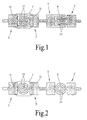
- connection facilities 3, 3 'each have a component mounting section 31 and a connecting section 32 are the connecting sections 32 of two adjacent connection devices 3, 3 'formed such that they according to the first embodiment of the present invention intermesh comb-like, an easily bridgeable Gap 6, i. H. with a predetermined slight width, is provided for a contactless structure. This ensures that the connection sections before a soldering process 32 of two adjacent connection devices 3, 3 ' do not contact.
- Components 7 to be assembled can be placed on the component assembly sections 31 two adjacent connection devices 3, 3 'are attached so that they are complete cover the connecting portions 32 protectively.
- Such a attached component 7 is shown in Fig. 1 schematically by the dashed line indicated.
- Fig. 2 shows connection devices 3, 3 'according to a second Embodiment of the present invention. Not explained Components or functions are analogous to the first Embodiment and therefore need no further explanation.
- connection sections 32 of two adjacent connection devices 3, 3 ' formed such that the connecting section the connection device 3 'circular and the correspondingly assigned connection section 32 of the connection device 3 is c-shaped, being the Connection section of the connection device 3 'contactless encloses, which in turn creates a contactless structure the gap 6 can be easily bridged.
- connection portions 32 of adjacent connection devices 3, 3 'to form an easily bridgeable Gaps 6 are matched to each other. This ensures that by applying a solder and one subsequent soldering process an electrical contact without use an additional component is created.
- the components to be assembled SMD components 7 such as glue 9 attached to the circuit board 2, that they, as in Fig. 1st can be seen on the component mounting sections 31 of the respective connection devices 3, 3 'are attached and cover the connecting portions 32 protectively.
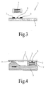
- the contact points of the components 7 with the component mounting sections 31 by placing it in a solder bath introduced to form a "wave" and thus together soldered.
- a solder short circuit is caused by applied components 7 of the connecting sections 32 underneath, as seen in Fig. 4 prevented.
- the connecting sections 32 connected by a solder bridge the were not equipped with a component.
- the present invention proceeded as follows. First of all a solder through, for example, a sieve onto the component mounting sections 31 applied with a component 7 or solder bridges to be equipped.
- the components to be assembled are in the Solder paste on the corresponding component assembly sections 31 used and for example by infrared radiation, Hotplate or hot air fused, one Solder connection between the components 7 and the corresponding ones Component placement sections 31 and between the as Adjacent connecting sections 32 serving for soldering bridges will be produced.
- connection sections are more adjacent Connection facilities conceivable.
- Soldering processes mentioned here can only be seen as an example.
Abstract
Description
Die vorliegende Erfindung betrifft eine Anschlusseinrichtung für eine Leiterplatte und Verfahren zum Bestücken derselben.The present invention relates to a connection device for a printed circuit board and method for assembling the same.
Bei der sogenannten SMD (Surface Mounted Devices)-Technik bringt man elektrische Bauelemente, z.B. Widerstände, Kondensatoren, Dioden, Transistoren und integrierte Schaltungen auf die Oberfläche von Leiterplatten auf. Hierbei werden die Bauelemente eben auf der Oberfläche der Leiterplatten mit einem Lötmittel, beispielsweise einer Lötpaste, oder nicht leitendem Kleber fixiert und dann an Anschlusseinrichtungen verlötet. Dazu sind Miniaturbauelemente mit beispielsweise komplementär ausgebildeten Anschlussflächen notwendig. Solche kleinere Bauelemente ergeben eine höhere Packungsdichte und die entsprechenden Leiterplatten können kleiner ausgebildet werden.With the so-called SMD (Surface Mounted Devices) technology bring electrical components, e.g. Resistors, capacitors, Diodes, transistors and integrated circuits the surface of printed circuit boards. Here, the components just on the surface of the PCB with a Solder, for example a solder paste, or non-conductive Adhesive fixed and then soldered to connection devices. Miniature components are complementary to this, for example trained connection surfaces necessary. Such smaller components result in a higher packing density and the corresponding Printed circuit boards can be made smaller.
Für verschiedene Anwendungen müssen Leiterplattenvarianten erstellt werden, die auch eine unterschiedliche Bestückung erfordern. Oftmals werden mehrere Leiterplatten mit verschiedenen Ausführungen verwendet.Printed circuit board variants have to be created for different applications that also require different equipment. Often, several circuit boards with different Executions used.
Alternativ wird eine unterschiedliche Bestückung mit einer Kombinations-Leiterplatte und den entsprechenden Bestückungsvarianten ausgeführt. Dabei werden die Bestückungsvarianten durch Weglassen der nicht benötigten Bauelemente bzw. durch Hinzufügen von sogenannten Null-Ohm-Widerständen als Brückenverbindung bei ansonsten offenen Verbindungen ausgeführt. Jedoch ist es nachteilhaft, dass die Null-Ohm-Widerstände zusätzliche Bearbeitungsvorgänge, zusätzliche Kleberpunkte sowie das Bauteil selbst erfordern.Alternatively, a different configuration with a Combination circuit board and the corresponding assembly variants executed. The assembly variants by omitting the components not required or by Adding so-called zero ohm resistors as a bridge connection performed on otherwise open connections. however it is disadvantageous that the zero ohm resistors are additional Processing operations, additional glue points as well require the component itself.
In Anbetracht dessen liegt der Erfindung die Aufgabe zugrunde, Anschlusseinrichtungen für eine Leiterplatte zu schaffen, mit der die Herstellung von Brückenverbindungen auf Kombinations-Leiterplatten ohne zusätzlichen Bauelemente, Bauelementekleber und ohne zusätzlichen Bearbeitungsvorgängen ausführbar ist.In view of this, the object of the invention is To create connection devices for a circuit board with of making bridge connections on combination circuit boards without additional components, component glue and can be carried out without additional processing operations.
Diese Aufgabe wird gelöst durch den Gegenstand des Anspruchs 1
und des Anspruchs 2 und die entsprechenden Verfahren gemäß Anspruch
7 und Anspruch 10.This object is achieved by the subject matter of
Die der vorliegenden Erfindung zugrundeliegende Idee besteht darin, dass jede auf der Leiterplatte angeordnete Anschlusseinrichtung mindestens einen Bauelement-Bestückungsabschnitt und wenigstens einen Verbindungsabschnitt für wenigstens eine benachbarte Anschlusseinrichtung aufweist, wobei benachbarte Verbindungsabschnitte unter Bildung eines leicht überbrückbaren Spaltes einander formangepasst sind.The idea on which the present invention is based exists in that each connection device arranged on the circuit board at least one component mounting section and at least one connecting section for at least one has adjacent connection device, wherein adjacent Connection sections to form an easily bridgeable Gaps are matched to each other.
Somit kann entweder durch ein Reflow-, Wellen- oder Schwalllöten nach Aufbringen eines Lötmittels auf einfache Weise eine Brückenverbindung ohne Verwendung eines zusätzlichen Bauelementes erzeugt werden.Thus, either by reflow, wave or wave soldering after applying a solder in a simple way Bridge connection without using an additional component be generated.
In den Unteransprüchen finden sich vorteilhafte Weiterbildungen
und Verbesserungen der in Anspruch 1 angegebenen Leiterplattenanordnung,
der in Anspruch 2 angegebenen Anschlusseinrichtung
und der in Anspruch 7 und Anspruch 10 angegebenen
Verfahren.Advantageous further developments can be found in the subclaims
and improvements to the circuit board arrangement specified in
Gemäß einer bevorzugten Weiterbildung weisen die Verbindungsabschnitte benachbarter Anschlusseinrichtungen zueinander komplementäre Formen auf. Somit wird eine gute Verbindung bei Aufbringen eines Lötmittels gewährleistet.According to a preferred development, the connecting sections Adjacent connection devices complementary to each other Forms on. Thus, a good connection is made at Guaranteed application of a solder.
Gemäß einer weiteren bevorzugten Weiterbildung greifen die Verbindungsabschnitte benachbarter Anschlusseinrichtungen jeweils kontaktlos kammförmig ineinander. Dadurch wird eine geometrisch einfache und wirksame Verbindung gewährleistet und Herstellungskosten können gering gehalten werden.According to a further preferred development, the Connection sections of adjacent connection devices in each case non-contact comb-shaped. This makes one geometric ensures simple and effective connection and Manufacturing costs can be kept low.
Gemäß einer weiteren bevorzugten Weiterbildung ist jeweils einer der benachbarten Verbindungsabschnitte kreisförmig und der entsprechende zugeordnete Verbindungsabschnitt c-förmig diesen kontaktlos umschließend ausgebildet. Dies stellt eine weitere Möglichkeit dar, im Falle des Aufbringens eines Lötmittels den Kontakt auf einfache Weise zu erzeugen, wobei ohne Lötmittel keine Verbindung aufgrund des bestehenden Spaltes existiert.According to a further preferred development, there is one of the adjacent connecting sections circular and the corresponding associated connecting section c-shaped this trained contactless enclosing. This represents another one Possibility, in the case of the application of a solder Generate contact in a simple manner, with no solder no connection exists due to the existing gap.
Gemäß einer weiteren bevorzugten Weiterbildung sind die Bauelement-Bestückungsabschnitte benachbarter Anschlusseinrichtungen gegenüberliegend und die zugeordneten Verbindungsabschnitte zwischen den entsprechenden Anschlusseinrichtungen angeordnet. Dadurch wird gewährleistet, dass beispielsweise bei einem Wellen- oder Schwalllöten die Verbindungsabschnitte dann vor einem Lötvorgang geschützt werden, wenn ein Bauelement auf den entsprechenden Bauelement-Bestückungsabschnitten angebracht ist und somit die Verbindungsabschnitte schützend abdeckt.According to a further preferred development, the component assembly sections are neighboring connection facilities opposite and the associated connecting sections between the corresponding connection devices arranged. This ensures that, for example in the case of wave or wave soldering, the connecting sections then be protected from a soldering process when a component on the corresponding component assembly sections is attached and thus protecting the connecting sections covers.
Gemäß einer weiteren bevorzugten Weiterbildung wird zum Aufbringen der Bauelemente auf der Leiterplatte und zum Herstellen der Lötbrücken an den gewünschten Stellen beispielsweise das sog. Reflow-Verfahren, das Tauch-, Wellen- oder Schwalllötverfahren verwendet. According to a further preferred development, application is carried out the components on the circuit board and for manufacturing the solder bridges at the desired locations, for example the so-called reflow process, the dip, wave or wave soldering process used.
Gemäß einer weiteren bevorzugten Weiterbildung wird beim sog. Reflow-Verfahren für das Aufbringen des Lötmittels sowohl auf den Bauelement-Bestückungsabschnitten als auch auf den Verbindungsabschnitten mindestens eine Siebeinrichtung verwendet. Dabei handelt es sich um eine Siebeinrichtung, welche die Aussparungen für ein Aufbringen eines Lötmittels auf den gewünschten Stellen aufweist.According to a further preferred development, the so-called Reflow process for applying the solder to both the component mounting sections as well as on the connecting sections used at least one screening device. It is a sieve device, which the recesses for applying a solder to the desired one Places.
Ausführungsbeispiele der Erfindung sind in den Zeichnungen dargestellt und in der nachfolgenden Beschreibung näher erläutert. Es zeigen:
- Fig. 1
- eine Draufsicht auf eine Anschlusseinrichtung gemäß einem ersten Ausführungsbeispiel der vorliegenden Erfindung;
- Fig. 2
- eine Draufsicht auf eine Anschlusseinrichtung gemäß einem zweiten Ausführungsbeispiel der vorliegenden Erfindung;
- Fig. 3
- eine Seitenansicht einer Leiterplattenanordnung mit einem aufzubringenden Bauelement; und
- Fig. 4
- eine schematische Ansicht des Prinzips eines Wellen- oder Schwalllötvorgangs.
- Fig. 1
- a plan view of a connection device according to a first embodiment of the present invention;
- Fig. 2
- a plan view of a connection device according to a second embodiment of the present invention;
- Fig. 3
- a side view of a circuit board assembly with a component to be applied; and
- Fig. 4
- a schematic view of the principle of a wave or wave soldering process.
In den Figuren bezeichnen gleiche Bezugszeichen gleiche oder funktionsgleiche Komponenten.In the figures, the same reference symbols designate the same or functionally identical components.
Fig. 1 zeigt eine Draufsicht auf zwei Paare von komplementären,
benachbarten Anschlusseinrichtungen gemäß einem ersten
Ausführungsbeispiel der vorliegenden Erfindung. Die Anschlusseinrichtungen
3, 3' besitzen jeweils einen Bauelement-Bestückungsabschnitt
31 und einen Verbindungsabschnitt 32. Dabei
sind die Verbindungsabschnitte 32 zweier benachbarter Anschlusseinrichtungen
3, 3' derart ausgebildet, dass sie gemäß
dem ersten Ausführungsbeispiel der vorliegenden Erfindung
kammförmig ineinander greifen, wobei ein leicht überbrückbarer
Spalt 6, d. h. mit einer vorbestimmten geringfügigen Breite,
für eine kontaktlose Struktur vorgesehen ist. Somit wird gewährleistet,
dass sich vor einem Lötverfahren die Verbindungsabschnitte
32 zweier benachbarter Anschlusseinrichtungen 3, 3'
nicht kontaktieren.1 shows a top view of two pairs of complementary,
adjacent connection devices according to a first
Embodiment of the present invention. The
Zu bestückende Bauelemente 7 können auf den Bauelement-Bestückungsabschnitten
31 zweier benachbarter Anschlusseinrichtungen
3, 3' derart angebracht werden, dass sie vollständig
die Verbindungsabschnitte 32 schützend abdecken. Ein derart
angebrachtes Bauelement 7 ist in Fig. 1 schematisch durch
die gestrichelte Linie angedeutet.
Fig. 2 zeigt Anschlusseinrichtungen 3, 3' gemäß einem zweiten
Ausführungsbeispiel der vorliegenden Erfindung. Nicht erläuterte
Komponenten oder Funktionsweisen sind analog zum ersten
Ausführungsbeispiel und bedürfen daher keiner weiteren Erläuterung.Fig. 2 shows
Gemäß dem zweiten Ausführungsbeispiel der vorliegenden Erfindung
sind die Verbindungsabschnitte 32 zweier benachbarter Anschlusseinrichtungen
3, 3' derart ausgebildet, das der Verbindungsabschnitt
der Anschlusseinrichtung 3' kreisförmig und der
entsprechend zugeordnete Verbindungsabschnitt 32 der Anschlusseinrichtung
3 c-förmig ausgebildet ist, wobei er den
Verbindungsabschnitt der Anschlusseinrichtung 3' kontaktlos
umschließt, wodurch wiederum eine kontaktlose Struktur durch
den leicht zuüberbrückenden Spalt 6 ausbildbar ist.According to the second embodiment of the present invention
are the connecting
In den Fig. 1 und 2 sind lediglich zwei Varianten dargestellt,
jedoch sind weitere Ausführungsbeispiele denkbar. Entscheidend
ist, dass die Verbindungsabschnitte 32 benachbarter Anschlusseinrichtungen
3, 3' unter Bildung eines leicht überbrückbaren
Spaltes 6 einander formangepasst sind. Dadurch wird gewährleistet,
dass durch Aufbringen eines Lötmittels und eines
nachfolgenden Lötverfahrens ein elektrischer Kontakt ohne Verwendung
eines züsätzlichen Bauelements geschaffen wird.1 and 2 only two variants are shown,
however, further exemplary embodiments are conceivable. critical
is that the connecting
Anhand der Fig. 3 und 4 sollen im folgenden. Verfahren zum Bestücken einer erfindungsgemäßen Leiterplattenanordnung beschrieben werden.3 and 4 are in the following. Assembly process described a circuit board assembly according to the invention become.
Bei einem Wellen- oder Schwalllötprozess werden die zu bestückenden
SMD-Bauelemente 7 beispielsweise mittels Kleber 9 derart
auf der Leiterplatte 2 befestigt, dass sie, wie in Fig. 1
ersichtlich, auf den Bauelement-Bestückungsabschnitten 31 der
jeweiligen Anschlusseinrichtungen 3, 3' angebracht sind und
die Verbindungsabschnitte 32 schützend abdecken. Danach werden
die Kontaktstellen der Bauelemente 7 mit den Bauelement-Bestückungsabschnitten
31 durch ein Einbringen in ein Lötbad
unter Bildung einer "Welle" eingebracht und somit miteinander
verlötet. Dabei wird durch aufgebrachte Bauelemente 7 ein Lötkurzschluss
der darunter liegenden Verbindungsabschnitte 32,
wie in Fig. 4 ersichtlich, verhindert. Jedoch werden die Verbindungsabschnitte
32 durch eine Lötbrücke verbunden, die
nicht durch ein Bauelement bestückt wurden.In the case of a wave or wave soldering process, the components to be assembled
Somit wird eine Lötbrücke an den gewünschten Verbindungsabschnitten einzig durch einen entsprechenden Lötvorgang geschaffen, und es sind keine zusätzlichen Bauelemente, Bauelementekleber oder Herstellungsvorgänge notwendig.This creates a solder bridge at the desired connection sections created only by an appropriate soldering process, and there are no additional components, component glue or manufacturing processes necessary.
Beim Reflow-Löten wird gemäß einem Ausführungsbeispiel der
vorliegenden Erfindung wie folgt vorgegangen. Zunächst wird
ein Lötmittel durch beispielsweise ein Sieb auf die Bauelement-Bestückungsabschnitte
31 aufgebracht, die mit einem Bauelement
7 oder Lötbrücken bestückt werden sollen. In reflow soldering, the
present invention proceeded as follows. First of all
a solder through, for example, a sieve onto the
Anschließend werden die zu bestückenden Bauelemente in die
Lötpaste auf den entsprechenden Bauelement-Bestückungsabschnitten
31 eingesetzt und beispielsweise durch Infrarot-Strahlung,
Heizplatte oder Heißluft verschmolzen , wobei eine
Lötverbindung zwischen den Bauelementen 7 und den entsprechenden
Bauelement-Bestückungsabschnitten 31 und zwischen den als
Lötbrücken dienenden benachbarten Verbindungsabschnitten 32
hergestellt wird.Then the components to be assembled are in the
Solder paste on the corresponding
Somit werden ebenfalls zur Herstellung von Lötbrücken keine zusätzlichen Bauelemente benötigt, sondern diese werden alleine durch den Lötvorgang geschaffen.Thus, none are used for the production of solder bridges additional components are required, but these are alone created by the soldering process.
Obwohl die vorliegende Erfindung anhand bevorzugter Ausführungsbeispiele vorstehend beschrieben wurde, ist sie darauf nicht beschränkt, sondern auf vielfältige Weise modifizierbar.Although the present invention is based on preferred exemplary embodiments as described above, she is on it not limited, but can be modified in a variety of ways.
So sind weitere Formgestaltungen der Verbindungsabschnitte benachbarter Anschlusseinrichtungen denkbar. Ferner sind die hier erwähnten Lötprozesse lediglich als Beispiel anzusehen. Ebenso können mehr als zwei Anschlusseinrichtungen für eine kontaktlose Struktur zueinander formangepasst ausgebildet sein. Further shapes of the connecting sections are more adjacent Connection facilities conceivable. Furthermore, the Soldering processes mentioned here can only be seen as an example. Likewise, more than two connection devices for one Contactless structure designed to match each other his.
- 11
- LeiterplattenanordnungPrinted circuit board assembly
- 22
- Leiterplattecircuit board
- 3, 3'3, 3 '
- Anschlußeinrichtungconnecting device
- 66
- Spaltgap
- 77
- Bauelementmodule
- 99
- Klebstoffadhesive
- 1010
- Lötbadsolder bath
- 3131
- Bauelement-BestückungsabschnittComponent placement section
- 3232
- Verbindungsabschnittconnecting portion
Claims (11)
dadurch gekennzeichnet, dass
jede Anschlusseinrichtung (3, 3') wenigstens einen Bauelement-Bestückungsabschnitt (31) und wenigstens einen Verbindungsabschnitt (32) für wenigstens eine benachbarte Anschlusseinrichtung (3, 3') aufweist, wobei benachbarte Verbindungsabschnitte (32) unter Bildung eines leicht überbrückbaren Spaltes (6) einander formangepasst sind.Printed circuit board arrangement (1) with a printed circuit board (2) and a plurality of connection devices (3, 3 ') arranged on the printed circuit board (2),
characterized in that
each connection device (3, 3 ') has at least one component assembly section (31) and at least one connection section (32) for at least one adjacent connection device (3, 3'), adjacent connection sections (32) forming an easily bridgeable gap (6 ) are matched to each other.
wenigstens einen Bauelement-Bestückungsabschnitt (31) und wenigstens einen Verbindungsabschnitt (32) für wenigstens eine benachbarte Anschlusseinrichtung (3, 3'), wobei benachbarte Verbindungsabschnitte (32) unter Bildung eines leicht überbrückbaren Spaltes (6) einander formangepasst sind.Connection device (3, 3 ') for a printed circuit board (2), characterized by
at least one component assembly section (31) and at least one connection section (32) for at least one adjacent connection device (3, 3 '), adjacent connection sections (32) being matched to one another to form an easily bridgeable gap (6).
Applications Claiming Priority (2)
| Application Number | Priority Date | Filing Date | Title |
|---|---|---|---|
| DE10108780 | 2001-02-23 | ||
| DE10108780A DE10108780A1 (en) | 2001-02-23 | 2001-02-23 | Connection device for a printed circuit board and method for equipping the same |
Publications (1)
| Publication Number | Publication Date |
|---|---|
| EP1235470A1 true EP1235470A1 (en) | 2002-08-28 |
Family
ID=7675262
Family Applications (1)
| Application Number | Title | Priority Date | Filing Date |
|---|---|---|---|
| EP01107909A Withdrawn EP1235470A1 (en) | 2001-02-23 | 2001-03-28 | Contact pad arrangement for a printed circuit board and process for mounting components thereon |
Country Status (2)
| Country | Link |
|---|---|
| EP (1) | EP1235470A1 (en) |
| DE (1) | DE10108780A1 (en) |
Families Citing this family (2)
| Publication number | Priority date | Publication date | Assignee | Title |
|---|---|---|---|---|
| DE10344631B4 (en) * | 2003-09-25 | 2013-12-24 | Robert Bosch Gmbh | Electronic circuitry |
| DE202010008479U1 (en) * | 2010-09-08 | 2011-12-09 | Zumtobel Lighting Gmbh | Printed circuit board for fitting with luminous bodies |
Citations (6)
| Publication number | Priority date | Publication date | Assignee | Title |
|---|---|---|---|---|
| DE2111502A1 (en) * | 1971-03-10 | 1972-09-21 | Siemens Ag | Method for equipping building panels with preferably electrical components |
| US4379318A (en) * | 1979-09-21 | 1983-04-05 | Nissan Motor Company, Limited | Overcurrent safety construction for a printed circuit board |
| US4982892A (en) * | 1989-11-09 | 1991-01-08 | International Business Machines Corporation | Solder interconnects for selective line coupling |
| US5303122A (en) * | 1991-10-31 | 1994-04-12 | Ford Motor Company | Printed circuit board having a commonized mounting pad which different sized surface mounted devices can be mounted |
| JPH0786729A (en) * | 1993-09-09 | 1995-03-31 | Ibiden Co Ltd | Connection structure of jumper land in printed-wiring board and connection of jumper land |
| JPH08279661A (en) * | 1995-04-10 | 1996-10-22 | Matsushita Electric Ind Co Ltd | Printed board |
-
2001
- 2001-02-23 DE DE10108780A patent/DE10108780A1/en not_active Withdrawn
- 2001-03-28 EP EP01107909A patent/EP1235470A1/en not_active Withdrawn
Patent Citations (6)
| Publication number | Priority date | Publication date | Assignee | Title |
|---|---|---|---|---|
| DE2111502A1 (en) * | 1971-03-10 | 1972-09-21 | Siemens Ag | Method for equipping building panels with preferably electrical components |
| US4379318A (en) * | 1979-09-21 | 1983-04-05 | Nissan Motor Company, Limited | Overcurrent safety construction for a printed circuit board |
| US4982892A (en) * | 1989-11-09 | 1991-01-08 | International Business Machines Corporation | Solder interconnects for selective line coupling |
| US5303122A (en) * | 1991-10-31 | 1994-04-12 | Ford Motor Company | Printed circuit board having a commonized mounting pad which different sized surface mounted devices can be mounted |
| JPH0786729A (en) * | 1993-09-09 | 1995-03-31 | Ibiden Co Ltd | Connection structure of jumper land in printed-wiring board and connection of jumper land |
| JPH08279661A (en) * | 1995-04-10 | 1996-10-22 | Matsushita Electric Ind Co Ltd | Printed board |
Non-Patent Citations (3)
| Title |
|---|
| PARLA A ET AL: "SOLDER INTERCONNECTIONS FOR SMT SELECTIVE LINE COUPLING", IEEE TRANSACTIONS ON COMPONENTS,HYBRIDS,AND MANUFACTURING TECHNOLOGY, IEEE INC. NEW YORK, US, vol. 14, no. 4, 1 December 1991 (1991-12-01), pages 738 - 743, XP000274247, ISSN: 0148-6411 * |
| PATENT ABSTRACTS OF JAPAN vol. 1995, no. 06 31 July 1995 (1995-07-31) * |
| PATENT ABSTRACTS OF JAPAN vol. 1997, no. 02 28 February 1997 (1997-02-28) * |
Also Published As
| Publication number | Publication date |
|---|---|
| DE10108780A1 (en) | 2002-09-05 |
Similar Documents
| Publication | Publication Date | Title |
|---|---|---|
| EP0762817A1 (en) | Shielding for flat assemblies | |
| DE19651122C2 (en) | Semiconductor component with a semiconductor chip and a circuit board | |
| DE3535923C2 (en) | ||
| DE3607049C2 (en) | ||
| DE2852753B2 (en) | Method for fastening components with flat connection contacts on a printed circuit board | |
| EP1393605B1 (en) | Circuit board with at least one electronic component | |
| DE3209914A1 (en) | HEARING DEVICE WITH AN AMPLIFIER CIRCUIT | |
| EP0464232B1 (en) | Solder connector and process for making an electrical circuit with this solder connector | |
| DE3501710C2 (en) | ||
| DE60128537T2 (en) | ASSEMBLY TO CONNECT AT LEAST TWO PRINTED CIRCUITS | |
| EP1665914A1 (en) | Printed circuit board comprising a holding device for retaining wired electronic components, method for the production of such a printed circuit board, and use thereof in a soldering furnace | |
| EP0613331B1 (en) | Method of attaching a hybrid circuit on a pcb | |
| WO2002093992A1 (en) | Printed circuit board comprising a contact sleeve that is mounted thereon | |
| DE3138987C2 (en) | Device for preventing damage to components or conductor tracks on a circuit board | |
| EP1606982B1 (en) | Method for electrically and mechanically connecting two printed boards | |
| EP1235470A1 (en) | Contact pad arrangement for a printed circuit board and process for mounting components thereon | |
| DE112015003374T5 (en) | circuitry | |
| DE102012112546A1 (en) | Method for manufacturing mixed printed circuit board of measuring device, involves printing stencil with solder paste, and fitting surface mount device components with side of board, where components are soldered during soldering process | |
| DE19512272C2 (en) | Method for producing a multilayer printed circuit board for a chassis of a consumer electronic device and printed circuit board produced according to this method | |
| DE3523646A1 (en) | MULTILAYER CIRCUIT BOARD WITH PLATED THROUGH HOLES | |
| EP0968629B1 (en) | Flat assembly and method for post-assembling additional components on a printed circuit board | |
| EP0144413A1 (en) | Printed board for the surface soldering of integrated miniature circuits and manufacturing method of such printed boards | |
| EP0304902B1 (en) | Arrangement for modifying and/or repairing a flat module when inserting surface-mounted components | |
| DE4208594A1 (en) | Prefabricated electrical component fixing to PCB - serially mfg. unitary circuits for selective imposition on regions of circuit board requiring rectification or extension | |
| EP1111974B1 (en) | Process for manufacturing a solder connection |
Legal Events
| Date | Code | Title | Description |
|---|---|---|---|
| PUAI | Public reference made under article 153(3) epc to a published international application that has entered the european phase |
Free format text: ORIGINAL CODE: 0009012 |
|
| AK | Designated contracting states |
Kind code of ref document: A1 Designated state(s): AT BE CH CY DE DK ES FI FR GB GR IE IT LI LU MC NL PT SE TR |
|
| AX | Request for extension of the european patent |
Free format text: AL;LT;LV;MK;RO;SI |
|
| 17P | Request for examination filed |
Effective date: 20021202 |
|
| AKX | Designation fees paid |
Designated state(s): DE FR |
|
| STAA | Information on the status of an ep patent application or granted ep patent |
Free format text: STATUS: THE APPLICATION HAS BEEN WITHDRAWN |
|
| 18W | Application withdrawn |
Effective date: 20060104 |