EP1245642A1 - Siloxane-based resin and method for forming an insulating film between interconnecting layers in wafers - Google Patents
Siloxane-based resin and method for forming an insulating film between interconnecting layers in wafers Download PDFInfo
- Publication number
- EP1245642A1 EP1245642A1 EP02251958A EP02251958A EP1245642A1 EP 1245642 A1 EP1245642 A1 EP 1245642A1 EP 02251958 A EP02251958 A EP 02251958A EP 02251958 A EP02251958 A EP 02251958A EP 1245642 A1 EP1245642 A1 EP 1245642A1
- Authority
- EP
- European Patent Office
- Prior art keywords
- siloxane
- alkoxy
- halo
- alkyl
- independently
- Prior art date
- Legal status (The legal status is an assumption and is not a legal conclusion. Google has not performed a legal analysis and makes no representation as to the accuracy of the status listed.)
- Granted
Links
Classifications
-
- C—CHEMISTRY; METALLURGY
- C08—ORGANIC MACROMOLECULAR COMPOUNDS; THEIR PREPARATION OR CHEMICAL WORKING-UP; COMPOSITIONS BASED THEREON
- C08G—MACROMOLECULAR COMPOUNDS OBTAINED OTHERWISE THAN BY REACTIONS ONLY INVOLVING UNSATURATED CARBON-TO-CARBON BONDS
- C08G77/00—Macromolecular compounds obtained by reactions forming a linkage containing silicon with or without sulfur, nitrogen, oxygen or carbon in the main chain of the macromolecule
- C08G77/04—Polysiloxanes
- C08G77/06—Preparatory processes
-
- C—CHEMISTRY; METALLURGY
- C08—ORGANIC MACROMOLECULAR COMPOUNDS; THEIR PREPARATION OR CHEMICAL WORKING-UP; COMPOSITIONS BASED THEREON
- C08G—MACROMOLECULAR COMPOUNDS OBTAINED OTHERWISE THAN BY REACTIONS ONLY INVOLVING UNSATURATED CARBON-TO-CARBON BONDS
- C08G77/00—Macromolecular compounds obtained by reactions forming a linkage containing silicon with or without sulfur, nitrogen, oxygen or carbon in the main chain of the macromolecule
- C08G77/04—Polysiloxanes
-
- C—CHEMISTRY; METALLURGY
- C08—ORGANIC MACROMOLECULAR COMPOUNDS; THEIR PREPARATION OR CHEMICAL WORKING-UP; COMPOSITIONS BASED THEREON
- C08G—MACROMOLECULAR COMPOUNDS OBTAINED OTHERWISE THAN BY REACTIONS ONLY INVOLVING UNSATURATED CARBON-TO-CARBON BONDS
- C08G77/00—Macromolecular compounds obtained by reactions forming a linkage containing silicon with or without sulfur, nitrogen, oxygen or carbon in the main chain of the macromolecule
- C08G77/48—Macromolecular compounds obtained by reactions forming a linkage containing silicon with or without sulfur, nitrogen, oxygen or carbon in the main chain of the macromolecule in which at least two but not all the silicon atoms are connected by linkages other than oxygen atoms
- C08G77/50—Macromolecular compounds obtained by reactions forming a linkage containing silicon with or without sulfur, nitrogen, oxygen or carbon in the main chain of the macromolecule in which at least two but not all the silicon atoms are connected by linkages other than oxygen atoms by carbon linkages
-
- C—CHEMISTRY; METALLURGY
- C09—DYES; PAINTS; POLISHES; NATURAL RESINS; ADHESIVES; COMPOSITIONS NOT OTHERWISE PROVIDED FOR; APPLICATIONS OF MATERIALS NOT OTHERWISE PROVIDED FOR
- C09D—COATING COMPOSITIONS, e.g. PAINTS, VARNISHES OR LACQUERS; FILLING PASTES; CHEMICAL PAINT OR INK REMOVERS; INKS; CORRECTING FLUIDS; WOODSTAINS; PASTES OR SOLIDS FOR COLOURING OR PRINTING; USE OF MATERIALS THEREFOR
- C09D183/00—Coating compositions based on macromolecular compounds obtained by reactions forming in the main chain of the macromolecule a linkage containing silicon, with or without sulfur, nitrogen, oxygen, or carbon only; Coating compositions based on derivatives of such polymers
- C09D183/04—Polysiloxanes
-
- H—ELECTRICITY
- H01—ELECTRIC ELEMENTS
- H01B—CABLES; CONDUCTORS; INSULATORS; SELECTION OF MATERIALS FOR THEIR CONDUCTIVE, INSULATING OR DIELECTRIC PROPERTIES
- H01B3/00—Insulators or insulating bodies characterised by the insulating materials; Selection of materials for their insulating or dielectric properties
- H01B3/18—Insulators or insulating bodies characterised by the insulating materials; Selection of materials for their insulating or dielectric properties mainly consisting of organic substances
- H01B3/30—Insulators or insulating bodies characterised by the insulating materials; Selection of materials for their insulating or dielectric properties mainly consisting of organic substances plastics; resins; waxes
- H01B3/46—Insulators or insulating bodies characterised by the insulating materials; Selection of materials for their insulating or dielectric properties mainly consisting of organic substances plastics; resins; waxes silicones
-
- H—ELECTRICITY
- H01—ELECTRIC ELEMENTS
- H01L—SEMICONDUCTOR DEVICES NOT COVERED BY CLASS H10
- H01L21/00—Processes or apparatus adapted for the manufacture or treatment of semiconductor or solid state devices or of parts thereof
- H01L21/02—Manufacture or treatment of semiconductor devices or of parts thereof
- H01L21/02104—Forming layers
- H01L21/02107—Forming insulating materials on a substrate
- H01L21/02109—Forming insulating materials on a substrate characterised by the type of layer, e.g. type of material, porous/non-porous, pre-cursors, mixtures or laminates
- H01L21/02112—Forming insulating materials on a substrate characterised by the type of layer, e.g. type of material, porous/non-porous, pre-cursors, mixtures or laminates characterised by the material of the layer
- H01L21/02123—Forming insulating materials on a substrate characterised by the type of layer, e.g. type of material, porous/non-porous, pre-cursors, mixtures or laminates characterised by the material of the layer the material containing silicon
- H01L21/02126—Forming insulating materials on a substrate characterised by the type of layer, e.g. type of material, porous/non-porous, pre-cursors, mixtures or laminates characterised by the material of the layer the material containing silicon the material containing Si, O, and at least one of H, N, C, F, or other non-metal elements, e.g. SiOC, SiOC:H or SiONC
-
- H—ELECTRICITY
- H01—ELECTRIC ELEMENTS
- H01L—SEMICONDUCTOR DEVICES NOT COVERED BY CLASS H10
- H01L21/00—Processes or apparatus adapted for the manufacture or treatment of semiconductor or solid state devices or of parts thereof
- H01L21/02—Manufacture or treatment of semiconductor devices or of parts thereof
- H01L21/02104—Forming layers
- H01L21/02107—Forming insulating materials on a substrate
- H01L21/02109—Forming insulating materials on a substrate characterised by the type of layer, e.g. type of material, porous/non-porous, pre-cursors, mixtures or laminates
- H01L21/02203—Forming insulating materials on a substrate characterised by the type of layer, e.g. type of material, porous/non-porous, pre-cursors, mixtures or laminates the layer being porous
-
- H—ELECTRICITY
- H01—ELECTRIC ELEMENTS
- H01L—SEMICONDUCTOR DEVICES NOT COVERED BY CLASS H10
- H01L21/00—Processes or apparatus adapted for the manufacture or treatment of semiconductor or solid state devices or of parts thereof
- H01L21/02—Manufacture or treatment of semiconductor devices or of parts thereof
- H01L21/02104—Forming layers
- H01L21/02107—Forming insulating materials on a substrate
- H01L21/02109—Forming insulating materials on a substrate characterised by the type of layer, e.g. type of material, porous/non-porous, pre-cursors, mixtures or laminates
- H01L21/02205—Forming insulating materials on a substrate characterised by the type of layer, e.g. type of material, porous/non-porous, pre-cursors, mixtures or laminates the layer being characterised by the precursor material for deposition
- H01L21/02208—Forming insulating materials on a substrate characterised by the type of layer, e.g. type of material, porous/non-porous, pre-cursors, mixtures or laminates the layer being characterised by the precursor material for deposition the precursor containing a compound comprising Si
- H01L21/02214—Forming insulating materials on a substrate characterised by the type of layer, e.g. type of material, porous/non-porous, pre-cursors, mixtures or laminates the layer being characterised by the precursor material for deposition the precursor containing a compound comprising Si the compound comprising silicon and oxygen
- H01L21/02216—Forming insulating materials on a substrate characterised by the type of layer, e.g. type of material, porous/non-porous, pre-cursors, mixtures or laminates the layer being characterised by the precursor material for deposition the precursor containing a compound comprising Si the compound comprising silicon and oxygen the compound being a molecule comprising at least one silicon-oxygen bond and the compound having hydrogen or an organic group attached to the silicon or oxygen, e.g. a siloxane
-
- H—ELECTRICITY
- H01—ELECTRIC ELEMENTS
- H01L—SEMICONDUCTOR DEVICES NOT COVERED BY CLASS H10
- H01L21/00—Processes or apparatus adapted for the manufacture or treatment of semiconductor or solid state devices or of parts thereof
- H01L21/02—Manufacture or treatment of semiconductor devices or of parts thereof
- H01L21/02104—Forming layers
- H01L21/02107—Forming insulating materials on a substrate
- H01L21/02225—Forming insulating materials on a substrate characterised by the process for the formation of the insulating layer
- H01L21/0226—Forming insulating materials on a substrate characterised by the process for the formation of the insulating layer formation by a deposition process
- H01L21/02282—Forming insulating materials on a substrate characterised by the process for the formation of the insulating layer formation by a deposition process liquid deposition, e.g. spin-coating, sol-gel techniques, spray coating
Definitions
- the present invention relates to a siloxane-based resin and a method for forming insulating film between interconnect layers in semiconductor devices by using the same. More specifically, the present invention relates to a siloxane-based resin prepared by hydrolyzing and polycondensing cyclic and/or cage-shape siloxane compounds, optionally with at least one silane compound, in an organic solvent in the presence of a catalyst and water. The present invention also relates to a method for forming insulating film between interconnect layers in semiconductor devices, wherein the siloxane-based resin described above is used as low dielectric insulating materials.
- polysilsesquioxanes having dielectric constant of approximately 2.5 ⁇ 3.1 has replaced SiO 2 having dielectric constant of 4.0 in chemical vapor deposition(CVD).
- Such polysilsesquioxanes can be also applied to a spin coating method due to its excellent planation property.
- US Patent No. 3,615,272 discloses a method for preparing completely condensed soluble hydrogensilsesquioxane resins, which comprises the steps of condensing trichlorosilanes in a sulfuric acid medium, and then washing the resulting resins with water or aqueous sulfuric acid.
- US Patent No. 5,010,159 discloses a method for synthesizing soluble condensed hydridosilicon resins, which comprises the steps of hydrolyzing hydridosilanes in an arylsulfuric acid hydrate-containing hydrolysis medium, and then contacting the resulting resins with a neutralizing agent.
- 6,232,424 describes a highly soluble silicone resin composition having excellent solution stability, which was prepared by hydrolyzing and polycondensing tetraalkoxysilane, organosilane and organotrialkoxysilane monomers in the presence of water and a catalyst.
- US Patent No. 6,000,339 teaches that a silica-based compound, which may be useful for improving the resistance and physical properties as well as thickness of a coating film, can be obtained from a reaction of a monomer selected from the group consisting of alkoxysilane, fluorine-containing alkoxysilane and alkylalkoxysilane and a titanium- or zirconium-alkoxide compound in the presence of water and a catalyst.
- the prior polysilsesquioxane resins have not accomplished very low dielectric constant that is currently required for insulating film between interconnect layers in semiconductor devices. Additionally, they have been required to improve in mechanical properties, thermal stability, crack-resistance, and so on.
- a feature of the present invention is a method for forming low dielectric insulating film between interconnect layers in semiconductor devices by using a siloxane-based resin having very low dielectric constant, wherein the resin is obtained from the copolymerization of cyclic and/or cage-shape siloxane compounds optionally with one or more silane compounds.
- An aspect of the present invention relates to siloxane-based resins that are prepared by hydrolyzing and polycondensing a cyclic siloxane compound of formula (1) and a cage-shape siloxane compound of any of formulas (2a)-(2c) in an organic solvent in the presence of a catalyst and water: wherein, R is H, C 1-3 alkyl, C 3-10 cycloalkyl, or C 6-15 aryl; each of X 1 , X 2 , and X 3 is, independently, C 1-3 alkyl, C 1-10 alkoxy, or halo, provided that at least one is alkoxy or halo; p is an integer from 3 to 8; and m is an integer from 1 to 10; in the above formulas (2a)-(2c), each of X 1 , X 2 , and X 3 is, independently, C 1-3 alkyl, C 1-10 alkoxy, or halo, provided that at least one is alkoxy or halo
- siloxane-based resins that are prepared by hydrolyzing and polycondensing a cyclic siloxane compound of formula (1) and a cage-shape siloxane compound of any of formulas (2a)-(2c), together with a silane compound of formula (3) and/or a silane compound of formula (4), in an organic solvent in the presence of a catalyst and water: wherein, R is H, C 1-3 alkyl, C 3-10 cycloalkyl, or C 6-15 aryl; each of X 1 , X 2 , and X 3 is, independently, C 1-3 alkyl, C 1-10 alkoxy, or halo, provided that at least one is alkoxy or halo; p is an integer from 3 to 8; and m is an integer from 1 to 10; in the above formulas 2(a)-2(c), each of X 1 , X 2 , and X 3 is, independently, C 1-3 alkyl, C 1-10
- Still another aspect of the present invention relates to siloxane-based resins that are prepared by hydrolyzing and polycondensing a cyclic siloxane compound of formula (1), together with a silane compound of formula (3) and/or a silane compound of formula (4), in an organic solvent in the presence of a catalyst and water: wherein, R is H, C 1-3 alkyl, C 3-10 cycloalkyl, or C 6-15 aryl; each of X 1 , X 2 , and X 3 is, independently, C 1-3 alkyl, C 1-10 alkoxy, or halo, provided that at least one is alkoxy or halo; p is an integer from 3 to 8; and m is an integer from 1 to 10; SiX 1 X 2 X 3 X 4 wherein, each of X 1 , X 2 , X 3 , and X 4 is, independently, C 1-10 alkoxy, or halo; RSiX 1 X 2 X 3 wherein,
- Still another aspect of the present invention relates to siloxane-based resins that are prepared by hydrolyzing and polycondensing a cage-shape siloxane compound of any of formulas (2a)-(2c), together with a silane compound of formula (3) and/or a silane compound of formula (4), in an organic solvent in the presence of a catalyst and water: in the above formulas (2a)-(2c), each of X 1 , X 2 , and X 3 is, independently, C 1-3 alkyl, C 1-10 alkoxy, or halo, provided that at least one is alkoxy or halo; and n is an integer from 1 to 12; SiX 1 X 2 X 3 X 4 wherein, each of X 1 , X 2 , X 3 , and X 4 is, independently, C 1-10 alkoxy, or halo; RSiX 1 X 2 X 3 wherein, R is H, C 1-3 alkyl, C 3-10 cycloal
- Still another aspect of the present invention relates to a method for forming insulating film between interconnect layers in semiconductor devices, the method comprising the steps of: providing a resinous solution by dissolving the siloxane-based resin described above in an organic solvent; coating a silicon wafer with the resinous solution; and heat-curing the resulting coating film.
- a siloxane-based resin of the present invention is prepared by hydrolyzing and polycondensing cyclic and/or cage-shape siloxane monomers, optionally with at least one silane monomer, in an organic solvent in the presence of a catalyst and water.
- the cyclic siloxane monomers used in the present invention can be represented by the following formula (1): wherein, R is H, C 1-3 alkyl, C 3 - 10 cycloalkyl, or C 6 - 15 aryl; each of X 1 , X 2 , and X 3 is, independently, C 1 - 3 alkyl, C 1 - 10 alkoxy, or halo, provided that at least one is alkoxy or halo; p is an integer from 3 to 8; and m is an integer from 1 to 10.
- cyclic siloxane monomers may be obtained from a hydrosililation reaction using a metal catalyst.
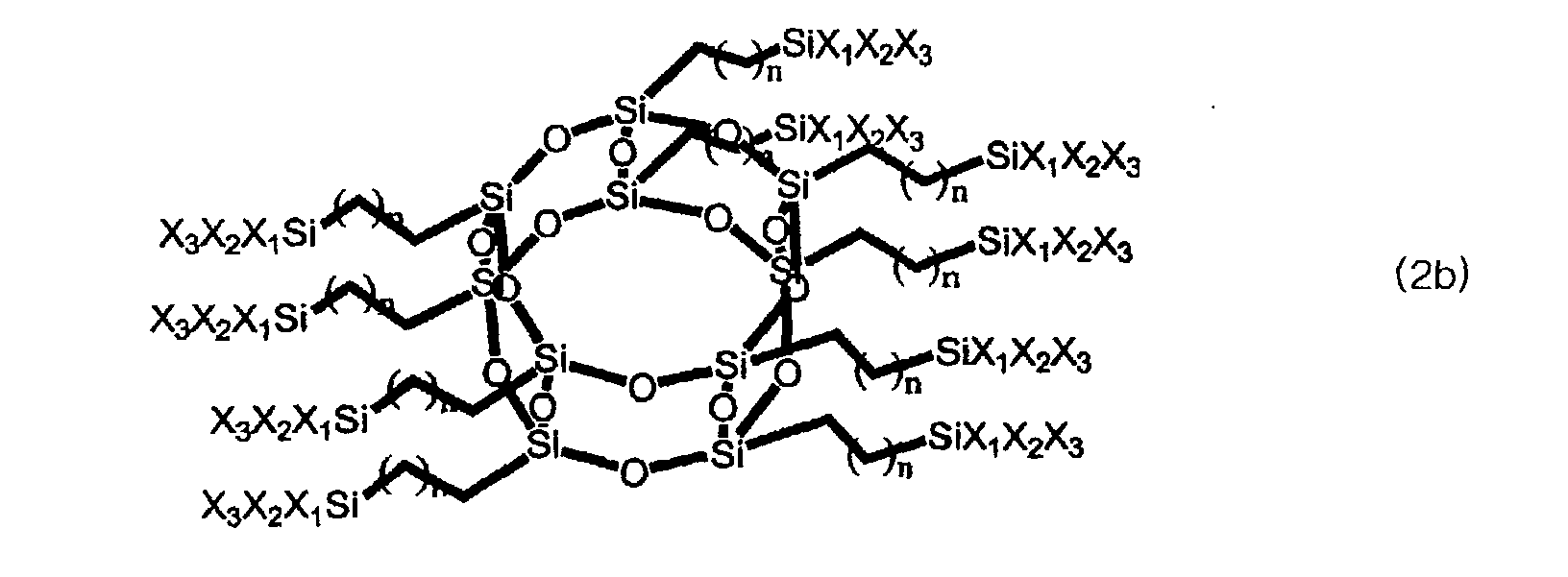
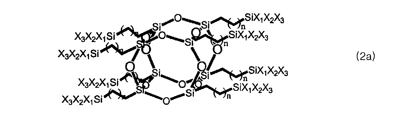
- the cage-shape siloxane monomers used in the present invention can be represented by one of the following formulas (2a)-(2c): in the above formulas (2a)-(2c), each of X 1 , X 2 , and X 3 is, independently, C 1 - 3 alkyl, C 1 - 10 alkoxy, or halo, provided that at least one is alkoxy or halo; and n is an integer from 1 to 12.
- two silicon atoms are linked to each other through an oxygen atom to form cyclic structure, and the terminal of each branch comprises at least one hydrolysable group.
- cage-shape siloxane monomers commercially available ones whose terminal functional groups are halogens can be used, without modification or after substitution of the terminal halogens with alkyl and/or alkoxy groups. Such substitution may be accomplished by any of standard methods well known in the art. For example, the substitution of the terminal halogens with alkoxy groups can be readily accomplished through reacting the halogenated cage-shape siloxane compound with an alcohol and a triethylamine.
- silane monomers used in the present invention can be represented by the following formula (3), in which Si has four hydrolysable substituents: SiX 1 X 2 X 3 X 4 wherein, each of X 1 , X 2 , X 3 , and X 4 is, independently, C 1-10 alkoxy, or halo.
- Non-limiting examples of such silane monomer include tetra-n-butoxysilane, tetra-n-propoxysilane, tetraethoxysilane, tetramethoxysilane, tetrachlorosilane, tetrabromosilane, tetrafluorosilane, triethoxychlorosilane, and trimethoxychlorosilane.
- the other silane monomers represented by the following formula (4) can be used in the preparation of the siloxane-based resins of the present invention, in which Si has at least one hydrolysable substituent: RSiX 1 X 2 X 3 wherein, R is H, C 1-3 alkyl, C 3-10 cycloalkyl, or C 6-15 aryl; and each of X 1 , X 2 , and X 3 is, independently, C 1-3 alkyl, C 1-10 alkoxy, or halo, provided that at least one is alkoxy or halo.
- Non-limiting examples of such silane monomer include methyltriethoxysilane, methyltrimethoxysilane, methyltri-n-propoxysilane, phenyltrimethoxysilane, phenyltriethoxysilane, phenyltrichlorosilane, phenyltrifluorosilane, methyltrichlorosilane, methyltribromosilane, methyltrifluorosilane, triethoxysilane, trimethoxysilane, trichlorosilane, and trifluorosilane.
- siloxane-based resins of the present invention can be obtained as copolymeric products from the hydrolysis and polycondensation of the cyclic siloxane compound of formula (1)(hereinafter, referred to as siloxane compound (1)) and the cage-shape siloxane compound of formula (2) (hereinafter, referred to as siloxane compound (2)) in an organic solvent in the presence of a catalyst and water.
- the siloxane-based resins of the present invention can be prepared by hydrolyzing and polycondensing either or both of siloxane compounds (1) and (2), together with either or both of the silane compound of formula (3)(hereinafter, referred to as silane compound (3)) and the silane compound of formula (4) (hereinafter, referred to as silane compound (4)), in an organic solvent in the presence of a catalyst and water.
- the molar ratio of compound (1) vs. compound (2) is between 0.1:99.9 and 99.9:0.1, preferably 5:95 and 50:50.
- a quaternary copolymer can be prepared by using both silane compounds (3) and (4) in conjunction with both siloxane compounds (1) and (2). At this time, each of the four compounds is used in an amount of 1-97mol%, respectively.
- both cyclic and cage-shape siloxane compounds are not always used in combination, and thus it is also possible to use either of the cyclic and cage-shape siloxane compounds.
- silane compound (3) is preferably copolymerized therewith to provide a binary copolymer, wherein the molar ratio of compound (1) vs. compound (3) is between 99.9:0.1 and 0.1:99.9, preferably 95:5 and 50:50.
- silane compound (4) can be additionally employed in the copolymerization to provide a ternary copolymer. This ternary copolymer contains 1-98mol% of compound (1), 1-98mol% of compound (3), and 1-98mol% of compound (4).
- silane compound (4) is preferably copolymerized therewith to provide a binary copolymer, wherein the molar ratio of compound (2) vs. compound (4) is between 0.1:99.9 and 99.9:0.1, preferably 5:95 and 50:50.
- silane compound (3) can be further added to the copolymerization reaction to provide a ternary copolymer. This ternary copolymer contains 1-98mol% of compound (2), 1-98mol% of compound (3), and 1-98mol% of compound (4).
- organic solvents used in the preparation of the siloxane-based resins according to the present invention aromatic hydrocarbon solvent, aliphatic hydrocarbon solvent, ketone-based solvent, ether-based solvent, acetate-based solvent, alcohol-based solvent, silicon-based solvent, or mixtures thereof are preferred.
- Exemplary catalysts used in the present invention include, without limitation, hydrochloric acid, nitric acid, benzene sulfonic acid, oxalic acid, formic acid, potassium hydroxide, sodium hydroxide, triethylamine, sodium bicarbonate, pyridine, and mixtures thereof.
- the molar ratio of the catalyst vs. monomers to be polymerized(inclusive of siloxane and silane compounds) is preferably between 0.00001:1 and 10:1. Further, 0.1-1,000mol of water is added to 1mol of the monomers. Then, the hydrolysis and polycondensation are carried out at a temperature of 0-200°C, preferably 50-110°C, for 0.1-100hrs, preferably 3-48hrs.
- the siloxane-based resins thus prepared have Mw of 3,000 to 500,000, preferably 3,000 to 100,000.
- Si-OR content in the whole terminal groups represented by Si-OR and/or Si-R is more than 5mol%, wherein R is H, C 1-3 alkyl, C 3-10 cycloalkyl, or C 6-15 aryl.
- the siloxane-based resins of the present invention can be used as matrix precursors of insulating film between interconnect layers in semiconductor devices.
- a method for forming insulating film between interconnect layers in semiconductor devices of the present invention comprises the steps of: providing a resinous solution by dissolving the siloxane-based resin in an organic solvent; coating a silicon wafer with the resinous solution; and heating the coated wafer to cure the resin.
- the resinous solution can further comprise a porogen, which is a pore-generating material.
- a porogen which is a pore-generating material.
- the porogen useful in the present invention include cyclodextrin and derivatives thereof described in Korean Patent Appln. No. 2001-15883, as well as polycaprolactone and derivatives thereof described in U.S. Patent No. 6,114,458.
- Preferred mixing ratio of the siloxane-based resin vs. porogen is between 99:1 and 30:70(w/w), more preferably 90:10 and 50:50(w/w).
- Preferred organic solvents used in dissolution of the siloxane-based resin or a mixture of the siloxane-based resin and porogen to provide a resinous solution can be exemplified by, but are not limited to, aliphatic hydrocarbon solvents; aromatic hydrocarbon solvents such as anisole, mesitylene and xylene; ketone-based solvents such as methyl isobutyl ketone, 1-methyl-2-pyrrolidinone, cyclohexanone and acetone; ether-based solvents such as tetrahydrofuran and isopropyl ether; acetate-based solvents such as ethyl acetate, butyl acetate and propylene glycol methyl ether acetate; alcohol-based solvents such as isopropyl alcohol, butyl alcohol and octyl alcohol; amide-based solvents such as dimethylacetamide and dimethylformamide; silicon-based solvents; and mixtures thereof.
- the organic solvent Upon preparing a resinous solution, the organic solvent should be used in a sufficient amount to apply the resin component evenly on the surface of a wafer.
- the organic solvent is added to the siloxane-based resin or to the mixture of the siloxane-based resin and porogen so that final concentration of the solid matter(inclusive of the siloxane-based resin and the porogen) is 0.1-80wt%, preferably 5-40wt%.
- Non-limiting examples of the method for coating a silicon wafer with the resinous solution thus prepared include spin-coating, dip-coating, spray-coating, flow-coating, and screen-printing, while spin-coating is most preferred.
- spin coating the spin rate is controlled to be between 1,000 and 5,000rpm.
- the organic solvent is evaporated from the wafer so that a resinous film comprising the siloxane-based resin can deposit on the wafer.
- the evaporation may be carried out by simple air-drying, or by subjecting the wafer, at the beginning of following curing step, to a vacuum condition or mild heating( ⁇ 100°C).
- the resinous film is cured by heating for 1-150min at a temperature of 150-600°C, preferably 200-450°C, so as to provide a insoluble, crack-free film.
- crack-free film is meant a film without any crack observed with an optical microscope at a magnification of 1000X.
- insoluble film is meant a film that is substantially insoluble in any solvent described as being useful for dissolving the siloxane-based resins.
- the coating film thus formed was found to have dielectric constant below 3.0, preferably between 2.0 and 2.7, and so it is very useful as an insulating film between interconnect layers in semiconductor devices.
- Example 1-1 Copolymerization of cyclic and cage-shape siloxane monomers
- Cyclic and cage-shape siloxane monomers were quantified respectively according to Table 1, and then added to a flask, followed by dilution with 45ml of tetrahydrofuran. Thereafter, the flask was cooled to -78°C, and HCl and deionized water were slowly added thereto at the same temperature, and then it was slowly warmed to 70°C. The reaction was continued at 70°C for 16hrs, and transferred to a separatory funnel, followed by addition of 90ml of diethylether. After washing with 3X50ml of deionized water, volatile materials were evaporated from the remaining solution to afford a white powdery polymer.
- the powder was dissolved in a small amount of acetone, and filtered through a 0.2 ⁇ m syringe filter so as to remove impurities to provide a clear filtrate. After addition of water to the filtrate, the resulting white powder was separated from the liquid phase(mixed solution of acetone and water), and then dried at a temperature of 0-5°C under a reduced pressure of about 0.1Torr to afford a fractionated siloxane-based resin.
- Example 1-2 Copolymerization of cyclic and cage-shape siloxane monomers together with a silane monomer of formula (3)
- Cyclic and cage-shape siloxane monomers as well as tetramethoxysilane as a silane monomer of formula (3) were quantified respectively according to Table 2, and then added to a flask, followed by dilution with 50ml of tetrahydrofuran. Thereafter, the flask was cooled to -78°C, and HCl and deionized water were slowly added thereto at the same temperature, and then it was slowly warmed to 60°C. The reaction was continued at 60°C for 16hrs, and transferred to a separatory funnel, followed by addition of 150ml of diethylether.
- Example 1-3 Copolymerization of cyclic and cage-shape siloxane monomers together with silane monomers of formulas (3) and (4)
- Example 1-3 The procedure of Example 1-3 was conducted according to the same manner as in the above Example 1-2, except that methyltrimethoxysilane was additionally used as a silane monomer of formula (4).
- Resin Monomers mmol
- HCl mmol
- H 2 O mmol
- Yield g
- Cyclic siloxane Cage-shape siloxane Silane Monomer A
- Monomer C
- Tetramethoxysilane Methyltrimethoxysilane 9.598 1.200 5.144 1.197 1.490 496.428 4.76
- Example 1-4 Copolymerization of a cyclic siloxane monomer together with a silane monomer of formula (3)
- Example 1-4 The procedure of Example 1-4 was conducted according to the same manner as in the above Example 1-2, except that the cage shape siloxane monomer was omitted.
- Resin Monomers mmol
- HCl mmol
- H 2 O mmol
- Yield g
- Cyclic siloxane Silane Monomer A) Tetramethoxysilane (g) 5.999 0.667 0.747 248.828 2.39 (h) 5.999 2.571 0.823 274.213 2.46 (i) 5.999 5.999 0.960 319.915 2.53
- Example 1-5 Copolymerization of a cyclic siloxane monomer together with silane monomers of formulas (3) and (4)
- Example 1-5 The procedure of Example 1-5 was conducted according to the same manner as in the above Example 1-4, except that methyltrimethoxysilane was additionally used as a silane monomer of formula (4).
- Resin Monomers mmol
- HCl mmol
- H 2 O mmol
- Yield g
- Cyclic siloxane Silane Monomer A) Tetramethoxysilane Methyltrimethoxysilane (j) 10.799 5.144 1.197 1.538 512.466 5.04
- Example 1-6 Copolymerization of a cage-shape siloxane monomer together with a silane monomer of formula (4)
- Example 1-6 The procedure of Example 1-6 was conducted according to the same manner as in the above Example 1-1, except that a silane monomer of formula (4), methyltrimethoxysilane was used instead of the cyclic siloxane monomer.
- Resin Monomers HCl (mmol) H 2 O (mmol) Yield (g) Cage-shape siloxane Silane (k)
- each of the siloxane-based resins obtained from the above Examples 1-1 through 1-6 was dissolved, respectively, in either methylisobutylketone(MIBK) or propylene glycol methyl ether acetate(PGMEA), so that final concentration of the solid matter(inclusive of the resin and the porogen) in the resulting resinous solution amounted to 25wt%.
- the resinous solution was spin-coated onto a silicon wafer for 30sec with maintaining the spin rate of 3,000rpm.
- the coated wafer was subjected to sequential soft baking on a hot plate for 1min at either 100°C (for resin e, f, g, h, i, j) or 150°C(for resin a, b, c, d, k, 1) and for another minute at 250°C, to remove the organic solvent sufficiently. Thereafter, the temperature of the wafer was elevated to either 400°C(for resin a, b, c, d, k, 1) or 420°C(for resin e, f, g, h, i, j) at a rate of 3°C/min under vacuum condition, and then the wafer was cured at the same temperature for 1hr to afford a test piece.
- test pieces thus prepared were analyzed for film thickness by using a prism coupler, an ellipsometer, and a profiler. Also, dielectric constant of the film was determined by using Hg CV meter(SSM 490i CV system, Solid State Measurements), at a frequency of approximately 1MHz in the gate voltage range of -220V through 220V as follows. Capacitance of a control piece coated with a reference material(e.g. thermal silicon oxide), whose film thickness and dielectric constant had been previously determined, was first measured.
- a reference material e.g. thermal silicon oxide
- Example 4-1 Measurement of hardness and modulus of resinous films
- PMEA propylene glycol methyl ether acetate
- Each of the resinous solutions was spin-coated onto a silicon wafer at a spin rate of 3,000rpm for 30sec. Under a nitrogen atmosphere, the coated wafer was baked on a hot plate for 1 min at 100° C and for another minute at 250°C, to remove the organic solvent sufficiently.
- PMEA propylene glycol methyl ether acetate
- Each of the resinous solutions was spin-coated onto a silicon wafer at a spin rate of 3,000rpm for 30sec. Under a nitrogen atmosphere, the coated wafer was baked on a hot plate for 1 min at 100°C and for another minute at 250°C, to remove the organic solvent sufficiently.
- siloxane-based resins of the present invention are useful for forming low dielectric insulating film between interconnect layers in semiconductor devices, which is excellent in mechanical properties, thermal stability and resistance to crack.
Abstract
Description
- The present invention relates to a siloxane-based resin and a method for forming insulating film between interconnect layers in semiconductor devices by using the same. More specifically, the present invention relates to a siloxane-based resin prepared by hydrolyzing and polycondensing cyclic and/or cage-shape siloxane compounds, optionally with at least one silane compound, in an organic solvent in the presence of a catalyst and water. The present invention also relates to a method for forming insulating film between interconnect layers in semiconductor devices, wherein the siloxane-based resin described above is used as low dielectric insulating materials.
- As the circuit density in multilevel integrated circuit devices increases, the reduction of feature size in a semiconductor device is strongly required. But, there are fatal problems such as R(resistance) x C(capacitance) delay due to crosstalk between interconnect lines. Therefore, dielectric constant of interlayer insulating films should be lowered so as to decrease the RC delay as much as possible. For this purpose, there have been various attempts to develop low dielectric materials for use in the insulating film.
- For example, polysilsesquioxanes having dielectric constant of approximately 2.5~3.1 has replaced SiO2 having dielectric constant of 4.0 in chemical vapor deposition(CVD). Such polysilsesquioxanes can be also applied to a spin coating method due to its excellent planation property.
- The polysilsesquioxanes as well as preparing methods thereof are well known in the art. For example, US Patent No. 3,615,272 discloses a method for preparing completely condensed soluble hydrogensilsesquioxane resins, which comprises the steps of condensing trichlorosilanes in a sulfuric acid medium, and then washing the resulting resins with water or aqueous sulfuric acid. US Patent No. 5,010,159 discloses a method for synthesizing soluble condensed hydridosilicon resins, which comprises the steps of hydrolyzing hydridosilanes in an arylsulfuric acid hydrate-containing hydrolysis medium, and then contacting the resulting resins with a neutralizing agent. US Patent No. 6,232,424 describes a highly soluble silicone resin composition having excellent solution stability, which was prepared by hydrolyzing and polycondensing tetraalkoxysilane, organosilane and organotrialkoxysilane monomers in the presence of water and a catalyst. US Patent No. 6,000,339 teaches that a silica-based compound, which may be useful for improving the resistance and physical properties as well as thickness of a coating film, can be obtained from a reaction of a monomer selected from the group consisting of alkoxysilane, fluorine-containing alkoxysilane and alkylalkoxysilane and a titanium- or zirconium-alkoxide compound in the presence of water and a catalyst. US Patent No. 5,853,808 describes that silsesquioxane polymers that are useful for preparing SiO2-rich ceramic coatings can be obtained as the polymeric reaction products from the hydrolysis and condensation of organosilanes having a β-substituted alkyl group.
- However, the prior polysilsesquioxane resins have not accomplished very low dielectric constant that is currently required for insulating film between interconnect layers in semiconductor devices. Additionally, they have been required to improve in mechanical properties, thermal stability, crack-resistance, and so on.
- A feature of the present invention is a method for forming low dielectric insulating film between interconnect layers in semiconductor devices by using a siloxane-based resin having very low dielectric constant, wherein the resin is obtained from the copolymerization of cyclic and/or cage-shape siloxane compounds optionally with one or more silane compounds.
- An aspect of the present invention relates to siloxane-based resins that are prepared by hydrolyzing and polycondensing a cyclic siloxane compound of formula (1) and a cage-shape siloxane compound of any of formulas (2a)-(2c) in an organic solvent in the presence of a catalyst and water:wherein, R is H, C1-3 alkyl, C3-10 cycloalkyl, or C6-15 aryl; each of X1, X2, and X3 is, independently, C1-3 alkyl, C1-10 alkoxy, or halo, provided that at least one is alkoxy or halo; p is an integer from 3 to 8; and m is an integer from 1 to 10;


 in the above formulas (2a)-(2c), each of X1, X2, and X3 is, independently, C1-3 alkyl, C1-10 alkoxy, or halo, provided that at least one is alkoxy or halo; and n is an integer from 1 to 12.
- Another aspect of the present invention relates to siloxane-based resins that are prepared by hydrolyzing and polycondensing a cyclic siloxane compound of formula (1) and a cage-shape siloxane compound of any of formulas (2a)-(2c), together with a silane compound of formula (3) and/or a silane compound of formula (4), in an organic solvent in the presence of a catalyst and water:wherein, R is H, C1-3 alkyl, C3-10 cycloalkyl, or C6-15 aryl; each of X1, X2, and X3 is, independently, C1-3 alkyl, C1-10 alkoxy, or halo, provided that at least one is alkoxy or halo; p is an integer from 3 to 8; and m is an integer from 1 to 10;


 in the above formulas 2(a)-2(c), each of X1, X2, and X3 is, independently, C1-3 alkyl, C1-10 alkoxy, or halo, provided that at least one is alkoxy or halo; and n is an integer from 1 to 12;
- Still another aspect of the present invention relates to siloxane-based resins that are prepared by hydrolyzing and polycondensing a cyclic siloxane compound of formula (1), together with a silane compound of formula (3) and/or a silane compound of formula (4), in an organic solvent in the presence of a catalyst and water:wherein, R is H, C1-3 alkyl, C3-10 cycloalkyl, or C6-15 aryl; each of X1, X2, and X3 is, independently, C1-3 alkyl, C1-10 alkoxy, or halo, provided that at least one is alkoxy or halo; p is an integer from 3 to 8; and m is an integer from 1 to 10;

- Still another aspect of the present invention relates to siloxane-based resins that are prepared by hydrolyzing and polycondensing a cage-shape siloxane compound of any of formulas (2a)-(2c), together with a silane compound of formula (3) and/or a silane compound of formula (4), in an organic solvent in the presence of a catalyst and water:

 in the above formulas (2a)-(2c), each of X1, X2, and X3 is, independently, C1-3 alkyl, C1-10 alkoxy, or halo, provided that at least one is alkoxy or halo; and n is an integer from 1 to 12;
- Still another aspect of the present invention relates to a method for forming insulating film between interconnect layers in semiconductor devices, the method comprising the steps of: providing a resinous solution by dissolving the siloxane-based resin described above in an organic solvent; coating a silicon wafer with the resinous solution; and heat-curing the resulting coating film.
- All of the above features and other features of the present invention will be successfully achieved from the present invention described in the following.
- A siloxane-based resin of the present invention is prepared by hydrolyzing and polycondensing cyclic and/or cage-shape siloxane monomers, optionally with at least one silane monomer, in an organic solvent in the presence of a catalyst and water.
- The cyclic siloxane monomers used in the present invention can be represented by the following formula (1):wherein, R is H, C1-3 alkyl, C3-10 cycloalkyl, or C6-15 aryl; each of X1, X2, and X3 is, independently, C1-3 alkyl, C1-10 alkoxy, or halo, provided that at least one is alkoxy or halo; p is an integer from 3 to 8; and m is an integer from 1 to 10.

- As can be seen from the above formula (1), two silicon atoms are linked to each other through an oxygen atom to form cyclic structure, and the terminal of each branch comprises at least one hydrolysable group. These cyclic siloxane monomers, for example, may be obtained from a hydrosililation reaction using a metal catalyst.
- The cage-shape siloxane monomers used in the present invention can be represented by one of the following formulas (2a)-(2c):

 in the above formulas (2a)-(2c), each of X1, X2, and X3 is, independently, C1-3 alkyl, C1-10 alkoxy, or halo, provided that at least one is alkoxy or halo; and n is an integer from 1 to 12.
- As can be seen from the above formulas (2a)-(2c), two silicon atoms are linked to each other through an oxygen atom to form cyclic structure, and the terminal of each branch comprises at least one hydrolysable group.
- As the cage-shape siloxane monomers, commercially available ones whose terminal functional groups are halogens can be used, without modification or after substitution of the terminal halogens with alkyl and/or alkoxy groups. Such substitution may be accomplished by any of standard methods well known in the art. For example, the substitution of the terminal halogens with alkoxy groups can be readily accomplished through reacting the halogenated cage-shape siloxane compound with an alcohol and a triethylamine.
- On the other hand, the silane monomers used in the present invention can be represented by the following formula (3), in which Si has four hydrolysable substituents:
- Non-limiting examples of such silane monomer include tetra-n-butoxysilane, tetra-n-propoxysilane, tetraethoxysilane, tetramethoxysilane, tetrachlorosilane, tetrabromosilane, tetrafluorosilane, triethoxychlorosilane, and trimethoxychlorosilane.
- Also, the other silane monomers represented by the following formula (4) can be used in the preparation of the siloxane-based resins of the present invention, in which Si has at least one hydrolysable substituent:
- Non-limiting examples of such silane monomer include methyltriethoxysilane, methyltrimethoxysilane, methyltri-n-propoxysilane, phenyltrimethoxysilane, phenyltriethoxysilane, phenyltrichlorosilane, phenyltrifluorosilane, methyltrichlorosilane, methyltribromosilane, methyltrifluorosilane, triethoxysilane, trimethoxysilane, trichlorosilane, and trifluorosilane.
- The siloxane-based resins of the present invention can be obtained as copolymeric products from the hydrolysis and polycondensation of the cyclic siloxane compound of formula (1)(hereinafter, referred to as siloxane compound (1)) and the cage-shape siloxane compound of formula (2) (hereinafter, referred to as siloxane compound (2)) in an organic solvent in the presence of a catalyst and water. Alternatively, the siloxane-based resins of the present invention can be prepared by hydrolyzing and polycondensing either or both of siloxane compounds (1) and (2), together with either or both of the silane compound of formula (3)(hereinafter, referred to as silane compound (3)) and the silane compound of formula (4) (hereinafter, referred to as silane compound (4)), in an organic solvent in the presence of a catalyst and water.
- For the preparation of a binary copolymer from siloxane compounds (1) and (2), the molar ratio of compound (1) vs. compound (2) is between 0.1:99.9 and 99.9:0.1, preferably 5:95 and 50:50.
- On the other hand, for the preparation of a ternary copolymer from both siloxane compounds (1) and (2), in conjunction with either silane compound (3) or (4), an amount of each compound ranges from 1 to 98mol%, respectively.
- Moreover, a quaternary copolymer can be prepared by using both silane compounds (3) and (4) in conjunction with both siloxane compounds (1) and (2). At this time, each of the four compounds is used in an amount of 1-97mol%, respectively.
- In the present invention, as siloxane monomers, both cyclic and cage-shape siloxane compounds are not always used in combination, and thus it is also possible to use either of the cyclic and cage-shape siloxane compounds.
- Where cyclic siloxane compound (1) is solely used as a siloxane monomer, silane compound (3) is preferably copolymerized therewith to provide a binary copolymer, wherein the molar ratio of compound (1) vs. compound (3) is between 99.9:0.1 and 0.1:99.9, preferably 95:5 and 50:50. Alternatively, silane compound (4) can be additionally employed in the copolymerization to provide a ternary copolymer. This ternary copolymer contains 1-98mol% of compound (1), 1-98mol% of compound (3), and 1-98mol% of compound (4).
- Similarly, where cage-shape siloxane compound (2) is solely used as a siloxane monomer, silane compound (4) is preferably copolymerized therewith to provide a binary copolymer, wherein the molar ratio of compound (2) vs. compound (4) is between 0.1:99.9 and 99.9:0.1, preferably 5:95 and 50:50. Alternatively, silane compound (3) can be further added to the copolymerization reaction to provide a ternary copolymer. This ternary copolymer contains 1-98mol% of compound (2), 1-98mol% of compound (3), and 1-98mol% of compound (4).
- As the organic solvents used in the preparation of the siloxane-based resins according to the present invention, aromatic hydrocarbon solvent, aliphatic hydrocarbon solvent, ketone-based solvent, ether-based solvent, acetate-based solvent, alcohol-based solvent, silicon-based solvent, or mixtures thereof are preferred.
- Exemplary catalysts used in the present invention include, without limitation, hydrochloric acid, nitric acid, benzene sulfonic acid, oxalic acid, formic acid, potassium hydroxide, sodium hydroxide, triethylamine, sodium bicarbonate, pyridine, and mixtures thereof.
- In the hydrolysis and polycondensation reaction according to the present invention, the molar ratio of the catalyst vs. monomers to be polymerized(inclusive of siloxane and silane compounds) is preferably between 0.00001:1 and 10:1. Further, 0.1-1,000mol of water is added to 1mol of the monomers. Then, the hydrolysis and polycondensation are carried out at a temperature of 0-200°C, preferably 50-110°C, for 0.1-100hrs, preferably 3-48hrs.
- The siloxane-based resins thus prepared have Mw of 3,000 to 500,000, preferably 3,000 to 100,000. Preferably, Si-OR content in the whole terminal groups represented by Si-OR and/or Si-R is more than 5mol%, wherein R is H, C1-3 alkyl, C3-10 cycloalkyl, or C6-15 aryl. The siloxane-based resins of the present invention can be used as matrix precursors of insulating film between interconnect layers in semiconductor devices.
- Particular method for forming insulating film between interconnect layers in semiconductor devices by using the siloxane-based resins according to the present invention is described below.
- As mentioned above, a method for forming insulating film between interconnect layers in semiconductor devices of the present invention comprises the steps of: providing a resinous solution by dissolving the siloxane-based resin in an organic solvent; coating a silicon wafer with the resinous solution; and heating the coated wafer to cure the resin.
- According to the present invention, the resinous solution can further comprise a porogen, which is a pore-generating material. Non-limiting examples of the porogen useful in the present invention include cyclodextrin and derivatives thereof described in Korean Patent Appln. No. 2001-15883, as well as polycaprolactone and derivatives thereof described in U.S. Patent No. 6,114,458. Preferred mixing ratio of the siloxane-based resin vs. porogen is between 99:1 and 30:70(w/w), more preferably 90:10 and 50:50(w/w).
- Preferred organic solvents used in dissolution of the siloxane-based resin or a mixture of the siloxane-based resin and porogen to provide a resinous solution can be exemplified by, but are not limited to, aliphatic hydrocarbon solvents; aromatic hydrocarbon solvents such as anisole, mesitylene and xylene; ketone-based solvents such as methyl isobutyl ketone, 1-methyl-2-pyrrolidinone, cyclohexanone and acetone; ether-based solvents such as tetrahydrofuran and isopropyl ether; acetate-based solvents such as ethyl acetate, butyl acetate and propylene glycol methyl ether acetate; alcohol-based solvents such as isopropyl alcohol, butyl alcohol and octyl alcohol; amide-based solvents such as dimethylacetamide and dimethylformamide; silicon-based solvents; and mixtures thereof.
- Upon preparing a resinous solution, the organic solvent should be used in a sufficient amount to apply the resin component evenly on the surface of a wafer. Thus, the organic solvent is added to the siloxane-based resin or to the mixture of the siloxane-based resin and porogen so that final concentration of the solid matter(inclusive of the siloxane-based resin and the porogen) is 0.1-80wt%, preferably 5-40wt%.
- Non-limiting examples of the method for coating a silicon wafer with the resinous solution thus prepared include spin-coating, dip-coating, spray-coating, flow-coating, and screen-printing, while spin-coating is most preferred. For spin coating, the spin rate is controlled to be between 1,000 and 5,000rpm.
- After the coating, the organic solvent is evaporated from the wafer so that a resinous film comprising the siloxane-based resin can deposit on the wafer. At this time, the evaporation may be carried out by simple air-drying, or by subjecting the wafer, at the beginning of following curing step, to a vacuum condition or mild heating(≤100°C).
- Subsequently, the resinous film is cured by heating for 1-150min at a temperature of 150-600°C, preferably 200-450°C, so as to provide a insoluble, crack-free film. As used herein, by "crack-free film" is meant a film without any crack observed with an optical microscope at a magnification of 1000X. As used herein, by "insoluble film" is meant a film that is substantially insoluble in any solvent described as being useful for dissolving the siloxane-based resins.
- The coating film thus formed was found to have dielectric constant below 3.0, preferably between 2.0 and 2.7, and so it is very useful as an insulating film between interconnect layers in semiconductor devices.
- The present invention can be more clearly understood with referring to the following examples. It should be understood that the following examples are not intended to restrict the scope of the present invention in any manner.
- To a flask were added 10.0g(29.014mmol) of 2,4,6,8-tetramethyl-2,4,6,8-tetravinylcyclotetrasiloxane and 0.164g of platinum(O)-1,3-divinyl-1,1,3,3-tetramethyldisiloxane complex(solution in xylene), and then diluted with 300ml of diethylether. Next, the flask was cooled to -78°C, 17.29g(127.66mmol) of trichlorosilane was slowly added thereto, and then it was slowly warmed to room temperature. The reaction was continued at room temperature for 20hrs, and volatile materials were removed from the reaction mixture under a reduced pressure of about 0.1Torr. To the mixture was added 100ml of pentane and stirred for 1hr, and then the mixture was filtered through celite. From the filtrate was evaporated pentane under a reduced pressure of about 0.1Torr to afford a liquid compound represented by the following formula:

- 10.0g(11.28mmol) of the liquid compound was diluted with 500ml of tetrahydrofuran, and 13.83g(136.71mmol) of triethylamine was added thereto. Thereafter, the mixture was cooled to -78°C, 4.38g(136.71mmol) of methyl alcohol was slowly added thereto, and then it was slowly warmed to room temperature. The reaction was continued at room temperature for 15hrs and filtered through celite, and then volatile materials were evaporated from the filtrate under a reduced pressure of about 0.1Torr. Subsequently, 100ml of pentane was added to the filtrate and stirred for lhr, and then the mixture was filtered through celite to provide a clear colorless solution. Finally, pentane was evaporated from this solution under a reduced pressure of about 0.1Torr to afford monomer (A) represented by the following formula:

- The results obtained from NMR analysis of monomer (A) dissolved in CDCl3 are as follows:
1H-NMR(300MHz): δ 0.09(s, 12H, 4×-CH3), 0.52~0.64(m, 16H, 4×-CH2CH2-), 3.58(s, 36H, 4×-[OCH3]3) - To a flask were added 2.0g(8.32mmol) of 2,4,6,8-tetramethylcyclotetrasiloxane and 0.034g of platinum(O)-1,3-divinyl-1,1,3,3-tetramethyldisiloxane complex(solution in xylene), and then diluted with 100ml of toluene, followed by addition of 7.75g(33.36mmol) of trimethoxy(7-octene-1-yl)silane. Next, the flask was slowly warmed to 75°C. The reaction was continued at 75°C for 36hrs, and then volatile materials were removed therefrom under a reduced pressure of about 0.1Torr. To the reaction mixture was added 100ml of pentane and stirred for 1hr, and then the mixture was filtered through celite. Subsequently, pentane was evaporated from the filtrate under a reduced pressure of about 0.1Torr to afford monomer (B) represented by the following formula:

- The results obtained from NMR analysis of monomer (B) dissolved in CDCl3 are as follows:
1H-NMR(300MHz): δ 0.11(s, 12H, 4×-CH3), 0.48~0.53(m, 8H, 4×-CH2-), 0.86~0.90(m, 8H, 4×-CH2-), 1.15~1.71(m, 48H, 4×-[CH2]6), 3.58(s, 36H, 4×- [OCH3]3) - To a flask was added 10.0g(7.194mmol) of octa(chlorosilylethyl)-POSS[Polyhedral Oligomeric Silsesquioxane] and diluted with 500ml of tetrahydrofuran, followed by addition of 6.41g(63.310mmol) of triethylamine. Next, the flask was cooled to -78°C, and 2.03g(63.310mmol) of methyl alcohol was slowly added thereto, and then it was slowly warmed to room temperature. The reaction was continued at room temperature for 20hrs, filtered through celite, and then volatile materials were evaporated from the filtrate under a reduced pressure of about 0.1Torr. Subsequently, 100ml of pentane was added to the filtrate and stirred for lhr, and then the mixture was filtered through celite to provide a clear colorless solution. Finally, pentane was evaporated from this solution under a reduced pressure of about 0.1Torr to afford monomer (C) represented by the following formula:

- The results obtained from NMR analysis of monomer (C) dissolved in CDCl3 are as follows:
- To a flask was added 10.0g(6.438mmol) of octa(dichlorosilylethyl)-POSS and diluted with 500ml of tetrahydrofuran, followed by addition of 11.47g(113.306mmol) of triethylamine. Next, the flask was cooled to -78°C, and 3.63g(113.306mmol) of methyl alcohol was slowly added thereto, and then it was slowly warmed to room temperature. The reaction was continued at room temperature for 20hrs, filtered through celite, and then volatile materials were evaporated from the filtrate under a reduced pressure of about 0.1Torr. Subsequently, 100ml of pentane was added to the filtrate and stirred for lhr, and then the mixture was filtered through celite to provide a clear colorless solution. Finally, pentane was evaporated from this solution under a reduced pressure of about 0.1Torr to afford monomer (D) represented by the following formula:

- The results obtained from NMR analysis of monomer (D) dissolved in CDCl3 are as follows:
- To a flask was added 5.0g(2.913mmol) of octa(trichlorosilylethyl)-POSS and diluted with 500ml of tetrahydrofuran, followed by addition of 7.78g(76.893mmol) of triethylamine. Next, the flask was cooled to -78°C, and 2.464g(76.893mmol) of methyl alcohol was slowly added thereto, and then it was slowly warmed to room temperature. The reaction was continued at room temperature for 20hrs, filtered through celite, and then volatile materials were evaporated from the filtrate under a reduced pressure of about 0.1Torr. Subsequently, 100ml of pentane was added to the filtrate and stirred for 1hr, and then the mixture was filtered through celite to provide a clear colorless solution. Finally, pentane was evaporated from this solution under a reduced pressure of about 0.1Torr to afford monomer (E) represented by the following formula:

- The results obtained from NMR analysis of monomer (E) dissolved in CDCl3 are as follows:
1H-NMR(300MHz): δ 0.66~0.69(m, 32H, 8×-CH2CH2-), 3.58(s, 72H, 8×-[OCH3]3) - Cyclic and cage-shape siloxane monomers were quantified respectively according to Table 1, and then added to a flask, followed by dilution with 45ml of tetrahydrofuran. Thereafter, the flask was cooled to -78°C, and HCl and deionized water were slowly added thereto at the same temperature, and then it was slowly warmed to 70°C. The reaction was continued at 70°C for 16hrs, and transferred to a separatory funnel, followed by addition of 90ml of diethylether. After washing with 3X50ml of deionized water, volatile materials were evaporated from the remaining solution to afford a white powdery polymer. The powder was dissolved in a small amount of acetone, and filtered through a 0.2µm syringe filter so as to remove impurities to provide a clear filtrate. After addition of water to the filtrate, the resulting white powder was separated from the liquid phase(mixed solution of acetone and water), and then dried at a temperature of 0-5°C under a reduced pressure of about 0.1Torr to afford a fractionated siloxane-based resin.
Resin Monomers HCl (mmol) H2O (mmol) Yield (g) Cyclic siloxane Cage-shape siloxane (a) Monomer (A) Monomer (C) 1.713 570.96 6.15 13.294mmol 1.476mmol (b) Monomer (A) Monomer (D) 1.673 557.56 6.04 12.142mmol 1.349mmol (c) Monomer (B) Monomer (D) 1.673 557.56 5.17 12.136mmol 1.349mmol (d) Monomer (A) Monomer (E) 1.640 546.70 4.11 11.183mmol 1.242mmol - Cyclic and cage-shape siloxane monomers as well as tetramethoxysilane as a silane monomer of formula (3) were quantified respectively according to Table 2, and then added to a flask, followed by dilution with 50ml of tetrahydrofuran. Thereafter, the flask was cooled to -78°C, and HCl and deionized water were slowly added thereto at the same temperature, and then it was slowly warmed to 60°C. The reaction was continued at 60°C for 16hrs, and transferred to a separatory funnel, followed by addition of 150ml of diethylether. After washing with 3X50ml of deionized water, volatile materials were evaporated from the remaining solution to afford a white powdery polymer. The powder was dissolved in a small amount of acetone, and filtered through a 0.2µm syringe filter so as to remove impurities to provide a clear filtrate. After addition of water to the filtrate, the resulting white powder was separated from the liquid phase(mixed solution of acetone and water), and then dried at a temperature of 0-5°C under a reduced pressure of about 0.1Torr to afford a fractionated siloxane-based resin.
Resin Monomers (mmol) HCl (mmol) H2O (mmol) Yield (g) Cyclic siloxane Cage-shape siloxane Silane Monomer (A) Monomer (C) Tetramethoxysilane (e) 10.799 1.200 5.144 1.598 532.494 5.37 - The procedure of Example 1-3 was conducted according to the same manner as in the above Example 1-2, except that methyltrimethoxysilane was additionally used as a silane monomer of formula (4).
Resin Monomers (mmol) HCl (mmol) H2O (mmol) Yield (g) Cyclic siloxane Cage-shape siloxane Silane Monomer (A) Monomer (C) Tetramethoxysilane Methyltrimethoxysilane (f) 9.598 1.200 5.144 1.197 1.490 496.428 4.76 - The procedure of Example 1-4 was conducted according to the same manner as in the above Example 1-2, except that the cage shape siloxane monomer was omitted.
Resin Monomers (mmol) HCl (mmol) H2O (mmol) Yield (g) Cyclic siloxane Silane Monomer (A) Tetramethoxysilane (g) 5.999 0.667 0.747 248.828 2.39 (h) 5.999 2.571 0.823 274.213 2.46 (i) 5.999 5.999 0.960 319.915 2.53 - The procedure of Example 1-5 was conducted according to the same manner as in the above Example 1-4, except that methyltrimethoxysilane was additionally used as a silane monomer of formula (4).
Resin Monomers (mmol) HCl (mmol) H2O (mmol) Yield (g) Cyclic siloxane Silane Monomer (A) Tetramethoxysilane Methyltrimethoxysilane (j) 10.799 5.144 1.197 1.538 512.466 5.04 - The procedure of Example 1-6 was conducted according to the same manner as in the above Example 1-1, except that a silane monomer of formula (4), methyltrimethoxysilane was used instead of the cyclic siloxane monomer.
Resin Monomers HCl (mmol) H2O (mmol) Yield (g) Cage-shape siloxane Silane (k) Monomer (C) Methyltrimethoxysilane 0.00517 172.36 2.03 1.476mmol 13.287mmol (1) Monomer (D) Methyltrimethoxysilane 0.00580 193.36 1.95 1.349mmol 12.113mmol - The respective siloxane-based resins obtained from the above Examples 1-1 through 1-6 were analyzed for weight average molecular weight(hereinafter, referred to as "Mw"), molecular weight distribution(hereinafter, referred to as "MWD"), weight loss, and contents of Si-OH, Si-OCH3 and Si-CH3, as described below. The results are set forth in Table 7.
Resin MW MWD Si-OH (%) Si-OCH3 (%) Si-CH3 (%) Weight loss (%) (a) 63418 6.13 26.3 0.7 73.0 4.5 (b) 66614 8.59 37.6 0.6 61.8 4.1 (c) 89860 8.34 39.7 0.8 59.5 3.8 (d) 67145 7.86 28.6 1.7 69.7 3.7 (e) 60452 8.70 17.2 0.8 82.0 N.D. (f) 54213 7.86 21.6 2.0 76.4 N.D. (g) 29316 7.85 35.1 1.3 63.6 N.D. (h) 26778 7.46 37.1 1.5 61.4 N.D. (i) 19904 6.30 27.1 1.5 71.4 N.D. (j) 23654 6.53 28.3 1.9 69.8 N.D. (k) 6878 6.15 12.9 0.9 86.2 4.2 (1) 6904 5.70 30.6 1.4 68.0 4.6 -
- Mw and MWD: analyzed by gel permeation chromatography(Waters Co.)
- Si-OH, Si-OCH3 and Si-CH3 contents(%): analyzed by NMR (Bruker Co.)
- Weight loss(%): analyzed by a thermogravimetric analyzer(TA instruments Co.)
- With or without being mixed with a porogen, heptakis(2,3,6-tri-O-methyl)-β-cyclodextrin in a mixing ratio by weight according to Table 8, each of the siloxane-based resins obtained from the above Examples 1-1 through 1-6 was dissolved, respectively, in either methylisobutylketone(MIBK) or propylene glycol methyl ether acetate(PGMEA), so that final concentration of the solid matter(inclusive of the resin and the porogen) in the resulting resinous solution amounted to 25wt%. The resinous solution was spin-coated onto a silicon wafer for 30sec with maintaining the spin rate of 3,000rpm. Under a nitrogen atmosphere, the coated wafer was subjected to sequential soft baking on a hot plate for 1min at either 100°C (for resin e, f, g, h, i, j) or 150°C(for resin a, b, c, d, k, 1) and for another minute at 250°C, to remove the organic solvent sufficiently. Thereafter, the temperature of the wafer was elevated to either 400°C(for resin a, b, c, d, k, 1) or 420°C(for resin e, f, g, h, i, j) at a rate of 3°C/min under vacuum condition, and then the wafer was cured at the same temperature for 1hr to afford a test piece.
- Each of the test pieces thus prepared was analyzed for film thickness by using a prism coupler, an ellipsometer, and a profiler. Also, dielectric constant of the film was determined by using Hg CV meter(SSM 490i CV system, Solid State Measurements), at a frequency of approximately 1MHz in the gate voltage range of -220V through 220V as follows. Capacitance of a control piece coated with a reference material(e.g. thermal silicon oxide), whose film thickness and dielectric constant had been previously determined, was first measured. Then, contact area between a Hg electrode and the control piece was calculated from the following equation (1) and set down as a reference value:
- Once capacitance of the test piece is found out from C-V measurement by using the Hg CV meter, film thickness of the test piece corresponding to the reference dielectric constant k=3.9, based on the capacitance and the reference "A", is determined from the above equation (1), and hereinafter referred to as "conversion thickness". Subsequently, the conversion thickness(tconv.) and the real film thickness(ttest piece) of the test piece, which was previously determined as described above, are substituted into the following equation (2), to provide dielectric constant "k" of the test piece:
- The dielectric constants thus determined are set forth in Table 8 together with the film thickness.
Resin Resinous solution R:P1) Solvent Prism coupler Ellipsometer Profiler Dielectric constant T (Å) R T (Å) R T (Å) (a) (a) 100:0 MIBK 8168 1.433 7751 2.26 (b) (b) " 8676 1.426 8700 1.426 8246 2.34 (c) (c) " 8050 1.435 7961 2.31 (d) (d) " 8565 1.427 8412 2.42 (e) (e) PGMEA 12190 1.4263 12230 1.430 11968 2.42 (e-1) 70:30 " 10606 1.3463 10651 1.345 10521 2.29 (f) (f) 100:0 " 9164 1.4364 9224 1.433 9095 2.47 (f-1) 70:30 " 9806 1.3465 9901 1.340 9767 2.27 (g) (g) 100:0 " 10032 1.4333 10125 1.431 9931 2.49 (g-1) 90:10 " 9674 1.3921 9855 1.386 9536 2.35 (g-2) 50:50 " 10282 1.3109 10230 1.315 10103 1.67 (h) (h) 100:0 " 9428 1.4339 9589 1.433 9321 2.64 (h-1) 90:10 " 9344 1.3966 9252 1.395 9341 2.41 (h-2) 70:30 " 9425 1.3510 9411 1.321 9420 2.17 (i) (i) 100:0 " 9208 1.4312 9380 1.432 9100 2.65 (i-1) 90:10 " 9099 1.3964 9112 1.384 9056 2.49 (i-2) 70:30 " 9781 1.3435 9653 1.311 9653 2.26 (i-3) 50:50 " 10738 1.3125 10023 1.309 10562 1.51 (j) (j) 100:0 " 8518 1.4414 8574 1.441 8514 2.51 (j-1) 70:30 " 8432 1.3356 8534 1.330 8234 2.31 (k) (k) 100:0 MIBK 7335 1.420 7367 1.422 6584 2.30 (l) (l) 100:0 " 7535 1.424 7644 1.423 7055 2.34 - Some of the resinous films formed in the above Example 3 were analyzed for hardness and modulus by using Nanoindenter II(MTS Co.). The film was indented until the indentation depth reached 10% of its whole thickness, which had been previously measured by use of a prism coupler. At this time, to secure the reliability of this measurement, 6 points were indented every test piece, and mean hardness and modulus were determined from a load-displacement curve. The results are set forth in Table 9.
Resinous solution Mechanical properties Hardness(Gpa) Modulus(Gpa) (e) 0.85 4.93 (e-1) 0.38 2.87 (f) 0.89 5.57 (f-1) 0.37 2.79 (g) 1.00 6.16 (g-1) 0.72 4.56 (g-2) 0.34 2.74 (h) 1.06 6.36 (h-1) 0.83 4.70 (h-2) 0.54 3.78 (i) 1.04 6.62 (i-1) 0.82 5.07 (i-2) 0.48 3.52 (i-3) 0.38 2.90 (j) 1.06 6.72 (j-1) 0.46 3.29 - Siloxane-based resin (i) obtained from the above Example 1, and a mixture of resin (i):heptakis(2,3,6-tri-O-methyl)-β-cyclodextrin=7:3(w/w) were dissolved in propylene glycol methyl ether acetate(PGMEA), respectively, varying final concentration of the solid matter in the respective resinous solutions to 25, 27, 29, 31, 33, and 35wt%. Each of the resinous solutions was spin-coated onto a silicon wafer at a spin rate of 3,000rpm for 30sec. Under a nitrogen atmosphere, the coated wafer was baked on a hot plate for 1 min at 100° C and for another minute at 250°C, to remove the organic solvent sufficiently. Next, the temperature of the wafer was elevated to 420°C at a rate of 3°C/min under vacuum condition, and then the resinous coating film on the surface of the wafer was cured at the same temperature for 1hr to afford a test piece. In order to find crack-free thickness, the resinous film of the test piece was observed with an optical microscope. The results are set forth in Table 10.
R:P Crack-free thickness(µm) 100:0 1.7 70:30 1.5 - Siloxane-based resin (i) obtained from the above Example 1, and a mixture of resin (i):heptakis(2,3,6-tri-O-methyl)-β -cyclodextrin=50:50(w/w) were dissolved in propylene glycol methyl ether acetate(PGMEA), respectively, at final concentration of 25wt%. Each of the resinous solutions was spin-coated onto a silicon wafer at a spin rate of 3,000rpm for 30sec. Under a nitrogen atmosphere, the coated wafer was baked on a hot plate for 1 min at 100°C and for another minute at 250°C, to remove the organic solvent sufficiently. Subsequently, the temperature of the wafer was elevated to 420°C at a rate of 3°C/min under vacuum condition, and then the wafer was cured at the same temperature for 1hr to afford a test piece. Film thickness and refractive index of the test piece were measured by use of a prism coupler. Thereafter, the temperature elevation and curing were repeated twice in the same manner as described above, followed by the measurement of film thickness and refractive index of the test piece. Change rates of thickness and refractive index of the respective films are set forth in Table 11.
R:P Thickness(Å ) R.I. Mean Change rate(%) Mean Change rate(%) 100:0 9732 0.21 1.437 0.07 50:50 13714 1.65 1.332 0.19 - As described above, siloxane-based resins of the present invention are useful for forming low dielectric insulating film between interconnect layers in semiconductor devices, which is excellent in mechanical properties, thermal stability and resistance to crack.
Claims (19)
- A siloxane-based resin prepared by hydrolyzing and polycondensing a cyclic siloxane compound of formula (1) and a cage-shape siloxane compound of any of formulas (2a) through (2c), optionally with at least one silane compound, in an organic solvent in the presence of a catalyst and water, wherein the silane compound is substituted at Si with at least one hydrolysable group:wherein, R is H, C1-3 alkyl, C3-10 cycloalkyl, or C6-15 aryl; each of X1, X2, and X3 is, independently, C1-3 alkyl, C1-10 alkoxy, or halo, provided that at least one is alkoxy or halo; p is an integer from 3 to 8; and m is an integer from 1 to 10;

 in the above formulas (2a) through (2c), each of X1, X2, and X3 is, independently, C1-3 alkyl, C1-10 alkoxy, or halo, provided that at least one is alkoxy or halo; and n is an integer from 1 to 12.
- The siloxane-based resin according to claim 1, wherein the resin is prepared by hydrolyzing and polycondensing a cyclic siloxane compound of formula (1) and a cage-shape siloxane compound of any of formulas (2a) through (2c), in an organic solvent in the presence of a catalyst and water:wherein, R is H, C1-3 alkyl, C3-10 cycloalkyl, or C6-15 aryl; each of X1, X2, and X3 is, independently, C1-3 alkyl, C1-10 alkoxy, or halo, provided that at least one is alkoxy or halo; p is an integer from 3 to 8; and m is an integer from 1 to 10;


 in the above formulas (2a) through (2c), each of X1, X2, and X3 is, independently, C1-3 alkyl, C1-10 alkoxy, or halo, provided that at least one is alkoxy or halo; and n is an integer from 1 to 12.
- The siloxane-based resin according to claim 1, wherein the resin is prepared by hydrolyzing and polycondensing a cyclic siloxane compound of formula (1) and a cage-shape siloxane compound of any of formulas (2a) through (2c), together with a silane compound of formula (3) and/or a silane compound of formula (4), in an organic solvent in the presence of a catalyst and water:wherein, R is H, C1-3 alkyl, C3-10 cycloalkyl, or C6-15 aryl; each of X1, X2, and X3 is, independently, C1-3 alkyl, C1-10 alkoxy, or halo, provided that at least one is alkoxy or halo; p is an integer from 3 to 8; and m is an integer from 1 to 10;


 in the above formulas (2a) through (2c), each of X1, X2, and X3 is, independently, C1-3 alkyl, C1-10 alkoxy, or halo, provided that at least one is alkoxy or halo; and n is an integer from 1 to 12;
- The siloxane-based resin according to claim 1, wherein the resin is prepared by hydrolyzing and polycondensing a cyclic siloxane compound of formula (1), together with a silane compound of formula (3) and/or a silane compound of formula (4), in an organic solvent in the presence of a catalyst and water:wherein, R is H, C1-3 alkyl, C3-10 cycloalkyl, or C6-15 aryl; each of X1, X2, and X3 is, independently, C1-3 alkyl, C1-10 alkoxy, or halo, provided that at least one is alkoxy or halo; p is an integer from 3 to 8; and m is an integer from 1 to 10;

- The siloxane-based resin according to claim 1, wherein the resin is prepared by hydrolyzing and polycondensing a cage-shape siloxane compound of any of formulas (2a) through (2c), together with a silane compound of formula (3) and/or a silane compound of formula (4), in an organic solvent in the presence of a catalyst and water:

 in the above formulas (2a) through (2c), each of X1, X2, and X3 is, independently, C1-3 alkyl, C1-10 alkoxy, or halo, provided that at least one is alkoxy or halo; and n is an integer from 1 to 12;
- The siloxane-based resin according to any of claims 1 to 5, wherein the organic solvent is an aromatic hydrocarbon solvent, an aliphatic hydrocarbon solvent, a ketone-based solvent, an ether-based solvent, an acetate-based solvent, an alcohol-based solvent, a silicon-based solvent, or a mixture thereof.
- The siloxane-based resin according to any of claims 1 to 6, wherein the catalyst is hydrochloric acid, nitric acid, benzene sulfonic acid, oxalic acid, formic acid, potassium hydroxide, sodium hydroxide, triethylamine, sodium bicarbonate, pyridine, or a mixture thereof.
- The siloxane-based resin according to any of claims 1 to 7, wherein 0.00001-10mol of the catalyst is added per lmol of the monomers to be polycondensed.
- The siloxane-based resin according to any of claims 1 to 8, wherein 0.1-1000mol of water is added per 1mol of the monomers to be polycondensed.
- The siloxane-based resin according to any of claims 1 to 9, wherein the hydrolysis and polycondensation are performed at 0-200° C for 0.1-100hrs.
- The siloxane-based resin according to any of claims 1 to 10, wherein Si-OR(wherein, R is H, C1-3 alkyl, C3-10 cycloalkyl, or C6-15 aryl) content of the resin is more than 5mol%.
- The siloxane-based resin according to any of claims 1 to 11, wherein Mw of the resin is between 3,000 and 500,000.
- A method for forming insulating film between interconnect layers in semiconductor devices, wherein the method comprises the steps of:providing a resinous solution by dissolving the siloxane-based resin according to any of claims 1 to 12 in an organic solvent;coating a silicon wafer with the resinous solution; andheat-curing the resulting coating film.
- The method according to claim 13, wherein the organic solvent is an aliphatic hydrocarbon solvent, an aromatic hydrocarbon solvent, a ketone-based solvent, an ether-based solvent, an acetate-based solvent, an alcohol-based solvent, an amide-based solvent, a silicon-based solvent, or a mixture thereof.
- The method according to claim 13 or 14, wherein content of the siloxane-based resin in the resinous solution is 0.1-80wt%.
- The method according to any of claims 13 to 15, wherein the resinous solution further comprises a porogen, wherein weight ratio of the siloxane-based resin vs. the porogen is between 99:1 and 30:70.
- The method according to claim 16, wherein the porogen is cyclodextrin, polycaprolactone, or a derivative thereof.
- The method according to claim 16 or 17, wherein total content of the siloxane-based resin and the porogen in the resinous solution is 0.1-80wt%.
- The method according to any of claims 13 to 18, wherein the heat-curing is performed at 150-600° C for 1-150min.
Applications Claiming Priority (4)
| Application Number | Priority Date | Filing Date | Title |
|---|---|---|---|
| KR2001015884 | 2001-03-27 | ||
| KR10-2001-0015884A KR100475548B1 (en) | 2001-03-27 | 2001-03-27 | Siloxane-based resin and method for forming insulating film between metal layers in semiconductor using the same |
| KR1020010056798A KR100554327B1 (en) | 2001-09-14 | 2001-09-14 | Siloxane-based resin and method for forming insulating film between interconnect layers in semiconductor using the same |
| KR2001056798 | 2001-09-14 |
Publications (2)
| Publication Number | Publication Date |
|---|---|
| EP1245642A1 true EP1245642A1 (en) | 2002-10-02 |
| EP1245642B1 EP1245642B1 (en) | 2005-06-08 |
Family
ID=36274133
Family Applications (1)
| Application Number | Title | Priority Date | Filing Date |
|---|---|---|---|
| EP02251958A Expired - Lifetime EP1245642B1 (en) | 2001-03-27 | 2002-03-19 | Siloxane-based resin and method for forming an insulating film between interconnecting layers in wafers |
Country Status (3)
| Country | Link |
|---|---|
| EP (1) | EP1245642B1 (en) |
| JP (1) | JP3739331B2 (en) |
| DE (1) | DE60204502T2 (en) |
Cited By (17)
| Publication number | Priority date | Publication date | Assignee | Title |
|---|---|---|---|---|
| WO2004044074A1 (en) * | 2002-11-13 | 2004-05-27 | Matsushita Electric Industrial Co., Ltd. | Composition for porous film formation, porous film, process for producing the same, interlayer insulation film and semiconductor device |
| EP1510537A1 (en) * | 2003-09-01 | 2005-03-02 | Samsung Electronics Co., Ltd | Siloxane-based resin and interlayer insulating film formed using the same |
| KR100475548B1 (en) * | 2001-03-27 | 2005-03-10 | 삼성전자주식회사 | Siloxane-based resin and method for forming insulating film between metal layers in semiconductor using the same |
| WO2005072031A2 (en) * | 2004-01-20 | 2005-08-04 | World Properties, Inc. | Circuit materials, circuits, multi-layer circuits, and methods of manufacture thereof |
| US7119354B2 (en) | 2003-04-09 | 2006-10-10 | Shin-Etsu Chemical Co., Ltd. | Composition for forming porous film, porous film and method for forming the same, interlevel insulator film |
| US7126208B2 (en) | 2002-11-13 | 2006-10-24 | Matsushita Electric Industrial Co., Ltd. | Composition for forming porous film, porous film and method for forming the same, interlevel insulator film, and semiconductor device |
| US7132473B2 (en) | 2002-11-13 | 2006-11-07 | Matsushita Electric Industrial Co., Ltd. | Composition for forming porous film, porous film and method for forming the same, interlevel insulator film, and semiconductor device |
| US7205338B2 (en) | 2003-03-10 | 2007-04-17 | Shin-Etsu Chemical Co., Ltd. | Composition for forming porous film, porous film and method for forming the same, interlevel insulator film, and semiconductor device |
| US7239018B2 (en) | 2003-03-10 | 2007-07-03 | Shin-Etsu Chemical Co., Ltd. | Composition for forming a porous film prepared by hydrolysis and condensation of an alkoxysilane using a trialkylmethylammonium hydroxide catalyst |
| US7332446B2 (en) | 2003-03-27 | 2008-02-19 | Shin-Etsu Chemical Co., Ltd. | Composition for forming porous film, porous film and method for forming the same, interlevel insulator film and semiconductor device |
| US7341775B2 (en) | 2002-11-13 | 2008-03-11 | Matsushita Electric Industrial Co. Ltd. | Composition for forming porous film, porous film and method for forming the same, interlevel insulator film, and semiconductor device |
| US7357961B2 (en) | 2003-04-09 | 2008-04-15 | Matsushita Electric Industrial Co., Ltd. | Composition for forming porous film, porous film and method for forming the same, interlevel insulator film, and semiconductor device |
| CN100439420C (en) * | 2003-07-14 | 2008-12-03 | 三星电子株式会社 | Siloxane-based resin containing germanium and an interlayer insulating film for a semiconductor device using the same |
| EP2197647A2 (en) * | 2007-09-27 | 2010-06-23 | Henkel Corporation | Two-component high gloss semi-permanent water based release agent for polyester substrates |
| TWI577691B (en) * | 2012-11-19 | 2017-04-11 | 新日鐵住金化學股份有限公司 | Cage-like silsesquioxane compound, curable resin composition and resin cured article using the same |
| CN108503811A (en) * | 2018-04-26 | 2018-09-07 | 长春工业大学 | A kind of polymer assigning polylactic acid shape memory |
| CN112201565A (en) * | 2020-09-11 | 2021-01-08 | 上海交通大学 | Method for covalently grafting fluorine-free nano-pore low-k dielectric film on surface of semiconductor |
Families Citing this family (10)
| Publication number | Priority date | Publication date | Assignee | Title |
|---|---|---|---|---|
| JP4479160B2 (en) * | 2003-03-11 | 2010-06-09 | チッソ株式会社 | Polymers obtained using silsesquioxane derivatives |
| TWI278473B (en) | 2003-03-12 | 2007-04-11 | Chisso Corp | Polymer with the silsesquioxane skeleton in its main chain, method of forming the same, and coating film and membrane of preventing metal ion elution |
| KR100506695B1 (en) * | 2003-06-02 | 2005-08-08 | 삼성전자주식회사 | Siloxane-based Resin and Semiconductive Interlayer Insulating Film Using the Same |
| KR100507967B1 (en) * | 2003-07-01 | 2005-08-10 | 삼성전자주식회사 | Siloxane-based Resin and Semiconductive Interlayer Insulating Film Using the Same |
| US7223517B2 (en) * | 2003-08-05 | 2007-05-29 | International Business Machines Corporation | Lithographic antireflective hardmask compositions and uses thereof |
| CN1680466A (en) * | 2003-11-24 | 2005-10-12 | 三星电子株式会社 | Method for forming interlayer dielectric film for semiconductor device by using polyhedral molecular silsesquioxane |
| KR100572801B1 (en) * | 2003-12-23 | 2006-04-19 | 삼성코닝 주식회사 | Insulation coating composition with excellent mechanical properties |
| JP2005187381A (en) * | 2003-12-25 | 2005-07-14 | Asahi Kasei Corp | Method for refining silicon compound |
| US7399581B2 (en) * | 2005-02-24 | 2008-07-15 | International Business Machines Corporation | Photoresist topcoat for a photolithographic process |
| JP6016558B2 (en) * | 2012-09-27 | 2016-10-26 | 旭化成株式会社 | Method for producing silica-based coating |
Citations (4)
| Publication number | Priority date | Publication date | Assignee | Title |
|---|---|---|---|---|
| US5484867A (en) * | 1993-08-12 | 1996-01-16 | The University Of Dayton | Process for preparation of polyhedral oligomeric silsesquioxanes and systhesis of polymers containing polyhedral oligomeric silsesqioxane group segments |
| EP0727817A2 (en) * | 1995-02-17 | 1996-08-21 | Texas Instruments Incorporated | Improvements in or relating to semiconductor devices |
| EP0750337A2 (en) * | 1995-06-19 | 1996-12-27 | Dow Corning Corporation | Electronic coating materials using mixed polymers |
| US5942638A (en) * | 1998-01-05 | 1999-08-24 | The United States Of America As Represented By The Secretary Of The Air Force | Method of functionalizing polycyclic silicones and the resulting compounds |
-
2002
- 2002-03-19 EP EP02251958A patent/EP1245642B1/en not_active Expired - Lifetime
- 2002-03-19 DE DE60204502T patent/DE60204502T2/en not_active Expired - Lifetime
- 2002-03-27 JP JP2002089759A patent/JP3739331B2/en not_active Expired - Fee Related
Patent Citations (4)
| Publication number | Priority date | Publication date | Assignee | Title |
|---|---|---|---|---|
| US5484867A (en) * | 1993-08-12 | 1996-01-16 | The University Of Dayton | Process for preparation of polyhedral oligomeric silsesquioxanes and systhesis of polymers containing polyhedral oligomeric silsesqioxane group segments |
| EP0727817A2 (en) * | 1995-02-17 | 1996-08-21 | Texas Instruments Incorporated | Improvements in or relating to semiconductor devices |
| EP0750337A2 (en) * | 1995-06-19 | 1996-12-27 | Dow Corning Corporation | Electronic coating materials using mixed polymers |
| US5942638A (en) * | 1998-01-05 | 1999-08-24 | The United States Of America As Represented By The Secretary Of The Air Force | Method of functionalizing polycyclic silicones and the resulting compounds |
Cited By (23)
| Publication number | Priority date | Publication date | Assignee | Title |
|---|---|---|---|---|
| KR100475548B1 (en) * | 2001-03-27 | 2005-03-10 | 삼성전자주식회사 | Siloxane-based resin and method for forming insulating film between metal layers in semiconductor using the same |
| US7341775B2 (en) | 2002-11-13 | 2008-03-11 | Matsushita Electric Industrial Co. Ltd. | Composition for forming porous film, porous film and method for forming the same, interlevel insulator film, and semiconductor device |
| WO2004044074A1 (en) * | 2002-11-13 | 2004-05-27 | Matsushita Electric Industrial Co., Ltd. | Composition for porous film formation, porous film, process for producing the same, interlayer insulation film and semiconductor device |
| US7126208B2 (en) | 2002-11-13 | 2006-10-24 | Matsushita Electric Industrial Co., Ltd. | Composition for forming porous film, porous film and method for forming the same, interlevel insulator film, and semiconductor device |
| US7132473B2 (en) | 2002-11-13 | 2006-11-07 | Matsushita Electric Industrial Co., Ltd. | Composition for forming porous film, porous film and method for forming the same, interlevel insulator film, and semiconductor device |
| US7205338B2 (en) | 2003-03-10 | 2007-04-17 | Shin-Etsu Chemical Co., Ltd. | Composition for forming porous film, porous film and method for forming the same, interlevel insulator film, and semiconductor device |
| US7239018B2 (en) | 2003-03-10 | 2007-07-03 | Shin-Etsu Chemical Co., Ltd. | Composition for forming a porous film prepared by hydrolysis and condensation of an alkoxysilane using a trialkylmethylammonium hydroxide catalyst |
| US7332446B2 (en) | 2003-03-27 | 2008-02-19 | Shin-Etsu Chemical Co., Ltd. | Composition for forming porous film, porous film and method for forming the same, interlevel insulator film and semiconductor device |
| US7119354B2 (en) | 2003-04-09 | 2006-10-10 | Shin-Etsu Chemical Co., Ltd. | Composition for forming porous film, porous film and method for forming the same, interlevel insulator film |
| US7357961B2 (en) | 2003-04-09 | 2008-04-15 | Matsushita Electric Industrial Co., Ltd. | Composition for forming porous film, porous film and method for forming the same, interlevel insulator film, and semiconductor device |
| CN100439420C (en) * | 2003-07-14 | 2008-12-03 | 三星电子株式会社 | Siloxane-based resin containing germanium and an interlayer insulating film for a semiconductor device using the same |
| EP1510537A1 (en) * | 2003-09-01 | 2005-03-02 | Samsung Electronics Co., Ltd | Siloxane-based resin and interlayer insulating film formed using the same |
| GB2427408A (en) * | 2004-01-20 | 2006-12-27 | World Properties Inc | Circuit Materials Circuits Multi Layer Circuits And Method Of Manufacture |
| WO2005072031A3 (en) * | 2004-01-20 | 2005-11-03 | World Properties Inc | Circuit materials, circuits, multi-layer circuits, and methods of manufacture thereof |
| WO2005072031A2 (en) * | 2004-01-20 | 2005-08-04 | World Properties, Inc. | Circuit materials, circuits, multi-layer circuits, and methods of manufacture thereof |
| EP2197647A2 (en) * | 2007-09-27 | 2010-06-23 | Henkel Corporation | Two-component high gloss semi-permanent water based release agent for polyester substrates |
| EP2197647A4 (en) * | 2007-09-27 | 2011-06-15 | Henkel Corp | Two-component high gloss semi-permanent water based release agent for polyester substrates |
| US8436107B2 (en) | 2007-09-27 | 2013-05-07 | Henkel Corporation | Two-component high gloss semi-permanent water based release agent for polyester substrates |
| TWI577691B (en) * | 2012-11-19 | 2017-04-11 | 新日鐵住金化學股份有限公司 | Cage-like silsesquioxane compound, curable resin composition and resin cured article using the same |
| CN108503811A (en) * | 2018-04-26 | 2018-09-07 | 长春工业大学 | A kind of polymer assigning polylactic acid shape memory |
| CN108503811B (en) * | 2018-04-26 | 2020-08-07 | 长春工业大学 | Polymer for endowing polylactic acid with shape memory |
| CN112201565A (en) * | 2020-09-11 | 2021-01-08 | 上海交通大学 | Method for covalently grafting fluorine-free nano-pore low-k dielectric film on surface of semiconductor |
| CN112201565B (en) * | 2020-09-11 | 2022-07-26 | 上海交通大学 | Method for covalently grafting fluorine-free nano-hole low k dielectric film on semiconductor surface |
Also Published As
| Publication number | Publication date |
|---|---|
| JP2002363285A (en) | 2002-12-18 |
| JP3739331B2 (en) | 2006-01-25 |
| DE60204502D1 (en) | 2005-07-14 |
| DE60204502T2 (en) | 2006-05-18 |
| EP1245642B1 (en) | 2005-06-08 |
Similar Documents
| Publication | Publication Date | Title |
|---|---|---|
| EP1245642B1 (en) | Siloxane-based resin and method for forming an insulating film between interconnecting layers in wafers | |
| US6623711B2 (en) | Siloxane-based resin and method for forming insulating film between interconnect layers in semiconductor devices by using the same | |
| US7294584B2 (en) | Siloxane-based resin and a semiconductor interlayer insulating film using the same | |
| US7867574B2 (en) | Multi-functional cyclic silicate compound, siloxane-based polymer prepared from the compound and process of producing insulating film using the polymer | |
| US6218497B1 (en) | Organohydridosiloxane resins with low organic content | |
| US7374820B2 (en) | Siloxane-based resin containing germanium and an interlayer insulating film for a semiconductor device using the same | |
| US20020098279A1 (en) | Method for forming insulating film between interconnect layers in microelectronic devices | |
| US20050038220A1 (en) | Multi-functional cyclic siloxane compound, a siloxane-based polymer prepared from the compound and a process for preparing a dielectric film by using the polymer | |
| US7108922B2 (en) | Siloxane-based resin and interlayer insulating film formed using the same | |
| US7014917B2 (en) | Siloxane-based resin and interlayer insulating film for a semiconductor device made using the same | |
| US20060134441A1 (en) | Siloxane-based polymer and method for forming dielectric film using the polymer | |
| US6908977B2 (en) | Siloxane-based resin and method of forming an insulating film between interconnect layers of a semiconductor device using the same | |
| KR100554327B1 (en) | Siloxane-based resin and method for forming insulating film between interconnect layers in semiconductor using the same | |
| KR100475548B1 (en) | Siloxane-based resin and method for forming insulating film between metal layers in semiconductor using the same |
Legal Events
| Date | Code | Title | Description |
|---|---|---|---|
| PUAI | Public reference made under article 153(3) epc to a published international application that has entered the european phase |
Free format text: ORIGINAL CODE: 0009012 |
|
| AK | Designated contracting states |
Kind code of ref document: A1 Designated state(s): AT BE CH CY DE DK ES FI FR GB GR IE IT LI LU MC NL PT SE TR |
|
| AX | Request for extension of the european patent |
Free format text: AL;LT;LV;MK;RO;SI |
|
| 17P | Request for examination filed |
Effective date: 20030212 |
|
| AKX | Designation fees paid |
Designated state(s): DE FI FR GB SE |
|
| GRAP | Despatch of communication of intention to grant a patent |
Free format text: ORIGINAL CODE: EPIDOSNIGR1 |
|
| RAP1 | Party data changed (applicant data changed or rights of an application transferred) |
Owner name: SAMSUNG ELECTRONICS CO., LTD. |
|
| GRAS | Grant fee paid |
Free format text: ORIGINAL CODE: EPIDOSNIGR3 |
|
| GRAA | (expected) grant |
Free format text: ORIGINAL CODE: 0009210 |
|
| AK | Designated contracting states |
Kind code of ref document: B1 Designated state(s): DE FI FR GB SE |
|
| PG25 | Lapsed in a contracting state [announced via postgrant information from national office to epo] |
Ref country code: FI Free format text: LAPSE BECAUSE OF FAILURE TO SUBMIT A TRANSLATION OF THE DESCRIPTION OR TO PAY THE FEE WITHIN THE PRESCRIBED TIME-LIMIT Effective date: 20050608 |
|
| REG | Reference to a national code |
Ref country code: GB Ref legal event code: FG4D |
|
| REF | Corresponds to: |
Ref document number: 60204502 Country of ref document: DE Date of ref document: 20050714 Kind code of ref document: P |
|
| PG25 | Lapsed in a contracting state [announced via postgrant information from national office to epo] |
Ref country code: SE Free format text: LAPSE BECAUSE OF FAILURE TO SUBMIT A TRANSLATION OF THE DESCRIPTION OR TO PAY THE FEE WITHIN THE PRESCRIBED TIME-LIMIT Effective date: 20050908 |
|
| ET | Fr: translation filed | ||
| PLBE | No opposition filed within time limit |
Free format text: ORIGINAL CODE: 0009261 |
|
| STAA | Information on the status of an ep patent application or granted ep patent |
Free format text: STATUS: NO OPPOSITION FILED WITHIN TIME LIMIT |
|
| 26N | No opposition filed |
Effective date: 20060309 |
|
| PGFP | Annual fee paid to national office [announced via postgrant information from national office to epo] |
Ref country code: DE Payment date: 20140220 Year of fee payment: 13 |
|
| PGFP | Annual fee paid to national office [announced via postgrant information from national office to epo] |
Ref country code: GB Payment date: 20140226 Year of fee payment: 13 |
|
| PGFP | Annual fee paid to national office [announced via postgrant information from national office to epo] |
Ref country code: FR Payment date: 20140328 Year of fee payment: 13 |
|
| REG | Reference to a national code |
Ref country code: DE Ref legal event code: R119 Ref document number: 60204502 Country of ref document: DE |
|
| GBPC | Gb: european patent ceased through non-payment of renewal fee |
Effective date: 20150319 |
|
| REG | Reference to a national code |
Ref country code: FR Ref legal event code: ST Effective date: 20151130 |
|
| PG25 | Lapsed in a contracting state [announced via postgrant information from national office to epo] |
Ref country code: DE Free format text: LAPSE BECAUSE OF NON-PAYMENT OF DUE FEES Effective date: 20151001 Ref country code: GB Free format text: LAPSE BECAUSE OF NON-PAYMENT OF DUE FEES Effective date: 20150319 |
|
| PG25 | Lapsed in a contracting state [announced via postgrant information from national office to epo] |
Ref country code: FR Free format text: LAPSE BECAUSE OF NON-PAYMENT OF DUE FEES Effective date: 20150331 |