EP1245694A1 - Vacuum arc vapor deposition apparatus and vacuum arc vapor deposition method - Google Patents
Vacuum arc vapor deposition apparatus and vacuum arc vapor deposition method Download PDFInfo
- Publication number
- EP1245694A1 EP1245694A1 EP02007409A EP02007409A EP1245694A1 EP 1245694 A1 EP1245694 A1 EP 1245694A1 EP 02007409 A EP02007409 A EP 02007409A EP 02007409 A EP02007409 A EP 02007409A EP 1245694 A1 EP1245694 A1 EP 1245694A1
- Authority
- EP
- European Patent Office
- Prior art keywords
- vacuum arc
- substrate
- coil
- vapor deposition
- plasma
- Prior art date
- Legal status (The legal status is an assumption and is not a legal conclusion. Google has not performed a legal analysis and makes no representation as to the accuracy of the status listed.)
- Granted
Links
Images


Classifications
-
- C—CHEMISTRY; METALLURGY
- C23—COATING METALLIC MATERIAL; COATING MATERIAL WITH METALLIC MATERIAL; CHEMICAL SURFACE TREATMENT; DIFFUSION TREATMENT OF METALLIC MATERIAL; COATING BY VACUUM EVAPORATION, BY SPUTTERING, BY ION IMPLANTATION OR BY CHEMICAL VAPOUR DEPOSITION, IN GENERAL; INHIBITING CORROSION OF METALLIC MATERIAL OR INCRUSTATION IN GENERAL
- C23C—COATING METALLIC MATERIAL; COATING MATERIAL WITH METALLIC MATERIAL; SURFACE TREATMENT OF METALLIC MATERIAL BY DIFFUSION INTO THE SURFACE, BY CHEMICAL CONVERSION OR SUBSTITUTION; COATING BY VACUUM EVAPORATION, BY SPUTTERING, BY ION IMPLANTATION OR BY CHEMICAL VAPOUR DEPOSITION, IN GENERAL
- C23C14/00—Coating by vacuum evaporation, by sputtering or by ion implantation of the coating forming material
- C23C14/22—Coating by vacuum evaporation, by sputtering or by ion implantation of the coating forming material characterised by the process of coating
- C23C14/24—Vacuum evaporation
- C23C14/32—Vacuum evaporation by explosion; by evaporation and subsequent ionisation of the vapours, e.g. ion-plating
-
- H—ELECTRICITY
- H01—ELECTRIC ELEMENTS
- H01J—ELECTRIC DISCHARGE TUBES OR DISCHARGE LAMPS
- H01J37/00—Discharge tubes with provision for introducing objects or material to be exposed to the discharge, e.g. for the purpose of examination or processing thereof
- H01J37/32—Gas-filled discharge tubes
- H01J37/32009—Arrangements for generation of plasma specially adapted for examination or treatment of objects, e.g. plasma sources
- H01J37/32055—Arc discharge
-
- C—CHEMISTRY; METALLURGY
- C23—COATING METALLIC MATERIAL; COATING MATERIAL WITH METALLIC MATERIAL; CHEMICAL SURFACE TREATMENT; DIFFUSION TREATMENT OF METALLIC MATERIAL; COATING BY VACUUM EVAPORATION, BY SPUTTERING, BY ION IMPLANTATION OR BY CHEMICAL VAPOUR DEPOSITION, IN GENERAL; INHIBITING CORROSION OF METALLIC MATERIAL OR INCRUSTATION IN GENERAL
- C23C—COATING METALLIC MATERIAL; COATING MATERIAL WITH METALLIC MATERIAL; SURFACE TREATMENT OF METALLIC MATERIAL BY DIFFUSION INTO THE SURFACE, BY CHEMICAL CONVERSION OR SUBSTITUTION; COATING BY VACUUM EVAPORATION, BY SPUTTERING, BY ION IMPLANTATION OR BY CHEMICAL VAPOUR DEPOSITION, IN GENERAL
- C23C14/00—Coating by vacuum evaporation, by sputtering or by ion implantation of the coating forming material
- C23C14/22—Coating by vacuum evaporation, by sputtering or by ion implantation of the coating forming material characterised by the process of coating
- C23C14/221—Ion beam deposition
-
- C—CHEMISTRY; METALLURGY
- C23—COATING METALLIC MATERIAL; COATING MATERIAL WITH METALLIC MATERIAL; CHEMICAL SURFACE TREATMENT; DIFFUSION TREATMENT OF METALLIC MATERIAL; COATING BY VACUUM EVAPORATION, BY SPUTTERING, BY ION IMPLANTATION OR BY CHEMICAL VAPOUR DEPOSITION, IN GENERAL; INHIBITING CORROSION OF METALLIC MATERIAL OR INCRUSTATION IN GENERAL
- C23C—COATING METALLIC MATERIAL; COATING MATERIAL WITH METALLIC MATERIAL; SURFACE TREATMENT OF METALLIC MATERIAL BY DIFFUSION INTO THE SURFACE, BY CHEMICAL CONVERSION OR SUBSTITUTION; COATING BY VACUUM EVAPORATION, BY SPUTTERING, BY ION IMPLANTATION OR BY CHEMICAL VAPOUR DEPOSITION, IN GENERAL
- C23C14/00—Coating by vacuum evaporation, by sputtering or by ion implantation of the coating forming material
- C23C14/22—Coating by vacuum evaporation, by sputtering or by ion implantation of the coating forming material characterised by the process of coating
- C23C14/24—Vacuum evaporation
- C23C14/32—Vacuum evaporation by explosion; by evaporation and subsequent ionisation of the vapours, e.g. ion-plating
- C23C14/325—Electric arc evaporation
-
- H—ELECTRICITY
- H01—ELECTRIC ELEMENTS
- H01J—ELECTRIC DISCHARGE TUBES OR DISCHARGE LAMPS
- H01J37/00—Discharge tubes with provision for introducing objects or material to be exposed to the discharge, e.g. for the purpose of examination or processing thereof
- H01J37/32—Gas-filled discharge tubes
- H01J37/32009—Arrangements for generation of plasma specially adapted for examination or treatment of objects, e.g. plasma sources
- H01J37/32357—Generation remote from the workpiece, e.g. down-stream
-
- H—ELECTRICITY
- H01—ELECTRIC ELEMENTS
- H01J—ELECTRIC DISCHARGE TUBES OR DISCHARGE LAMPS
- H01J37/00—Discharge tubes with provision for introducing objects or material to be exposed to the discharge, e.g. for the purpose of examination or processing thereof
- H01J37/32—Gas-filled discharge tubes
- H01J37/32431—Constructional details of the reactor
- H01J37/32623—Mechanical discharge control means
-
- H—ELECTRICITY
- H01—ELECTRIC ELEMENTS
- H01J—ELECTRIC DISCHARGE TUBES OR DISCHARGE LAMPS
- H01J37/00—Discharge tubes with provision for introducing objects or material to be exposed to the discharge, e.g. for the purpose of examination or processing thereof
- H01J37/32—Gas-filled discharge tubes
- H01J37/32431—Constructional details of the reactor
- H01J37/3266—Magnetic control means
Landscapes
- Chemical & Material Sciences (AREA)
- Engineering & Computer Science (AREA)
- Physics & Mathematics (AREA)
- Analytical Chemistry (AREA)
- Plasma & Fusion (AREA)
- Materials Engineering (AREA)
- Organic Chemistry (AREA)
- Metallurgy (AREA)
- Mechanical Engineering (AREA)
- Chemical Kinetics & Catalysis (AREA)
- Physical Vapour Deposition (AREA)
- Plasma Technology (AREA)
- Physical Or Chemical Processes And Apparatus (AREA)
Abstract
Description
- The present invention relates to a vacuum arc vapor deposition apparatus and a vacuum arc vapor deposition method used for forming a thin film of excellent lubricating property and hardness on such a substrate as an automobile part, machine part, machine tool, and metal mold, which includes a magnetic coil for guiding a plasma produced by a vacuum arc evaporating source to the vicinity of the substrate. More particularly, the invention relates to a vacuum arc vapor deposition apparatus for preventing degradation of the uniformity of a thickness distribution on a surface of the substrate, which is caused by the drift of the plasma in a magnetic field developed by the magnetic coil.
- A vacuum arc vapor deposition apparatus forms a film (thin film) on a substrate by using a vacuum arc evaporating source which vaporizes a cathode by vacuum arc discharge to produce a plasma containing a cathode material. The vacuum arc vapor deposition apparatus is advantageous in that a film forming rate is high and highly productive.
- The cathode material vaporized from the cathode of the vacuum arc evaporating source contains macro particles (called droplets) of several µm or larger in addition to micro particles suitable for film formation. The macro particles fly to and attach onto the surface of the substrate, possibly damaging the adhesion property and smoothness (surface roughness) of the film.
- To solve the above problems, the following two techniques are already proposed: 1) technique for transporting the plasma to the substrate after the macro particles are removed from the plasma by the utilization of a deflection magnetic field (e.g., Japanese Patent Unexamined Publication No. 2001-3160), and 2) technique to make the macro particles fine by converging the plasma by the magnetic field to increase density of the plasma (e.g., Japanese Patent Unexamined Publication No. 2000-34561).
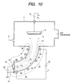
- Fig. 10 is a cross sectional view showing a vacuum arc vapor deposition apparatus which uses the technique 1) above. The vacuum arc vapor deposition apparatus includes a film forming chamber (or vacuum chamber) 2 which is vacuum discharged by a vacuum discharging apparatus (not shown). A
holder 8 for holding asubstrate 6 on which a film is formed is located in the film forming chamber. - In this example, a gas 4, such as inactive gas or reaction gas, is introduced from a gas source (not shown) into the
film forming chamber 2. - A bias voltage VB of -50V to -500V, for example, is applied from a
bias power source 10 to theholder 8 and thesubstrate 6. - The
film forming chamber 2 is connected to a vacuumarc evaporating source 12 through a pipe 28 (deflection pipe) bent about 90° in this example. - The vacuum
arc evaporating source 12 includes acathode 14 mounted on anend plate 29 of thepipe 28 with aninsulating material 20 inserted therebetween. Thecathode 14 is vaporized through vacuum arc discharge occurring between thecathode 14 and thepipe 28 serving also as an anode to produce aplasma 18 containing acathode material 16. An anode electrode may be individually provided. Here, the "cathode material" means material forming thecathode 14. An arc discharging voltage is applied from anarc power source 22 to between thecathode 14 and thepipe 28. Thevacuumarc evaporating source 12 includes a known trigger mechanism, a water cooling mechanism and the like. Those mechanisms are not illustrated in the specification, for simplicity. - A plurality of
magnetic coils 24 are provided around an outer periphery of thepipe 28. The magnetic coils generate a magnetic field for deflecting theplasma 18 produced by the vacuum arcevaporating source 12, and guides (transports) theplasma 18 to the vicinity of thesubstrate 6 in thefilm forming chamber 2. Some ofmagnetic field lines 26 generated by themagnetic coils 24 are roughly illustrated in the figure, and as shown, those magnetic field lines extend substantially along an inner surface of thepipe 28. Thosemagnetic coils 24 are connected in series, and fed with a coil current Ic for generating the magnetic field from acoil power source 30. - The
plasma 18 produced by the vacuumarc evaporating source 12 is bent to substantially along themagnetic field lines 26 and transported to thesubstrate 6. The macro particles emitted from thecathode 14 are electrically neutral or negatively charged in theplasma 18. A mass of the macro particle is considerably large. Accordingly, those particles go straight irrespective of the magnetic field, and hit the inner wall of thebent pipe 28 and hence fail to reach thesubstrate 6. As a result, theplasma 18 little containing the macro particles is led to the vicinity of thesubstrate 6. Thus, it is prevented that the macro particles attach to thesubstrate 6. The apparatus which has themagnetic coils 24,pipe 28 and coil power source 30 (coil power source 40 in Fig. 1) as mentioned above is also called a magnetic filter where attention is put on the macro-particle removing function. - Ions (i.e., ionized cathode material 16) in the
plasma 18 thus transported to near thesubstrate 6 are attracted to thesubstrate 6 under the bias voltage VB and the like, and deposited on the surface of the substrate to form a thin film on the substrate. When a reaction gas which reacts with thecathode material 16 to form a chemical compound is used for the gas 4, a compound thin film may be formed. - When an electron is transported in a uniform magnetic field, as well known, the electron makes a gyrating movement such that it winds round the magnetic field lines, under Lorentz forces given by the following
equation 1. In the equation, q is a charge, v is an electron velocity, and B is a flux density (The same rule applies correspondingly to the description to follow.). -
- Accordingly, in a uniform magnetic field, electrons emitted from two positions P and Q shown in Fig. 11 move along
magnetic field lines 26 uniformly distributed, reach thesubstrate 6, and are incident on positions near positions P1 and Q1 corresponding to the positions P and Q. - Actually, a magnetic field developed by the
magnetic coils 24 is not uniform and has gradients of a magnetic field without exception. For drift of charged particles, such as electrons, in a magnetic field having gradients, reference is made to "Newest Plasma Production Technique", by Yoshinobu Kawai, published by IPC corporation on 5 August, 1991,pages 12 to 21. As described, the charged particle drifts at a drift velocity VD given by the followingequation 2. In the equation, µ is magnetic permeability, ▿B is a gradient (vector) of the magnetic field, and Bv is a magnetic field (vector), and other things are the same as mentioned above. ▿ is a nabla or Hamiltonian operator. -
- The gradient of the magnetic field will be discussed by using an apparatus which transports the
plasma 18 by use of the deflection magnetic field as shown in Fig. 10 (or Fig. 1 to be described later). - A case where the
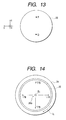
magnetic coil 24 and thepipe 28 are circular in cross section is shown in Figs. 12 to 18. In Figs. 12 to 15, thecathodes cathodes - In this case, the nature of the circular
magnetic coils 24 gives the magnetic field in thepipe 28 such a gradient ▿ B as shown in Fig. 14 that, an intensity of the magnetic field is lowest at thecenter 28a of the pipe inside, and gradually increases toward the outside. In a case where a plurality ofmagnetic coils 24 are disposed while being bent as shown in Fig. 10, for example, the lowest intensity of the magnetic field is located at a position somewhat outwardly shifted from thecenter 28a, actually. - Accordingly, as shown in Figs. 12 and 13,
electrons equation 2. Therefore, the electrons land on thesubstrate 6 at positions shifted in the circumferential direction. The same thing is true for the ions, and hence the plasma drifts, while being shifted in the circumferential direction. - In a case of Figs . 16 and 17 where two vacuum
arc evaporating sources 12 are vertically spaced from each other and arranged along the z-axis,plasma 18 produced by thecathodes substrate 6 while drifting in the circumferential direction. A density distribution of each the plasma produced by thecathodes peaks fringes substrate 6 as shown in a Fig. 18 instance. As shown, those peaks and fringes are located at positions shifted in the circumferential direction frompositions cathodes - A case where the
magnetic coils 24 and thepipe 28 are rectangular in their cross section is illustrated in Figs. 19 to 23. - A magnetic field within the
pipe 28 has such a gradient ▿B as shown in Fig. 20 that an intensity of the magnetic field is lowest at apart 28b slightly closer to the outside than thecenter 28a and gradually increases toward the outside. The gradient ▿B depends on the nature of the rectangularmagnetic coils 24 and the arrangement of the plurality ofmagnetic coils 24 arranged while being bent as shown in Fig. 10 and the like. - As shown in Figs. 12 and 19,
electrons - In a case of Figs. 16 and 22 where two vacuum
arc evaporating sources 12 are vertically spaced from each other and arranged along the z-axis,plasma 18 produced by thecathodes substrate 6 while drifting in the downward and oblique direction. Accordingly, peaks 36a and 36b andfringes substrate 6 as shown in a Fig. 23 instance. As shown, thepeaks fringes positions cathodes - Actually, a shift of the
peak 36a is different from that of the peak 36b. The lateral and downward shifts of the peak 36b on the lower side (as viewed in the z-axis, the same will apply hereinafter.) are greater than that of thepeak 36a on tile upper side. This fact was empirically confirmed. Thepeaks substrate 6. Further, the shifts become larger as a distance of thesubstrate 6 from the vacuumarc evaporating source 12 increases. - Where the
peaks fringes substrate 6 are shifted by the gradient ▿B of the magnetic field, it is difficult to form a film on thesubstrate 6 as desired. The shift will deteriorate the uniformity of the thickness distribution on the surface of thesubstrate 6. When comparing with a case where themagnetic coils 24 and thepipe 28 are circular in cross section, in a case where the where themagnetic coils 24 and thepipe 28 are rectangular in cross section, thepeaks substrate 6 ad the vacuumarc evaporating source 12 increases. Accordingly, the uniformity of the thickness distribution on the surface of thesubstrate 6 is more deteriorated. - Accordingly, an object of the invention is to provide a vacuum arc vapor deposition apparatus and a vacuum arc vapor deposition method which can prevent degradation of the uniformity of a film thickness distribution on a surface of a substrate, which is caused by the drift of a plasma in a magnetic field developed by a magnetic coil.
- In order to accomplish the object above, the following means are adopted. According to the present invention, there is provided a vacuum arc vapor deposition apparatus comprising:
a film forming chamber containing a substrate and being vacuum discharged; a vacuum arc evaporating source for producing a plasma containing a cathode material by vaporizing a cathode by vacuum arc discharge; a magnetic coil for generating a magnetic field for deflecting or converging the plasma produced by the vacuum arc evaporating source, and guiding the plasma to the vicinity of the substrate within the film forming chamber; a coil power source for feeding a coil current for generating the magnetic field to the magnetic coil, the coil power source reversing a flowing direction of the coil current fed to the magnetic coil; and a control unit for controlling the coil power source to reverse the flowing direction of the coil current fed to the magnetic coil. - The plasma is guided (transported) to the vicinity of the substrate by the magnetic field developed by the magnetic coils before and after the flowing direction of the coil current fed to the magnetic coils is reversed. The reason for this is that so long as the magnetic field exists, the plasma is guided by the magnetic field.
- When the flowing direction of the current fed to the magnetic coils is reversed, the gradient ▿B of the magnetic field remains unchanged, but the direction of the vector of magnetic field Bv is reversed. As seen also from the
equation 2, the drift velocity VD acting on the plasma to be transported is reversed in its direction. - The phenomenon, already stated, that the peak positions of the thickness distribution on the substrate surface are shifted by the drift of the plasma being under transportation, appears in the inverted state on the substrate surface when the flowing direction of the coil current is reversed. This inversion reduces the non-uniformity of the film thickness distribution, thereby preventing the deterioration of the uniformity of the film thickness distribution on the substrate surface. The result is that a film may be formed more uniformly over a broader area on the substrate.
-
- Fig. 1 is a diagram showing a vacuum arc vapor deposition apparatus according to the present invention;
- Fig. 2 shows, in a view in the direction C - C in Fig. 1, an arrangement of cathodes in two vacuum arc evaporating sources in a case where a magnetic coil and a pipe are rectangular in cross section;
- Fig. 3 shows, in a view in the direction D - D in Fig. 1, drift directions of electrons in a magnetic field by the magnetic coil in Fig. 1, before the coil current is reversed in its flowing direction, in a case where a magnetic coil and a pipe are rectangular in cross section;
- Fig. 4 shows, in a view in the direction D - D in Fig. 1, drift directions of electrons in a magnetic field by the magnetic coil in Fig. 1, after the coil current is reversed in its flowing direction, in a case where a magnetic coil and a pipe are rectangular in cross section;
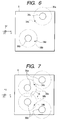
- Fig. 5 is a diagram showing film thickness distributions on a surface of a film formed substrate by the cathodes in Fig. 2 before the coil current is reversed in its flowing direction;
- Fig. 6 is a diagram showing film thickness distributions on a surface of a film formed substrate by the cathodes in Fig. 2 after the coil current is reversed in its flowing direction;
- Fig. 7 is a diagram showing film thickness distributions when the Figs. 5 and 6 distributions are superimposed one on the other;
- Fig. 8 is a diagram showing a case where two thickness meters are located close to the periphery of the substrate;
- Fig. 9 is a diagram showing a case where two ion current probes are located close to the periphery of the substrate;
- Fig. 10 is a cross sectional view showing a vacuum arc vapor deposition apparatus in related art;
- Fig. 11 is a diagram showing electron motions in a uniform magnetic field;
- Fig. 12 is a diagram showing a portion of the magnetic coil of the Figs. 1 and 10 apparatus;
- Fig. 13 is a diagram showing a cross section of the Fig. 12 structure as viewed in a direction C - C in a case where a magnetic coil and a pipe are circular in cross section;
- Fig. 14 is a diagram showing a gradation of a magnetic field in a cross section of the Fig. 12 structure as viewed in a direction D - D in a case where a magnetic coil and a pipe are circular in cross section;
- Fig. 15 is a diagram showing drift directions of electrons in a magnetic field developed by the Fig. 14 magnetic coil;
- Fig. 16 is a diagram showing a structure of each of the Figs. 1 and 10, which ranges from the cathode to the substrate;
- Fig. 17 shows, in a view in the direction of C - C in Fig. 16, an arrangement of cathodes in a case where a magnetic coil and a pipe are circular in cross section;
- Fig. 18 is a diagram showing film thickness distributions on a surface of a film formed substrate, which are caused by the cathodes in Fig. 17;
- Fig. 19 is a diagram showing a cross section of the Fig. 12 structure as viewed in a direction C - C in a case where a magnetic coil and a pipe are rectangular in cross section;
- Fig. 20 is a diagram showing a gradation of a magnetic field in a cross section of the Fig. 12 structure as viewed in a direction D - D in a case where a magnetic coil and a pipe are rectangular in cross section;
- Fig. 21 is a diagram showing drift directions of electrons in a magnetic field developed by the Fig. 20 magnetic coil;
- Fig. 22 shows, in a view in the direction of C - C in Fig. 16, an arrangement of cathodes in a case where a magnetic coil and a pipe are rectangular in cross section; and
- Fig. 23 is a diagram showing film thickness distributions on a surface of a film formed substrate, which are caused by the cathodes in Fig. 22.
-
- Fig. 1 is a diagram exemplarily showing a vacuum arc vapor deposition apparatus according to the present invention. Fig. 2 shows, in a view in the direction C-C in Fig. 1, an arrangement of cathodes in two vacuum arc evaporating sources in a case where a magnetic coil and pipe are rectangular in cross section. Fig. 2 is the same diagram as Fig. 22 described above. In the figures, like or same portions used in Figs. 10 to 23 are designated by like reference numerals. Description will be given placing emphasis on the differences of the embodiment from the related art apparatus.
- The vacuum arc vapor deposition apparatus shown in Fig. 1 comprises a
coil power source 40 and acontrol unit 42. Thecoil power source 40 is used in place of the related art coilDC power source 30 and reverses the flowing direction of coil current Ic, which flow through a plurality ofmagnetic coils 24,. Thecontrol unit 42 controls thecoil power source 40 to reverse the flowing direction of the coil current Ic flowing through eachmagnetic coil 24. - The
coil power source 40 may be a bipolar power source capable of feeding bipolar current or may be a combination of two DC power sources; one feeds a positive current, and the other feeds a negative current. - In the vacuum arc vapor deposition apparatus, two vacuum
arc evaporating sources 12 are arranged along the z-axis while being vertically separated from each other. - Each of
magnetic coils 24 and thepipe 28 may be circular in cross section as in the case described above. In the cases of Figs. 2 to 7, the cross section configuration of them is rectangular. - The
plasma 18 produced by the vacuumarc evaporating source 12 is guided (transported) to the vicinity of thesubstrate 6 in thefilm forming chamber 2 before and after the coil current Ic flowing through themagnetic coils 24 is reversed in its flowing direction. The reason for this is that so long as the magnetic field exists, the plasma is guided by the magnetic field. - When the coil current Ic flows through each
magnetic coil 24 in the clockwise direction as viewed from the vacuumarc evaporating source 12,electrons cathodes arc evaporating sources 12 drift obliquely and downward at a drift velocity VD as shown in Fig. 3. With the drift of the electrons, theplasma 18, which is produced in the vicinity of thecathodes peak positions fringes substrate 6 appear at positions shifted obliquely and downward as shown in Fig. 5. Figs. 3 and 5 respectively correspond to Figs. 21 and 23 mentioned above. The reason why the drift velocity VD and the thickness distribution are shifted are as already described in detail. - When the flowing direction of the coil current Ic fed to
magnetic coils 24 is reversed, i.e., in the counterclockwise direction as shown in Fig. 4, the gradient ▿B of the magnetic field developed by themagnetic coils 24 remains unchanged, but the direction of the vector of magnetic field Bv is reversed. As seen also from theequation 2, the drift velocity VD acting on theelectrons plasma 18, which is produced in the vicinity of thecathodes - As a result, the phenomenon, already stated, that the
peak positions fringes peaks cathodes positions cathodes - By reversing the flowing direction of the coil current Ic, the thickness distributions shown in Figs. 5 and 6 are superimposed one on the other into a film thickness distribution as shown in Fig. 7. Thus, peaks 36a and 36b and the
fringes substrate 6 in a dispersing fashion. When a time t1 that the coil current Ic flows clockwise is selected to be equal to a time t2 that the current flows counter clockwise, peaks whose magnitudes (film thickness) are substantially equal appear at four positions dispersley. With the dispersion of the peak positions, non-uniformity of the thickness distribution on the surface of thesubstrate 6 is reduced. Thus, deterioration of the uniformity of the film thickness distribution on the surface of thesubstrate 6 can be prevented by the drift of theplasma 18 in the magnetic field generated by themagnetic coils 24. As a result, a film may be formed uniformly on a broad area on thesubstrate 6. - The
substrate 6 and theholder 8 holding it may be rotated about the center of thesubstrate 6 in, for example, a direction of an arrow "R" (or its reverse direction), as shown in Figs. 1 and 7. By so doing, the non-uniformity of the film thickness distribution is reduced through the rotation of thesubstrate 6, so that the film thickness on thesubstrate 6 is more uniform. - The
control unit 42 controls thecoil power source 40 to reverse the flowing direction of the coil current Ic after a predetermined time elapses. The reversing operation may be performed one time; however, it is preferable to repeat the reversing operation at predetermined time intervals. If so doing, the reducing of the non-uniformity of the thickness distribution caused by reversing the coil current Ic is repeated, and hence, the thickness distribution is more uniform. - The time t1 of flowing the coil current Ic in the predetermined direction and the time t2 of flowing the same in the reverse direction may be selected to be equal with each other. Those times may be selected to be different so as to enhance the uniformity of the film thickness distribution by reducing the non-uniformity of the film thickness distribution in a more sophisticated manner.
- It is preferable to repeat the reversing operation of the coil current Ic direction at short time intervals. The reason for this is that it is possible to reduce the concentration of thermal stress on the
substrate 6 by ions in theplasma 18 which are incident on the substrate, and hence the thermal stress concentration on the substrate is reduced. One of the preferable ways is to reverse the flowing direction of the coil current Ic at a time interval, which is integer times as long as a time taken for one rotation of thesubstrate 6. In a specific example, where the time taken for one rotation of thesubstrate 6 is 5 seconds, the flowing direction of the coil current Ic is reversed at a time interval of 10 seconds. - To more improve the uniformity of the film thickness distribution on the surface of the
substrate 6, the following thickness or ion current detecting unit may be employed. - In the vacuum arc vapor deposition device shown in Fig. 8, a plurality of
thickness meters 44 each for measuring a thickness of a film formed by theplasma 18 are disposed in the vicinity of thesubstrate 6. Specifically, in this instance, twothickness meters 44 are disposed close to and above and below thesubstrate 6. Thecontrol unit 42 performs the control for reversing the flowing direction of the coil current Ic when a difference between film thickness values as measured by the twothickness meters 44 exceeds a predetermined value. - Where the thickness detecting unit is employed, the vacuum arc vapor deposition device performs the control for reversing the flowing direction of the coil current Ic for reducing the non-uniformity of the thickness distribution on the surface of the
substrate 6 while monitoring the film thickness on the surface of the film formedsubstrate 6 at plural positions close to the periphery of thesubstrate 6. Accordingly, the uniformity of the thickness distribution on the surface of thesubstrate 6 is more improved. - In the vacuum arc vapor deposition device shown in Fig. 9, a plurality of ion current probes 46 are provided in the vicinity of the
substrate 6, for measuring ion currents II which flows when ions in theplasma 18 are incident thereon. More specifically, in this instance, the two ion current probes 46 are disposed above and below and near thesubstrate 6. Additionally, twocurrent integrators 50 for integrating ion currents II flowing through the ion current probes 46 are provided. The ion current probes 46 may be kept at ground potential. To exactly measure ion currents II, it is preferable that abias power source 48 is provided, and it is negatively biased, as in the instance. Thecontrol unit 42 performs the control for reversing the flowing direction of the coil current Ic when adifference between current values integrated by the twocurrent integrators 50 exceeds a predetermined value. - The reason why a film is formed on the
substrate 6 by guiding theplasma 18 to the vicinity of thesubstrate 6, is that ions (ionized cathode material 16) in theplasma 18 are incident on thesubstrate 6. A correlation is present between the amount of the incident ions and the film thickness. The amount of the incident ions is measured by using the integrated value of the ion currents II. - Accordingly, by using the ion current detecting unit as mentioned above, the vacuum arc vapor deposition device performs the control for reversing the flowing direction of the coil current Ic for reducing the non-uniformity of the amount of the incident ions while monitoring the amount of incident ions on the
substrate 6 at plural locations close to the periphery of thesubstrate 6. This further improves the uniformity of the thickness distribution on the surface of thesubstrate 6. - Also in the case where the
magnetic coil 24 and thepipe 28 are circular in cross section, theplasma 18 drifts by the gradient ▿B of the magnetic field, thereby impairing the uniformity of the thickness distribution on the surface of thesubstrate 6, as described with reference to the Figs. 13 to 15, 17, and 18. In this case, however, the direction of the drift of theplasma 18 may be reversed by reversing the flowing direction of the coil current Ic. With this, the non-uniformity of the thickness distribution may be reduced. Specifically, the degradation of the uniformity of the thickness distribution on the surface of thesubstrate 6 is prevented by the reversed drift of theplasma 18 in the magnetic field developed by themagnetic coil 24. - In the embodiments mentioned above, a deflection magnetic field is developed by the plurality of
magnetic coils 24, and theplasma 18 is deflected and transported. If required, theplasma 18 may be guide to the vicinity of thesubstrate 6 by the magnetic field, while not defected by the magnetic field. In this case, the macro particles are made fine by converging theplasma 18 to increase the density of the plasma by one or a plurality of magnetic coils, as described above. As long as theplasma 18 is transported by using the magnetic field developed by the magnetic coil, the above-mentioned gradient ▿B of the magnetic field exists, and it causes theplasma 18 to drift in the predetermined direction. This deteriorates the uniformity of the thickness distribution on the surface of thesubstrate 6. Similarly, in this case, the direction of the drift of theplasma 18 may be reversed by reversing the flowing direction of the coil current Ic. Accordingly, the non-uniformity of the thickness distribution may be reduced. - The present invention thus constructed has the following useful effects.
- The vacuum arc vapor deposition device of the invention includes the coil power source and the control unit. Accordingly, the flowing direction of the coil current fed to the magnetic coils is reversed. As a result, the phenomenon that the peak positions of the thickness distribution on the substrate surface are shifted by the drift of the plasma being under transportation, appears in the inverted state on the substrate surface when the coil current fed to the magnetic coils is reversed in its flowing direction. This reversion reduces the non-uniformity of the film thickness distribution, thereby preventing the deterioration of the uniformity of the film thickness distribution on the substrate surface. The result is that a film may be formed more uniformly over a broader area on the substrate.
- When a plurality of vacuum arc evaporating sources are provided, and the magnetic coils generate a deflection magnetic field, the non-uniformity of the thickness distribution by the drift of the plasma is easy to occur. In this case, the effect of improving the non-uniformity of the film thickness distribution is more remarkable when the coil power source and the control unit are provided so that the flowing direction of the coil current fed to the magnetic coils is reversed.
- In the vacuum arc vapor deposition device of the invention, the reducing operation for the non-uniformity of the thickness distribution by reversing the flowing direction of the coil current may be carried out repeatedly. Therefore, the uniformity of the thickness distribution is improved.
- The vacuum arc vapor deposition device of the invention may perform the control for reversing the flowing direction of the coil current to reduce the non-uniformity of the thickness distribution while monitoring the film thickness on the surface of the film formed substrate at a plurality of locations close to the periphery of the substrate. Accordingly, the uniformity of the thickness distribution on the surface of the substrate is improved.
- The vacuum arc vapor deposition device of the invention may perform the control for reversing the flowing direction of the coil current to reduce the non-uniformity of the amount of the incident ions while monitoring the amount of incident ions on the substrate in a plurality of locations close to the periphery of the substrate. Accordingly, the uniformity of the thickness distribution on the surface of the substrate is improved.
Claims (12)
- A vacuum arc vapor deposition apparatus comprising;a film forming chamber containing a substrate and being vacuum discharged;a vacuum arc evaporating source for producing a plasma containing a cathode material by vaporizing a cathode by vacuum arc discharge;a magnetic coil for generating a magnetic field for deflecting or converging said plasma produced by said vacuum arc evaporating source, and guiding said plasma to the vicinity of said substrate within said film forming chamber;a coil power source for feeding a coil current for generating said magnetic field to said magnetic coil, said coil power source reversing a flowing direction of the coil current fed to said magnetic coil; anda control unit for controlling said coil power source to reverse the flowing direction of the coil current fed to said magnetic coil.
- The vacuum arc vapor deposition apparatus according to claim 1, wherein a plurality of vacuum arc evaporating sources are provided, and said magnetic coil generates a deflection magnetic field for deflecting said plasma.
- The vacuum arc vapor deposition apparatus according to claim 1, wherein said control unit performs a control for repeatedly reversing the flowing direction of said coil current every predetermined time.
- The vacuum arc vapor deposition apparatus according to claim 1, further comprising:wherein said control unit performs the control for reversing the flowing direction of the coil current when a difference between film thickness values as measured by said plurality of thickness detecting units exceeds a predetermined value.a plurality of thickness detecting units, disposed in the vicinity of said substrate, each for measuring a thickness of a film formed by said plasma,
- The vacuum arc vapor deposition apparatus according to claim 1, further comprising:wherein said control unit performs the control for reversing the flowing direction of the coil current when a difference between current values integrated by said plurality of said current integrators exceeds a predetermined value.a plurality of ion current detecting units, disposed in the vicinity of said substrate, for measuring ion currents which flows when ions in said plasma are incident thereon; anda plurality of current integrators for integrating ion currents flowing through said ion current detecting units,
- The vacuum arc vapor deposition apparatus according to claim 1, wherein the substrate rotates about its center.
- The vacuum arc vapor deposition apparatus according to claim 6, wherein the flowing direction of the coil current is reversed at a time interval which is integer times as long as a time taken for one rotation of the substrate.
- The vacuum arc vapor deposition apparatus according to claim 1, wherein said control unit controls a time of flowing the coil current in a predetermined direction and a time of flowing the coil current in a reverse direction to be equal with each other.
- A vacuum arc vapor deposition method comprising;producing a plasma containing a cathode material by vaporizing a cathode by vacuum arc discharge;feeding a coil current for generating a magnetic field to a magnetic coil to deflect or converge said plasma thus produced and guide said plasma to the vicinity of a substrate; andreversing a flowing direction of the coil current fed to the magnetic coil.
- The vacuum arc vapor deposition method according to claim 9, wherein the flowing direction of said coil current is repeatedly reversed every predetermined time.
- The vacuum arc vapor deposition method according to claim 9, further comprising:wherein the flowing direction of the coil current is reversed when a difference between film thickness values thus measured exceeds a predetermined value.measuring a thickness of a film formed by said plasma at a plurality of points in the vicinity of the substrate,
- The vacuum arc vapor deposition method according to claim 9, further comprising:wherein the flowing direction of the coil current is reversed when a difference between current values thus measured exceeds a predetermined value.measuring ion currents at a plurality of points in the vicinity of the substrate,
Applications Claiming Priority (2)
| Application Number | Priority Date | Filing Date | Title |
|---|---|---|---|
| JP2001095815A JP4085593B2 (en) | 2001-03-29 | 2001-03-29 | Vacuum arc evaporation system |
| JP2001095815 | 2001-03-29 |
Publications (2)
| Publication Number | Publication Date |
|---|---|
| EP1245694A1 true EP1245694A1 (en) | 2002-10-02 |
| EP1245694B1 EP1245694B1 (en) | 2004-08-25 |
Family
ID=18949820
Family Applications (1)
| Application Number | Title | Priority Date | Filing Date |
|---|---|---|---|
| EP02007409A Expired - Fee Related EP1245694B1 (en) | 2001-03-29 | 2002-03-28 | Vacuum arc vapor deposition apparatus and vacuum arc vapor deposition method |
Country Status (6)
| Country | Link |
|---|---|
| US (2) | US6692623B2 (en) |
| EP (1) | EP1245694B1 (en) |
| JP (1) | JP4085593B2 (en) |
| KR (1) | KR100496464B1 (en) |
| DE (1) | DE60201044T2 (en) |
| HK (1) | HK1048832B (en) |
Cited By (20)
| Publication number | Priority date | Publication date | Assignee | Title |
|---|---|---|---|---|
| EP1449934A2 (en) * | 2002-12-27 | 2004-08-25 | Nissin Electric Co., Ltd. | Vacuum arc vapor deposition apparatus |
| US9272095B2 (en) | 2011-04-01 | 2016-03-01 | Sio2 Medical Products, Inc. | Vessels, contact surfaces, and coating and inspection apparatus and methods |
| US9458536B2 (en) | 2009-07-02 | 2016-10-04 | Sio2 Medical Products, Inc. | PECVD coating methods for capped syringes, cartridges and other articles |
| US9545360B2 (en) | 2009-05-13 | 2017-01-17 | Sio2 Medical Products, Inc. | Saccharide protective coating for pharmaceutical package |
| US9554968B2 (en) | 2013-03-11 | 2017-01-31 | Sio2 Medical Products, Inc. | Trilayer coated pharmaceutical packaging |
| US9572526B2 (en) | 2009-05-13 | 2017-02-21 | Sio2 Medical Products, Inc. | Apparatus and method for transporting a vessel to and from a PECVD processing station |
| US9664626B2 (en) | 2012-11-01 | 2017-05-30 | Sio2 Medical Products, Inc. | Coating inspection method |
| US9662450B2 (en) | 2013-03-01 | 2017-05-30 | Sio2 Medical Products, Inc. | Plasma or CVD pre-treatment for lubricated pharmaceutical package, coating process and apparatus |
| US9764093B2 (en) | 2012-11-30 | 2017-09-19 | Sio2 Medical Products, Inc. | Controlling the uniformity of PECVD deposition |
| US9863042B2 (en) | 2013-03-15 | 2018-01-09 | Sio2 Medical Products, Inc. | PECVD lubricity vessel coating, coating process and apparatus providing different power levels in two phases |
| US9878101B2 (en) | 2010-11-12 | 2018-01-30 | Sio2 Medical Products, Inc. | Cyclic olefin polymer vessels and vessel coating methods |
| US9903782B2 (en) | 2012-11-16 | 2018-02-27 | Sio2 Medical Products, Inc. | Method and apparatus for detecting rapid barrier coating integrity characteristics |
| US9937099B2 (en) | 2013-03-11 | 2018-04-10 | Sio2 Medical Products, Inc. | Trilayer coated pharmaceutical packaging with low oxygen transmission rate |
| US10189603B2 (en) | 2011-11-11 | 2019-01-29 | Sio2 Medical Products, Inc. | Passivation, pH protective or lubricity coating for pharmaceutical package, coating process and apparatus |
| US10201660B2 (en) | 2012-11-30 | 2019-02-12 | Sio2 Medical Products, Inc. | Controlling the uniformity of PECVD deposition on medical syringes, cartridges, and the like |
| US11066745B2 (en) | 2014-03-28 | 2021-07-20 | Sio2 Medical Products, Inc. | Antistatic coatings for plastic vessels |
| US11077233B2 (en) | 2015-08-18 | 2021-08-03 | Sio2 Medical Products, Inc. | Pharmaceutical and other packaging with low oxygen transmission rate |
| US11116695B2 (en) | 2011-11-11 | 2021-09-14 | Sio2 Medical Products, Inc. | Blood sample collection tube |
| WO2022128719A1 (en) * | 2020-12-15 | 2022-06-23 | Fraunhofer-Gesellschaft zur Förderung der angewandten Forschung e.V. | Device for forming amorphous carbon layers on component surfaces having reduced surface roughness |
| US11624115B2 (en) | 2010-05-12 | 2023-04-11 | Sio2 Medical Products, Inc. | Syringe with PECVD lubrication |
Families Citing this family (18)
| Publication number | Priority date | Publication date | Assignee | Title |
|---|---|---|---|---|
| US20040134770A1 (en) * | 2002-11-15 | 2004-07-15 | Petersen John H | Ionic plasma deposition apparatus |
| US8066854B2 (en) * | 2002-12-18 | 2011-11-29 | Metascape Llc | Antimicrobial coating methods |
| JP2006515387A (en) * | 2002-12-18 | 2006-05-25 | アイオニック フュージョン コーポレイション | Ionic plasma deposition of anti-microbial surfaces and anti-microbial surfaces obtained therefrom |
| US7509734B2 (en) * | 2003-03-03 | 2009-03-31 | United Technologies Corporation | Repairing turbine element |
| JP4438326B2 (en) * | 2003-06-13 | 2010-03-24 | 日新電機株式会社 | Deflection magnetic field type vacuum arc deposition system |
| US20080003377A1 (en) * | 2006-06-30 | 2008-01-03 | The Board Of Regents Of The Nevada System Of Higher Ed. On Behalf Of The Unlv | Transparent vacuum system |
| JP4660452B2 (en) * | 2006-09-30 | 2011-03-30 | 株式会社フェローテック | Expanded tube plasma generator |
| US7872244B2 (en) * | 2007-08-08 | 2011-01-18 | Asml Netherlands B.V. | Lithographic apparatus and device manufacturing method |
| JP4955027B2 (en) * | 2009-04-02 | 2012-06-20 | クリーン・テクノロジー株式会社 | Control method of plasma by magnetic field in exhaust gas treatment device |
| JP5644085B2 (en) * | 2009-06-10 | 2014-12-24 | 富士通株式会社 | Film forming apparatus and film forming method |
| KR101036676B1 (en) * | 2009-07-31 | 2011-05-23 | 한국염색기술연구소 | Device for producing fuel of dyeing wastewater sludge in coal-fired power utility boiler plant and method thereof |
| JP5606777B2 (en) * | 2010-04-22 | 2014-10-15 | 株式会社フェローテック | Plasma flow generation method, plasma processing method, plasma generator, and plasma processing apparatus |
| CN102776479A (en) * | 2011-05-09 | 2012-11-14 | 无锡尚德太阳能电力有限公司 | Preparation device and method for film |
| US9153422B2 (en) | 2011-08-02 | 2015-10-06 | Envaerospace, Inc. | Arc PVD plasma source and method of deposition of nanoimplanted coatings |
| US9793098B2 (en) | 2012-09-14 | 2017-10-17 | Vapor Technologies, Inc. | Low pressure arc plasma immersion coating vapor deposition and ion treatment |
| US10056237B2 (en) | 2012-09-14 | 2018-08-21 | Vapor Technologies, Inc. | Low pressure arc plasma immersion coating vapor deposition and ion treatment |
| US9721760B2 (en) * | 2013-05-16 | 2017-08-01 | Applied Materials, Inc. | Electron beam plasma source with reduced metal contamination |
| US9564297B2 (en) | 2013-05-16 | 2017-02-07 | Applied Materials, Inc. | Electron beam plasma source with remote radical source |
Citations (6)
| Publication number | Priority date | Publication date | Assignee | Title |
|---|---|---|---|---|
| US4724058A (en) * | 1984-08-13 | 1988-02-09 | Vac-Tec Systems, Inc. | Method and apparatus for arc evaporating large area targets |
| US5279723A (en) * | 1992-07-30 | 1994-01-18 | As Represented By The United States Department Of Energy | Filtered cathodic arc source |
| US5840163A (en) * | 1994-04-25 | 1998-11-24 | Vapor Technologies, Inc. | Rectangular vacuum-arc plasma source |
| EP0926699A1 (en) * | 1997-10-22 | 1999-06-30 | Nissin Electric Co., Ltd. | Method and apparatus for deflecting charged particles |
| JP2000034561A (en) * | 1998-07-17 | 2000-02-02 | Mitsubishi Materials Corp | Formation of metallic compound thin film small in coarse droplet number by arc type ion plating method |
| JP2001003160A (en) * | 1999-06-18 | 2001-01-09 | Nissin Electric Co Ltd | Formation of film and device therefor |
Family Cites Families (2)
| Publication number | Priority date | Publication date | Assignee | Title |
|---|---|---|---|---|
| US5298136A (en) * | 1987-08-18 | 1994-03-29 | Regents Of The University Of Minnesota | Steered arc coating with thick targets |
| KR100230279B1 (en) | 1997-03-31 | 1999-11-15 | 윤종용 | Coating apparatus by using cathodic arc discharge |
-
2001
- 2001-03-29 JP JP2001095815A patent/JP4085593B2/en not_active Expired - Fee Related
-
2002
- 2002-03-28 US US10/107,363 patent/US6692623B2/en not_active Expired - Fee Related
- 2002-03-28 EP EP02007409A patent/EP1245694B1/en not_active Expired - Fee Related
- 2002-03-28 DE DE60201044T patent/DE60201044T2/en not_active Expired - Lifetime
- 2002-03-29 KR KR10-2002-0017207A patent/KR100496464B1/en not_active IP Right Cessation
-
2003
- 2003-02-11 HK HK03100983.6A patent/HK1048832B/en not_active IP Right Cessation
- 2003-09-10 US US10/658,410 patent/US6866753B2/en not_active Expired - Fee Related
Patent Citations (6)
| Publication number | Priority date | Publication date | Assignee | Title |
|---|---|---|---|---|
| US4724058A (en) * | 1984-08-13 | 1988-02-09 | Vac-Tec Systems, Inc. | Method and apparatus for arc evaporating large area targets |
| US5279723A (en) * | 1992-07-30 | 1994-01-18 | As Represented By The United States Department Of Energy | Filtered cathodic arc source |
| US5840163A (en) * | 1994-04-25 | 1998-11-24 | Vapor Technologies, Inc. | Rectangular vacuum-arc plasma source |
| EP0926699A1 (en) * | 1997-10-22 | 1999-06-30 | Nissin Electric Co., Ltd. | Method and apparatus for deflecting charged particles |
| JP2000034561A (en) * | 1998-07-17 | 2000-02-02 | Mitsubishi Materials Corp | Formation of metallic compound thin film small in coarse droplet number by arc type ion plating method |
| JP2001003160A (en) * | 1999-06-18 | 2001-01-09 | Nissin Electric Co Ltd | Formation of film and device therefor |
Non-Patent Citations (2)
| Title |
|---|
| PATENT ABSTRACTS OF JAPAN vol. 2000, no. 05 14 September 2000 (2000-09-14) * |
| PATENT ABSTRACTS OF JAPAN vol. 2000, no. 16 8 May 2001 (2001-05-08) * |
Cited By (39)
| Publication number | Priority date | Publication date | Assignee | Title |
|---|---|---|---|---|
| EP1449934A2 (en) * | 2002-12-27 | 2004-08-25 | Nissin Electric Co., Ltd. | Vacuum arc vapor deposition apparatus |
| EP1449934A3 (en) * | 2002-12-27 | 2006-02-01 | Nissin Electric Co., Ltd. | Vacuum arc vapor deposition apparatus |
| US7060167B2 (en) | 2002-12-27 | 2006-06-13 | Nissin Electrci Co., Ltd | Vacuum arc vapor deposition apparatus |
| EP1801259A2 (en) * | 2002-12-27 | 2007-06-27 | Nissin Electric Co., Ltd. | Vacuum arc vapor deposition apparatus |
| EP1801259A3 (en) * | 2002-12-27 | 2007-07-04 | Nissin Electric Co., Ltd. | Vacuum arc vapor deposition apparatus |
| US9572526B2 (en) | 2009-05-13 | 2017-02-21 | Sio2 Medical Products, Inc. | Apparatus and method for transporting a vessel to and from a PECVD processing station |
| US9545360B2 (en) | 2009-05-13 | 2017-01-17 | Sio2 Medical Products, Inc. | Saccharide protective coating for pharmaceutical package |
| US10537273B2 (en) | 2009-05-13 | 2020-01-21 | Sio2 Medical Products, Inc. | Syringe with PECVD lubricity layer |
| US10390744B2 (en) | 2009-05-13 | 2019-08-27 | Sio2 Medical Products, Inc. | Syringe with PECVD lubricity layer, apparatus and method for transporting a vessel to and from a PECVD processing station, and double wall plastic vessel |
| US9458536B2 (en) | 2009-07-02 | 2016-10-04 | Sio2 Medical Products, Inc. | PECVD coating methods for capped syringes, cartridges and other articles |
| US11624115B2 (en) | 2010-05-12 | 2023-04-11 | Sio2 Medical Products, Inc. | Syringe with PECVD lubrication |
| US9878101B2 (en) | 2010-11-12 | 2018-01-30 | Sio2 Medical Products, Inc. | Cyclic olefin polymer vessels and vessel coating methods |
| US11123491B2 (en) | 2010-11-12 | 2021-09-21 | Sio2 Medical Products, Inc. | Cyclic olefin polymer vessels and vessel coating methods |
| US9272095B2 (en) | 2011-04-01 | 2016-03-01 | Sio2 Medical Products, Inc. | Vessels, contact surfaces, and coating and inspection apparatus and methods |
| US10189603B2 (en) | 2011-11-11 | 2019-01-29 | Sio2 Medical Products, Inc. | Passivation, pH protective or lubricity coating for pharmaceutical package, coating process and apparatus |
| US10577154B2 (en) | 2011-11-11 | 2020-03-03 | Sio2 Medical Products, Inc. | Passivation, pH protective or lubricity coating for pharmaceutical package, coating process and apparatus |
| US11884446B2 (en) | 2011-11-11 | 2024-01-30 | Sio2 Medical Products, Inc. | Passivation, pH protective or lubricity coating for pharmaceutical package, coating process and apparatus |
| US11148856B2 (en) | 2011-11-11 | 2021-10-19 | Sio2 Medical Products, Inc. | Passivation, pH protective or lubricity coating for pharmaceutical package, coating process and apparatus |
| US11724860B2 (en) | 2011-11-11 | 2023-08-15 | Sio2 Medical Products, Inc. | Passivation, pH protective or lubricity coating for pharmaceutical package, coating process and apparatus |
| US11116695B2 (en) | 2011-11-11 | 2021-09-14 | Sio2 Medical Products, Inc. | Blood sample collection tube |
| US9664626B2 (en) | 2012-11-01 | 2017-05-30 | Sio2 Medical Products, Inc. | Coating inspection method |
| US9903782B2 (en) | 2012-11-16 | 2018-02-27 | Sio2 Medical Products, Inc. | Method and apparatus for detecting rapid barrier coating integrity characteristics |
| US10363370B2 (en) | 2012-11-30 | 2019-07-30 | Sio2 Medical Products, Inc. | Controlling the uniformity of PECVD deposition |
| US9764093B2 (en) | 2012-11-30 | 2017-09-19 | Sio2 Medical Products, Inc. | Controlling the uniformity of PECVD deposition |
| US11406765B2 (en) | 2012-11-30 | 2022-08-09 | Sio2 Medical Products, Inc. | Controlling the uniformity of PECVD deposition |
| US10201660B2 (en) | 2012-11-30 | 2019-02-12 | Sio2 Medical Products, Inc. | Controlling the uniformity of PECVD deposition on medical syringes, cartridges, and the like |
| US9662450B2 (en) | 2013-03-01 | 2017-05-30 | Sio2 Medical Products, Inc. | Plasma or CVD pre-treatment for lubricated pharmaceutical package, coating process and apparatus |
| US10537494B2 (en) | 2013-03-11 | 2020-01-21 | Sio2 Medical Products, Inc. | Trilayer coated blood collection tube with low oxygen transmission rate |
| US11684546B2 (en) | 2013-03-11 | 2023-06-27 | Sio2 Medical Products, Inc. | PECVD coated pharmaceutical packaging |
| US11298293B2 (en) | 2013-03-11 | 2022-04-12 | Sio2 Medical Products, Inc. | PECVD coated pharmaceutical packaging |
| US11344473B2 (en) | 2013-03-11 | 2022-05-31 | SiO2Medical Products, Inc. | Coated packaging |
| US10016338B2 (en) | 2013-03-11 | 2018-07-10 | Sio2 Medical Products, Inc. | Trilayer coated pharmaceutical packaging |
| US9937099B2 (en) | 2013-03-11 | 2018-04-10 | Sio2 Medical Products, Inc. | Trilayer coated pharmaceutical packaging with low oxygen transmission rate |
| US9554968B2 (en) | 2013-03-11 | 2017-01-31 | Sio2 Medical Products, Inc. | Trilayer coated pharmaceutical packaging |
| US10912714B2 (en) | 2013-03-11 | 2021-02-09 | Sio2 Medical Products, Inc. | PECVD coated pharmaceutical packaging |
| US9863042B2 (en) | 2013-03-15 | 2018-01-09 | Sio2 Medical Products, Inc. | PECVD lubricity vessel coating, coating process and apparatus providing different power levels in two phases |
| US11066745B2 (en) | 2014-03-28 | 2021-07-20 | Sio2 Medical Products, Inc. | Antistatic coatings for plastic vessels |
| US11077233B2 (en) | 2015-08-18 | 2021-08-03 | Sio2 Medical Products, Inc. | Pharmaceutical and other packaging with low oxygen transmission rate |
| WO2022128719A1 (en) * | 2020-12-15 | 2022-06-23 | Fraunhofer-Gesellschaft zur Förderung der angewandten Forschung e.V. | Device for forming amorphous carbon layers on component surfaces having reduced surface roughness |
Also Published As
| Publication number | Publication date |
|---|---|
| KR20020077216A (en) | 2002-10-11 |
| US20040045812A1 (en) | 2004-03-11 |
| DE60201044D1 (en) | 2004-09-30 |
| HK1048832A1 (en) | 2003-04-17 |
| US20020157609A1 (en) | 2002-10-31 |
| US6692623B2 (en) | 2004-02-17 |
| US6866753B2 (en) | 2005-03-15 |
| KR100496464B1 (en) | 2005-06-20 |
| EP1245694B1 (en) | 2004-08-25 |
| DE60201044T2 (en) | 2004-12-30 |
| JP2002294433A (en) | 2002-10-09 |
| HK1048832B (en) | 2005-03-18 |
| JP4085593B2 (en) | 2008-05-14 |
Similar Documents
| Publication | Publication Date | Title |
|---|---|---|
| EP1245694B1 (en) | Vacuum arc vapor deposition apparatus and vacuum arc vapor deposition method | |
| JP5642721B2 (en) | Beam plasma source | |
| KR100361620B1 (en) | apparatus for a vaccum arc discharge, plasma duct for a vaccum arc discharge, apparatus for generating a beam of plasma and method for controlling an arc discharge | |
| US6214183B1 (en) | Combined ion-source and target-sputtering magnetron and a method for sputtering conductive and nonconductive materials | |
| US7411352B2 (en) | Dual plasma beam sources and method | |
| US7381311B2 (en) | Filtered cathodic-arc plasma source | |
| JP4003448B2 (en) | Vacuum arc deposition method and apparatus | |
| KR101374488B1 (en) | Arc evaporation source and method for manufacturing film using same | |
| EP1316986B1 (en) | Vacuum arc vapor deposition process and apparatus | |
| KR101854936B1 (en) | Arc deposition source having a defined electric field | |
| US8147657B2 (en) | Sputtering device and film forming method | |
| US6238526B1 (en) | Ion-beam source with channeling sputterable targets and a method for channeled sputtering | |
| JP2009144236A (en) | Evaporation source for arc ion plating device and arc ion plating device | |
| US20090314206A1 (en) | Sheet Plasma Film-Forming Apparatus | |
| JP3246800B2 (en) | Plasma equipment | |
| KR20220027172A (en) | cathodic arc source | |
| JP5853487B2 (en) | Discharge electrode and discharge method | |
| US20090020415A1 (en) | "Iontron" ion beam deposition source and a method for sputter deposition of different layers using this source | |
| US20080121515A1 (en) | Magnetron sputtering utilizing halbach magnet arrays | |
| KR20010021341A (en) | Arc type ion plating apparatus | |
| JP3718237B2 (en) | Sputtering method | |
| JPH06220621A (en) | Device for forming film by sputtering | |
| KR102617710B1 (en) | Substrate treatment apparatus | |
| JP2001011608A (en) | Film forming apparatus | |
| JPS5887271A (en) | Method and device for planar magnetron sputtering |
Legal Events
| Date | Code | Title | Description |
|---|---|---|---|
| PUAI | Public reference made under article 153(3) epc to a published international application that has entered the european phase |
Free format text: ORIGINAL CODE: 0009012 |
|
| AK | Designated contracting states |
Kind code of ref document: A1 Designated state(s): AT BE CH CY DE DK ES FI FR GB GR IE IT LI LU MC NL PT SE TR |
|
| AX | Request for extension of the european patent |
Free format text: AL;LT;LV;MK;RO;SI |
|
| 17P | Request for examination filed |
Effective date: 20030131 |
|
| RIN1 | Information on inventor provided before grant (corrected) |
Inventor name: MIYAKE, KOJI |
|
| 17Q | First examination report despatched |
Effective date: 20030327 |
|
| AKX | Designation fees paid |
Designated state(s): DE FR GB |
|
| GRAP | Despatch of communication of intention to grant a patent |
Free format text: ORIGINAL CODE: EPIDOSNIGR1 |
|
| GRAS | Grant fee paid |
Free format text: ORIGINAL CODE: EPIDOSNIGR3 |
|
| GRAA | (expected) grant |
Free format text: ORIGINAL CODE: 0009210 |
|
| AK | Designated contracting states |
Kind code of ref document: B1 Designated state(s): DE FR GB |
|
| REG | Reference to a national code |
Ref country code: GB Ref legal event code: FG4D |
|
| REG | Reference to a national code |
Ref country code: IE Ref legal event code: FG4D |
|
| REF | Corresponds to: |
Ref document number: 60201044 Country of ref document: DE Date of ref document: 20040930 Kind code of ref document: P |
|
| REG | Reference to a national code |
Ref country code: HK Ref legal event code: GR Ref document number: 1048832 Country of ref document: HK |
|
| PLBE | No opposition filed within time limit |
Free format text: ORIGINAL CODE: 0009261 |
|
| STAA | Information on the status of an ep patent application or granted ep patent |
Free format text: STATUS: NO OPPOSITION FILED WITHIN TIME LIMIT |
|
| ET | Fr: translation filed | ||
| 26N | No opposition filed |
Effective date: 20050526 |
|
| PGFP | Annual fee paid to national office [announced via postgrant information from national office to epo] |
Ref country code: FR Payment date: 20100324 Year of fee payment: 9 |
|
| PGFP | Annual fee paid to national office [announced via postgrant information from national office to epo] |
Ref country code: GB Payment date: 20100322 Year of fee payment: 9 |
|
| PGFP | Annual fee paid to national office [announced via postgrant information from national office to epo] |
Ref country code: DE Payment date: 20100429 Year of fee payment: 9 |
|
| GBPC | Gb: european patent ceased through non-payment of renewal fee |
Effective date: 20110328 |
|
| REG | Reference to a national code |
Ref country code: FR Ref legal event code: ST Effective date: 20111130 |
|
| PG25 | Lapsed in a contracting state [announced via postgrant information from national office to epo] |
Ref country code: FR Free format text: LAPSE BECAUSE OF NON-PAYMENT OF DUE FEES Effective date: 20110331 Ref country code: DE Free format text: LAPSE BECAUSE OF NON-PAYMENT OF DUE FEES Effective date: 20111001 |
|
| REG | Reference to a national code |
Ref country code: DE Ref legal event code: R119 Ref document number: 60201044 Country of ref document: DE Effective date: 20111001 |
|
| PG25 | Lapsed in a contracting state [announced via postgrant information from national office to epo] |
Ref country code: GB Free format text: LAPSE BECAUSE OF NON-PAYMENT OF DUE FEES Effective date: 20110328 |