EP1247876A2 - Method for manufacturing a semiconductor device - Google Patents
Method for manufacturing a semiconductor device Download PDFInfo
- Publication number
- EP1247876A2 EP1247876A2 EP02007249A EP02007249A EP1247876A2 EP 1247876 A2 EP1247876 A2 EP 1247876A2 EP 02007249 A EP02007249 A EP 02007249A EP 02007249 A EP02007249 A EP 02007249A EP 1247876 A2 EP1247876 A2 EP 1247876A2
- Authority
- EP
- European Patent Office
- Prior art keywords
- insulating film
- film
- forming gas
- semiconductor device
- film forming
- Prior art date
- Legal status (The legal status is an assumption and is not a legal conclusion. Google has not performed a legal analysis and makes no representation as to the accuracy of the status listed.)
- Withdrawn
Links
Images


Classifications
-
- H—ELECTRICITY
- H01—ELECTRIC ELEMENTS
- H01L—SEMICONDUCTOR DEVICES NOT COVERED BY CLASS H10
- H01L21/00—Processes or apparatus adapted for the manufacture or treatment of semiconductor or solid state devices or of parts thereof
- H01L21/02—Manufacture or treatment of semiconductor devices or of parts thereof
- H01L21/04—Manufacture or treatment of semiconductor devices or of parts thereof the devices having at least one potential-jump barrier or surface barrier, e.g. PN junction, depletion layer or carrier concentration layer
- H01L21/18—Manufacture or treatment of semiconductor devices or of parts thereof the devices having at least one potential-jump barrier or surface barrier, e.g. PN junction, depletion layer or carrier concentration layer the devices having semiconductor bodies comprising elements of Group IV of the Periodic System or AIIIBV compounds with or without impurities, e.g. doping materials
- H01L21/30—Treatment of semiconductor bodies using processes or apparatus not provided for in groups H01L21/20 - H01L21/26
- H01L21/31—Treatment of semiconductor bodies using processes or apparatus not provided for in groups H01L21/20 - H01L21/26 to form insulating layers thereon, e.g. for masking or by using photolithographic techniques; After treatment of these layers; Selection of materials for these layers
-
- C—CHEMISTRY; METALLURGY
- C23—COATING METALLIC MATERIAL; COATING MATERIAL WITH METALLIC MATERIAL; CHEMICAL SURFACE TREATMENT; DIFFUSION TREATMENT OF METALLIC MATERIAL; COATING BY VACUUM EVAPORATION, BY SPUTTERING, BY ION IMPLANTATION OR BY CHEMICAL VAPOUR DEPOSITION, IN GENERAL; INHIBITING CORROSION OF METALLIC MATERIAL OR INCRUSTATION IN GENERAL
- C23C—COATING METALLIC MATERIAL; COATING MATERIAL WITH METALLIC MATERIAL; SURFACE TREATMENT OF METALLIC MATERIAL BY DIFFUSION INTO THE SURFACE, BY CHEMICAL CONVERSION OR SUBSTITUTION; COATING BY VACUUM EVAPORATION, BY SPUTTERING, BY ION IMPLANTATION OR BY CHEMICAL VAPOUR DEPOSITION, IN GENERAL
- C23C16/00—Chemical coating by decomposition of gaseous compounds, without leaving reaction products of surface material in the coating, i.e. chemical vapour deposition [CVD] processes
- C23C16/22—Chemical coating by decomposition of gaseous compounds, without leaving reaction products of surface material in the coating, i.e. chemical vapour deposition [CVD] processes characterised by the deposition of inorganic material, other than metallic material
- C23C16/30—Deposition of compounds, mixtures or solid solutions, e.g. borides, carbides, nitrides
-
- H—ELECTRICITY
- H01—ELECTRIC ELEMENTS
- H01L—SEMICONDUCTOR DEVICES NOT COVERED BY CLASS H10
- H01L21/00—Processes or apparatus adapted for the manufacture or treatment of semiconductor or solid state devices or of parts thereof
- H01L21/70—Manufacture or treatment of devices consisting of a plurality of solid state components formed in or on a common substrate or of parts thereof; Manufacture of integrated circuit devices or of parts thereof
- H01L21/71—Manufacture of specific parts of devices defined in group H01L21/70
- H01L21/768—Applying interconnections to be used for carrying current between separate components within a device comprising conductors and dielectrics
- H01L21/76801—Applying interconnections to be used for carrying current between separate components within a device comprising conductors and dielectrics characterised by the formation and the after-treatment of the dielectrics, e.g. smoothing
- H01L21/76829—Applying interconnections to be used for carrying current between separate components within a device comprising conductors and dielectrics characterised by the formation and the after-treatment of the dielectrics, e.g. smoothing characterised by the formation of thin functional dielectric layers, e.g. dielectric etch-stop, barrier, capping or liner layers
- H01L21/76834—Applying interconnections to be used for carrying current between separate components within a device comprising conductors and dielectrics characterised by the formation and the after-treatment of the dielectrics, e.g. smoothing characterised by the formation of thin functional dielectric layers, e.g. dielectric etch-stop, barrier, capping or liner layers formation of thin insulating films on the sidewalls or on top of conductors
Definitions
- the present invention relates to a manufacturing method of a semiconductor device in which a barrier insulating film that coats a wiring, particularly a copper wiring is formed.
- a barrier insulating film that has a function to prevent diffusion of copper from the copper wiring and a function as an etching stopper when a damascene method is applied, and that preferably has low relative dielectric constant.
- a plasma enhanced CVD (Chemical Vapor Deposition) method using mixed gas composed of tetramethylsilane (Si(CH 3 ) 4 ), or other types of organic silane, and methane (CH 4 ).
- SiN film silicon nitride film deposited by the plasma enhanced CVD method as the barrier insulating film.
- the barrier insulating film deposited using tetramethylsilane, or other types of organic silane, and methane has a large content of carbon and a large leakage current.
- the barrier insulating film as the silicon nitride film has relative dielectric constant of about 7 although it has a small leakage current.
- the object of the present invention is to provide a manufacturing method of a semiconductor device in which a barrier insulating film having low relative dielectric constant of 5 or less and a leakage current characteristic equal to that of a silicon nitride film is deposited.
- film forming gas that contains tetraethoxysilane (TEOS) and nitrogen monoxide (N 2 O) is transformed into plasma to cause reaction to form the barrier insulating film on a substrate.
- TEOS tetraethoxysilane
- N 2 O nitrogen monoxide
- containing ammonia (NH 3 ) in the film forming gas of the barrier insulating film results in improving barrier characteristic against copper of the barrier insulating film deposited, and the leakage current can be further reduced.
- hydrocarbon any one of methane (CH 4 ), acetylene (C 2 H 2 ), ethylene (C 2 H 4 ), and ethane (C 2 H 6 ) for example is added to the film forming gas of the barrier insulating film other than tetraethoxysilane and nitrogen monoxide, or other than tetraethoxysilane, nitrogen monoxide and ammonia (NH 3 ), a denser barrier insulating film having diffusion preventing capability against copper can be obtained while maintaining low relative dielectric constant.
- Fig. 1 is the side view showing the configuration of a parallel plate type plasma enhanced CVD apparatus 101 used in the manufacturing method of the semiconductor device according to the embodiment of the present invention.
- the plasma enhanced CVD apparatus 101 is provided with: a deposition section 101A that is a position where the insulating film is formed on a substrate subject to deposition 21 by plasma gas; and a film forming gas supply section 101B having a plurality of supply sources of gases that constitute the film forming gas.
- the deposition section 101A includes a decompressive chamber 1 as shown in Fig. 1, and the chamber 1 is connected with an exhaust unit 6 via an exhaust piping 4.
- a switching valve 5 that controls connection/disconnection between the chamber 1 and the exhaust unit 6 is provided halfway the exhaust piping 4.
- the chamber 1 is provided with pressure measurement means such as a vacuum gauge (not shown) for monitoring a pressure inside the chamber 1.
- a high frequency electric power supply source (RF power source) 7 that supplies high frequency electric power having the frequency of 1 MHz or more, that is, generally 13.56 MHz is connected to the upper electrode 2
- a low frequency electric power supply source 8 that supplies low frequency electric power having the frequency of 100 kHz or more and less than 1 MHz, that is, generally 380 kHz is connected to the lower electrode 3.
- These power sources (7, 8) supply electric power to the upper electrode 2 and the lower electrode 3 respectively to transform the film forming gas into plasma.
- the upper electrode 2, the lower electrode 3 and the power sources (7, 8) constitute plasma generation means that transforms the film forming gas into plasma.
- the upper electrode 2 also serves as a dispersion unit of the film forming gas.
- a plurality of through holes are formed on the upper electrode 2, and openings on the opposing side of the through holes to the lower electrode 3 are discharge ports (introduction ports) of the film forming gas.
- the discharge ports for the film forming gas or the like are connected with the film forming gas supply section 101B by a piping 9a.
- a heater (not shown) is provided for the upper electrode 2. This is because heating the upper electrode 2 to about 100°C during deposition prevents particles made of vapor-phase reaction product such as the film forming gas from adhering to the upper electrode 2.
- the lower electrode 3 also functions as a substrate holder for the substrate subject to deposition 21, and it includes a heater 12 that heats the substrate subject to deposition 21 on the substrate holder.
- the film forming gas supply section 101B are provided with: a supply source of alkyl compound having siloxane bond; a supply source of tetraethoxysilane (also referred to as tetraethylorthosilicate) (TEOS: Si(OC 2 H 5 ) 4 ); a supply source of nitrogen monoxide (N 2 O); a supply source of ammonia (NH 3 ); a supply source of hydrocarbon (C m H n ); a supply source of dilute gas (Ar or He); and a supply source of nitrogen (N 2 ).
- a supply source of alkyl compound having siloxane bond a supply source of tetraethoxysilane (also referred to as tetraethylorthosilicate) (TEOS: Si(OC 2 H 5 ) 4 ); a supply source of nitrogen monoxide (N 2 O); a supply source of ammonia (NH 3 ); a supply source of hydrocarbon (C m H n
- switching means (10n, 10p to 10r), which control connection/disconnection between the supply source of nitrogen (N 2 ) gas and the branch piping 9g connected thereto and other branch pipings (9b to 9e), are installed in order to purge residual gas in the branch piping (9b to 9e) by flowing the nitrogen (N 2 ) gas.
- the nitrogen (N 2 ) gas also purges residual gas in the piping 9a and the chamber 1 other than the branch pipings (9b to 9e).
- the foregoing deposition apparatus 101 is provided with: the supply source of tetraethoxysilane; and the supply source of nitrogen monoxide, and further provided with: the plasma generation means (2, 3, 7 and 8) that transform the film forming gas into plasma.
- a small leakage current means high barrier characteristic against copper, which is useful as the characteristic of the barrier insulating film that coats the copper wiring.
- the deposition apparatus further includes: the supply source of ammonia (NH 3 ) other than the supply source of tetraethoxysilane and the supply source of nitrogen monoxide. Adding ammonia (NH 3 ) results in further improving the barrier characteristic against copper.
- the deposition apparatus further includes the supply source of hydrocarbon (C m H n ), which is any one of methane (CH 4 ), acetylene (C 2 H 2 ), ethylene (C 2 H 4 ), and ethane (C 2 H 6 ) for example other than the supply source of tetraethoxysilane and the supply source of nitrogen monoxide, or other than the supply source of tetraethoxysilane, the supply source of nitrogen monoxide, and the supply source of ammonia (NH 3 ).
- C m H n is any one of methane (CH 4 ), acetylene (C 2 H 2 ), ethylene (C 2 H 4 ), and ethane (C 2 H 6 ) for example other than the supply source of tetraethoxysilane and the supply source of nitrogen monoxide, or other than the supply source of tetraethoxysilane, the supply source of nitrogen monoxide, and the supply source of ammonia (NH 3
- the plasma generation means means for generating plasma by the upper electrode 2 and the lower electrode 3 of a parallel plate type, for example, as the plasma generation means, and the power sources (7, 8) for supplying electric power of two (high and low) frequencies are respectively connected to the upper electrode 2 and the lower electrode 3. Accordingly, the electric power of two (high and low) frequencies is applied to each electrode (2, 3), and thus plasma can be generated.
- the barrier insulating film generated in this manner is dense and has lower relative dielectric constant.
- the low frequency electric power having the frequency of 100 kHz or more and less than 1 MHz is applied only to the lower electrode 3
- the low frequency electric power is applied to the lower electrode 3
- the high frequency electric power having the frequency of 1 MHz or more is applied to the upper electrode 2, or the high frequency electric power is applied only to the upper electrode 2.
- gas shown below may be used as a typical example of the hydrocarbon and the dilute gas corresponding to the film forming gas to which are applied for the present invention.
- a film forming gas composed of tetraethoxysilane and nitrogen monoxide, which does not contain ammonia (NH 3 ) may be used.
- a film forming gas composed of tetraethoxysilane, nitrogen monoxide and ammonia (NH 3 ) may also be used.
- hydrocarbon or dilute gas can be further added to the film forming gas of such combinations.
- hydrocarbon that is, any one of methane (CH 4 ), acetylene (C 2 H 2 ), ethylene (C 2 H 4 ) and ethane (C 2 H 6 ) for example may be further added to the film forming gas of the foregoing combinations.
- even denser barrier insulating film can be obtained while maintaining the low relative dielectric constant in the 4 range.
- the foregoing dilute gas is added to the film forming gas, and thus the concentration of silicon-containing gas, ammonia or hydrocarbon can be adjusted.
- a silicon oxide film was deposited on an Si substrate by a plasma enhanced CVD method (PECVD method) under the following deposition conditions.
- PECVD method plasma enhanced CVD method
- Tetraethoxysilane (TEOS), nitrogen monoxide (N 2 O) and ammonia (NH 3 ) were used as the film forming gas.
- An insulating film for investigation was deposited by changing the ammonia flow rate among the parameters of deposition conditions in the range of 0 to 250 sccm.
- the deposition conditions including the ammonia flow rate are as follows. Note that one minute and thirty seconds are reserved for time (stabilization period) necessary for substituting gas inside the chamber from gas introduction to start of deposition (plasma excitation) during deposition, and the upper electrode 2 is heated to 100°C to prevent the reaction product from adhering to the upper electrode 2.
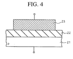
- Fig. 4 is the cross-sectional view showing the sample for investigation.
- reference numeral 21 denotes the Si substrate as the substrate subject to deposition
- 22 the insulating film formed by the deposition method of the present invention
- 23 the electrode.
- Fig. 3 is the view showing the relationship between a electric field intensity and the leakage current of the insulating film 22 when a voltage is applied between the substrate 21 and the electrode 23.
- the axis of ordinate shows the leakage current value (A) of the insulating film 22, which is expressed in the linear scale, and the axis of abscissas shows the electric field intensity (MV/cm) expressed in the linear scale.
- the leakage current is in the 10 -10 A range at the electric field intensity of 1 MV/cm, and it is 10 -6 A at the electric field intensity of 5 MV/cm, where a sufficiently small leakage current was obtained.
- the film deposited is dense and diffusion preventing capability against copper is high.
- the insulating film is most suitable for using as the barrier insulating film that coats the copper wiring, making use of its characteristics of relatively low relative dielectric constant and high diffusion preventing capability.
- Figs. 5A to 5D are the cross-sectional views showing the manufacturing method of the semiconductor device according to the second embodiment of the present invention.
- TEOS+N 2 O+NH 3 are used as the film forming gas.
- a substrate 31 having a front-end insulating film formed on a surface thereof is prepared as shown in Fig. 5A.
- a lower wiring buried insulating film 32 formed of an SiO 2 film with the film thickness of about 1 ⁇ m having low relative dielectric constant from 2 to the 3 range is formed on the substrate 31 by a well-known method.
- a TaN film 34a as a copper diffusion preventing film is formed on an inner surface of a wiring groove 33 after the lower wiring buried insulating film 32 is etched to form the wiring groove 33. Then, after forming a copper seed layer (not shown) on the surface of the TaN film 34a by a sputtering method, a copper film is buried thereon by a plating method.
- the copper film and the TaN film 34a protruded from the wiring groove 33 are polished by a CMP method (Chemical Mechanical Polishing method) to make the surface flat.
- a CMP method Chemical Mechanical Polishing method
- the ones described above constitute the substrate subject to deposition 21.
- a barrier insulating film 35a formed of a PE-CVD SiO 2 film having the film thickness of about a few tens nm is formed by the plasma enhanced CVD method using TEOS+N 2 O+NH 3 on the lower wiring buried insulating film 32 while coating the copper wiring 34b that is exposed from the lower wiring buried insulating film 32.
- a main insulating film 35 formed of the PE-CVD SiO 2 film having low relative dielectric constant from 2 to the 3 range is formed on the barrier insulating film 35a by a well-known method.
- the barrier insulating film 35a and the main insulating film 35b constitute the inter wiring layer insulating film 35.
- the substrate subject to deposition 21 is introduced into a chamber 1 of the deposition apparatus 101 to be held by a substrate holder 3. Then, the substrate subject to deposition 21 is heated and its temperature is kept at 375°C.
- TEOS, N 2 O gas and NH 3 are introduced at the flow rate of 50 sccm, 50 sccm and 200 sccm respectively into the chamber 1 of the plasma enhanced deposition apparatus 101 shown in Fig. 1, and the pressure is kept at about 1.0 Torr.
- the low frequency electric power of about 150 W (electric power density: about 0.18 W/cm 2 ) having the frequency of 380 kHz is applied to the lower electrode 3.
- the high frequency electric power (frequency: 13.56 MHz) is not applied to the upper electrode 2.
- TEOS, N 2 O and NH 3 are thus transformed into plasma. This status is maintained for thirty seconds to form the barrier insulating film 35a formed of the PE-CVD SiO 2 film having the film thickness of about 10 to 50nm.
- the inter wiring layer insulating film 35 that consists of the barrier insulating film 35a and the main insulating film 35b is formed.
- an upper wiring buried insulating film 36 formed of the SiO 2 film having the film thickness of about 500nm is formed on the inter wiring layer insulating film 35 by the same method used in forming the lower wiring buried insulating film 32.
- connection conductor 37 and an upper wiring 38 which is mainly formed of a copper film, are formed by a well-known dual-damascene method.
- reference numerals 37a and 38a in the drawing denote the TaN film
- 37b and 38b denote the copper film.
- a barrier insulating film 39 formed of the PE-CVD SiO 2 is formed on the entire surface using the same deposition method as the one used in forming the barrier insulating film 35a. Thus, the semiconductor device is completed.
- the plasma enhanced CVD method using TEOS+N 2 O+NH 3 forms the barrier insulating film 35a that coats the copper film 34b, which constitutes the lower wiring 34.
- the barrier insulating film 35a having the relative dielectric constant in the 4 range which is low comparing to the relative dielectric constant of about 7 of the silicon nitride film, and high diffusion preventing capability against copper can be obtained.
- the inter wiring layer insulating film including the barrier insulating film 35a a multi-layer copper wiring can be formed while restricting excessive increase of parasitic capacitance and maintaining the diffusion preventing capability against copper.
- the semiconductor integrated circuit device that can deal with higher data transfer speed along with higher integration can be provided.
- hydrocarbon is not contained in the film forming gas in the second embodiment.
- hydrocarbon which is any one of methane (CH 4 ), acetylene (C 2 H 2 ), ethylene (C 2 H 4 ), and ethane (C 2 H 6 ) for example can be contained in the film forming gas as described in the first embodiment.
- hydrocarbon (C m H n ): any one of methane (CH 4 ), acetylene (C 2 H 2 ), ethylene (C 2 H 4 ), and ethane (C 2 H 6 ) is added to the film forming gas other than tetraethoxysilane and nitrogen monoxide, or tetraethoxysilane, nitrogen monoxide and ammonia (NH 3 ).
- inert gas containing any one of helium (He), argon (Ar) and nitrogen (N 2 ) may be contained in the film forming gas.
- the film forming gas containing tetraethoxysilane (TEOS) and nitrogen monoxide (N 2 O) is transformed into plasma to cause reaction, and the barrier insulating film is thus formed on the substrate subject to deposition. Accordingly, the barrier insulating film having diffusion preventing capability against copper while maintaining the relatively low relative dielectric constant in the 4 range can be formed.
- TEOS tetraethoxysilane
- N 2 O nitrogen monoxide
- ammonia (NH 3 ) added to the film forming gas of the barrier insulating film can improve the diffusion preventing capability against copper.
- hydrocarbon any one of methane (CH 4 ), acetylene (C 2 H 2 ), ethylene (C 2 H 4 ), and ethane (C 2 H 6 ) for example, other than tetraethoxysilane and nitrogen monoxide, or tetraethoxysilane, nitrogen monoxide and ammonia (NH 3 ) to the film forming gas of the barrier insulating film, the barrier insulating film with higher diffusion preventing capability against copper can be obtained while maintaining low relative dielectric constant.
- hydrocarbon C m H n
- the multi-layer copper wirings can be formed while restricting excessive increase of parasitic capacitance and maintaining the diffusion preventing capability against copper.
- the semiconductor integrated circuit device that can deal with higher data transfer speed along with higher integration and density can be thus provided.
Abstract


Description
- The present invention relates to a manufacturing method of a semiconductor device in which a barrier insulating film that coats a wiring, particularly a copper wiring is formed.
- In recent years, a higher data transfer speed has been required with higher integration of a semiconductor integrated circuit device. For this reason, a copper wiring is used. In this case, there is a need for an insulating film (hereinafter, referred to as a barrier insulating film) that has a function to prevent diffusion of copper from the copper wiring and a function as an etching stopper when a damascene method is applied, and that preferably has low relative dielectric constant.
- To form such a barrier insulating film, there is known a plasma enhanced CVD (Chemical Vapor Deposition) method using mixed gas composed of tetramethylsilane (Si(CH3)4), or other types of organic silane, and methane (CH4).
- Alternatively, there is known a silicon nitride film (hereinafter, referred to as an SiN film) deposited by the plasma enhanced CVD method as the barrier insulating film.
- However, there exists a problem that the barrier insulating film deposited using tetramethylsilane, or other types of organic silane, and methane has a large content of carbon and a large leakage current. There also exists a problem that the barrier insulating film as the silicon nitride film has relative dielectric constant of about 7 although it has a small leakage current.
- The object of the present invention is to provide a manufacturing method of a semiconductor device in which a barrier insulating film having low relative dielectric constant of 5 or less and a leakage current characteristic equal to that of a silicon nitride film is deposited.
- In this invention, film forming gas that contains tetraethoxysilane (TEOS) and nitrogen monoxide (N2O) is transformed into plasma to cause reaction to form the barrier insulating film on a substrate.
- Experiments resulted in a barrier insulating film having the relative dielectric constant in the 4 range, which is relatively low comparing to the relative dielectric constant of about 7 of the silicon nitride film, and having a small leakage current level equal to that of the silicon nitride film.
- Moreover, containing ammonia (NH3) in the film forming gas of the barrier insulating film results in improving barrier characteristic against copper of the barrier insulating film deposited, and the leakage current can be further reduced.
- Furthermore, when hydrocarbon (CmHn): any one of methane (CH4), acetylene (C2H2), ethylene (C2H4), and ethane (C2H6) for example is added to the film forming gas of the barrier insulating film other than tetraethoxysilane and nitrogen monoxide, or other than tetraethoxysilane, nitrogen monoxide and ammonia (NH3), a denser barrier insulating film having diffusion preventing capability against copper can be obtained while maintaining low relative dielectric constant.
-
- Fig. 1 is a side view showing a configuration of a plasma-enhanced deposition apparatus used in the manufacturing method of the semiconductor device, which is an embodiment of the present invention.
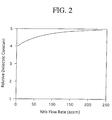
- Fig. 2 is a graph showing a relationship between relative dielectric constant of an insulating film deposited and an ammonia flow rate in a deposition method being a first embodiment of the present invention.
- Fig. 3 is a graph showing a leakage current of the insulating film deposited by the deposition method being the first embodiment of the present invention.
- Fig. 4 is a cross-sectional view showing a sample by which characteristics of the insulating film deposited by the deposition method, which is the first embodiment of the present invention, is inspected.
- Figs. 5A to 5D are cross-sectional views showing the semiconductor device and its manufacturing method, which are a second embodiment of the present invention.
-
- Embodiments of the present invention will be described as follows with reference to the drawings.
- Fig. 1 is the side view showing the configuration of a parallel plate type plasma enhanced
CVD apparatus 101 used in the manufacturing method of the semiconductor device according to the embodiment of the present invention. - The plasma enhanced
CVD apparatus 101 is provided with: adeposition section 101A that is a position where the insulating film is formed on a substrate subject todeposition 21 by plasma gas; and a film forminggas supply section 101B having a plurality of supply sources of gases that constitute the film forming gas. - The
deposition section 101A includes adecompressive chamber 1 as shown in Fig. 1, and thechamber 1 is connected with anexhaust unit 6 via anexhaust piping 4. Aswitching valve 5 that controls connection/disconnection between thechamber 1 and theexhaust unit 6 is provided halfway theexhaust piping 4. Thechamber 1 is provided with pressure measurement means such as a vacuum gauge (not shown) for monitoring a pressure inside thechamber 1. - There is provided in the chamber 1 a pair of an upper electrode (first electrode) 2 and a lower electrode (second electrode) 3, which oppose with each other. A high frequency electric power supply source (RF power source) 7 that supplies high frequency electric power having the frequency of 1 MHz or more, that is, generally 13.56 MHz is connected to the
upper electrode 2, and a low frequency electricpower supply source 8 that supplies low frequency electric power having the frequency of 100 kHz or more and less than 1 MHz, that is, generally 380 kHz is connected to thelower electrode 3. These power sources (7, 8) supply electric power to theupper electrode 2 and thelower electrode 3 respectively to transform the film forming gas into plasma. Theupper electrode 2, thelower electrode 3 and the power sources (7, 8) constitute plasma generation means that transforms the film forming gas into plasma. - The
upper electrode 2 also serves as a dispersion unit of the film forming gas. A plurality of through holes are formed on theupper electrode 2, and openings on the opposing side of the through holes to thelower electrode 3 are discharge ports (introduction ports) of the film forming gas. The discharge ports for the film forming gas or the like are connected with the film forminggas supply section 101B by apiping 9a. Further, there are cases where a heater (not shown) is provided for theupper electrode 2. This is because heating theupper electrode 2 to about 100°C during deposition prevents particles made of vapor-phase reaction product such as the film forming gas from adhering to theupper electrode 2. - The
lower electrode 3 also functions as a substrate holder for the substrate subject todeposition 21, and it includes aheater 12 that heats the substrate subject todeposition 21 on the substrate holder. - The film forming
gas supply section 101B are provided with: a supply source of alkyl compound having siloxane bond; a supply source of tetraethoxysilane (also referred to as tetraethylorthosilicate) (TEOS: Si(OC2H5)4); a supply source of nitrogen monoxide (N2O); a supply source of ammonia (NH3); a supply source of hydrocarbon (CmHn); a supply source of dilute gas (Ar or He); and a supply source of nitrogen (N2). - These gases are appropriately supplied into the
chamber 1 of thedeposition section 101A through branch piping (9b to 9g) and thepiping 9a where all the branch pipings (9b to 9g) is connected. Flow rate adjustment means (11a to 11f) and switching means (10b to 10m) that control open/close of the branch pipings (9b to 9g) are installed halfway the branch pipings (9b to 9g), and switching means 10a that controls open/close of thepiping 9a is provided halfway thepiping 9a. - Furthermore, switching means (10n, 10p to 10r), which control connection/disconnection between the supply source of nitrogen (N2) gas and the branch piping 9g connected thereto and other branch pipings (9b to 9e), are installed in order to purge residual gas in the branch piping (9b to 9e) by flowing the nitrogen (N2) gas. Note that the nitrogen (N2) gas also purges residual gas in the
piping 9a and thechamber 1 other than the branch pipings (9b to 9e). - As described above, the
foregoing deposition apparatus 101 is provided with: the supply source of tetraethoxysilane; and the supply source of nitrogen monoxide, and further provided with: the plasma generation means (2, 3, 7 and 8) that transform the film forming gas into plasma. - With this configuration, an insulating film having relatively low relative dielectric constant and the leakage current level equal to that of the silicon nitride film was obtained as shown in the following embodiments. A small leakage current means high barrier characteristic against copper, which is useful as the characteristic of the barrier insulating film that coats the copper wiring.
- Moreover, the deposition apparatus further includes: the supply source of ammonia (NH3) other than the supply source of tetraethoxysilane and the supply source of nitrogen monoxide. Adding ammonia (NH3) results in further improving the barrier characteristic against copper.
- The deposition apparatus further includes the supply source of hydrocarbon (CmHn), which is any one of methane (CH4), acetylene (C2H2), ethylene (C2H4), and ethane (C2H6) for example other than the supply source of tetraethoxysilane and the supply source of nitrogen monoxide, or other than the supply source of tetraethoxysilane, the supply source of nitrogen monoxide, and the supply source of ammonia (NH3). An even denser barrier insulating film having low relative dielectric constant can be obtained because the film deposited contains CH3 due to addition of hydrocarbon (CmHn).
- Then, there is provided means for generating plasma by the
upper electrode 2 and thelower electrode 3 of a parallel plate type, for example, as the plasma generation means, and the power sources (7, 8) for supplying electric power of two (high and low) frequencies are respectively connected to theupper electrode 2 and thelower electrode 3. Accordingly, the electric power of two (high and low) frequencies is applied to each electrode (2, 3), and thus plasma can be generated. Particularly, the barrier insulating film generated in this manner is dense and has lower relative dielectric constant. - Following is a method of applying the electric power to the
upper electrode 2 and thelower electrode 3. Specifically, the low frequency electric power having the frequency of 100 kHz or more and less than 1 MHz is applied only to thelower electrode 3, the low frequency electric power is applied to thelower electrode 3 and the high frequency electric power having the frequency of 1 MHz or more is applied to theupper electrode 2, or the high frequency electric power is applied only to theupper electrode 2. - Next, gas shown below may be used as a typical example of the hydrocarbon and the dilute gas corresponding to the film forming gas to which are applied for the present invention.
- (i) Hydrocarbon (CmHn)
methane (CH4)
acetylene (C2H2)
ethylene (C2H4)
ethane (C2H6) - (ii) Dilute gas
Helium (He)
Argon (Ar)
Nitrogen (N2) -
- Note that the foregoing gases can be variously combined to compose the film forming gas. For example, a film forming gas composed of tetraethoxysilane and nitrogen monoxide, which does not contain ammonia (NH3), may be used. Alternatively, a film forming gas composed of tetraethoxysilane, nitrogen monoxide and ammonia (NH3) may also be used.
- In addition, hydrocarbon or dilute gas can be further added to the film forming gas of such combinations. In other words, hydrocarbon, that is, any one of methane (CH4), acetylene (C2H2), ethylene (C2H4) and ethane (C2H6) for example may be further added to the film forming gas of the foregoing combinations. In this case, even denser barrier insulating film can be obtained while maintaining the low relative dielectric constant in the 4 range.
- Still further, the foregoing dilute gas is added to the film forming gas, and thus the concentration of silicon-containing gas, ammonia or hydrocarbon can be adjusted.
- Next, description will be made for the experiment performed by the inventor.
- A silicon oxide film was deposited on an Si substrate by a plasma enhanced CVD method (PECVD method) under the following deposition conditions. Tetraethoxysilane (TEOS), nitrogen monoxide (N2O) and ammonia (NH3) were used as the film forming gas.
- An insulating film for investigation was deposited by changing the ammonia flow rate among the parameters of deposition conditions in the range of 0 to 250 sccm.
- The deposition conditions including the ammonia flow rate are as follows. Note that one minute and thirty seconds are reserved for time (stabilization period) necessary for substituting gas inside the chamber from gas introduction to start of deposition (plasma excitation) during deposition, and the
upper electrode 2 is heated to 100°C to prevent the reaction product from adhering to theupper electrode 2. -
- (i)Film forming gas
TEOS flow rate: 50 sccm
N2O flow rate: 50 sccm
NH3 flow rate (parameter): 0 to 250 sccm Gas pressure: approximately 1.0 Torr - (ii)Plasma excitation conditions
Lower electrode
Low frequency electric power (frequency: 380 kHz): 150 W
Upper electrode
High frequency electric power (frequency: 13.56 MHz): 0 W - (iii)Substrate heating conditions: 375°C
-
- Fig. 4 is the cross-sectional view showing the sample for investigation. In the drawing,
reference numeral 21 denotes the Si substrate as the substrate subject to deposition, 22: the insulating film formed by the deposition method of the present invention, and 23: the electrode. - (a) Relative Dielectric constant of film deposited Investigation was made for the dielectric constant of the insulating film deposited under the foregoing deposition conditions and by changing the ammonia flow rate in the range of 0 to 250 sccm. The film shown in Fig. 4 was used as the sample for investigation.Fig. 2 is the graph showing the relationship between the relative dielectric constant of the insulating film deposited and the ammonia flow rate. The axis of ordinate shows the relative dielectric constant of the film deposited, which is expressed in a linear scale, and the axis of abscissas shows the ammonia flow rate (sccm) expressed in the linear scale.The relative dielectric constant was measured by a C-V measurement method, in which a signal having a frequency of 1 MHz is superposed to direct current bias.According to Fig. 2, the relative dielectric constant is about 4 at the ammonia flow rate of 0, it gradually increases as the ammonia flow rate increases and changes so as to gradually approximate to the relative dielectric constant of 5. Specifically, the relative dielectric constant in the 4 range can be at least obtained at the ammonia flow rate of 250 sccm or less.
- (b) Leakage current of film deposited Investigation was made for the leakage current of the insulating film deposited under the foregoing deposition conditions and at the ammonia flow rate of 200 sccm. The film shown in Fig. 4 was used as the sample for investigation. The leakage current value relates to the density of the film deposited, by which the barrier characteristic against copper can be estimated.
-
- Fig. 3 is the view showing the relationship between a electric field intensity and the leakage current of the insulating
film 22 when a voltage is applied between thesubstrate 21 and theelectrode 23. The axis of ordinate shows the leakage current value (A) of the insulatingfilm 22, which is expressed in the linear scale, and the axis of abscissas shows the electric field intensity (MV/cm) expressed in the linear scale. - According to Fig. 3, the leakage current is in the 10-10 A range at the electric field intensity of 1 MV/cm, and it is 10-6 A at the electric field intensity of 5 MV/cm, where a sufficiently small leakage current was obtained. This shows that the film deposited is dense and diffusion preventing capability against copper is high.
- As described, according to the first embodiment, the dense insulating film having the relative dielectric constant of 5 or less and in the 4 range, which is low comparing to the relative dielectric constant of about 7 of the silicon nitride film, was obtained.
- Although the relative dielectric constant needs to be further reduced in order to use the insulating film as a main inter layer dielectric between the copper wirings, for example, the insulating film is most suitable for using as the barrier insulating film that coats the copper wiring, making use of its characteristics of relatively low relative dielectric constant and high diffusion preventing capability.
- Description will be made for the semiconductor device and manufacturing method thereof according to the second embodiment of the present invention with reference to Figs. 5A to 5D.
- Figs. 5A to 5D are the cross-sectional views showing the manufacturing method of the semiconductor device according to the second embodiment of the present invention. TEOS+N2O+NH3 are used as the film forming gas.
- Firstly, a
substrate 31 having a front-end insulating film formed on a surface thereof is prepared as shown in Fig. 5A. A lower wiring buried insulatingfilm 32 formed of an SiO2 film with the film thickness of about 1µm having low relative dielectric constant from 2 to the 3 range is formed on thesubstrate 31 by a well-known method. - Subsequently, as shown in Fig. 5A, a TaN film 34a as a copper diffusion preventing film is formed on an inner surface of a
wiring groove 33 after the lower wiring buried insulatingfilm 32 is etched to form thewiring groove 33. Then, after forming a copper seed layer (not shown) on the surface of the TaN film 34a by a sputtering method, a copper film is buried thereon by a plating method. - Thereafter, the copper film and the TaN film 34a protruded from the
wiring groove 33 are polished by a CMP method (Chemical Mechanical Polishing method) to make the surface flat. Thus, a lower wiring 34 formed of thecopper wiring 34b and the TaN film 34a is formed. - The ones described above constitute the substrate subject to
deposition 21. - Next, as shown in Fig. 5B, a
barrier insulating film 35a formed of a PE-CVD SiO2 film having the film thickness of about a few tens nm is formed by the plasma enhanced CVD method using TEOS+N2O+NH3 on the lower wiring buried insulatingfilm 32 while coating thecopper wiring 34b that is exposed from the lower wiring buried insulatingfilm 32. - Subsequently, as shown in Fig. 5C, a main insulating
film 35 formed of the PE-CVD SiO2 film having low relative dielectric constant from 2 to the 3 range is formed on thebarrier insulating film 35a by a well-known method. Thebarrier insulating film 35a and the main insulatingfilm 35b constitute the inter wiringlayer insulating film 35. - Details of the deposition method of the inter wiring
layer insulating film 35 will be described as follows. - Specifically, to form the inter wiring
layer insulating film 35, the substrate subject todeposition 21 is introduced into achamber 1 of thedeposition apparatus 101 to be held by asubstrate holder 3. Then, the substrate subject todeposition 21 is heated and its temperature is kept at 375°C. - Next, TEOS, N2O gas and NH3 are introduced at the flow rate of 50 sccm, 50 sccm and 200 sccm respectively into the
chamber 1 of the plasma enhanceddeposition apparatus 101 shown in Fig. 1, and the pressure is kept at about 1.0 Torr. - Then, the low frequency electric power of about 150 W (electric power density: about 0.18 W/cm2) having the frequency of 380 kHz is applied to the
lower electrode 3. At this point, the high frequency electric power (frequency: 13.56 MHz) is not applied to theupper electrode 2. - TEOS, N2O and NH3 are thus transformed into plasma. This status is maintained for thirty seconds to form the
barrier insulating film 35a formed of the PE-CVD SiO2 film having the film thickness of about 10 to 50nm. - A porous
insulating film 35b having the film thickness of about 500nm, which is the main insulating film, is subsequently formed on thebarrier insulating film 35a. - As described above, the inter wiring
layer insulating film 35 that consists of thebarrier insulating film 35a and the main insulatingfilm 35b is formed. - Next, as shown in Fig. 5D, an upper wiring buried insulating
film 36 formed of the SiO2 film having the film thickness of about 500nm is formed on the inter wiringlayer insulating film 35 by the same method used in forming the lower wiring buried insulatingfilm 32. - Then, a
connection conductor 37 and anupper wiring 38, which is mainly formed of a copper film, are formed by a well-known dual-damascene method. Note thatreference numerals - Next, a
barrier insulating film 39 formed of the PE-CVD SiO2 is formed on the entire surface using the same deposition method as the one used in forming thebarrier insulating film 35a. Thus, the semiconductor device is completed. - As described above, according to the second embodiment, in the manufacturing method of the semiconductor device in which the inter wiring
layer insulating film 35 is sandwiched between the lower wiring buried insulatingfilm 32, in which the lower wiring 34 is buried, and the upper wiring buried insulatingfilm 36, in which theupper wiring 38 is buried, the plasma enhanced CVD method using TEOS+N2O+NH3 forms thebarrier insulating film 35a that coats thecopper film 34b, which constitutes the lower wiring 34. - Therefore, the
barrier insulating film 35a having the relative dielectric constant in the 4 range, which is low comparing to the relative dielectric constant of about 7 of the silicon nitride film, and high diffusion preventing capability against copper can be obtained. Thus, with intervention of the inter wiring layer insulating film including thebarrier insulating film 35a, a multi-layer copper wiring can be formed while restricting excessive increase of parasitic capacitance and maintaining the diffusion preventing capability against copper. - With this configuration, the semiconductor integrated circuit device that can deal with higher data transfer speed along with higher integration can be provided.
- As in the foregoing, although the present invention has been described in detail based on the embodiments, the scope of the present invention is not limited to the examples specifically shown in the embodiments. Changes of the foregoing embodiments within the scope of the spirit of the present invention are included in the scope of the present invention.
- For example, hydrocarbon is not contained in the film forming gas in the second embodiment. However, hydrocarbon, which is any one of methane (CH4), acetylene (C2H2), ethylene (C2H4), and ethane (C2H6) for example can be contained in the film forming gas as described in the first embodiment. In this case, hydrocarbon (CmHn): any one of methane (CH4), acetylene (C2H2), ethylene (C2H4), and ethane (C2H6) is added to the film forming gas other than tetraethoxysilane and nitrogen monoxide, or tetraethoxysilane, nitrogen monoxide and ammonia (NH3).
- Alternatively, inert gas containing any one of helium (He), argon (Ar) and nitrogen (N2) may be contained in the film forming gas.
- In the present invention, the film forming gas containing tetraethoxysilane (TEOS) and nitrogen monoxide (N2O) is transformed into plasma to cause reaction, and the barrier insulating film is thus formed on the substrate subject to deposition. Accordingly, the barrier insulating film having diffusion preventing capability against copper while maintaining the relatively low relative dielectric constant in the 4 range can be formed.
- Moreover, addition of ammonia (NH3) to the film forming gas of the barrier insulating film can improve the diffusion preventing capability against copper.
- Furthermore, with addition of hydrocarbon (CmHn): any one of methane (CH4), acetylene (C2H2), ethylene (C2H4), and ethane (C2H6) for example, other than tetraethoxysilane and nitrogen monoxide, or tetraethoxysilane, nitrogen monoxide and ammonia (NH3) to the film forming gas of the barrier insulating film, the barrier insulating film with higher diffusion preventing capability against copper can be obtained while maintaining low relative dielectric constant.
- Accordingly, with intervention of the inter wiring layer insulating film including the barrier insulating film, the multi-layer copper wirings can be formed while restricting excessive increase of parasitic capacitance and maintaining the diffusion preventing capability against copper. The semiconductor integrated circuit device that can deal with higher data transfer speed along with higher integration and density can be thus provided.
Claims (6)
- A manufacturing method of a semiconductor device, comprising the steps of:transforming film forming gas containing tetraethoxysilane (TEOS) and nitrogen monoxide (N2O) into plasma to cause reaction; andforming a barrier insulating film (35a, 39) that coats copper wiring (34, 38) on a substrate (31) where said copper wiring (34, 38) is exposed on a surface thereof.
- The manufacturing method of a semiconductor device according to claim 1, wherein
said film forming gas further contains at least one of ammonia (NH3) and nitrogen (N2) other than tetraethoxysilane (TEOS) and nitrogen monoxide (N2O). - The manufacturing method of a semiconductor device according to claim 1, wherein
said film forming gas further contains hydrocarbon (CmHn) other than tetraethoxysilane (TEOS) and nitrogen monoxide (N2O). - The manufacturing method of a semiconductor device according to claim 3, wherein
said hydrocarbon (CmHn) is any one of methane (CH4), acetylene (C2H2), ethylene (C2H4), and ethane (C2H6). - The manufacturing method of a semiconductor device according to claim 2, wherein
said film forming gas further contains hydrocarbon (CmHn) other than tetraethoxysilane (TEOS), nitrogen monoxide (N2O), and at least any one of ammonia (NH3) and nitrogen (N2). - The manufacturing method of a semiconductor device according to claim 5, wherein
said hydrocarbon (CmHn) is any one of methane (CH4), acetylene (C2H2), ethylene (C2H4), and ethane (C2H6).
Applications Claiming Priority (2)
| Application Number | Priority Date | Filing Date | Title |
|---|---|---|---|
| JP2001106689A JP2002305242A (en) | 2001-04-05 | 2001-04-05 | Method for manufacturing semiconductor device |
| JP2001106689 | 2001-04-05 |
Publications (2)
| Publication Number | Publication Date |
|---|---|
| EP1247876A2 true EP1247876A2 (en) | 2002-10-09 |
| EP1247876A3 EP1247876A3 (en) | 2003-07-30 |
Family
ID=18959149
Family Applications (1)
| Application Number | Title | Priority Date | Filing Date |
|---|---|---|---|
| EP02007249A Withdrawn EP1247876A3 (en) | 2001-04-05 | 2002-03-28 | Method for manufacturing a semiconductor device |
Country Status (5)
| Country | Link |
|---|---|
| US (1) | US20020151175A1 (en) |
| EP (1) | EP1247876A3 (en) |
| JP (1) | JP2002305242A (en) |
| KR (1) | KR20020079412A (en) |
| TW (1) | TWI300606B (en) |
Families Citing this family (5)
| Publication number | Priority date | Publication date | Assignee | Title |
|---|---|---|---|---|
| JP4403824B2 (en) * | 2003-05-26 | 2010-01-27 | 東京エレクトロン株式会社 | Method for forming silicon nitride film |
| CN1577832A (en) * | 2003-07-07 | 2005-02-09 | 松下电器产业株式会社 | Semiconductor device and method for fabricating the same |
| JP2005236141A (en) * | 2004-02-20 | 2005-09-02 | Oki Electric Ind Co Ltd | Semiconductor device and method for manufacturing the same |
| US20120064682A1 (en) | 2010-09-14 | 2012-03-15 | Jang Kyung-Tae | Methods of Manufacturing Three-Dimensional Semiconductor Memory Devices |
| CN105993059A (en) * | 2014-02-13 | 2016-10-05 | 埃伦贝格尔及珀恩斯根有限公司 | Thermal overcurrent circuit breaker |
Citations (5)
| Publication number | Priority date | Publication date | Assignee | Title |
|---|---|---|---|---|
| JPH04154125A (en) * | 1990-10-18 | 1992-05-27 | Nec Corp | Formation of silicon oxynitride film |
| US5869394A (en) * | 1996-10-29 | 1999-02-09 | Mosel Vitelic, Inc. | Teos-ozone planarization process |
| EP0935283A2 (en) * | 1998-02-05 | 1999-08-11 | Asm Japan K.K. | Silicone polymer insulation film on semiconductor substrate and method for forming the film |
| US6070550A (en) * | 1996-09-12 | 2000-06-06 | Applied Materials, Inc. | Apparatus for the stabilization of halogen-doped films through the use of multiple sealing layers |
| US6184158B1 (en) * | 1996-12-23 | 2001-02-06 | Lam Research Corporation | Inductively coupled plasma CVD |
Family Cites Families (6)
| Publication number | Priority date | Publication date | Assignee | Title |
|---|---|---|---|---|
| US5356722A (en) * | 1992-06-10 | 1994-10-18 | Applied Materials, Inc. | Method for depositing ozone/TEOS silicon oxide films of reduced surface sensitivity |
| US5612254A (en) * | 1992-06-29 | 1997-03-18 | Intel Corporation | Methods of forming an interconnect on a semiconductor substrate |
| US6294799B1 (en) * | 1995-11-27 | 2001-09-25 | Semiconductor Energy Laboratory Co., Ltd. | Semiconductor device and method of fabricating same |
| JP2975934B2 (en) * | 1997-09-26 | 1999-11-10 | 三洋電機株式会社 | Semiconductor device manufacturing method and semiconductor device |
| JP2000174123A (en) * | 1998-12-09 | 2000-06-23 | Nec Corp | Semiconductor device and manufacture thereof |
| US6541367B1 (en) * | 2000-01-18 | 2003-04-01 | Applied Materials, Inc. | Very low dielectric constant plasma-enhanced CVD films |
-
2001
- 2001-04-05 JP JP2001106689A patent/JP2002305242A/en active Pending
-
2002
- 2002-03-26 US US10/105,793 patent/US20020151175A1/en not_active Abandoned
- 2002-03-28 TW TW091106182A patent/TWI300606B/en not_active IP Right Cessation
- 2002-03-28 EP EP02007249A patent/EP1247876A3/en not_active Withdrawn
- 2002-04-02 KR KR1020020017959A patent/KR20020079412A/en not_active Application Discontinuation
Patent Citations (5)
| Publication number | Priority date | Publication date | Assignee | Title |
|---|---|---|---|---|
| JPH04154125A (en) * | 1990-10-18 | 1992-05-27 | Nec Corp | Formation of silicon oxynitride film |
| US6070550A (en) * | 1996-09-12 | 2000-06-06 | Applied Materials, Inc. | Apparatus for the stabilization of halogen-doped films through the use of multiple sealing layers |
| US5869394A (en) * | 1996-10-29 | 1999-02-09 | Mosel Vitelic, Inc. | Teos-ozone planarization process |
| US6184158B1 (en) * | 1996-12-23 | 2001-02-06 | Lam Research Corporation | Inductively coupled plasma CVD |
| EP0935283A2 (en) * | 1998-02-05 | 1999-08-11 | Asm Japan K.K. | Silicone polymer insulation film on semiconductor substrate and method for forming the film |
Non-Patent Citations (1)
| Title |
|---|
| PATENT ABSTRACTS OF JAPAN vol. 016, no. 441 (E-1264), 14 September 1992 (1992-09-14) & JP 04 154125 A (NEC CORP), 27 May 1992 (1992-05-27) * |
Also Published As
| Publication number | Publication date |
|---|---|
| EP1247876A3 (en) | 2003-07-30 |
| JP2002305242A (en) | 2002-10-18 |
| TWI300606B (en) | 2008-09-01 |
| US20020151175A1 (en) | 2002-10-17 |
| KR20020079412A (en) | 2002-10-19 |
Similar Documents
| Publication | Publication Date | Title |
|---|---|---|
| US6649495B2 (en) | Manufacturing method of semiconductor device | |
| US6479409B2 (en) | Fabrication of a semiconductor device with an interlayer insulating film formed from a plasma devoid of an oxidizing agent | |
| US6852651B2 (en) | Semiconductor device and method of manufacturing the same | |
| KR100484322B1 (en) | Semiconductor device and method of manufacturing the same | |
| US20050221622A1 (en) | Deposition method and semiconductor device | |
| KR20010106215A (en) | Semiconductor device and method of manufacturing the same | |
| KR100546958B1 (en) | Semiconductor device and method of manufacturing the same | |
| US6673725B2 (en) | Semiconductor device and method of manufacturing the same | |
| US20070237970A1 (en) | Diffusion barrier with low dielectric constant and semiconductor device containing same | |
| US6630412B2 (en) | Semiconductor device and method of manufacturing the same | |
| US6713383B2 (en) | Semiconductor device manufacturing method | |
| EP1321975A2 (en) | Method for plasma depositing an insulating film with low dielectric constant for a semiconductor device | |
| EP1247876A2 (en) | Method for manufacturing a semiconductor device | |
| EP1128421A2 (en) | Method of fabricating an interlayer insulating film comprising Si, O, C and H for semiconductor devices | |
| JP2004200713A (en) | Semiconductor device and method of manufacturing the same |
Legal Events
| Date | Code | Title | Description |
|---|---|---|---|
| PUAI | Public reference made under article 153(3) epc to a published international application that has entered the european phase |
Free format text: ORIGINAL CODE: 0009012 |
|
| AK | Designated contracting states |
Kind code of ref document: A2 Designated state(s): AT BE CH CY DE DK ES FI FR GB GR IE IT LI LU MC NL PT SE TR |
|
| AX | Request for extension of the european patent |
Free format text: AL;LT;LV;MK;RO;SI |
|
| PUAL | Search report despatched |
Free format text: ORIGINAL CODE: 0009013 |
|
| AK | Designated contracting states |
Designated state(s): AT BE CH CY DE DK ES FI FR GB GR IE IT LI LU MC NL PT SE TR |
|
| AX | Request for extension of the european patent |
Extension state: AL LT LV MK RO SI |
|
| RIC1 | Information provided on ipc code assigned before grant |
Ipc: 7H 01L 21/316 B Ipc: 7H 01L 21/768 B Ipc: 7H 01L 21/00 B Ipc: 7C 23C 16/40 A |
|
| 17P | Request for examination filed |
Effective date: 20031223 |
|
| AKX | Designation fees paid |
Designated state(s): DE FR GB NL |
|
| STAA | Information on the status of an ep patent application or granted ep patent |
Free format text: STATUS: THE APPLICATION IS DEEMED TO BE WITHDRAWN |
|
| 18D | Application deemed to be withdrawn |
Effective date: 20060725 |