EP1248295A2 - Semiconductor element, connection structure thereof, semiconductor device using a plurality of such elements and processes for making the same - Google Patents
Semiconductor element, connection structure thereof, semiconductor device using a plurality of such elements and processes for making the same Download PDFInfo
- Publication number
- EP1248295A2 EP1248295A2 EP20020007769 EP02007769A EP1248295A2 EP 1248295 A2 EP1248295 A2 EP 1248295A2 EP 20020007769 EP20020007769 EP 20020007769 EP 02007769 A EP02007769 A EP 02007769A EP 1248295 A2 EP1248295 A2 EP 1248295A2
- Authority
- EP
- European Patent Office
- Prior art keywords
- conductive bump
- semiconductor element
- semiconductor
- conductive
- bump
- Prior art date
- Legal status (The legal status is an assumption and is not a legal conclusion. Google has not performed a legal analysis and makes no representation as to the accuracy of the status listed.)
- Withdrawn
Links
- 239000004065 semiconductor Substances 0.000 title claims abstract description 139
- 238000000034 method Methods 0.000 title claims description 13
- 230000008569 process Effects 0.000 title claims description 11
- VYPSYNLAJGMNEJ-UHFFFAOYSA-N Silicium dioxide Chemical compound O=[Si]=O VYPSYNLAJGMNEJ-UHFFFAOYSA-N 0.000 claims abstract description 14
- 229910052681 coesite Inorganic materials 0.000 claims abstract description 7
- 229910052906 cristobalite Inorganic materials 0.000 claims abstract description 7
- 239000000377 silicon dioxide Substances 0.000 claims abstract description 7
- 229910052682 stishovite Inorganic materials 0.000 claims abstract description 7
- 229910052905 tridymite Inorganic materials 0.000 claims abstract description 7
- 229910052737 gold Inorganic materials 0.000 claims abstract description 6
- 229910052802 copper Inorganic materials 0.000 claims abstract description 4
- 239000000463 material Substances 0.000 claims description 8
- 230000000149 penetrating effect Effects 0.000 claims description 6
- 239000011248 coating agent Substances 0.000 claims description 4
- 238000000576 coating method Methods 0.000 claims description 4
- 238000004519 manufacturing process Methods 0.000 claims description 4
- 239000013039 cover film Substances 0.000 abstract description 11
- 238000009413 insulation Methods 0.000 abstract description 11
- 230000004044 response Effects 0.000 abstract description 4
- 239000010408 film Substances 0.000 description 8
- 229910000679 solder Inorganic materials 0.000 description 4
- 238000007747 plating Methods 0.000 description 2
- 229920005989 resin Polymers 0.000 description 2
- 239000011347 resin Substances 0.000 description 2
- BOTDANWDWHJENH-UHFFFAOYSA-N Tetraethyl orthosilicate Chemical compound CCO[Si](OCC)(OCC)OCC BOTDANWDWHJENH-UHFFFAOYSA-N 0.000 description 1
- 229910045601 alloy Inorganic materials 0.000 description 1
- 239000000956 alloy Substances 0.000 description 1
- 239000003822 epoxy resin Substances 0.000 description 1
- 239000012774 insulation material Substances 0.000 description 1
- 239000002184 metal Substances 0.000 description 1
- 229910052751 metal Inorganic materials 0.000 description 1
- 230000004048 modification Effects 0.000 description 1
- 238000012986 modification Methods 0.000 description 1
- 229920000647 polyepoxide Polymers 0.000 description 1
- 230000009467 reduction Effects 0.000 description 1
- 238000004544 sputter deposition Methods 0.000 description 1
Images


Classifications
-
- H—ELECTRICITY
- H01—ELECTRIC ELEMENTS
- H01L—SEMICONDUCTOR DEVICES NOT COVERED BY CLASS H10
- H01L21/00—Processes or apparatus adapted for the manufacture or treatment of semiconductor or solid state devices or of parts thereof
- H01L21/02—Manufacture or treatment of semiconductor devices or of parts thereof
- H01L21/04—Manufacture or treatment of semiconductor devices or of parts thereof the devices having at least one potential-jump barrier or surface barrier, e.g. PN junction, depletion layer or carrier concentration layer
- H01L21/50—Assembly of semiconductor devices using processes or apparatus not provided for in a single one of the subgroups H01L21/06 - H01L21/326, e.g. sealing of a cap to a base of a container
- H01L21/56—Encapsulations, e.g. encapsulation layers, coatings
- H01L21/563—Encapsulation of active face of flip-chip device, e.g. underfilling or underencapsulation of flip-chip, encapsulation preform on chip or mounting substrate
-
- H—ELECTRICITY
- H01—ELECTRIC ELEMENTS
- H01L—SEMICONDUCTOR DEVICES NOT COVERED BY CLASS H10
- H01L23/00—Details of semiconductor or other solid state devices
- H01L23/48—Arrangements for conducting electric current to or from the solid state body in operation, e.g. leads, terminal arrangements ; Selection of materials therefor
- H01L23/481—Internal lead connections, e.g. via connections, feedthrough structures
-
- H—ELECTRICITY
- H01—ELECTRIC ELEMENTS
- H01L—SEMICONDUCTOR DEVICES NOT COVERED BY CLASS H10
- H01L25/00—Assemblies consisting of a plurality of individual semiconductor or other solid state devices ; Multistep manufacturing processes thereof
- H01L25/03—Assemblies consisting of a plurality of individual semiconductor or other solid state devices ; Multistep manufacturing processes thereof all the devices being of a type provided for in the same subgroup of groups H01L27/00 - H01L33/00, or in a single subclass of H10K, H10N, e.g. assemblies of rectifier diodes
- H01L25/04—Assemblies consisting of a plurality of individual semiconductor or other solid state devices ; Multistep manufacturing processes thereof all the devices being of a type provided for in the same subgroup of groups H01L27/00 - H01L33/00, or in a single subclass of H10K, H10N, e.g. assemblies of rectifier diodes the devices not having separate containers
- H01L25/065—Assemblies consisting of a plurality of individual semiconductor or other solid state devices ; Multistep manufacturing processes thereof all the devices being of a type provided for in the same subgroup of groups H01L27/00 - H01L33/00, or in a single subclass of H10K, H10N, e.g. assemblies of rectifier diodes the devices not having separate containers the devices being of a type provided for in group H01L27/00
- H01L25/0657—Stacked arrangements of devices
-
- H—ELECTRICITY
- H01—ELECTRIC ELEMENTS
- H01L—SEMICONDUCTOR DEVICES NOT COVERED BY CLASS H10
- H01L2224/00—Indexing scheme for arrangements for connecting or disconnecting semiconductor or solid-state bodies and methods related thereto as covered by H01L24/00
- H01L2224/01—Means for bonding being attached to, or being formed on, the surface to be connected, e.g. chip-to-package, die-attach, "first-level" interconnects; Manufacturing methods related thereto
- H01L2224/02—Bonding areas; Manufacturing methods related thereto
- H01L2224/04—Structure, shape, material or disposition of the bonding areas prior to the connecting process
- H01L2224/05—Structure, shape, material or disposition of the bonding areas prior to the connecting process of an individual bonding area
- H01L2224/0554—External layer
- H01L2224/0556—Disposition
- H01L2224/05568—Disposition the whole external layer protruding from the surface
-
- H—ELECTRICITY
- H01—ELECTRIC ELEMENTS
- H01L—SEMICONDUCTOR DEVICES NOT COVERED BY CLASS H10
- H01L2224/00—Indexing scheme for arrangements for connecting or disconnecting semiconductor or solid-state bodies and methods related thereto as covered by H01L24/00
- H01L2224/01—Means for bonding being attached to, or being formed on, the surface to be connected, e.g. chip-to-package, die-attach, "first-level" interconnects; Manufacturing methods related thereto
- H01L2224/02—Bonding areas; Manufacturing methods related thereto
- H01L2224/04—Structure, shape, material or disposition of the bonding areas prior to the connecting process
- H01L2224/05—Structure, shape, material or disposition of the bonding areas prior to the connecting process of an individual bonding area
- H01L2224/0554—External layer
- H01L2224/05573—Single external layer
-
- H—ELECTRICITY
- H01—ELECTRIC ELEMENTS
- H01L—SEMICONDUCTOR DEVICES NOT COVERED BY CLASS H10
- H01L2224/00—Indexing scheme for arrangements for connecting or disconnecting semiconductor or solid-state bodies and methods related thereto as covered by H01L24/00
- H01L2224/01—Means for bonding being attached to, or being formed on, the surface to be connected, e.g. chip-to-package, die-attach, "first-level" interconnects; Manufacturing methods related thereto
- H01L2224/10—Bump connectors; Manufacturing methods related thereto
- H01L2224/15—Structure, shape, material or disposition of the bump connectors after the connecting process
- H01L2224/16—Structure, shape, material or disposition of the bump connectors after the connecting process of an individual bump connector
- H01L2224/161—Disposition
- H01L2224/16135—Disposition the bump connector connecting between different semiconductor or solid-state bodies, i.e. chip-to-chip
- H01L2224/16145—Disposition the bump connector connecting between different semiconductor or solid-state bodies, i.e. chip-to-chip the bodies being stacked
-
- H—ELECTRICITY
- H01—ELECTRIC ELEMENTS
- H01L—SEMICONDUCTOR DEVICES NOT COVERED BY CLASS H10
- H01L2224/00—Indexing scheme for arrangements for connecting or disconnecting semiconductor or solid-state bodies and methods related thereto as covered by H01L24/00
- H01L2224/01—Means for bonding being attached to, or being formed on, the surface to be connected, e.g. chip-to-package, die-attach, "first-level" interconnects; Manufacturing methods related thereto
- H01L2224/10—Bump connectors; Manufacturing methods related thereto
- H01L2224/15—Structure, shape, material or disposition of the bump connectors after the connecting process
- H01L2224/16—Structure, shape, material or disposition of the bump connectors after the connecting process of an individual bump connector
- H01L2224/161—Disposition
- H01L2224/16151—Disposition the bump connector connecting between a semiconductor or solid-state body and an item not being a semiconductor or solid-state body, e.g. chip-to-substrate, chip-to-passive
- H01L2224/16221—Disposition the bump connector connecting between a semiconductor or solid-state body and an item not being a semiconductor or solid-state body, e.g. chip-to-substrate, chip-to-passive the body and the item being stacked
- H01L2224/16225—Disposition the bump connector connecting between a semiconductor or solid-state body and an item not being a semiconductor or solid-state body, e.g. chip-to-substrate, chip-to-passive the body and the item being stacked the item being non-metallic, e.g. insulating substrate with or without metallisation
-
- H—ELECTRICITY
- H01—ELECTRIC ELEMENTS
- H01L—SEMICONDUCTOR DEVICES NOT COVERED BY CLASS H10
- H01L2224/00—Indexing scheme for arrangements for connecting or disconnecting semiconductor or solid-state bodies and methods related thereto as covered by H01L24/00
- H01L2224/01—Means for bonding being attached to, or being formed on, the surface to be connected, e.g. chip-to-package, die-attach, "first-level" interconnects; Manufacturing methods related thereto
- H01L2224/26—Layer connectors, e.g. plate connectors, solder or adhesive layers; Manufacturing methods related thereto
- H01L2224/31—Structure, shape, material or disposition of the layer connectors after the connecting process
- H01L2224/32—Structure, shape, material or disposition of the layer connectors after the connecting process of an individual layer connector
- H01L2224/321—Disposition
- H01L2224/32135—Disposition the layer connector connecting between different semiconductor or solid-state bodies, i.e. chip-to-chip
- H01L2224/32145—Disposition the layer connector connecting between different semiconductor or solid-state bodies, i.e. chip-to-chip the bodies being stacked
-
- H—ELECTRICITY
- H01—ELECTRIC ELEMENTS
- H01L—SEMICONDUCTOR DEVICES NOT COVERED BY CLASS H10
- H01L2224/00—Indexing scheme for arrangements for connecting or disconnecting semiconductor or solid-state bodies and methods related thereto as covered by H01L24/00
- H01L2224/01—Means for bonding being attached to, or being formed on, the surface to be connected, e.g. chip-to-package, die-attach, "first-level" interconnects; Manufacturing methods related thereto
- H01L2224/26—Layer connectors, e.g. plate connectors, solder or adhesive layers; Manufacturing methods related thereto
- H01L2224/31—Structure, shape, material or disposition of the layer connectors after the connecting process
- H01L2224/32—Structure, shape, material or disposition of the layer connectors after the connecting process of an individual layer connector
- H01L2224/321—Disposition
- H01L2224/32151—Disposition the layer connector connecting between a semiconductor or solid-state body and an item not being a semiconductor or solid-state body, e.g. chip-to-substrate, chip-to-passive
- H01L2224/32221—Disposition the layer connector connecting between a semiconductor or solid-state body and an item not being a semiconductor or solid-state body, e.g. chip-to-substrate, chip-to-passive the body and the item being stacked
- H01L2224/32225—Disposition the layer connector connecting between a semiconductor or solid-state body and an item not being a semiconductor or solid-state body, e.g. chip-to-substrate, chip-to-passive the body and the item being stacked the item being non-metallic, e.g. insulating substrate with or without metallisation
-
- H—ELECTRICITY
- H01—ELECTRIC ELEMENTS
- H01L—SEMICONDUCTOR DEVICES NOT COVERED BY CLASS H10
- H01L2224/00—Indexing scheme for arrangements for connecting or disconnecting semiconductor or solid-state bodies and methods related thereto as covered by H01L24/00
- H01L2224/73—Means for bonding being of different types provided for in two or more of groups H01L2224/10, H01L2224/18, H01L2224/26, H01L2224/34, H01L2224/42, H01L2224/50, H01L2224/63, H01L2224/71
- H01L2224/732—Location after the connecting process
- H01L2224/73201—Location after the connecting process on the same surface
- H01L2224/73203—Bump and layer connectors
- H01L2224/73204—Bump and layer connectors the bump connector being embedded into the layer connector
-
- H—ELECTRICITY
- H01—ELECTRIC ELEMENTS
- H01L—SEMICONDUCTOR DEVICES NOT COVERED BY CLASS H10
- H01L2225/00—Details relating to assemblies covered by the group H01L25/00 but not provided for in its subgroups
- H01L2225/03—All the devices being of a type provided for in the same subgroup of groups H01L27/00 - H01L33/648 and H10K99/00
- H01L2225/04—All the devices being of a type provided for in the same subgroup of groups H01L27/00 - H01L33/648 and H10K99/00 the devices not having separate containers
- H01L2225/065—All the devices being of a type provided for in the same subgroup of groups H01L27/00 - H01L33/648 and H10K99/00 the devices not having separate containers the devices being of a type provided for in group H01L27/00
- H01L2225/06503—Stacked arrangements of devices
- H01L2225/06513—Bump or bump-like direct electrical connections between devices, e.g. flip-chip connection, solder bumps
-
- H—ELECTRICITY
- H01—ELECTRIC ELEMENTS
- H01L—SEMICONDUCTOR DEVICES NOT COVERED BY CLASS H10
- H01L2225/00—Details relating to assemblies covered by the group H01L25/00 but not provided for in its subgroups
- H01L2225/03—All the devices being of a type provided for in the same subgroup of groups H01L27/00 - H01L33/648 and H10K99/00
- H01L2225/04—All the devices being of a type provided for in the same subgroup of groups H01L27/00 - H01L33/648 and H10K99/00 the devices not having separate containers
- H01L2225/065—All the devices being of a type provided for in the same subgroup of groups H01L27/00 - H01L33/648 and H10K99/00 the devices not having separate containers the devices being of a type provided for in group H01L27/00
- H01L2225/06503—Stacked arrangements of devices
- H01L2225/06541—Conductive via connections through the device, e.g. vertical interconnects, through silicon via [TSV]
-
- H—ELECTRICITY
- H01—ELECTRIC ELEMENTS
- H01L—SEMICONDUCTOR DEVICES NOT COVERED BY CLASS H10
- H01L24/00—Arrangements for connecting or disconnecting semiconductor or solid-state bodies; Methods or apparatus related thereto
- H01L24/01—Means for bonding being attached to, or being formed on, the surface to be connected, e.g. chip-to-package, die-attach, "first-level" interconnects; Manufacturing methods related thereto
- H01L24/10—Bump connectors ; Manufacturing methods related thereto
- H01L24/12—Structure, shape, material or disposition of the bump connectors prior to the connecting process
- H01L24/13—Structure, shape, material or disposition of the bump connectors prior to the connecting process of an individual bump connector
-
- H—ELECTRICITY
- H01—ELECTRIC ELEMENTS
- H01L—SEMICONDUCTOR DEVICES NOT COVERED BY CLASS H10
- H01L24/00—Arrangements for connecting or disconnecting semiconductor or solid-state bodies; Methods or apparatus related thereto
- H01L24/01—Means for bonding being attached to, or being formed on, the surface to be connected, e.g. chip-to-package, die-attach, "first-level" interconnects; Manufacturing methods related thereto
- H01L24/10—Bump connectors ; Manufacturing methods related thereto
- H01L24/15—Structure, shape, material or disposition of the bump connectors after the connecting process
- H01L24/16—Structure, shape, material or disposition of the bump connectors after the connecting process of an individual bump connector
-
- H—ELECTRICITY
- H01—ELECTRIC ELEMENTS
- H01L—SEMICONDUCTOR DEVICES NOT COVERED BY CLASS H10
- H01L2924/00—Indexing scheme for arrangements or methods for connecting or disconnecting semiconductor or solid-state bodies as covered by H01L24/00
- H01L2924/01—Chemical elements
- H01L2924/01078—Platinum [Pt]
-
- H—ELECTRICITY
- H01—ELECTRIC ELEMENTS
- H01L—SEMICONDUCTOR DEVICES NOT COVERED BY CLASS H10
- H01L2924/00—Indexing scheme for arrangements or methods for connecting or disconnecting semiconductor or solid-state bodies as covered by H01L24/00
- H01L2924/01—Chemical elements
- H01L2924/01079—Gold [Au]
-
- H—ELECTRICITY
- H01—ELECTRIC ELEMENTS
- H01L—SEMICONDUCTOR DEVICES NOT COVERED BY CLASS H10
- H01L2924/00—Indexing scheme for arrangements or methods for connecting or disconnecting semiconductor or solid-state bodies as covered by H01L24/00
- H01L2924/15—Details of package parts other than the semiconductor or other solid state devices to be connected
- H01L2924/151—Die mounting substrate
- H01L2924/153—Connection portion
- H01L2924/1531—Connection portion the connection portion being formed only on the surface of the substrate opposite to the die mounting surface
- H01L2924/15311—Connection portion the connection portion being formed only on the surface of the substrate opposite to the die mounting surface being a ball array, e.g. BGA
-
- H—ELECTRICITY
- H01—ELECTRIC ELEMENTS
- H01L—SEMICONDUCTOR DEVICES NOT COVERED BY CLASS H10
- H01L2924/00—Indexing scheme for arrangements or methods for connecting or disconnecting semiconductor or solid-state bodies as covered by H01L24/00
- H01L2924/15—Details of package parts other than the semiconductor or other solid state devices to be connected
- H01L2924/151—Die mounting substrate
- H01L2924/153—Connection portion
- H01L2924/1532—Connection portion the connection portion being formed on the die mounting surface of the substrate
- H01L2924/1533—Connection portion the connection portion being formed on the die mounting surface of the substrate the connection portion being formed both on the die mounting surface of the substrate and outside the die mounting surface of the substrate
- H01L2924/15331—Connection portion the connection portion being formed on the die mounting surface of the substrate the connection portion being formed both on the die mounting surface of the substrate and outside the die mounting surface of the substrate being a ball array, e.g. BGA
Definitions
- the present invention relates to a structure of a semiconductor element, a connection structure thereof and a semiconductor device formed by stacking such semiconductor elements.
- the present invention also relates to processes for making such semiconductor element and devices.
- TCP a tape carrier package
- a large capacity semiconductor device has been contemplated by stacking such semiconductor elements represented by TCP.
- the semiconductor device since the semiconductor device should be small and thin, a connection structure is required which is capable of stacking as many as possible of the semiconductor elements in a predetermined height.
- Fig. 1 shows a conventional connection structure for a prior art stacking type semiconductor device.
- a semiconductor element 1 has Al pads 3 on a circuitry surface 2. On each of the Al pad, an Au bump 4 is formed for the electric connection with other semiconductor element 1'.
- This semiconductor element is integral with an interposer 9 consisting of a circuit layer 6, an insulation layer 7 and solder bumps 8 via an underfil layer 5 made of a resin (such as epoxy resin) to complete a stacking semiconductor device. Since this stacking semiconductor device is of a structure for connecting the Au bump 4 of the semiconductor element 1 with the circuit layer 6 of the interposer, the solder bump 8 becomes a connection terminal for the connection with another stacking semiconductor device.
- the semiconductor element l'of the other stacking semiconductor device is accommodated in a lower space of the interposer in the stacking semiconductor device, and the solder bumps 8 are in contact with the circuit layer of the other stacking semiconductor device.
- the respective semiconductor element is mounted onto the interposer to form one package, which is then stacked on the other to provide a large-capacity stacked type semiconductor device while ensuring the electric connection between the respective semiconductor elements.
- the interposer is used for stacking the semiconductor elements, a high-speed response becomes difficult and this limits the use of the semiconductor device.
- the stacking type semiconductor device is required to have a stack structure and/or a connection structure capable of realizing not only a large capacity, a small size and a small thickness but also a high-speed response.
- the present invention has been made in view of the above-mentioned requirements.
- an object of the present invention is to provide a semiconductor element involving an excellent stacking structure and/or a connection structure for semiconductor elements capable of realizing a large capacity, a small size and a small thickness as well as a high- speed response, and also a semiconductor device formed by stacking such semiconductor elements.
- the inventor of the present invention initially studied the prior art connection structure shown in Fig. 1 when solving the above-mentioned problems. As a result, it was noted that, if the interposer is eliminated from the prior art connection structure, it is possible to stack more semiconductor elements if the same height of the connection structure is to be maintained, or to further reduce the thickness of the semiconductor device if the same capacity of the semiconductor device is to be maintained, in addition to which, it is possible to respond to a high-speed operation so far as the interposer is eliminated. Based on this idea, the inventor diligently studied to obtain a connection structure capable of electrically interconnecting the semiconductor elements stacked to form a plurality of layers without using an interposer.
- a semiconductor element comprising: an element body having a first surface and a second, opposite surface; a conductive bump formed on the first surface of the element body; and the element body having a via hole penetrating from the conductive bump on the first surface to the second surface.
- An inner wall of the via hole is coated with an insulating layer and a conductive film, so that the conductive film is electrically connected to the conductive bump.
- the material of the conductive film is Au or Cu.
- the material of the insulating layer is SiO 2 .
- connection structure comprising: a first semiconductor element having a first conductive bump; a second semiconductor element comprising: an element body having a first surface and a second, opposite surface; a second conductive bump formed on the first surface of the element body; and the element body having a via hole penetrating from the conductive bump on the first surface to the second surface; and the first and second semiconductor elements are mutually arranged in such a manner that the first conductive bump is in contact with the second surface of the second semiconductor element at a position of the vial hole; and means for electrically connecting the first conductive bump with the second conductive bump.
- a semiconductor device comprising a plurality of semiconductor elements stacked on one another, including at least:
- a process for manufacturing a semiconductor element comprising the following steps of: forming a conductive bump on a first surface of a semiconductor element body; and forming a via hole which penetrates the element body from the conductive bump on the first surface to a second, opposite surface of the element body.
- the process further comprises the following steps of: coating an inner wall of the via hole with an insulating layer and a conductive film, so that the conductive bump is electrically connected to the conductive film.
- a process for manufacturing a semiconductor device comprising a plurality of semiconductor elements stacked on one another, the process comprising the following steps of:
- Fig. 2 shows one embodiment of a semiconductor element according to the present invention.
- via-holes 10 are formed, each of which passes through a circuitry surface 2 and reaches a back surface of an Au bump (conductive bump) 4 formed on an Al pad 3.
- Au bump conductive bump
- a conductive cover film 12 is formed on the inner surface of the via-hole 10 via an insulation layer 11.
- the conductive cover film 12 is preferably made of Au or Cu, another conductive metal or alloy may be used.
- the insulation layer 11 is preferably made of SiO 2 because the insulation layer and the conductive cover film can be easily formed and the insulation layer can be brought into tight contact with the conductive cover film and a wafer, another insulation material may be used provided it satisfies such requirements.
- the insulation cover film 12 is continuous with the conductive bump, it functions as a connection terminal when one semiconductor element is electrically connected to another semiconductor element.
- FIG. 4 One embodiment in which two semiconductor elements are stacked is illustrated in Fig. 4. As shown in Fig. 4, since a conductive bump 4 of the one semiconductor elements (the upper one in the drawing) abuts a via-hole 10 of the other semiconductor element (the lower one in the drawing) and is in contact with the conductive cover film 12, the conductive bumps 4 of the upper and lower conductive bumps 4 are connected to each other through the conductive cover film 12, whereby the electrical connection is directly made between the upper and lower semiconductor elements.
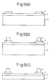
- an Al pad 3 is provided in the conventional manner (see Fig. 5(a)), and then an Au bump 4 (which is a conductive bump of about 35 ⁇ m high) is formed by using a plating or a bump bonder (see Fig. 5(b)). Thereafter, a back surface of the wafer 13 is abraded to have a desired thickness (for example, an original thickness of about 650 ⁇ m is abraded to about 50 ⁇ m). Thus the semiconductor element is completed.
- a laser beam for example, an ultraviolet laser beam
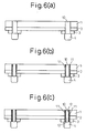
- a laser beam of a predetermined intensity is irradiated from above the semiconductor element 1 to a position corresponding to the Au bump to form a via-hole 10 of a proper size (for example, having a diameter of 10 ⁇ m or less) passing through the semiconductor element to reach the back surface of the Au bump 4 (see Fig. 6(a)).
- the Au bump 4 serves as a stopper for precisely controlling the boring process carried out by the laser beam.
- an insulation layer 11 is formed on the inner surface of the via-hole 10 by using CVD or a spin coater (see Fig. 6(b)).
- CVD tetraethoxysilane is vaporized to form an insulation layer of SiO 2 .
- a conductive cover film 12 is formed on the surface of the insulation layer 11.
- a thin semiconductor element according to the present invention is produced, which is suitably used for preparing a stacking type semiconductor device.
- Fig. 7 illustrates one embodiment of a semiconductor device constituted by stacking the semiconductor elements according to the present invention on a circuit board 14 having solder bumps 8.
- the semiconductor elements are electrically connected to each other by the connection structure according to the present invention.
- the semiconductor elements having the same dimension and structure are sequentially stacked to establish a direct electric connection between them, it is possible to obtain a semiconductor device large in capacity, small in size and thickness as well as responsive to a high-speed operation.
- the semiconductor elements having the same dimension and structure are sequentially stacked, even if the semiconductor element is heated, the thermal expansion of the respective semiconductor elements becomes approximately equal, whereby the electric connection between the semiconductor elements can be always maintained in a stable state.
Abstract
Description
- The present invention relates to a structure of a semiconductor element, a connection structure thereof and a semiconductor device formed by stacking such semiconductor elements. The present invention also relates to processes for making such semiconductor element and devices.
- Various packages have been known, in the prior art, for carrying semiconductor elements (semiconductor chips such as LSI). Of them, TCP (a tape carrier package) is widely used nowadays because it is suitable for a multi-pin structure having small-pitched connector terminals so that the reduction of a total device thickness and size could be realized as well as it is advantageous in view of the economical standpoint and the productivity.
- In general, a large capacity semiconductor device has been contemplated by stacking such semiconductor elements represented by TCP. In this case, since the semiconductor device should be small and thin, a connection structure is required which is capable of stacking as many as possible of the semiconductor elements in a predetermined height.
- Fig. 1 shows a conventional connection structure for a prior art stacking type semiconductor device. A
semiconductor element 1 hasAl pads 3 on acircuitry surface 2. On each of the Al pad, anAu bump 4 is formed for the electric connection with other semiconductor element 1'. This semiconductor element is integral with an interposer 9 consisting of acircuit layer 6, aninsulation layer 7 andsolder bumps 8 via an underfil layer 5 made of a resin (such as epoxy resin) to complete a stacking semiconductor device. Since this stacking semiconductor device is of a structure for connecting theAu bump 4 of thesemiconductor element 1 with thecircuit layer 6 of the interposer, thesolder bump 8 becomes a connection terminal for the connection with another stacking semiconductor device. - When such stacking semiconductor devices are stacked, as shown in Fig. 1, the semiconductor element l'of the other stacking semiconductor device is accommodated in a lower space of the interposer in the stacking semiconductor device, and the
solder bumps 8 are in contact with the circuit layer of the other stacking semiconductor device. - That is, in the prior art, the respective semiconductor element is mounted onto the interposer to form one package, which is then stacked on the other to provide a large-capacity stacked type semiconductor device while ensuring the electric connection between the respective semiconductor elements.
- According to the above-mentioned stacking of the packages, however, it is difficult to (1) reduce the size of the resultant semiconductor device as seen in a plan view although the increase in capacity is achievable or (2) satisfy the requirement for miniaturizing the semiconductor device even though a larger number of the packages are stacked.
- Also, if the interposer is used for stacking the semiconductor elements, a high-speed response becomes difficult and this limits the use of the semiconductor device.
- Therefore, recently, the stacking type semiconductor device is required to have a stack structure and/or a connection structure capable of realizing not only a large capacity, a small size and a small thickness but also a high-speed response.
- The present invention has been made in view of the above-mentioned requirements.
- Accordingly, an object of the present invention is to provide a semiconductor element involving an excellent stacking structure and/or a connection structure for semiconductor elements capable of realizing a large capacity, a small size and a small thickness as well as a high- speed response, and also a semiconductor device formed by stacking such semiconductor elements.
- The inventor of the present invention initially studied the prior art connection structure shown in Fig. 1 when solving the above-mentioned problems. As a result, it was noted that, if the interposer is eliminated from the prior art connection structure, it is possible to stack more semiconductor elements if the same height of the connection structure is to be maintained, or to further reduce the thickness of the semiconductor device if the same capacity of the semiconductor device is to be maintained, in addition to which, it is possible to respond to a high-speed operation so far as the interposer is eliminated. Based on this idea, the inventor diligently studied to obtain a connection structure capable of electrically interconnecting the semiconductor elements stacked to form a plurality of layers without using an interposer.
- According to an aspect of the present invention, there is provided a semiconductor element comprising: an element body having a first surface and a second, opposite surface; a conductive bump formed on the first surface of the element body; and the element body having a via hole penetrating from the conductive bump on the first surface to the second surface.
- An inner wall of the via hole is coated with an insulating layer and a conductive film, so that the conductive film is electrically connected to the conductive bump.
- The material of the conductive film is Au or Cu. The material of the insulating layer is SiO2.
- According to another aspect of the present invention, there is provided a connection structure comprising: a first semiconductor element having a first conductive bump; a second semiconductor element comprising: an element body having a first surface and a second, opposite surface; a second conductive bump formed on the first surface of the element body; and the element body having a via hole penetrating from the conductive bump on the first surface to the second surface; and
the first and second semiconductor elements are mutually arranged in such a manner that the first conductive bump is in contact with the second surface of the second semiconductor element at a position of the vial hole; and
means for electrically connecting the first conductive bump with the second conductive bump. - According to a further aspect of the present invention, there is provided a semiconductor device comprising a plurality of semiconductor elements stacked on one another, including at least:
- a first semiconductor element having a first and second, opposite surface thereof, and having a first conductive bump on the first surface;
- a second semiconductor element comprising: an element body having a first surface and a second, opposite surface; a second conductive bump formed on the first surface of the element body; and the element body having a via hole penetrating from the conductive bump on the first surface to the second surface;
- the first and second semiconductor elements are mutually arranged in such a manner that the first conductive bump is in contact with the second surface of the second semiconductor element at a position of the via hole; and
- means for electrically connecting the first conductive bump with the second conductive bump.
-
- According to a still further aspect of the present invention, there is provided a process for manufacturing a semiconductor element comprising the following steps of: forming a conductive bump on a first surface of a semiconductor element body; and forming a via hole which penetrates the element body from the conductive bump on the first surface to a second, opposite surface of the element body. The process further comprises the following steps of: coating an inner wall of the via hole with an insulating layer and a conductive film, so that the conductive bump is electrically connected to the conductive film.
- According to still further aspect of the present invention, there is provided a process for manufacturing a semiconductor device comprising a plurality of semiconductor elements stacked on one another, the process comprising the following steps of:
- preparing a plurality of semiconductor elements, the preparing step of each semiconductor element comprising: forming a conductive bump on a first surface of a semiconductor element body; forming a via hole which penetrates the element body from the conductive bump on the first surface to a second, opposite surface of the element body; and coating an inner wall of the via hole with a conductive film by means of an insulating layer so that the conductive bump is electrically connected to the conductive film.
- stacking at least two semiconductor elements, one on the other, in such a manner that the conductive bump of the one semiconductor element is in contact with the second surface of another semiconductor element at a position of the via hole so that the conductive bump of the one semiconductor element is electrically connected to a conductive bump of the other semiconductor element.
-
-
- Fig. 1 shows a prior art connection structure for semiconductor elements in the conventional stacking type semiconductor device;
- Fig. 2 shows one embodiment of a semiconductor element according to the present invention;
- Fig. 3 shows one embodiment of a via-hole;
- Fig. 4 shows the semiconductor elements stacked according to the present invention;
- Figs. 5(a) to 5(c) show the steps for producing the semiconductor element according to the present invention;
- Figs. 6(a) to 6(c) show the steps for forming via-holes, insulation layers and conductive cover films in the semiconductor element;
- Fig. 7 shows one embodiment of a semiconductor device stacking the semiconductor elements according to the present invention.
-
- The present invention will be described below with reference to the attached drawings.
- Fig. 2 shows one embodiment of a semiconductor element according to the present invention. In the
semiconductor element 1 shown in Fig. 2, via-holes 10 are formed, each of which passes through acircuitry surface 2 and reaches a back surface of an Au bump (conductive bump) 4 formed on anAl pad 3. This is a first characteristic of the present invention. As shown in Fig. 3, aconductive cover film 12 is formed on the inner surface of the via-hole 10 via aninsulation layer 11. - While the
conductive cover film 12 is preferably made of Au or Cu, another conductive metal or alloy may be used. While theinsulation layer 11 is preferably made of SiO2 because the insulation layer and the conductive cover film can be easily formed and the insulation layer can be brought into tight contact with the conductive cover film and a wafer, another insulation material may be used provided it satisfies such requirements. - As the
insulation cover film 12 is continuous with the conductive bump, it functions as a connection terminal when one semiconductor element is electrically connected to another semiconductor element. - One embodiment in which two semiconductor elements are stacked is illustrated in Fig. 4. As shown in Fig. 4, since a
conductive bump 4 of the one semiconductor elements (the upper one in the drawing) abuts a via-hole 10 of the other semiconductor element (the lower one in the drawing) and is in contact with theconductive cover film 12, theconductive bumps 4 of the upper and lowerconductive bumps 4 are connected to each other through theconductive cover film 12, whereby the electrical connection is directly made between the upper and lower semiconductor elements. - In such a manner, according to the present invention, it is possible to stack the semiconductor elements while ensuring the electrical connection between them without using the interposer. This is the second characteristic of the present invention.
- Then, a method will be described with reference to Figs. 5 and 6, for producing the semiconductor element, forming the via-holes in the semiconductor element and finally providing the conductive cover film.
- On a
circuitry surface 2 formed on a surface of a wafer 13 (for example, of 650 µm thick), anAl pad 3 is provided in the conventional manner (see Fig. 5(a)), and then an Au bump 4 (which is a conductive bump of about 35 µm high) is formed by using a plating or a bump bonder (see Fig. 5(b)). Thereafter, a back surface of thewafer 13 is abraded to have a desired thickness (for example, an original thickness of about 650 µm is abraded to about 50µm). Thus the semiconductor element is completed. - Next, while the
Au bump 4 is turned upside down so that theAu bump 4 directs downward, a laser beam (for example, an ultraviolet laser beam) of a predetermined intensity is irradiated from above thesemiconductor element 1 to a position corresponding to the Au bump to form a via-hole 10 of a proper size (for example, having a diameter of 10µm or less) passing through the semiconductor element to reach the back surface of the Au bump 4 (see Fig. 6(a)). - When the laser beam is irradiated, the
Au bump 4 serves as a stopper for precisely controlling the boring process carried out by the laser beam. - Then, an
insulation layer 11 is formed on the inner surface of the via-hole 10 by using CVD or a spin coater (see Fig. 6(b)). For example, by using CVD, tetraethoxysilane is vaporized to form an insulation layer of SiO2. Thereafter, by using a plating method or a sputtering method, aconductive cover film 12 is formed on the surface of theinsulation layer 11. - In this manner, a thin semiconductor element according to the present invention is produced, which is suitably used for preparing a stacking type semiconductor device.
- Fig. 7 illustrates one embodiment of a semiconductor device constituted by stacking the semiconductor elements according to the present invention on a
circuit board 14 having solder bumps 8. The semiconductor elements are electrically connected to each other by the connection structure according to the present invention. As a resin is filled in a gap between the adjacent semiconductor elements so that an integral structure is formed, it is possible to ensure the electrical connection between the semiconductor elements and also guarantee the strength, durability, thermal resistance or others of the semiconductor device. - According to the present invention, as the semiconductor elements having the same dimension and structure are sequentially stacked to establish a direct electric connection between them, it is possible to obtain a semiconductor device large in capacity, small in size and thickness as well as responsive to a high-speed operation.
- Also, according to the present invention, as the semiconductor elements having the same dimension and structure are sequentially stacked, even if the semiconductor element is heated, the thermal expansion of the respective semiconductor elements becomes approximately equal, whereby the electric connection between the semiconductor elements can be always maintained in a stable state.
- It should be understood by those skilled in the art that the foregoing description relates to only some preferred embodiments of the disclosed invention, and that various changes and modifications may be made to the invention without departing the sprit and scope thereof.
Claims (15)
- A semiconductor element comprising:an element body having a first surface and a second, opposite surface;a conductive bump formed on the first surface of the element body; andthe element body having a via hole penetrating from the conductive bump on the first surface to the second surface.
- A semiconductor element as set forth in claim 1, wherein an inner wall of the via hole is coated with an insulating layer and also coated with a conductive film, and the conductive film is electrically connected to the conductive bump.
- A semiconductor element as set forth in claim 2, wherein a material of the conductive film is Au or Cu.
- A semiconductor element as set forth in claim 2, wherein a material of the insulating layer is SiO2.
- A connection structure comprising:a first semiconductor element having a first conductive bump;a second semiconductor element comprising:an element body having a first surface and a second, opposite surface;a second conductive bump formed on the first surface of the element body; andthe element body having a via hole penetrating from the conductive bump on the first surface to the second surface; and
the first and second semiconductor elements are mutually arranged in such a manner that the first conductive bump is in contact with the second surface of the second semiconductor element at a position of the via hole; andmeans for electrically connecting the first conductive bump with the second conductive bump. - A connection structure as set forth in claim 5, wherein the electrically connecting means comprises a conductive film which is coated on an inner wall of the via hole of the second semiconductor element, said conduction film is coated on an insulating layer, so that the conductive film electrically connects the first conductive bump with the second conductive bump.
- A connection structure as set forth in claim 6, wherein a material of the conductive film is Au or Cu.
- A connection structure as set forth in claim 6, wherein a material of the insulating layer is SiO2.
- A semiconductor device comprising a plurality of stacked semiconductor elements, including at least:a first semiconductor element having a first and second, opposite surface thereof, and having a first conductive bump on the first surface;a second semiconductor element comprising:an element body having a first surface and a second, opposite surface;a second conductive bump formed on the first surface of the element body; andthe element body having a via hole penetrating from the conductive bump on the first surface to the second surface; and
the first and second semiconductor elements are mutually arranged in such a manner that the first conductive bump is in contact with the second surface of the second semiconductor element at a position of the vial hole; and
means for electrically connecting the first conductive bump with the second conductive bump. - A semiconductor device as set forth in claim 9, wherein the electrically connecting means comprises a conductive film which is coated on an inner wall of the via hole of the second semiconductor element, said conductive film is coated on an insulating layer, so that the conductive film electrically connects mutually the first conductive bump with the second conductive bump.
- A semiconductor device as set forth in claim 10, wherein a material of the conductive film is Au or Cu.
- A semiconductor device as set forth in claim 10, wherein a material of the insulating layer is SiO2.
- A process for manufacturing a semiconductor element comprising the following steps of:forming a conductive bump on a first surface of a semiconductor element body; andforming a via hole which penetrates the element body from the conductive bump on the first surface to a second, opposite surface of the element body.
- A process as set forth in claim 13 further comprising the following steps of:coating an inner wall of the via hole with a conductive film by means of an insulating layer so that the conductive bump is electrically connected to the conductive film.
- A process for manufacturing a semiconductor device comprising a plurality of semiconductor elements stacked on one another, the process comprising the following steps of:preparing a plurality of semiconductor elements, the preparing step of each semiconductor element comprising;forming a conductive bump on a first surface of a semiconductor element body;forming a via hole which penetrates the element body from the conductive bump on the first surface to a second, opposite surface of the element body; andcoating an inner wall of the via hole with an insulating layer, and a conductive film, so that the conductive bump is electrically connected to the conductive film;stacking at least two semiconductor elements, one on the other, in such a manner that the conductive bump of the one semiconductor element is in contact with the second surface of another semiconductor element at a position.of the via hole so that the conductive bump of the one semiconductor element is electrically connected to a conductive bump of the other semiconductor element.
Applications Claiming Priority (2)
| Application Number | Priority Date | Filing Date | Title |
|---|---|---|---|
| JP2001109118A JP2002305282A (en) | 2001-04-06 | 2001-04-06 | Semiconductor element and structure for connecting the same, and semiconductor device with stacked semiconductor elements |
| JP2001109118 | 2001-04-06 |
Publications (2)
| Publication Number | Publication Date |
|---|---|
| EP1248295A2 true EP1248295A2 (en) | 2002-10-09 |
| EP1248295A3 EP1248295A3 (en) | 2005-07-13 |
Family
ID=18961123
Family Applications (1)
| Application Number | Title | Priority Date | Filing Date |
|---|---|---|---|
| EP02007769A Withdrawn EP1248295A3 (en) | 2001-04-06 | 2002-04-05 | Semiconductor element, connection structure thereof, semiconductor device using a plurality of such elements and processes for making the same |
Country Status (3)
| Country | Link |
|---|---|
| US (1) | US20020145191A1 (en) |
| EP (1) | EP1248295A3 (en) |
| JP (1) | JP2002305282A (en) |
Cited By (5)
| Publication number | Priority date | Publication date | Assignee | Title |
|---|---|---|---|---|
| WO2004038798A2 (en) * | 2002-10-22 | 2004-05-06 | Unitive International Limited | Stacked electronic structures including offset substrates |
| EP1418617A2 (en) * | 2002-11-05 | 2004-05-12 | Shinko Electric Co. Ltd. | Semiconductor device and method of manufacturing the same |
| EP1427006A1 (en) * | 2002-12-03 | 2004-06-09 | Shinko Electric Industries Co., Ltd. | Electronic parts packaging structure and method of manufacturing the same |
| EP1777742A3 (en) * | 2005-10-18 | 2008-08-20 | Shinko Electric Industries Co., Ltd. | Semiconductor chip with through via and method of manufacturing the semiconductor chip |
| US8674494B2 (en) | 2011-08-31 | 2014-03-18 | Samsung Electronics Co., Ltd. | Semiconductor package having supporting plate and method of forming the same |
Families Citing this family (16)
| Publication number | Priority date | Publication date | Assignee | Title |
|---|---|---|---|---|
| JP3646719B2 (en) * | 2003-06-19 | 2005-05-11 | セイコーエプソン株式会社 | Semiconductor device and manufacturing method thereof, circuit board, and electronic apparatus |
| JP4340517B2 (en) | 2003-10-30 | 2009-10-07 | Okiセミコンダクタ株式会社 | Semiconductor device and manufacturing method thereof |
| CN100511672C (en) * | 2004-03-25 | 2009-07-08 | 日本电气株式会社 | Chip stacking semiconductor device |
| JP4577687B2 (en) * | 2005-03-17 | 2010-11-10 | エルピーダメモリ株式会社 | Semiconductor device |
| JP2007067082A (en) * | 2005-08-30 | 2007-03-15 | Disco Abrasive Syst Ltd | Perforation method of wafer |
| CN100568502C (en) | 2005-09-06 | 2009-12-09 | 日本电气株式会社 | Semiconductor device |
| JP2007305955A (en) * | 2006-04-10 | 2007-11-22 | Toshiba Corp | Semiconductor device and its manufacturing process |
| JP2008068292A (en) * | 2006-09-14 | 2008-03-27 | Disco Abrasive Syst Ltd | Method for machining via-hole |
| JP4773307B2 (en) | 2006-09-15 | 2011-09-14 | Okiセミコンダクタ株式会社 | Manufacturing method of semiconductor device |
| JP2008073711A (en) * | 2006-09-20 | 2008-04-03 | Disco Abrasive Syst Ltd | Machining method of via hole |
| JP2008073740A (en) * | 2006-09-22 | 2008-04-03 | Disco Abrasive Syst Ltd | Via hole machining method |
| JP2008155274A (en) * | 2006-12-26 | 2008-07-10 | Disco Abrasive Syst Ltd | Method of machining wafer |
| JP2008212999A (en) * | 2007-03-06 | 2008-09-18 | Disco Abrasive Syst Ltd | Laser beam machining apparatus |
| JP4939452B2 (en) * | 2008-02-07 | 2012-05-23 | ラピスセミコンダクタ株式会社 | Manufacturing method of semiconductor device |
| US8390130B1 (en) * | 2011-01-06 | 2013-03-05 | Amkor Technology, Inc. | Through via recessed reveal structure and method |
| KR101918609B1 (en) | 2012-01-11 | 2018-11-14 | 삼성전자 주식회사 | Integrated circuit device |
Citations (1)
| Publication number | Priority date | Publication date | Assignee | Title |
|---|---|---|---|---|
| EP1061578A1 (en) * | 1998-12-16 | 2000-12-20 | Seiko Epson Corporation | Semiconductor chip, semiconductor device, circuit board and electronic equipment and production methods for them |
Family Cites Families (7)
| Publication number | Priority date | Publication date | Assignee | Title |
|---|---|---|---|---|
| GB9018766D0 (en) * | 1990-08-28 | 1990-10-10 | Lsi Logic Europ | Stacking of integrated circuits |
| US5229647A (en) * | 1991-03-27 | 1993-07-20 | Micron Technology, Inc. | High density data storage using stacked wafers |
| JP2622038B2 (en) * | 1991-06-03 | 1997-06-18 | シャープ株式会社 | Semiconductor device and manufacturing method thereof |
| WO1996013062A1 (en) * | 1994-10-19 | 1996-05-02 | Ceram Incorporated | Apparatus and method of manufacturing stacked wafer array |
| JP3186941B2 (en) * | 1995-02-07 | 2001-07-11 | シャープ株式会社 | Semiconductor chips and multi-chip semiconductor modules |
| US6222276B1 (en) * | 1998-04-07 | 2001-04-24 | International Business Machines Corporation | Through-chip conductors for low inductance chip-to-chip integration and off-chip connections |
| US6122187A (en) * | 1998-11-23 | 2000-09-19 | Micron Technology, Inc. | Stacked integrated circuits |
-
2001
- 2001-04-06 JP JP2001109118A patent/JP2002305282A/en active Pending
-
2002
- 2002-04-02 US US10/114,518 patent/US20020145191A1/en not_active Abandoned
- 2002-04-05 EP EP02007769A patent/EP1248295A3/en not_active Withdrawn
Patent Citations (1)
| Publication number | Priority date | Publication date | Assignee | Title |
|---|---|---|---|---|
| EP1061578A1 (en) * | 1998-12-16 | 2000-12-20 | Seiko Epson Corporation | Semiconductor chip, semiconductor device, circuit board and electronic equipment and production methods for them |
Cited By (17)
| Publication number | Priority date | Publication date | Assignee | Title |
|---|---|---|---|---|
| WO2004038798A3 (en) * | 2002-10-22 | 2004-07-29 | Unitive Int Ltd | Stacked electronic structures including offset substrates |
| US7495326B2 (en) | 2002-10-22 | 2009-02-24 | Unitive International Limited | Stacked electronic structures including offset substrates |
| WO2004038798A2 (en) * | 2002-10-22 | 2004-05-06 | Unitive International Limited | Stacked electronic structures including offset substrates |
| EP1801866A2 (en) * | 2002-11-05 | 2007-06-27 | Shinko Electric Industries Co., Ltd. | Semiconductor device and method of manufacturing the same |
| US7507602B2 (en) | 2002-11-05 | 2009-03-24 | Shinko Electric Industries Co., Ltd. | Semiconductor device and method of manufacturing the same |
| US6958544B2 (en) | 2002-11-05 | 2005-10-25 | Shinko Electric Industries Co., Ltd. | Semiconductor device and method of manufacturing the same |
| EP1418617A3 (en) * | 2002-11-05 | 2004-05-26 | Shinko Electric Co. Ltd. | Semiconductor device and method of manufacturing the same |
| EP1801866A3 (en) * | 2002-11-05 | 2007-12-19 | Shinko Electric Industries Co., Ltd. | Semiconductor device and method of manufacturing the same |
| EP1418617A2 (en) * | 2002-11-05 | 2004-05-12 | Shinko Electric Co. Ltd. | Semiconductor device and method of manufacturing the same |
| US6943442B2 (en) | 2002-12-03 | 2005-09-13 | Shinko Electric Industries Co., Ltd. | Electronic parts packaging structure having mutually connected electronic parts that are buried in a insulating film |
| US7084009B2 (en) | 2002-12-03 | 2006-08-01 | Shinko Electric Industries Co., Ltd. | Method of manufacturing a packaging structure for electronic parts buried in an insulating film formed on the electronic parts and a wiring substrate |
| EP1427006A1 (en) * | 2002-12-03 | 2004-06-09 | Shinko Electric Industries Co., Ltd. | Electronic parts packaging structure and method of manufacturing the same |
| EP1777742A3 (en) * | 2005-10-18 | 2008-08-20 | Shinko Electric Industries Co., Ltd. | Semiconductor chip with through via and method of manufacturing the semiconductor chip |
| US7576004B2 (en) | 2005-10-18 | 2009-08-18 | Shinko Electric Industries Co., Ltd. | Semiconductor chip and method of manufacturing semiconductor chip |
| US7592700B2 (en) | 2005-10-18 | 2009-09-22 | Shinko Electric Industries Co., Ltd. | Semiconductor chip and method of manufacturing semiconductor chip |
| US8674494B2 (en) | 2011-08-31 | 2014-03-18 | Samsung Electronics Co., Ltd. | Semiconductor package having supporting plate and method of forming the same |
| US9412720B2 (en) | 2011-08-31 | 2016-08-09 | Samsung Electronics Co., Ltd. | Semiconductor package having supporting plate and method of forming the same |
Also Published As
| Publication number | Publication date |
|---|---|
| US20020145191A1 (en) | 2002-10-10 |
| EP1248295A3 (en) | 2005-07-13 |
| JP2002305282A (en) | 2002-10-18 |
Similar Documents
| Publication | Publication Date | Title |
|---|---|---|
| EP1248295A2 (en) | Semiconductor element, connection structure thereof, semiconductor device using a plurality of such elements and processes for making the same | |
| US6022758A (en) | Process for manufacturing solder leads on a semiconductor device package | |
| US7531890B2 (en) | Multi-chip package (MCP) with a conductive bar and method for manufacturing the same | |
| JP2819284B2 (en) | Semiconductor package substrate, method of manufacturing the same, and stacked semiconductor package using the substrate | |
| EP0208494B1 (en) | Method of fabricating a semiconductor apparatus comprising two semiconductor devices | |
| US6413798B2 (en) | Package having very thin semiconductor chip, multichip module assembled by the package, and method for manufacturing the same | |
| US6800505B2 (en) | Semiconductor device including edge bond pads and related methods | |
| KR100282285B1 (en) | Stacked multichip module and manufacturing method thereof | |
| US5838061A (en) | Semiconductor package including a semiconductor chip adhesively bonded thereto | |
| US6469260B2 (en) | Wiring boards, semiconductor devices and their production processes | |
| US7226809B2 (en) | Semiconductor devices and semiconductor device components with peripherally located, castellated contacts, assemblies and packages including such semiconductor devices or packages and associated methods | |
| US7706148B2 (en) | Stack structure of circuit boards embedded with semiconductor chips | |
| JP2017038075A (en) | Stackable molded ultra small electronic package including area array unit connector | |
| US20030122253A1 (en) | Wafer levelpackaging and chip structure | |
| JP2003163324A (en) | Unit semiconductor device and manufacturing method thereof, and three-dimensional laminated semiconductor device | |
| US20040135243A1 (en) | Semiconductor device, its manufacturing method and electronic device | |
| US20020070446A1 (en) | Semiconductor device and method for the production thereof | |
| US5863812A (en) | Process for manufacturing a multi layer bumped semiconductor device | |
| TW550768B (en) | Flip-chip on film assembly for ball grid array packages | |
| US20020093093A1 (en) | Semiconductor package with stacked dies | |
| US20040012941A1 (en) | Low profile stacked multi-chip package and method of forming same | |
| JP2004146728A (en) | Semiconductor device and its manufacturing method | |
| JPH09270490A (en) | Connecting construction, connecting method, and semiconductor device and its manufacture | |
| US20090045444A1 (en) | Integrated device and circuit system | |
| KR20050027384A (en) | Chip size package having rerouting pad and stack thereof |
Legal Events
| Date | Code | Title | Description |
|---|---|---|---|
| PUAI | Public reference made under article 153(3) epc to a published international application that has entered the european phase |
Free format text: ORIGINAL CODE: 0009012 |
|
| 17P | Request for examination filed |
Effective date: 20020405 |
|
| AK | Designated contracting states |
Kind code of ref document: A2 Designated state(s): AT BE CH CY DE DK ES FI FR GB GR IE IT LI LU MC NL PT SE TR |
|
| AX | Request for extension of the european patent |
Free format text: AL;LT;LV;MK;RO;SI |
|
| PUAL | Search report despatched |
Free format text: ORIGINAL CODE: 0009013 |
|
| AK | Designated contracting states |
Kind code of ref document: A3 Designated state(s): AT BE CH CY DE DK ES FI FR GB GR IE IT LI LU MC NL PT SE TR |
|
| AX | Request for extension of the european patent |
Extension state: AL LT LV MK RO SI |
|
| AKX | Designation fees paid |
Designated state(s): CH DE LI |
|
| STAA | Information on the status of an ep patent application or granted ep patent |
Free format text: STATUS: THE APPLICATION IS DEEMED TO BE WITHDRAWN |
|
| 18D | Application deemed to be withdrawn |
Effective date: 20100427 |