EP1262990A1 - Memory architecture for supporting concurrent access of different types - Google Patents
Memory architecture for supporting concurrent access of different types Download PDFInfo
- Publication number
- EP1262990A1 EP1262990A1 EP02004649A EP02004649A EP1262990A1 EP 1262990 A1 EP1262990 A1 EP 1262990A1 EP 02004649 A EP02004649 A EP 02004649A EP 02004649 A EP02004649 A EP 02004649A EP 1262990 A1 EP1262990 A1 EP 1262990A1
- Authority
- EP
- European Patent Office
- Prior art keywords
- column
- access
- memory
- write
- write access
- Prior art date
- Legal status (The legal status is an assumption and is not a legal conclusion. Google has not performed a legal analysis and makes no representation as to the accuracy of the status listed.)
- Withdrawn
Links
Images

Classifications
-
- G—PHYSICS
- G11—INFORMATION STORAGE
- G11C—STATIC STORES
- G11C7/00—Arrangements for writing information into, or reading information out from, a digital store
-
- G—PHYSICS
- G11—INFORMATION STORAGE
- G11C—STATIC STORES
- G11C8/00—Arrangements for selecting an address in a digital store
- G11C8/12—Group selection circuits, e.g. for memory block selection, chip selection, array selection
-
- G—PHYSICS
- G11—INFORMATION STORAGE
- G11C—STATIC STORES
- G11C11/00—Digital stores characterised by the use of particular electric or magnetic storage elements; Storage elements therefor
- G11C11/21—Digital stores characterised by the use of particular electric or magnetic storage elements; Storage elements therefor using electric elements
- G11C11/34—Digital stores characterised by the use of particular electric or magnetic storage elements; Storage elements therefor using electric elements using semiconductor devices
- G11C11/40—Digital stores characterised by the use of particular electric or magnetic storage elements; Storage elements therefor using electric elements using semiconductor devices using transistors
- G11C11/401—Digital stores characterised by the use of particular electric or magnetic storage elements; Storage elements therefor using electric elements using semiconductor devices using transistors forming cells needing refreshing or charge regeneration, i.e. dynamic cells
- G11C11/4063—Auxiliary circuits, e.g. for addressing, decoding, driving, writing, sensing or timing
- G11C11/407—Auxiliary circuits, e.g. for addressing, decoding, driving, writing, sensing or timing for memory cells of the field-effect type
- G11C11/4076—Timing circuits
-
- G—PHYSICS
- G11—INFORMATION STORAGE
- G11C—STATIC STORES
- G11C11/00—Digital stores characterised by the use of particular electric or magnetic storage elements; Storage elements therefor
- G11C11/21—Digital stores characterised by the use of particular electric or magnetic storage elements; Storage elements therefor using electric elements
- G11C11/34—Digital stores characterised by the use of particular electric or magnetic storage elements; Storage elements therefor using electric elements using semiconductor devices
- G11C11/40—Digital stores characterised by the use of particular electric or magnetic storage elements; Storage elements therefor using electric elements using semiconductor devices using transistors
- G11C11/401—Digital stores characterised by the use of particular electric or magnetic storage elements; Storage elements therefor using electric elements using semiconductor devices using transistors forming cells needing refreshing or charge regeneration, i.e. dynamic cells
- G11C11/4063—Auxiliary circuits, e.g. for addressing, decoding, driving, writing, sensing or timing
- G11C11/407—Auxiliary circuits, e.g. for addressing, decoding, driving, writing, sensing or timing for memory cells of the field-effect type
- G11C11/409—Read-write [R-W] circuits
- G11C11/4096—Input/output [I/O] data management or control circuits, e.g. reading or writing circuits, I/O drivers or bit-line switches
-
- G—PHYSICS
- G11—INFORMATION STORAGE
- G11C—STATIC STORES
- G11C7/00—Arrangements for writing information into, or reading information out from, a digital store
- G11C7/10—Input/output [I/O] data interface arrangements, e.g. I/O data control circuits, I/O data buffers
- G11C7/1075—Input/output [I/O] data interface arrangements, e.g. I/O data control circuits, I/O data buffers for multiport memories each having random access ports and serial ports, e.g. video RAM
-
- G—PHYSICS
- G11—INFORMATION STORAGE
- G11C—STATIC STORES
- G11C2207/00—Indexing scheme relating to arrangements for writing information into, or reading information out from, a digital store
- G11C2207/002—Isolation gates, i.e. gates coupling bit lines to the sense amplifier
-
- G—PHYSICS
- G11—INFORMATION STORAGE
- G11C—STATIC STORES
- G11C2207/00—Indexing scheme relating to arrangements for writing information into, or reading information out from, a digital store
- G11C2207/10—Aspects relating to interfaces of memory device to external buses
- G11C2207/104—Embedded memory devices, e.g. memories with a processing device on the same die or ASIC memory designs
Definitions
- the present invention relates generally to memory circuits, and more particularly, to a memory architecture for supporting concurrent access of different types.
- a typical embedded dynamic random access memory has a data width of 128 bits, which is divided into four 32-bit words.
- DRAM embedded dynamic random access memory
- There are four blocks e.g., BLOCK0, BLOCK1, BLOCK2, BLOCK3 that access this memory.
- the blocks use the same row space but different column spaces for memory access.
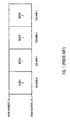
- FIG. 1 illustrates a prior art memory configuration.
- This memory architecture allows for concurrent access to all four columns when the access type is the same (i.e., when the operation for all four columns is all a read operation or when all the operation for all four columns is all a write operation).
- This restriction is referred to as an access-type restriction (i.e., only common access types can be performed concurrently).
- the access-type restriction incurs a significant time penalty. For example, when three of the four columns are of access type one and the fourth column is of access type two, two separate accesses or transfers are required. In other words, columns has with different access types cannot be accesses concurrently, but instead must be performed in sequential order. As can be appreciated, the access type restriction undesirably increases the time for memory accesses.
- CMOS synchronous SRAM model TC59SM816 available from Toshiba, Inc.
- a memory architecture for supporting mixed-mode memory accesses.
- a common row address is provided.
- a first column address for accessing a first column and a second column address for accessing a second column are provided.
- a first write control signal for specifying one of a write access and a read access for the first column, and a second write control signal for specifying one of a write access and a read access for the second column are also provided.
- the memory architecture responsive to these input signals, supports concurrent mixed-mode memory accesses to the first column and a write access to the second column.
- An individual write enable control signal is provided for each column. For example, when there are four columns (e.g., column_0, column_1, column_2, and column_3), there are four write enable control signals, where there is one write enable control signal corresponding to each column.
- the memory architecture of the present invention removes the access-type restriction and allows concurrent mixed-mode memory accesses.
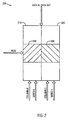
- FIG. 2 illustrates a memory architecture 200 that supports mixed-mode accesses according to one embodiment of the present invention can be utilized.
- the memory architecture 200 includes at least two columns (e.g., a first column 210 and a second column 220). According to the memory architecture 200 of the present invention, the write control signal applies to individual columns.
- each column receives an individual column signal and an individual write control signal.
- the first column 210 receives a COLUMN0 signal and a WRITE0 signal.
- the second column 220 receives a COLUMN1 signal and a WRITE1 signal. Since the write control signal is applied to individual columns, a first addressed area 250 can be selected for a read operation while a second addressed area 260 can be selected concurrently for a write operation.
- the row and column are selected by decoding address, RAS, and CAS. It is noted that unlike the prior art architecture that requires separate accesses to read and write to different columns in the same row, the architecture of the present invention allows different access types (e.g., one read operation and a write operation) on different columns in the same row in a concurrent fashion. In this regard, data is either written to or read from the addressed area (e.g., area 250 or area 260) based on the condition of the write enable signal (also referred to as a write control signal).
- the write enable signal also referred to as a write control signal
- the minimum access time be equal to the longer of the two access type minimum access times for mixed-mode accesses. For example, consider a situation where a write access is one clock cycle longer than the read access. A first block (block_0) can perform a write, while the second, third and fourth blocks (block_1, block_2, and block_3) perform a read operation. The total access time is the length of time of the write access since the write access takes longer than the read access.
- the prior art memory architecture assigns each block in the data path a contiguous one-dimensional chunk of memory.
- the memory architecture of the present invention assigns the blocks the same row space, but assigns each block a different column space.
- One advantage of the memory architecture of the present invention is that the blocks can access the memory concurrently instead of competing for memory access.
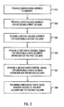
- FIG. 3 is a flow chart illustrating the processing steps for a mixed-mode memory access in accordance with one embodiment of the present invention.
- a common row address is provided to the memory.
- a first column address for accessing a first column is provided to the memory.
- a second column address for accessing a second column is provided to the memory.
- a first write control signal for specifying one of a write access and a read access for the first column is provided to the memory.
- a second write control signal for specifying one of a write access and a read access for the second column is provided to the memory.
- the memory architecture provides concurrent mixed-mode memory accesses to the first column and the second column.
- the memory architecture can provide a concurrent read access to the first column and a write access to the second column.
- the memory architecture can provide concurrent write access to the first column and a read access to the second column. It is to be appreciated that the number of columns that are utilized may be varied to suit a particular application. It is further noted that a read access may be granted to any sub-set (may be none of the columns) of these columns and a write access may be granted to any sub-set (may be none of the columns) at the same time.
- the memory control signals can be generated by a functional block that requires memory access, a memory controller circuit, or a combination thereof.
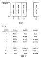
- FIG. 5 illustrates an exemplary memory configuration 510 in accordance with one embodiment of the present invention in which different column spaces may be assigned to different functional blocks.
- the memory configuration 510 includes a plurality of column spaces that may be assigned to a particular functional block. For example, a first column space 520 is assigned to a first functional block (BLOCK_1), a second column space 530 is assigned to a second functional block (BLOCK_2), a third column space 540 is assigned to a third functional block (BLOCK_1), and Nth column space 550 is assigned to an Nth functional block (BLOCK_N), etc.
- Each functional block may perform one or more functions. These functional blocks require memory access. Examples of functional blocks can be, for example, but is not limited to, a direct memory access (DMA) functional block, a processor, a video processor, a cache controller, decompression blocks, and datapath blocks. The functional blocks can be, for example, disposed in an application specific integrated circuit (ASIC).
- DMA direct memory access
- ASIC application specific integrated circuit
- the memory configuration 510 assigns each functional block the same row space, but a different column space, thereby supporting concurrent access by all the functional blocks to the memory. In this manner, the time penalty, associated with the access-type restriction, is avoided.
- FIG. 6 illustrates an exemplary vertical address space allocation 610 in accordance with one embodiment of the present invention.
- additional address locations are employed (e.g., those locations denoted "trash") to facilitate pipelining. It is noted that the overhead for supporting pipelining is minimal.
- FIG. 4 illustrates the memory 410 of the present invention embedded in an application specific integrated circuit 400.
- the ASIC 400 includes an embedded memory 410 that can be configured in accordance with the teachings of the present invention.
- the ASIC 400 can have a plurality of functional blocks 430 that require access to the memory 410.
- a data path 450 is provided to transfer data between the functional blocks 430 and the memory 410. It is noted that the width of the data path is partitioned with each functional block having a portion thereof, such as a first portion 434 and a second portion 438.
- An address and control bus 460 is provided for communicating address and other control signals to the memory 410.
- Each functional block 430 also provides an individual column address strobe (CAS) signal and a write enable or write control signal.
- CAS column address strobe
- R/W_B0.. RIW_BN are provided by the functional blocks 430 to the memory 410
Abstract
A memory architecture (200) for supporting mixed-mode memory accesses. A
common row address is provided. A first column address for accessing a first
column (210) and a second column address for accessing a second column (220) are
provided. A first write control signal for specifying one of a write access and a read
access for the first column (210), and a second write control signal for specifying one
of a write access and a read access for the second column (220) are also provided.
The memory architecture (200), responsive to these input signals, supports concurrent
mixed-mode memory accesses to the first column (210) and a write access to the
second column (220).
Description
- The present invention relates generally to memory circuits, and more particularly, to a memory architecture for supporting concurrent access of different types.
- A typical embedded dynamic random access memory (DRAM) has a data width of 128 bits, which is divided into four 32-bit words. Consider the case, where there are four blocks (e.g., BLOCK0, BLOCK1, BLOCK2, BLOCK3) that access this memory. The blocks use the same row space but different column spaces for memory access. FIG. 1 illustrates a prior art memory configuration.
- This memory architecture allows for concurrent access to all four columns when the access type is the same (i.e., when the operation for all four columns is all a read operation or when all the operation for all four columns is all a write operation). This restriction is referred to as an access-type restriction (i.e., only common access types can be performed concurrently).
- Unfortunately, the access-type restriction incurs a significant time penalty. For example, when three of the four columns are of access type one and the fourth column is of access type two, two separate accesses or transfers are required. In other words, columns has with different access types cannot be accesses concurrently, but instead must be performed in sequential order. As can be appreciated, the access type restriction undesirably increases the time for memory accesses.
- An example of a memory configuration that has this access-type restriction is the CMOS synchronous SRAM model TC59SM816 available from Toshiba, Inc.
- Consequently, it would be desirable for a memory architecture that allows for supporting concurrent memory access of different types.
- Based on the foregoing, there remains a need for a memory architecture for supporting concurrent access of different types.
- According to one embodiment of the present invention, a memory architecture for supporting mixed-mode memory accesses. A common row address is provided. A first column address for accessing a first column and a second column address for accessing a second column are provided. A first write control signal for specifying one of a write access and a read access for the first column, and a second write control signal for specifying one of a write access and a read access for the second column are also provided. The memory architecture, responsive to these input signals, supports concurrent mixed-mode memory accesses to the first column and a write access to the second column.
- The present invention is illustrated by way of example, and not by way of limitation, in the figures of the accompanying drawings and in which like reference numerals refer to similar elements.
- FIG. 1 illustrates a prior art memory configuration.
- FIG. 2 illustrates a memory architecture that supports mixed-mode accesses according to one embodiment of the present invention can be utilized.
- FIG. 3 is a flow chart illustrating the processing step for a mixed-mode memory access in accordance with one embodiment of the present invention.
- FIG. 4 illustrates the memory of the present invention embedded in an application specific integrated circuit.
- FIG. 5 illustrates an exemplary memory configuration in accordance with one embodiment of the present invention in which different column spaces may be assigned to different functional blocks.
- FIG. 6 illustrates an exemplary vertical address space allocation in accordance with one embodiment of the present invention.
-
- A memory architecture for supporting mixed-mode memory access is described. In the following description, for the purposes of explanation, numerous specific details are set forth in order to provide a thorough understanding of the present invention. It will be apparent, however, to one skilled in the art that the present invention may be practiced without these specific details. In other instances, well-known structures and devices are shown in block diagram form in order to avoid unnecessarily obscuring the present invention.
- An individual write enable control signal is provided for each column. For example, when there are four columns (e.g., column_0, column_1, column_2, and column_3), there are four write enable control signals, where there is one write enable control signal corresponding to each column.
- The memory architecture of the present invention removes the access-type restriction and allows concurrent mixed-mode memory accesses.
- FIG. 2 illustrates a
memory architecture 200 that supports mixed-mode accesses according to one embodiment of the present invention can be utilized. Thememory architecture 200 includes at least two columns (e.g., afirst column 210 and a second column 220). According to thememory architecture 200 of the present invention, the write control signal applies to individual columns. - Specifically, each column receives an individual column signal and an individual write control signal. For example, the
first column 210 receives a COLUMN0 signal and a WRITE0 signal. Similarly, the second column 220 receives a COLUMN1 signal and a WRITE1 signal. Since the write control signal is applied to individual columns, a first addressedarea 250 can be selected for a read operation while a second addressed area 260 can be selected concurrently for a write operation. - The row and column are selected by decoding address, RAS, and CAS. It is noted that unlike the prior art architecture that requires separate accesses to read and write to different columns in the same row, the architecture of the present invention allows different access types (e.g., one read operation and a write operation) on different columns in the same row in a concurrent fashion. In this regard, data is either written to or read from the addressed area (e.g.,
area 250 or area 260) based on the condition of the write enable signal (also referred to as a write control signal). - It is important that the minimum access time be equal to the longer of the two access type minimum access times for mixed-mode accesses. For example, consider a situation where a write access is one clock cycle longer than the read access. A first block (block_0) can perform a write, while the second, third and fourth blocks (block_1, block_2, and block_3) perform a read operation. The total access time is the length of time of the write access since the write access takes longer than the read access.
- It is noted that this approach yields a timesaving as compared to the prior art that holds off any of the blocks.
- The prior art memory architecture assigns each block in the data path a contiguous one-dimensional chunk of memory. In contrast, the memory architecture of the present invention assigns the blocks the same row space, but assigns each block a different column space. One advantage of the memory architecture of the present invention is that the blocks can access the memory concurrently instead of competing for memory access.
- FIG. 3 is a flow chart illustrating the processing steps for a mixed-mode memory access in accordance with one embodiment of the present invention. In
step 310, a common row address is provided to the memory. Instep 320, a first column address for accessing a first column is provided to the memory. Instep 330, a second column address for accessing a second column is provided to the memory. Instep 340, a first write control signal for specifying one of a write access and a read access for the first column is provided to the memory. Instep 350, a second write control signal for specifying one of a write access and a read access for the second column is provided to the memory. - In
step 360, the memory architecture provides concurrent mixed-mode memory accesses to the first column and the second column. For example, the memory architecture can provide a concurrent read access to the first column and a write access to the second column. Similarly, the memory architecture can provide concurrent write access to the first column and a read access to the second column. It is to be appreciated that the number of columns that are utilized may be varied to suit a particular application. It is further noted that a read access may be granted to any sub-set (may be none of the columns) of these columns and a write access may be granted to any sub-set (may be none of the columns) at the same time. - It is noted that the memory control signals can be generated by a functional block that requires memory access, a memory controller circuit, or a combination thereof.
- FIG. 5 illustrates an exemplary memory configuration 510 in accordance with one embodiment of the present invention in which different column spaces may be assigned to different functional blocks. The memory configuration 510 includes a plurality of column spaces that may be assigned to a particular functional block. For example, a
first column space 520 is assigned to a first functional block (BLOCK_1), asecond column space 530 is assigned to a second functional block (BLOCK_2), athird column space 540 is assigned to a third functional block (BLOCK_1), andNth column space 550 is assigned to an Nth functional block (BLOCK_N), etc. - Each functional block may perform one or more functions. These functional blocks require memory access. Examples of functional blocks can be, for example, but is not limited to, a direct memory access (DMA) functional block, a processor, a video processor, a cache controller, decompression blocks, and datapath blocks. The functional blocks can be, for example, disposed in an application specific integrated circuit (ASIC).
- It is noted that the memory configuration 510 assigns each functional block the same row space, but a different column space, thereby supporting concurrent access by all the functional blocks to the memory. In this manner, the time penalty, associated with the access-type restriction, is avoided.
- FIG. 6 illustrates an exemplary vertical
address space allocation 610 in accordance with one embodiment of the present invention. Preferably, additional address locations are employed (e.g., those locations denoted "trash") to facilitate pipelining. It is noted that the overhead for supporting pipelining is minimal. - FIG. 4 illustrates the
memory 410 of the present invention embedded in an application specificintegrated circuit 400. TheASIC 400 includes an embeddedmemory 410 that can be configured in accordance with the teachings of the present invention. TheASIC 400 can have a plurality offunctional blocks 430 that require access to thememory 410. Adata path 450 is provided to transfer data between thefunctional blocks 430 and thememory 410. It is noted that the width of the data path is partitioned with each functional block having a portion thereof, such as afirst portion 434 and asecond portion 438. - An address and control bus 460 is provided for communicating address and other control signals to the
memory 410. Eachfunctional block 430 also provides an individual column address strobe (CAS) signal and a write enable or write control signal. For example, CAS_B0 .. CAS_BN are provided by thefunctional blocks 430 to thememory 410. Similarly, R/W_B0.. RIW_BN are provided by thefunctional blocks 430 to thememory 410 - Further details concerning particular embodiments of an application specific integrated circuit, which can incorporate the memory that supports concurrent read and write operations of different columns in a single row of the present invention, may be found in the following copending patent application, entitled " EMBEDDED MEMORY ACCESS METHOD AND SYSTEM FOR APPLICATION SPECIFIC INTEGRATED CIRCUITS" by inventors Laura Elisabeth Simmons & Chancellor Archie, which is filed concurrently herewith on May 29. 2001 and which is hereby incorporated herein by reference.
- In the foregoing specification, the invention has been described with reference to specific embodiments thereof. It will, however, be evident that various modifications and changes may be made thereto without departing from the broader scope of the invention. The specification and drawings are, accordingly, to be regarded in an illustrative rather than a restrictive sense.
Claims (10)
- A method for performing mixed-mode memory accesses comprising the steps of:a) providing (310) a row address;b) providing (320) a first column address for accessing a first column;c) providing (330) a second column address for accessing a second column;d) providing (340) a first write control signal for specifying one of a write access and a read access for the first column;e) providing (350) a second write control signal for specifying one of a write access and a read access for the second column; andf) providing (360) concurrent mixed-mode memory accesses to the first column and a write access to the second column.
- The method of claim 1 wherein the step of providing concurrent mixed-mode memory accesses to the first column and a write access to the second column includes the step off_1) providing concurrent read access to the first column and a write access to the second column.
- The method of claim 1 wherein the step of providing concurrent mixed-mode memory accesses to the first column and a write access to the second column includes the step off_1) providing concurrent write access to the first column and a read access to the second column.
- The method of claim 1 wherein the step of providing concurrent mixed-mode memory accesses to the first column and a write access to the second column includes the step off_1) using a first portion of a data bus to communicate data from a first block; andf_2) using a second portion of a data bus to communicate data from a second block.
- The method of claim 1 wherein a first column is subject to a write access; and wherein a second column is subject to a read access.
- The method of claim 4 wherein the first portion includes data to be written to the memory; and wherein the second portion includes data to be read from the memory.
- The method of claim 1 wherein the memory is embedded in an application specific integrated circuit.
- A memory comprising:wherein the memory supports concurrent mixed mode accesses.a) a first column space that is assigned to a first functional block;b) a second column space that is assigned to a second functional block;c) a first column address signal for accessing the first column space;d) a second column address signal for accessing the second column space;e) a first write signal for specifying one or write access and a read access for the first column;f) a second write signal for specifying one or write access and a read access for the second column;
- The memory of claim 8 whereina common row address is provided to the memory; anda first addressed area in the row is subject to a read access; anda second addressed area in the row is concurrently subject to a write access.
- The memory of claim 8 further comprising:wherein a common row address is provided to the memory;a) a third column space that is assigned to a third functional block;b) a third column address signal for accessing the third column space;c) a third write signal for specifying one or write access and a read access for the third column;a first addressed area in the row is subject to a read access;a second addressed area in the row is concurrently subject to a write access; anda third addressed area in the row is concurrently subject to a write access.
Applications Claiming Priority (2)
| Application Number | Priority Date | Filing Date | Title |
|---|---|---|---|
| US870361 | 2001-05-29 | ||
| US09/870,361 US6587917B2 (en) | 2001-05-29 | 2001-05-29 | Memory architecture for supporting concurrent access of different types |
Publications (1)
| Publication Number | Publication Date |
|---|---|
| EP1262990A1 true EP1262990A1 (en) | 2002-12-04 |
Family
ID=25355216
Family Applications (1)
| Application Number | Title | Priority Date | Filing Date |
|---|---|---|---|
| EP02004649A Withdrawn EP1262990A1 (en) | 2001-05-29 | 2002-02-28 | Memory architecture for supporting concurrent access of different types |
Country Status (5)
| Country | Link |
|---|---|
| US (1) | US6587917B2 (en) |
| EP (1) | EP1262990A1 (en) |
| JP (1) | JP2003022215A (en) |
| KR (1) | KR100902473B1 (en) |
| TW (1) | TW550591B (en) |
Families Citing this family (14)
| Publication number | Priority date | Publication date | Assignee | Title |
|---|---|---|---|---|
| EP1420250A4 (en) * | 2001-07-31 | 2006-03-22 | Olympus Corp | Gene inspection apparatus and target nucleic acid extraction method using the same |
| JP3793062B2 (en) * | 2001-09-27 | 2006-07-05 | 株式会社東芝 | Data processing device with built-in memory |
| US7126378B2 (en) | 2003-12-17 | 2006-10-24 | Rambus, Inc. | High speed signaling system with adaptive transmit pre-emphasis |
| US7397848B2 (en) | 2003-04-09 | 2008-07-08 | Rambus Inc. | Partial response receiver |
| US8233322B2 (en) * | 2003-10-10 | 2012-07-31 | Micron Technology, Inc. | Multi-partition memory with separated read and algorithm datalines |
| US7280428B2 (en) | 2004-09-30 | 2007-10-09 | Rambus Inc. | Multi-column addressing mode memory system including an integrated circuit memory device |
| US8595459B2 (en) | 2004-11-29 | 2013-11-26 | Rambus Inc. | Micro-threaded memory |
| US20070260841A1 (en) | 2006-05-02 | 2007-11-08 | Hampel Craig E | Memory module with reduced access granularity |
| US9477597B2 (en) | 2011-03-25 | 2016-10-25 | Nvidia Corporation | Techniques for different memory depths on different partitions |
| US8701057B2 (en) | 2011-04-11 | 2014-04-15 | Nvidia Corporation | Design, layout, and manufacturing techniques for multivariant integrated circuits |
| US9529712B2 (en) | 2011-07-26 | 2016-12-27 | Nvidia Corporation | Techniques for balancing accesses to memory having different memory types |
| US9268719B2 (en) | 2011-08-05 | 2016-02-23 | Rambus Inc. | Memory signal buffers and modules supporting variable access granularity |
| US9135982B2 (en) * | 2013-12-18 | 2015-09-15 | Intel Corporation | Techniques for accessing a dynamic random access memory array |
| US10055236B2 (en) * | 2015-07-02 | 2018-08-21 | Sandisk Technologies Llc | Runtime data storage and/or retrieval |
Citations (6)
| Publication number | Priority date | Publication date | Assignee | Title |
|---|---|---|---|---|
| US5083296A (en) * | 1989-08-28 | 1992-01-21 | Hitachi, Ltd. | Semiconductor memory with alternately multiplexed row and column addressing |
| US5276642A (en) * | 1991-07-15 | 1994-01-04 | Micron Technology, Inc. | Method for performing a split read/write operation in a dynamic random access memory |
| US5502683A (en) * | 1993-04-20 | 1996-03-26 | International Business Machines Corporation | Dual ported memory with word line access control |
| US5623447A (en) * | 1995-02-28 | 1997-04-22 | Mitsubishi Denki Kabushiki Kaisha | Semiconductor memory device having a plurality of I/O terminal groups |
| JPH09245473A (en) * | 1996-03-07 | 1997-09-19 | Hitachi Ltd | Semiconductor memory |
| JP2009122495A (en) * | 2007-11-16 | 2009-06-04 | Sun Tec Kk | Wavelength selective optical attenuator |
Family Cites Families (6)
| Publication number | Priority date | Publication date | Assignee | Title |
|---|---|---|---|---|
| US3643236A (en) * | 1969-12-19 | 1972-02-15 | Ibm | Storage having a plurality of simultaneously accessible locations |
| US4875196A (en) * | 1987-09-08 | 1989-10-17 | Sharp Microelectronic Technology, Inc. | Method of operating data buffer apparatus |
| JP3532932B2 (en) * | 1991-05-20 | 2004-05-31 | モトローラ・インコーポレイテッド | Randomly accessible memory with time overlapping memory access |
| JPH1031886A (en) * | 1996-07-17 | 1998-02-03 | Nec Corp | Random access memory |
| US6157560A (en) * | 1999-01-25 | 2000-12-05 | Winbond Electronics Corporation | Memory array datapath architecture |
| US6377492B1 (en) * | 2001-03-19 | 2002-04-23 | Etron Technologies, Inc. | Memory architecture for read and write at the same time using a conventional cell |
-
2001
- 2001-05-29 US US09/870,361 patent/US6587917B2/en not_active Expired - Fee Related
-
2002
- 2002-02-25 TW TW091103339A patent/TW550591B/en active
- 2002-02-28 EP EP02004649A patent/EP1262990A1/en not_active Withdrawn
- 2002-05-16 JP JP2002141409A patent/JP2003022215A/en not_active Withdrawn
- 2002-05-28 KR KR1020020029510A patent/KR100902473B1/en not_active IP Right Cessation
Patent Citations (6)
| Publication number | Priority date | Publication date | Assignee | Title |
|---|---|---|---|---|
| US5083296A (en) * | 1989-08-28 | 1992-01-21 | Hitachi, Ltd. | Semiconductor memory with alternately multiplexed row and column addressing |
| US5276642A (en) * | 1991-07-15 | 1994-01-04 | Micron Technology, Inc. | Method for performing a split read/write operation in a dynamic random access memory |
| US5502683A (en) * | 1993-04-20 | 1996-03-26 | International Business Machines Corporation | Dual ported memory with word line access control |
| US5623447A (en) * | 1995-02-28 | 1997-04-22 | Mitsubishi Denki Kabushiki Kaisha | Semiconductor memory device having a plurality of I/O terminal groups |
| JPH09245473A (en) * | 1996-03-07 | 1997-09-19 | Hitachi Ltd | Semiconductor memory |
| JP2009122495A (en) * | 2007-11-16 | 2009-06-04 | Sun Tec Kk | Wavelength selective optical attenuator |
Non-Patent Citations (2)
| Title |
|---|
| PATENT ABSTRACTS OF JAPAN vol. 1998, no. 01 30 January 1998 (1998-01-30) * |
| PRINCE B.: "High performance memories", 1999, JOHN WILEY AND SONS * |
Also Published As
| Publication number | Publication date |
|---|---|
| JP2003022215A (en) | 2003-01-24 |
| US6587917B2 (en) | 2003-07-01 |
| TW550591B (en) | 2003-09-01 |
| US20020184437A1 (en) | 2002-12-05 |
| KR100902473B1 (en) | 2009-06-11 |
| KR20020090904A (en) | 2002-12-05 |
Similar Documents
| Publication | Publication Date | Title |
|---|---|---|
| US5398211A (en) | Structure and method for providing prioritized arbitration in a dual port memory | |
| US6173356B1 (en) | Multi-port DRAM with integrated SRAM and systems and methods using the same | |
| US7260015B2 (en) | Memory device and method having multiple internal data buses and memory bank interleaving | |
| US5835932A (en) | Methods and systems for maintaining data locality in a multiple memory bank system having DRAM with integral SRAM | |
| US5555528A (en) | Dynamic random access memory persistent page implemented as processor register sets | |
| US20090282182A1 (en) | Multiple processor system and method including multiple memory hub modules | |
| US6587917B2 (en) | Memory architecture for supporting concurrent access of different types | |
| US20060036828A1 (en) | Memory device sequencer and method supporting multiple memory device clock speeds | |
| US6314047B1 (en) | Low cost alternative to large dual port RAM | |
| US6779074B2 (en) | Memory device having different burst order addressing for read and write operations | |
| KR100637947B1 (en) | Sequential ninbble burst ordering for data | |
| US20050265115A1 (en) | Compact decode and multiplexing circuitry for a multi-port memory having a common memory interface | |
| US6542569B2 (en) | Memory device command buffer apparatus and method and memory devices and computer systems using same | |
| US6622203B2 (en) | Embedded memory access method and system for application specific integrated circuits | |
| US6433786B1 (en) | Memory architecture for video graphics environment | |
| US6356976B1 (en) | LSI system capable of reading and writing at high speed | |
| JP2004078396A (en) | Memory device | |
| US6499087B1 (en) | Synchronous memory sharing based on cycle stealing | |
| JPH0450625B2 (en) | ||
| JPH0561769A (en) | Memory access method | |
| JPH087716B2 (en) | Semiconductor memory device | |
| JPH07129457A (en) | Storage device | |
| KR19980703472A (en) | DRAM in microprocessor systems | |
| JPH025291A (en) | Semiconductor memory | |
| JPH01230163A (en) | Information processor |
Legal Events
| Date | Code | Title | Description |
|---|---|---|---|
| PUAI | Public reference made under article 153(3) epc to a published international application that has entered the european phase |
Free format text: ORIGINAL CODE: 0009012 |
|
| AK | Designated contracting states |
Kind code of ref document: A1 Designated state(s): AT BE CH CY DE DK ES FI FR GB GR IE IT LI LU MC NL PT SE TR |
|
| AX | Request for extension of the european patent |
Free format text: AL;LT;LV;MK;RO;SI |
|
| 17P | Request for examination filed |
Effective date: 20021122 |
|
| 17Q | First examination report despatched |
Effective date: 20030129 |
|
| AKX | Designation fees paid |
Designated state(s): DE GB |
|
| STAA | Information on the status of an ep patent application or granted ep patent |
Free format text: STATUS: THE APPLICATION HAS BEEN WITHDRAWN |
|
| 18W | Application withdrawn |
Effective date: 20050608 |