EP1273932A1 - Flat dynamic radiation detector having an illumination device - Google Patents
Flat dynamic radiation detector having an illumination device Download PDFInfo
- Publication number
- EP1273932A1 EP1273932A1 EP02100781A EP02100781A EP1273932A1 EP 1273932 A1 EP1273932 A1 EP 1273932A1 EP 02100781 A EP02100781 A EP 02100781A EP 02100781 A EP02100781 A EP 02100781A EP 1273932 A1 EP1273932 A1 EP 1273932A1
- Authority
- EP
- European Patent Office
- Prior art keywords
- layer
- conversion
- radiation detector
- lighting device
- arrangement
- Prior art date
- Legal status (The legal status is an assumption and is not a legal conclusion. Google has not performed a legal analysis and makes no representation as to the accuracy of the status listed.)
- Withdrawn
Links
Images
Classifications
-
- G—PHYSICS
- G01—MEASURING; TESTING
- G01T—MEASUREMENT OF NUCLEAR OR X-RADIATION
- G01T1/00—Measuring X-radiation, gamma radiation, corpuscular radiation, or cosmic radiation
- G01T1/16—Measuring radiation intensity
- G01T1/20—Measuring radiation intensity with scintillation detectors
- G01T1/2002—Optical details, e.g. reflecting or diffusing layers
Definitions
- the invention relates to a radiation detector for converting electromagnetic Radiation in electrical charge carriers.
- the invention further relates to an X-ray examination device with such a radiation detector and a method of manufacture a radiation detector.
- Radiation detectors are used particularly in medical technology and there in X-ray examination technology used and serve radiation images of an examination object, usually a patient, as part of a mostly medical To begin an examination or therapy.
- X-ray radiation Using an image acquisition system to which also the X-ray detector is heard, of those penetrating the examination object X-ray radiation generates images that are output on a monitor, for example become.
- the X-radiation incident on the X-ray detector is in a Conversion arrangement converted into electrical charge carriers.
- Electrical charge carriers are generated in assigned capacities collected and read out by a downstream readout electronics.
- a radiation detector is generally constructed in such a way that the electromagnetic radiation strikes a conversion arrangement.
- the radiation in the conversion arrangement is either converted directly Conversion layer converted into electrical charge carriers, which are then read out or by means of two conversion layers first into visible light and then in one second conversion layer arranged underneath, in particular a photosensor arrangement, converted into electrical charge carriers and read out.
- the two conversion layers contains, the first conversion layer is a scintillator layer, for example made of CsI: TI arranged. Under this first conversion layer, from the perspective of the incident radiation, the second conversion layer is designed as a photosensor arrangement.
- the single ones Photosensors detect the radiation converted into visible light, which is then transmitted through the individual photo sensors per image pixel can be read out.
- the conversion of radiation directly into electrical charge carriers in radiation detectors with a conversion arrangement with only one conversion layer is also called direct conversion.
- the first conversion layer is in the form of a directly converting semiconductor layer For example, amorphous selenium is formed. Radiation detectors with direct conversion to only a conversion layer can also be realized by means of a PbO layer, the generated charge carriers are stored and then read out.
- a lighting device is arranged to reset the individual Pixel of the photosensor arrangement as part of the preparation of the radiation detector for Another image to be taken is used.
- a Reset light pulse cause a charge carrier flooding and thereby the Decay behavior of the conversion layer to influence positively, so that a faster X-ray image acquisition sequence is possible and / or better quality without image artifacts is achieved.
- These previously mentioned conversion layers are made of a substrate, for example made of glass carried.
- DE 19914217 describes an X-ray detector in which a scintillator arrangement is arranged above a pixel matrix and this is arranged above a glass substrate which carries the scintillator arrangement and the pixel matrix. Under the glass support there is an air layer and under this air layer is the light source or lighting device arranged. This layer of air is required to distribute space to achieve the light emitted by the lighting device and to To distribute light as homogeneously as possible.
- the direct arrangement of the lighting device under the glass support without an appropriate layer of air is disadvantageous because then the required homogeneous light distribution is not achieved and thus resetting the photosensor arrangement and the scintillator or conversion layer is also ineffective.
- the glass support in particular for stabilizing the photosensor arrangement arranged on it and serves the scintillator or conversion layer, this can be homogeneous Do not provide light distribution.
- Another disadvantage of the present detector exists in the considerable height, which by the glass carrier layer and by the Air layer arises.
- the object of the invention is therefore a radiation detector, an X-ray examination device with a radiation detector and a method for producing a radiation detector to be specified, for which a low reset requirement remains the same Height of the radiation detector is made possible.
- the task is done with a radiation detector for converting electromagnetic Radiation dissolved in electrical charges, with at least one conversion arrangement and a lighting device and one carrying at least the conversion arrangement Layer, the supporting layer having a spatially homogeneous distribution of that from the lighting device emitted light causes.
- the invention is based on the idea that the functions of the conversion layers supporting glass support and the air layer from the prior art advantageous can be combined, resulting in a significant reduction in overall height leads to further improvements and advantageous effects, which are explained in detail later.
- a homogeneous light distribution performs and on the other hand has sufficient mechanical stability, the Conversion arrangement arranged over the supporting layer and stable to wear.
- the homogeneous light distribution is for effectively resetting the conversion arrangement required and is the state of the art through the air layer realized.
- the homogeneous light distribution is achieved in particular by the fact that between the conversion arrangement and the lighting device a plastic layer, for example, an acrylic layer is arranged. This has the required light absorption, Thermal conductivity and also mechanical stability to the arranged above To carry conversion orders.
- the lighting device sends the reset light in particular in the direction above it arranged conversion arrangement. It is particularly effective to use one wavelength to choose, which is in the sensitivity range of the conversion arrangement. Here it is advantageous to select light with a wavelength in the range of 300-900 nm.
- coolant spaces are in the supporting layer introduced, which can be supplied with a cooling liquid, making a very effective Heat dissipation in the radiation detector is achievable.
- a constant temperature in the Radiation detector has an advantageous effect both on the conversion arrangement and on the electronics.
- a lower temperature increases the sensitivity, for example the first conversion layer, especially with CsI: Tl as scintillator material.
- a constant temperature increases the stability of the dark images.
- the lighting device connected with a scattering film, so that the lighting device mechanical stability or the mechanical support of the conversion arrangement arranged above takes over.
- the scatter foil has the task of distributing the reset light falling from below homogeneously. through the film can advantageously be compared to the prior art in the flatter radiation detector the heat can be better removed, so that a previously required Water cooling can be omitted.
- the acrylic layer or the scattering foil can advantageously in the radiation detector the heat can be removed by heat conduction instead of heat radiation, so that a previously required cooling can work more efficiently or, if necessary, be completely eliminated.
- this acrylic layer is directly included potted the lighting device, so that the lighting device is positive is connected to the supporting layer.
- the conversion arrangement comprises two conversion layers.
- the first conversion layer is a scintillator arrangement educated. This first conversion layer converts the one striking this conversion layer Radiation in visible light. Under this first conversion layer is one second conversion layer arranged. This transformation layer changes the visible Light, for example, in a photosensor arrangement in electrical charge carriers.
- the conversion arrangement only comprises a directly converting conversion layer. This converts the X-rays into electrical charge carriers that are read out via electrodes.
- the photosensor arrangement is applied to a glass plate using thin film technology.
- this glass plate would be glued to the glass carrier underneath be, which would require an additional adhesive layer, for example. Bubbles can occur that the reset light coming from below or behind by up to 10% weaken. Inhomogeneities, so-called Newton rings, which a uniform reset of the photosensor arrangement, as well as a spatially resolved Measurement of the Gaine effect or the non-linearity of the photosensors arranged above with the help of the reset light.
- Both a directly converting layer made of PbO or a scintillator arrangement CsI: Tl can be applied to the glass plate using the sensors or thin film technology Electrodes are evaporated.
- the back is approximately 1 mm thick Glass plate with the photosensor arrangement an acrylic glass plate of about 4 mm thickness placed, which in turn mechanically against the glass plate with the lighting device the photosensor array is pressed.
- the lighting device directly after being fitted with e.g. LEDs into a liquid acrylic mass, see above that the lighting device is connected to the supporting layer and coupled directly and has a flat surface.
- the lighting device is connected to the supporting layer and coupled directly and has a flat surface.
- an admixture of, for example, titanium dioxide powder is advantageous suitable concentration to the supporting layer, so that the distribution of the LED's or spatially homogenized light emitted by the lighting device.
- this embodiment can also the lighting device is dipped in acrylic after assembly through the flat surface to make extensive contact with the glass support plate to ensure with the photosensor arrangement.
- this embodiment no addition to Light scattering needed more.
- the object is also achieved with an X-ray examination device in which an inventive device is used X-ray detector is arranged opposite an X-ray tube and the x-ray radiation emitted by the x-ray tube a patient or a examining object happens and on the X-ray detector according to the invention meets.
- the object is also achieved by a method for producing a radiation detector according to the invention solved according to claim 10.
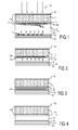
- Fig. 1 shows a structure of a radiation detector according to the prior art.
- the conversion arrangement 16 essentially consists of a first conversion layer 1 and a second conversion layer 2 are formed.
- the conversion layer 1 is with the Glass plate 2a with the photosensor arrangement 3 applied thereon using thin-film technology For example, connected in amorphous silicon technology via an adhesive layer 11.
- a reflection layer 9 is arranged, the light reflected upwards reflected back in the direction of the photosensor array.
- the glass support 4 carries the Glass plate 2a with the photosensor arrangement 3 applied thereon and the one located above it Conversion layer 1.
- Under the glass support 4 is an air layer 5 of about 10 mm high. Under this air layer 5, the lighting device 6 is included LEDs 7 (LED) arranged.
- the incident X-rays 15 pass through the reflection layer 9 and is in the conversion layer 1 in formed as a scintillator visible light converted.
- the visible light is in the photosensor arrangement 3 in electrical charge carriers converted, the readout electronics 12, under the lighting device 6 is arranged to be supplied.
- the readout electronics is through an X-ray shielding layer 13 is protected.
- the conversion layer 1 is over the glass plate 2a with the photosensor arrangement 2b arranged.
- the glass plate 2a and the photosensor arrangement 2b form the Conversion Layer 2
- These two conversion layers 1 and 2 are made by one load-bearing layer 8, for example made of acrylic. Titanium dioxide is added to the acrylic. It can also be any other suitable material for homogeneous light distribution with appropriate Stability can be used.
- Under this supporting layer 8 is the lighting device 6 arranged.
- a semiconductor layer made of CsI is evaporated. This eliminates the adhesive layer 11 between the first and second conversion layers 1, 2.
- FIG 3 shows a further embodiment of the invention.
- the conversion layer 1 arranged above the glass plate 2a with the photosensor arrangement 2b.
- a scattering film is located under the glass plate 2a with the photosensor arrangement 2b 14, which is applied directly to the surface of the lighting device 6.
- the lighting device 6 takes over the stabilizing function.
- FIG. 4 shows a radiation detector with a directly converting conversion arrangement 18.
- This comprises a conversion layer 19, for example made of amorphous selenium or made of PbO, a counterelectrode 20 and charge carrier sensors 17.
- the charge carrier sensors 17 comprise electrodes which, by means of a capacitance, charge carriers generated over time save so that they can be read out.
- the generation of load carriers in the Conversion layer 19 takes place in the electric field between counter electrode 20 and not pixel electrodes shown in the charge carrier sensors 17 instead.
- the conversion arrangement 18 is also arranged over the load-bearing layer 8, which in turn is over the Lighting device 6 is arranged.
- the supporting layer 8 distributes that from the lighting device emitted light homogeneously.
Abstract
Description
Die Erfindung betrifft einen Strahlungsdetektor zur Umwandlung von elektromagnetischer Strahlung in elektrische Ladungsträger. Des weiteren betrifft die Erfindung ein Röntgenuntersuchungsgerät mit einem derartigen Strahlungsdetektor und ein Verfahren zur Herstellung eines Strahlungsdetektors.The invention relates to a radiation detector for converting electromagnetic Radiation in electrical charge carriers. The invention further relates to an X-ray examination device with such a radiation detector and a method of manufacture a radiation detector.
Strahlungsdetektoren werden insbesondere in der Medizintechnik und dort in der Röntgenuntersuchungstechnik eingesetzt und dienen dazu, Strahlungsbilder eines Untersuchungsobjektes, in der Regel eines Patienten, im Rahmen einer zumeist medizinischen Untersuchung oder Therapie aufzunehmen. Mittels eines Bildaufnahmesystems, zu dem auch der Röntgenstrahlungsdetektor gehört, werden von der das Untersuchungsobjekt durchdringenden Röntgenstrahlung Bilder erzeugt, die bspw. auf einem Monitor ausgegeben werden. Die auf den Röntgenstrahlungsdetektor einfallende Röntgenstrahlung wird in einer Umwandlungsanordnung in elektrische Ladungsträger umgewandelt. Die in der Umwandlungsanordnung erzeugten elektrischen Ladungsträger werden in zugeordneten Kapazitäten gesammelt und von einer nachgeschalteten Ausleseelektronik ausgelesen.Radiation detectors are used particularly in medical technology and there in X-ray examination technology used and serve radiation images of an examination object, usually a patient, as part of a mostly medical To begin an examination or therapy. Using an image acquisition system to which also the X-ray detector is heard, of those penetrating the examination object X-ray radiation generates images that are output on a monitor, for example become. The X-radiation incident on the X-ray detector is in a Conversion arrangement converted into electrical charge carriers. The one in the conversion arrangement Electrical charge carriers are generated in assigned capacities collected and read out by a downstream readout electronics.
Ein Strahlungsdetektor ist generell derart aufgebaut, dass die elektromagnetische Strahlung auf eine Umwandlungsanordnung auftrifft. Je nach Ausgestaltung des Strahlungsdetektors wird die Strahlung in der Umwandlungsanordnung entweder in einer direkt konvertierenden Umwandlungsschicht in elektrische Ladungsträger umgewandelt, die dann ausgelesen werden, oder mittels zwei Umwandlungsschichten zuerst in sichtbares Licht und dann in einer darunter angeordneten zweiten Umwandlungsschicht, insbesondere einer Photosensorenanordnung, in elektrische Ladungsträger gewandelt und ausgelesen.A radiation detector is generally constructed in such a way that the electromagnetic radiation strikes a conversion arrangement. Depending on the design of the radiation detector the radiation in the conversion arrangement is either converted directly Conversion layer converted into electrical charge carriers, which are then read out or by means of two conversion layers first into visible light and then in one second conversion layer arranged underneath, in particular a photosensor arrangement, converted into electrical charge carriers and read out.
Bei Strahlungsdetektoren mit einer Umwandlungsanordnung, die zwei Umwandlungsschichten enthält, ist als erste Umwandlungsschicht eine Szintillatorschicht bspw. aus CsI:TI angeordnet. Unter dieser ersten Umwandlungsschicht, aus Sicht der einfallenden Strahlung, ist die zweite Umwandlungsschicht als Photosensorenanordnung ausgebildet. Die einzelnen Photosensoren detektieren die in sichtbares Licht umgewandelte Strahlung, die dann über die einzelnen Photosensoren pro Bildpixel ausgelesen werden. Die Umwandlung von Strahlung direkt in elektrische Ladungsträger in Strahlungsdetektoren mit einer Umwandlungsanordnung mit nur einer Umwandlungsschicht wird auch als Direktkonvertierung bezeichnet. Dabei ist die erste Umwandlungsschicht als direkt konvertierende Halbleiterschicht aus bspw. amorphem Selen ausgebildet. Strahlungsdetektoren mit direkter Umwandlung in nur einer Umwandlungsschicht können auch mittels einer PbO-Schicht realisiert sein, wobei die erzeugten Ladungsträger gespeichert und dann ausgelesen werden.In radiation detectors with a conversion arrangement, the two conversion layers contains, the first conversion layer is a scintillator layer, for example made of CsI: TI arranged. Under this first conversion layer, from the perspective of the incident radiation, the second conversion layer is designed as a photosensor arrangement. The single ones Photosensors detect the radiation converted into visible light, which is then transmitted through the individual photo sensors per image pixel can be read out. The conversion of radiation directly into electrical charge carriers in radiation detectors with a conversion arrangement with only one conversion layer is also called direct conversion. The first conversion layer is in the form of a directly converting semiconductor layer For example, amorphous selenium is formed. Radiation detectors with direct conversion to only a conversion layer can also be realized by means of a PbO layer, the generated charge carriers are stored and then read out.
Unter der oder den Umwandlungsschichten, in Abhängigkeit des Aufbaus des Strahlungsdetektors, ist eine Beleuchtungsvorrichtung angeordnet, die zum Rücksetzen der einzelnen Pixel der Photosensorenanordnung im Rahmen der Vorbereitung des Strahlendetektors für eine weitere zu erfolgende Bildaufnahme dient. Auch bei Strahlungsdetektoren, die nur eine Umwandlungsschicht zur direkten Konvertierung aufweisen, ist es zweckmäßig, durch einen Rücksetzlichtimpuls eine Ladungsträgerüberschwemmung hervorzurufen und dadurch das Abklingverhalten der Umwandlungsschicht positiv zu beeinflussen, so dass eine schnellere Röntgenbildaufnahmefolge möglich ist und/oder eine bessere Qualität ohne Bildartefakte erreicht wird.Under the conversion layer or layers, depending on the structure of the radiation detector, a lighting device is arranged to reset the individual Pixel of the photosensor arrangement as part of the preparation of the radiation detector for Another image to be taken is used. Even with radiation detectors that only have one Have conversion layer for direct conversion, it is appropriate to use a Reset light pulse cause a charge carrier flooding and thereby the Decay behavior of the conversion layer to influence positively, so that a faster X-ray image acquisition sequence is possible and / or better quality without image artifacts is achieved.
Diese bisher genannten Umwandlungsschichten werden von einem Substrat, bspw. aus Glas getragen.These previously mentioned conversion layers are made of a substrate, for example made of glass carried.
Es hat sich herausgestellt, dass die Photosensorenanordnung oder zweite Umwandlungsschicht ein langsames Abklingen zeigt, welches sich nachteilig auf aufeinanderfolgende Bildaufnahmen auswirkt. Dieses Abklingverhalten ist ganz besonders dann nachteilhaft, wenn pro Zeiteinheit viele Bilder akquiriert werden. Der Grund für dieses Abklingen liegt in physikalischen Vorgängen, die beim Einfallen von optischen Photonen in die Photosensoren ablaufen. Beim Einfallen eines Photons in das Halbleitermaterial der Photosensorenanordnung wird ein Elektron aus dem Valenzband in das Leitungsband angehoben und die so entstandene elektrische Ladung wird auf Elektroden der Halbleiterschicht, die eine Kapazität bilden, gespeichert. Da jedoch auf Grund von Verunreinigungen und Gitterfehlern in der Halbleiterschicht der Photosensorenanordnung sogenannte Traps oder Haftstellen vorhanden sind, bleiben manche Elektronen in der Halbleiterschicht hängen. Normalerweise werden die in den Traps befindlichen Ladungsträger in der Folgezeit thermisch emittiert und auf die Elektroden transferiert, wobei dies jedoch lange Zeit in Anspruch nehmen kann. Diese quasi thermische Emission, die auch dann stattfindet, wenn die Photosensorenanordnung bereits ausgelesen ist und ein zweites Bild aufgenommen wird, verursacht, dass in nachfolgend aufgenommenen Bildern sogenannte Nachbilder oder Bildartefakte des vorher aufgenommenen Bildes sichtbar sein können.It has been found that the photosensor array or second conversion layer a slow decay shows which adversely affects successive images effect. This decay behavior is particularly disadvantageous if pro Unit of time many images can be acquired. The reason for this decay is physical Processes that take place when optical photons enter the photosensors. When a photon falls into the semiconductor material of the photosensor arrangement an electron is lifted from the valence band into the conduction band and the resulting one electrical charge is applied to electrodes of the semiconductor layer, which form a capacitance saved. However, because of impurities and lattice defects in the semiconductor layer so-called traps or traps are present in the photosensor arrangement, some electrons get stuck in the semiconductor layer. Usually the in The charge carriers located in the traps subsequently emitted thermally and onto the electrodes transferred, but this can take a long time. This, so to speak thermal emission that takes place even when the photosensor arrangement already exists is read out and a second image is recorded, causing that in the subsequently recorded Images so-called afterimages or image artifacts of the previously recorded Image can be visible.
Um dieses Problem zu lösen, ist es bekannt, dass nach erfolgter Aufnahme eines Röntgenbildes die Photosensorenanordnung ausgelesen wird und anschließend wenigstens ein auf die zweite Umwandlungsschicht wirkender Lichtpuls mittels der Beleuchtungsvorrichtung abgegeben wird. Mittels des Lichtpulses wird die zweite Umwandlungsschicht mit Ladungsträgern überschwemmt und die Haftstellen in allen Pixeln gleichmäßig besetzt. Um eine möglichst effektive Besetzung der Haftstellen durch Ladungsträger zu erreichen, wird Licht einer bestimmten Wellenlänge von der Beleuchtungsvorrichtung mittels eines oder mehrerer separater Lichtimpulse in kurzer Abfolge emittiert. Voraussetzung für ein effektives Zurücksetzen ist jedoch, dass das Licht, welches von der Beleuchtungsvorrichtung ausgesendet wird, in Richtung der Photosensorenanordnung homogen verteilt wird.To solve this problem, it is known that after taking an X-ray the photosensor arrangement is read out and then at least one on the second conversion layer acting light pulse by means of the lighting device becomes. By means of the light pulse, the second conversion layer with charge carriers flooded and the traps in all pixels evenly occupied. To one Achieving the most effective possible way of filling the detention areas with charge carriers is light a certain wavelength from the lighting device by means of one or more separate light pulses are emitted in short succession. Requirement for an effective reset is, however, that the light emitted by the lighting device is distributed homogeneously in the direction of the photosensor arrangement.
In der DE 19914217 wird ein Röntgenstrahlendetektor beschrieben, bei dem eine Szintillatoranordnung über einer Pixelmatrix angeordnet ist und diese über einem Glasträger angeordnet sind, der die Szintillatoranordnung und die Pixelmatrix trägt. Unter dem Glasträger befindet sich eine Luftschicht und unter dieser Luftschicht ist die Lichtquelle oder Beleuchtungsvorrichtung angeordnet. Diese Luftschicht ist erforderlich, um eine räumliche Verteilung des von der Beleuchtungsvorrichtung abgestrahlten Lichts zu erreichen und um das Licht möglichst homogen zu verteilen. Die direkte Anordnung der Beleuchtungsvorrichtung unter dem Glasträger ohne eine entsprechende Luftschicht ist nachteilig, da dann die erforderliche homogene Lichtverteilung nicht erreicht wird und somit das Rücksetzen der Photosensorenanordnung und auch der Szintillator- oder Umwandlungsschicht nicht effektiv ist. Der Glasträger, der insbesondere zur Stabilisierung der auf ihm angeordneten Photosensorenanordnung und der Szintillator- oder Umwandlungsschicht dient, kann diese homogene Lichtverteilung nicht erbringen. Ein weiterer Nachteil des vorliegenden Detektors besteht in der erheblichen Höhe, welche durch die Glasträgerschicht und durch die Luftschicht entsteht.DE 19914217 describes an X-ray detector in which a scintillator arrangement is arranged above a pixel matrix and this is arranged above a glass substrate which carries the scintillator arrangement and the pixel matrix. Under the glass support there is an air layer and under this air layer is the light source or lighting device arranged. This layer of air is required to distribute space to achieve the light emitted by the lighting device and to To distribute light as homogeneously as possible. The direct arrangement of the lighting device under the glass support without an appropriate layer of air is disadvantageous because then the required homogeneous light distribution is not achieved and thus resetting the photosensor arrangement and the scintillator or conversion layer is also ineffective. The glass support, in particular for stabilizing the photosensor arrangement arranged on it and serves the scintillator or conversion layer, this can be homogeneous Do not provide light distribution. Another disadvantage of the present detector exists in the considerable height, which by the glass carrier layer and by the Air layer arises.
Aufgabe der Erfindung ist es deshalb, einen Strahlungsdetektor, ein Röntgenuntersuchungsgerät mit einem Strahlungsdetektor und ein Verfahren zur Herstellung eines Strahlungsdetektors anzugeben, bei denen bei gleichbleibend hoher Rücksetzanforderung eine niedrige Bauhöhe des Strahlungsdetektors ermöglicht wird.The object of the invention is therefore a radiation detector, an X-ray examination device with a radiation detector and a method for producing a radiation detector to be specified, for which a low reset requirement remains the same Height of the radiation detector is made possible.
Die Aufgabe wird mit einem Strahlungsdetektor zur Umwandlung von elektromagnetischer Strahlung in elektrische Ladungen gelöst, mit wenigstens einer Umwandlungsanordnung und einer Beleuchtungsvorrichtung und einer, wenigstens die Umwandlungsanordnung tragenden Schicht, wobei die tragende Schicht eine räumlich homogene Verteilung des von der Beleuchtungsvorrichtung ausgestrahlten Lichtes bewirkt.The task is done with a radiation detector for converting electromagnetic Radiation dissolved in electrical charges, with at least one conversion arrangement and a lighting device and one carrying at least the conversion arrangement Layer, the supporting layer having a spatially homogeneous distribution of that from the lighting device emitted light causes.
Der Erfindung liegt der Gedanke zugrunde, dass die Funktionen des die Umwandlungsschichten tragenden Glasträgers und der Luftschicht aus dem Stand der Technik vorteilhaft kombiniert werden können, was zu einer erheblichen Reduzierung der Bauhöhe mit weiteren, später detailliert erklärten Verbesserungen und vorteilhaften Wirkungen führt.The invention is based on the idea that the functions of the conversion layers supporting glass support and the air layer from the prior art advantageous can be combined, resulting in a significant reduction in overall height leads to further improvements and advantageous effects, which are explained in detail later.
Dazu wird vorgeschlagen, dass zwischen der Umwandlungsanordnung und der Beleuchtungsvorrichtung eine tragende Schicht angeordnet wird, die einerseits eine homogene Lichtverteilung vornimmt und andererseits eine ausreichende mechanische Stabilität aufweist, die über der tragenden Schicht angeordnete Umwandlungsanordnung aufzunehmen und stabil zu tragen. Die homogene Lichtverteilung ist zum effektiven Rücksetzen der Umwandlungsanordnung erforderlich und wird beim Stand der Technik durch die Luftschicht realisiert. Die homogene Lichtverteilung wird insbesondere dadurch erreicht, dass zwischen der Umwandlungsanordnung und der Beleuchtungsvorrichtung eine Kunststoffschicht, bspw. eine Acrylschicht angeordnet ist. Diese weist die erforderliche Lichtabsorption, Wärmeleitfähigkeit und auch mechanische Stabilität auf, um die darüber angeordneten Umwandlungsanordnungen zu tragen.For this purpose, it is proposed that between the conversion arrangement and the lighting device a load-bearing layer is arranged, on the one hand a homogeneous light distribution performs and on the other hand has sufficient mechanical stability, the Conversion arrangement arranged over the supporting layer and stable to wear. The homogeneous light distribution is for effectively resetting the conversion arrangement required and is the state of the art through the air layer realized. The homogeneous light distribution is achieved in particular by the fact that between the conversion arrangement and the lighting device a plastic layer, for example, an acrylic layer is arranged. This has the required light absorption, Thermal conductivity and also mechanical stability to the arranged above To carry conversion orders.
Die Beleuchtungsvorrichtung sendet das Rücksetzlicht insbesondere in Richtung der über ihr angeordneten Umwandlungsanordnung aus. Dabei ist es besonders effektiv, eine Wellenlänge zu wählen, die im Empfindlichkeitsbereich der Umwandlungsanordnung liegt. Hier ist es vorteilhaft, Licht mit einer Wellenlänge im Bereich von 300-900 nm auszuwählen.The lighting device sends the reset light in particular in the direction above it arranged conversion arrangement. It is particularly effective to use one wavelength to choose, which is in the sensitivity range of the conversion arrangement. Here it is advantageous to select light with a wavelength in the range of 300-900 nm.
In einer bevorzugten Ausführungsform der Erfindung sind in die tragende Schicht Kühlmittelräume eingebracht, denen eine Kühlflüssigkeit zuführbar ist, wodurch eine sehr effektive Wärmeabführung im Strahlungsdetektor erreichbar ist. Eine konstante Temperatur im Strahlungsdetektor wirkt sich vorteilhaft sowohl auf die Umwandlungsanordnung als auch auf die Auslesseelektronik aus. Durch eine geringere Temperatur erhöht sich bspw. die Empfindlichkeit der ersten Umwandlungsschicht, speziell bei CsI:Tl als Szintillatormaterial. Eine konstante Temperatur erhöht die Stabilität der Dunkelbilder.In a preferred embodiment of the invention, coolant spaces are in the supporting layer introduced, which can be supplied with a cooling liquid, making a very effective Heat dissipation in the radiation detector is achievable. A constant temperature in the Radiation detector has an advantageous effect both on the conversion arrangement and on the electronics. A lower temperature increases the sensitivity, for example the first conversion layer, especially with CsI: Tl as scintillator material. A constant temperature increases the stability of the dark images.
In einer weiteren vorteilhaften Ausgestaltung der Erfindung ist die Beleuchtungsvorrichtung mit einer Streufolie verbunden, so dass die Beleuchtungsvorrichtung die mechanische Stabilität oder den mechanischen Träger der darüber angeordneten Umwandlungsanordnung übernimmt. Dadurch lässt sich ein noch flacherer Strahlungsdetektor herstellen. Die Streufolie hat die Aufgabe, das von unten einfallende Rücksetzlicht homogen zu verteilen. Mittels der Folie kann vorteilhafterweise gegenüber dem Stand der Technik in dem flacheren Strahlungsdetektor die Wärme besser abtransportiert werden kann, so dass eine bisher benötigte Wasserkühlung entfallen kann.In a further advantageous embodiment of the invention, the lighting device connected with a scattering film, so that the lighting device mechanical stability or the mechanical support of the conversion arrangement arranged above takes over. This enables an even flatter radiation detector to be produced. The scatter foil has the task of distributing the reset light falling from below homogeneously. through the film can advantageously be compared to the prior art in the flatter radiation detector the heat can be better removed, so that a previously required Water cooling can be omitted.
Mittels der Acrylschicht oder der Streufolie kann vorteilhafterweise in dem Strahlungsdetektor die Wärme durch Wärmeleitung anstelle von Wärmestrahlung abtransportiert werden, so dass eine bisher benötigte Kühlung effizienter arbeiten oder ggfs. ganz entfallen kann.By means of the acrylic layer or the scattering foil can advantageously in the radiation detector the heat can be removed by heat conduction instead of heat radiation, so that a previously required cooling can work more efficiently or, if necessary, be completely eliminated.
In einer besonders vorteilhaften Ausgestaltung der Erfindung ist diese Acrylschicht direkt mit der Beleuchtungsvorrichtung vergossen, so dass die Beleuchtungsvorrichtung formschlüssig mit der tragenden Schicht verbunden ist.In a particularly advantageous embodiment of the invention, this acrylic layer is directly included potted the lighting device, so that the lighting device is positive is connected to the supporting layer.
Die Umwandlungsanordnung umfasst in einer ersten Ausführungsform zwei Umwandlungsschichten. Dabei wird die erste Umwandlungsschicht von einer Szintillatoranordnung gebildet. Diese erste Umwandlungsschicht wandelt die auf diese Umwandlungsschicht auftreffende Strahlung in sichtbares Licht. Unter dieser ersten Umwandlungsschicht ist eine zweite Umwandlungsschicht angeordnet. Diese Umwandlungsschicht wandelt das sichtbare Licht bspw. in einer Photosensorenanordnung in elektrische Ladungsträger.In a first embodiment, the conversion arrangement comprises two conversion layers. The first conversion layer is a scintillator arrangement educated. This first conversion layer converts the one striking this conversion layer Radiation in visible light. Under this first conversion layer is one second conversion layer arranged. This transformation layer changes the visible Light, for example, in a photosensor arrangement in electrical charge carriers.
In einer weiteren Ausführungsform der Erfindung umfasst die Umwandlungsanordnung nur eine direktkonvertierende Umwandlungsschicht. Diese wandelt die Röntgenstrahlung in elektrische Ladungsträger um, die über Elektroden ausgelesen werden.In a further embodiment of the invention, the conversion arrangement only comprises a directly converting conversion layer. This converts the X-rays into electrical charge carriers that are read out via electrodes.
Die Photosensorenanordnung ist in Dünnfilmtechnik auf einer Glasplatte aufgebracht. Nach dem Stand der Technik würde diese Glasplatte mit dem darunter liegenden Glasträger verklebt werden, wodurch eine zusätzliche Klebeschicht erforderlich wäre, in der bspw. Blasen auftreten können, die das von unten oder hinten einfallende Rücksetzlicht um bis zu 10 % abschwächen. An den Blasenrändern entstehen Inhomogenitäten, sogenannte Newtonringe, die ein gleichmäßiges Rücksetzen der Photosensorenanordnung, sowie eine räumlich aufgelöste Messung des Gaineffekts oder der Nichtlinearität der darüber angeordneten Photosensoren mit Hilfe des Rücksetzlichtes behindern.The photosensor arrangement is applied to a glass plate using thin film technology. To In the prior art, this glass plate would be glued to the glass carrier underneath be, which would require an additional adhesive layer, for example. Bubbles can occur that the reset light coming from below or behind by up to 10% weaken. Inhomogeneities, so-called Newton rings, which a uniform reset of the photosensor arrangement, as well as a spatially resolved Measurement of the Gaine effect or the non-linearity of the photosensors arranged above with the help of the reset light.
Ein weiterer Vorteil ergibt sich dadurch, dass die Schwingungen der Glasplatte durch die tragende Schicht, die bspw. aus Acryl gebildet ist, in Verbindung mit der Beleuchtungsvorrichtung gedämpft werden, wenn diese mechanisch an die Glasplatte, auf der die Photosensorenanordnung aufgebracht ist, angepresst wird, so dass sich Mikrophonieprobleme verringern.Another advantage results from the fact that the vibrations of the glass plate by the load-bearing Layer, for example made of acrylic, in connection with the lighting device are damped when these are mechanically attached to the glass plate on which the photosensor arrangement is applied, so that microphonic problems are reduced.
Sowohl eine direkt konvertierende Schicht aus PbO oder eine Szintillatoranordnung aus CsI:Tl kann auf die Glasplatte mit der in Dünnfilmtechnologie aufgebrachten Sensoren oder Elektroden aufgedampft werden.Both a directly converting layer made of PbO or a scintillator arrangement CsI: Tl can be applied to the glass plate using the sensors or thin film technology Electrodes are evaporated.
In einer vorteilhaften Ausführungsform wird auf der Rückseite der etwa 1 mm dicken Glasplatte mit der Photosensorenanordnung eine Acrylglasplatte von etwa 4 mm Dicke gelegt, die wiederum von der Beleuchtungsvorrichtung mechanisch gegen die Glasplatte mit der Photosensorenanordnung gedrückt wird. In an advantageous embodiment, the back is approximately 1 mm thick Glass plate with the photosensor arrangement an acrylic glass plate of about 4 mm thickness placed, which in turn mechanically against the glass plate with the lighting device the photosensor array is pressed.
In einer anderen vorteilhaften Ausführungsform der Erfindung wird die Beleuchtungsvorrichtung direkt nach der Bestückung mit bspw. LED's in eine flüssige Acrylmasse gepresst, so dass die Beleuchtungsvorrichtung mit der tragenden Schicht verbunden und direkt gekoppelt ist und eine plane Oberfläche erhält. Dadurch entstehen keine optischen Verluste durch eine zusätzliche Übergangsschicht zwischen Beleuchtungsvorrichtung und tragender Schicht. Die plane Oberfläche wird mechanisch an die Umwandlungsanordnung gepresst.In another advantageous embodiment of the invention, the lighting device directly after being fitted with e.g. LEDs into a liquid acrylic mass, see above that the lighting device is connected to the supporting layer and coupled directly and has a flat surface. As a result, there are no optical losses due to additional transition layer between the lighting device and the supporting layer. The flat surface is mechanically pressed against the conversion arrangement.
Vorteilhaft ist in beiden erwähnten Fällen eine Beimischung von bspw. Titandioxidpulver in geeigneter Konzentration zur tragenden Schicht, so dass die Verteilung des von den LED's oder von der Beleuchtungsvorrichtung emittierten Lichtes räumlich homogenisiert wird.In both of the cases mentioned, an admixture of, for example, titanium dioxide powder is advantageous suitable concentration to the supporting layer, so that the distribution of the LED's or spatially homogenized light emitted by the lighting device.
Zur besseren Wärmeabführung sowie zur Schwingungsdämpfung kann auch in dieser Ausführungsform die Beleuchtungsvorrichtung nach der Bestückung in Acrylmasse getaucht werden, um durch die plane Oberfläche einen großflächigen Kontakt zur Glasträgerplatte mit der Photosensorenanordnung zu gewährleisten. Hierbei wird dann aber kein Zusatz zur Lichtstreuung mehr benötigt.For better heat dissipation and vibration damping, this embodiment can also the lighting device is dipped in acrylic after assembly through the flat surface to make extensive contact with the glass support plate to ensure with the photosensor arrangement. Here, however, no addition to Light scattering needed more.
Die Aufgabe wird auch mit einem Röntgenuntersuchungsgerät gelöst, bei dem ein erfindungsgemäßer Röntgenstrahlungsdetektor einer Röntgenröhre gegenüber angeordnet wird und die von der Röntgenröhre ausgestrahlte Röntgenstrahlung einen Patienten oder ein zu untersuchendes Objekt passiert und auf den erfindungsgemäßen Röntgenstrahlungsdetektor trifft.The object is also achieved with an X-ray examination device in which an inventive device is used X-ray detector is arranged opposite an X-ray tube and the x-ray radiation emitted by the x-ray tube a patient or a examining object happens and on the X-ray detector according to the invention meets.
Die Aufgabe wird auch durch ein Verfahren zur Herstellung eines erfindungsgemäßen Strahlungsdetektors nach Anspruch 10 gelöst.The object is also achieved by a method for producing a radiation detector according to the invention solved according to claim 10.
Nachfolgend werden anhand der Figuren die Ausführungsbeispiele beschrieben.
- Fig.1
- zeigt einen schematischen Aufbau eines derzeitigen flachen dynamischen Röntgendetektors.
- Fig.2
- zeigt eine erste Ausführungsform des erfindungsgemäßen Strahlungsdetektors
- Fig.3
- zeigt eine zweite Ausführungsform des erfindungsgemäßen Strahlungsdetektors.
- Fig. 4
- zeigt einen Aufbau eines direkt konvertierenden Strahlungsdetektors
- Fig.1
- shows a schematic structure of a current flat dynamic X-ray detector.
- Fig.2
- shows a first embodiment of the radiation detector according to the invention
- Figure 3
- shows a second embodiment of the radiation detector according to the invention.
- Fig. 4
- shows a structure of a directly converting radiation detector
Fig. 1 zeigt einen Aufbau eines Strahlungsdetektors nach dem Stand der Technik. Dabei
wird die Umwandlungsanordnung 16 im wesentlichen aus einer ersten Umwandlungsschicht
1 und einer zweiten Umwandlungsschicht 2 gebildet. Die Umwandlungsschicht 1ist mit der
Glasplatte 2a mit der darauf in Dünnfilmtechnik aufgebrachten Photosensorenanordnung 3
bspw. in amorpher Siliziumtechnologie über eine Klebeschicht 11 verbunden. Über der Umwandlungsschicht
1 ist eine Reflexionsschicht 9 angeordnet, die nach oben reflektiertes Licht
zurück in die Richtung der Photosensorenanordnung reflektiert. Der Glasträger 4 trägt die
Glasplatte 2a mit der darauf aufgebrachten Photosensorenanordnung 3 und die darüber befindliche
Umwandlungsschicht 1. Unter dem Glasträger 4 ist eine Luftschicht 5 von etwa
10 mm Höhe angeordnet. Unter dieser Luftschicht 5 ist die Beleuchtungsvorrichtung 6 mit
Leuchtdioden 7 (LED) angeordnet. Die einfallende Röntgenstrahlung 15 passiert die Reflexionsschicht
9 und wird in der als Szintillator ausgebildeten Umwandlungsschicht 1 in
sichtbares Licht umgewandelt. Das sichtbare Licht wird in der Photosensorenanordnung 3 in
elektrische Ladungsträger umgewandelt, die einer Ausleseelektronik 12, die unter der Beleuchtungsvorrichtung
6 angeordnet ist, zugeführt werden. Die Ausleseelektronik ist durch
eine Röntgenstrahlen abschirmende Schicht 13 geschützt.Fig. 1 shows a structure of a radiation detector according to the prior art. there
the
In Fig.2 ist die Umwandlungsschicht 1 über der Glasplatte 2a mit der Photosensorenanordnung
2b angeordnet. Die Glasplatte 2a und die Photosensorenanordnung 2b bilden die
Umwandlungsschicht 2Diese beiden Umwandlungsschichten 1 und 2 werden von einer
tragenden Schicht 8, bspw. aus Acryl getragen. Dem Acryl ist Titandioxid beigemischt. Es
kann auch jedes andere geeignete Material zur homogenen Lichtverteilung mit entsprechender
Stabilität verwendet werden. Unter dieser tragenden Schicht 8 ist die Beleuchtungsvorrichtung
6 angeordnet. 2, the
Auf die Pixel mit den Photosensoren 2b und/oder den Kapazitäten zur Ladungsspeicherung
ist bspw. eine Halbleiterschicht aus CsI aufgedampft. Dadurch entfällt die Klebeschicht 11
zwischen der ersten und zweiten Umwandlungsschicht 1, 2.On the pixels with the
In Fig.3 ist eine weitere Ausführungsform der Erfindung dargestellt. Hierbei ist die Umwandlungsschicht
1 über der Glasplatte 2a mit der Photosensorenanordnung 2b angeordnet.
Unter der Glasplatte 2a mit der Photosensorenanordnung 2b befindet sich eine Streufolie
14, die direkt auf die Oberfläche der Beleuchtungsvorrichtung 6 aufgebracht ist. In dieser
Ausführungsform übernimmt die Beleuchtungsvorrichtung 6 die stabilisierende Funktion.3 shows a further embodiment of the invention. Here is the
Figur 4 zeigt einen Strahlungsdetektor mit einer direkt konvertierenden Umwandlungsanordnung
18. Diese umfasst eine Umwandlungsschicht 19, bspw. aus amorphem Selen oder
aus PbO, eine Gegenelektrode 20 und Ladungsträgersensoren 17. Die Ladungsträgersensoren
17umfassen Elektroden, die mittels einer Kapazität die erzeugten Ladungsträger über die Zeit
speichern, so dass diese ausgelesen werden können. Die Generation der Ladungsträger in der
Umwandlungsschicht 19 findet im elektrischen Feld zwischen Gegenelektrode 20 und nicht
dargestellten Pixelelektroden in den Ladungsträgersensoren 17 statt. Die Umwandlungsanordnung
18 ist auch hier über der tragenden Schicht 8 angeordnet, die wiederum über der
Beleuchtungsvorrichtung 6 angeordnet ist. Die tragende Schicht 8 verteilt das von der Beleuchtungsvorrichtung
ausgestrahlte Licht homogen.FIG. 4 shows a radiation detector with a directly converting
In den Figuren 2, 3, 4 ist deutlich sichtbar, dass der Strahlungsdetektor in einer wesentlich geringeren Höhe als nach dem Stand der Technik in Fig. 1 herstellbar ist.In Figures 2, 3, 4 it is clearly visible that the radiation detector is essential lower height than can be produced according to the prior art in FIG. 1.
Claims (11)
dadurch gekennzeichnet, dass die tragende Schicht (8) zwischen der Umwandlungsanordnung (16,18) und der Beleuchtungsvorrichtung (6) angeordnet ist und die Beleuchtungsvorrichtung (6) vorgesehen ist, Licht im Wellenlängenbereich von 300- 900 nm insbesondere in Richtung der Umwandlungsanordnung (16, 18) auszusenden.Radiation detector according to claim 1,
characterized in that the supporting layer (8) is arranged between the conversion arrangement (16, 18) and the lighting device (6) and the lighting device (6) is provided, light in the wavelength range of 300-900 nm, in particular in the direction of the conversion arrangement (16 , 18).
dadurch gekennzeichnet, dass die tragende Schicht (8) aus einem Material mit niedriger Lichtabsorption und/oder hoher Wärmeleitfähigkeit und /oder mechanischer Stabilität gebildet ist.Radiation detector according to claim 1,
characterized in that the supporting layer (8) is formed from a material with low light absorption and / or high thermal conductivity and / or mechanical stability.
dadurch gekennzeichnet, dass die tragende Schicht (8) formschlüssig mit der Beleuchtungsvorrichtung (6) verbunden ist. Radiation detector according to claim 1,
characterized in that the supporting layer (8) is positively connected to the lighting device (6).
dadurch gekennzeichnet, dass die tragende Schicht (8) Kühlmittelräume aufweist, denen von außen ein Kühlmittel zur Wärmeabfuhr zuführbar ist.Radiation detector according to claim 1,
characterized in that the load-bearing layer (8) has coolant spaces to which a coolant for heat dissipation can be supplied from the outside.
dadurch gekennzeichnet, dass die tragende Schicht (8) TiO2 enthält.Radiation detector according to claim 1,
characterized in that the supporting layer (8) contains TiO 2 .
dadurch gekennzeichnet, dass zwischen einer Umwandlungsanordnung (16,18) und einer Beleuchtungsvorrichtung (6) eine Streufolie (14) als Verteilungsschicht zur homogenen Lichtverteilung des von einer Beleuchtungsvorrichtung abgegebenen Lichtes angeordnet ist und die Beleuchtungsvorrichtung (6) die über ihr angeordneten Schichten (14) und Anordnungen (16,18) trägt.Radiation detector for converting electromagnetic radiation into electrical charge carriers
characterized in that between a conversion arrangement (16, 18) and a lighting device (6) a scattering film (14) is arranged as a distribution layer for homogeneous light distribution of the light emitted by a lighting device and the lighting device (6) the layers (14) arranged above it and arrangements (16, 18).
dadurch gekennzeichnet, dass die Umwandlungsanordnung (16) eine erste Umwandlungsschicht (1) zur Umwandlung von elektromagnetischer Strahlung in sichtbares Licht und eine zweite Umwandlungsschicht (2) zur Umwandlung von Licht in elektrische Ladungsträger umfasst, wobei die zweite Umwandlungsschicht (2) unter der ersten Umwandlungsschicht (1) aus Richtung der einfallenden elektromagnetischen Strahlung angeordnet ist. Radiation detector according to claims 1 to 7,
characterized in that the conversion arrangement (16) comprises a first conversion layer (1) for converting electromagnetic radiation into visible light and a second conversion layer (2) for converting light into electrical charge carriers, the second conversion layer (2) under the first conversion layer (1) is arranged from the direction of the incident electromagnetic radiation.
dadurch gekennzeichnet, dass die Umwandlungsanordnung (18) eine direkt konvertierende Umwandlungsschicht (19) zur Umwandlung von Röntgenstrahlung (15) in elektrische Ladungsträger, eine Gegenelektrode (20) und Ladungsträgersensoren (17) mit Auslese- und Speicherkomponenten umfasst.Radiation detector according to claims 1 to 7,
characterized in that the conversion arrangement (18) comprises a directly converting conversion layer (19) for converting x-ray radiation (15) into electrical charge carriers, a counter electrode (20) and charge carrier sensors (17) with readout and storage components.
Applications Claiming Priority (2)
| Application Number | Priority Date | Filing Date | Title |
|---|---|---|---|
| DE10132924A DE10132924A1 (en) | 2001-07-06 | 2001-07-06 | Flat dynamic radiation detector |
| DE10132924 | 2001-07-06 |
Publications (1)
| Publication Number | Publication Date |
|---|---|
| EP1273932A1 true EP1273932A1 (en) | 2003-01-08 |
Family
ID=7690920
Family Applications (1)
| Application Number | Title | Priority Date | Filing Date |
|---|---|---|---|
| EP02100781A Withdrawn EP1273932A1 (en) | 2001-07-06 | 2002-07-04 | Flat dynamic radiation detector having an illumination device |
Country Status (4)
| Country | Link |
|---|---|
| US (1) | US6989539B2 (en) |
| EP (1) | EP1273932A1 (en) |
| JP (1) | JP2003107162A (en) |
| DE (1) | DE10132924A1 (en) |
Cited By (1)
| Publication number | Priority date | Publication date | Assignee | Title |
|---|---|---|---|---|
| CN110892291A (en) * | 2017-07-26 | 2020-03-17 | 深圳帧观德芯科技有限公司 | X-ray detector |
Families Citing this family (12)
| Publication number | Priority date | Publication date | Assignee | Title |
|---|---|---|---|---|
| JP2005539232A (en) * | 2002-09-18 | 2005-12-22 | コーニンクレッカ フィリップス エレクトロニクス エヌ ヴィ | X-ray detector having a plurality of detector units |
| JP2007527987A (en) * | 2003-04-24 | 2007-10-04 | コーニンクレッカ フィリップス エレクトロニクス エヌ ヴィ | X-ray detector element |
| JP4254602B2 (en) * | 2004-04-19 | 2009-04-15 | 株式会社島津製作所 | Two-dimensional radiation detector |
| DE102005037898B3 (en) * | 2005-08-10 | 2007-04-12 | Siemens Ag | Solid state detector or method for resetting residual charges by illumination in a solid-state detector |
| JP4921180B2 (en) * | 2006-01-25 | 2012-04-25 | キヤノン株式会社 | Radiation detection apparatus and radiation imaging system |
| DE102006010004B4 (en) * | 2006-03-03 | 2016-10-13 | Siemens Healthcare Gmbh | X-ray detector |
| CN101669041B (en) * | 2007-04-23 | 2012-11-28 | 皇家飞利浦电子股份有限公司 | Detector with a partially transparent scintillator substrate |
| JP4834614B2 (en) * | 2007-06-12 | 2011-12-14 | キヤノン株式会社 | Radiation detection apparatus and radiation imaging system |
| US8772728B2 (en) * | 2010-12-31 | 2014-07-08 | Carestream Health, Inc. | Apparatus and methods for high performance radiographic imaging array including reflective capability |
| WO2014072939A1 (en) * | 2012-11-09 | 2014-05-15 | Koninklijke Philips N.V. | Sub-band infra-red irradiation for detector crystals |
| US9482762B2 (en) | 2014-08-28 | 2016-11-01 | Infineon Technologies Ag | Gamma ray detector and method of detecting gamma rays |
| DE102016210935B4 (en) * | 2016-06-20 | 2020-07-09 | Siemens Healthcare Gmbh | X-ray detector with a non-transparent intermediate layer |
Citations (5)
| Publication number | Priority date | Publication date | Assignee | Title |
|---|---|---|---|---|
| US4945243A (en) * | 1988-02-26 | 1990-07-31 | Thomson-Csf | Matrix of photosensitive elements and radiation detector including such a matrix, especially double-energy X-ray detector |
| US4980553A (en) * | 1988-05-03 | 1990-12-25 | Thomson-Csf | Radiological image detector |
| DE4420603C1 (en) * | 1994-06-13 | 1995-06-22 | Siemens Ag | X=ray image detector with erasure light source |
| US5563421A (en) * | 1995-06-07 | 1996-10-08 | Sterling Diagnostic Imaging, Inc. | Apparatus and method for eliminating residual charges in an image capture panel |
| DE19914217A1 (en) * | 1999-03-29 | 2000-10-05 | Siemens Ag | Operating X-ray beam detector includes forming light pulse on scintillator layer using light source |
Family Cites Families (21)
| Publication number | Priority date | Publication date | Assignee | Title |
|---|---|---|---|---|
| US3594583A (en) * | 1966-08-22 | 1971-07-20 | Sheldon Edward E | Electro-optical devices for detecting images of invisible radiations using interaction of light beams |
| US5493122A (en) * | 1994-02-04 | 1996-02-20 | Nucleonics Development Company | Energy resolving x-ray detector |
| US5636299A (en) * | 1994-12-28 | 1997-06-03 | Lockheed Missiles & Space Company, Inc. | Hybrid luminescent device and method for imaging penetrating radiation |
| DE19524856A1 (en) * | 1995-07-07 | 1997-01-09 | Siemens Ag | X-ray imaging system |
| US6362484B1 (en) * | 1995-07-14 | 2002-03-26 | Imec Vzw | Imager or particle or radiation detector and method of manufacturing the same |
| US5652430A (en) * | 1996-05-03 | 1997-07-29 | Sterling Diagnostic Imaging, Inc. | Direct radiographic imaging panel |
| US6502984B2 (en) * | 1997-01-17 | 2003-01-07 | Canon Kabushiki Kaisha | Radiographic apparatus |
| US5848122A (en) * | 1997-03-25 | 1998-12-08 | Advanced Technology Materials, Inc. | Apparatus for rapid in-situ X-ray stress measurement during thermal cycling of semiconductor wafers |
| US5956382A (en) * | 1997-09-25 | 1999-09-21 | Eliezer Wiener-Avnear, Doing Business As Laser Electro Optic Application Technology Comp. | X-ray imaging array detector and laser micro-milling method for fabricating array |
| JPH11307756A (en) * | 1998-02-20 | 1999-11-05 | Canon Inc | Photoelectric converter and radiation beam reader |
| DE19808936A1 (en) * | 1998-03-03 | 1999-09-16 | Aventis Res & Tech Gmbh & Co | Photodetector and its use |
| JP4011734B2 (en) * | 1998-06-02 | 2007-11-21 | キヤノン株式会社 | Two-dimensional optical sensor, radiation detection apparatus and radiation diagnostic system using the same |
| US6194727B1 (en) * | 1998-07-06 | 2001-02-27 | Direct Radiography Corp. | Direct radiographic imaging panel having a dielectric layer with an adjusted time constant |
| FR2782388B1 (en) * | 1998-08-11 | 2000-11-03 | Trixell Sas | SOLID STATE RADIATION DETECTOR WITH INCREASED LIFE |
| US6642650B1 (en) * | 1998-11-10 | 2003-11-04 | Agfa-Gevaert | Refusable personal monitoring device |
| US6326625B1 (en) * | 1999-01-20 | 2001-12-04 | Edge Medical Devices Ltd. | X-ray imaging system |
| US6440769B2 (en) * | 1999-11-26 | 2002-08-27 | The Trustees Of Princeton University | Photovoltaic device with optical concentrator and method of making the same |
| DE10034575A1 (en) * | 2000-07-14 | 2002-01-24 | Philips Corp Intellectual Pty | X-ray detector with improved light output |
| FR2812089B1 (en) * | 2000-07-21 | 2007-11-30 | Trixell Sas | RADIATION DETECTOR WITH INCREASED LIFETIME |
| US6717150B2 (en) * | 2000-12-12 | 2004-04-06 | Ge Medical Systems Global Technology Company, Llc | Solid-state CT detector modules with improved scintillator/diode coupling |
| US6510195B1 (en) * | 2001-07-18 | 2003-01-21 | Koninklijke Philips Electronics, N.V. | Solid state x-radiation detector modules and mosaics thereof, and an imaging method and apparatus employing the same |
-
2001
- 2001-07-06 DE DE10132924A patent/DE10132924A1/en not_active Withdrawn
-
2002
- 2002-07-04 JP JP2002195674A patent/JP2003107162A/en not_active Withdrawn
- 2002-07-04 EP EP02100781A patent/EP1273932A1/en not_active Withdrawn
- 2002-07-08 US US10/189,960 patent/US6989539B2/en not_active Expired - Fee Related
Patent Citations (5)
| Publication number | Priority date | Publication date | Assignee | Title |
|---|---|---|---|---|
| US4945243A (en) * | 1988-02-26 | 1990-07-31 | Thomson-Csf | Matrix of photosensitive elements and radiation detector including such a matrix, especially double-energy X-ray detector |
| US4980553A (en) * | 1988-05-03 | 1990-12-25 | Thomson-Csf | Radiological image detector |
| DE4420603C1 (en) * | 1994-06-13 | 1995-06-22 | Siemens Ag | X=ray image detector with erasure light source |
| US5563421A (en) * | 1995-06-07 | 1996-10-08 | Sterling Diagnostic Imaging, Inc. | Apparatus and method for eliminating residual charges in an image capture panel |
| DE19914217A1 (en) * | 1999-03-29 | 2000-10-05 | Siemens Ag | Operating X-ray beam detector includes forming light pulse on scintillator layer using light source |
Cited By (2)
| Publication number | Priority date | Publication date | Assignee | Title |
|---|---|---|---|---|
| CN110892291A (en) * | 2017-07-26 | 2020-03-17 | 深圳帧观德芯科技有限公司 | X-ray detector |
| CN110892291B (en) * | 2017-07-26 | 2024-03-12 | 深圳帧观德芯科技有限公司 | X-ray detector |
Also Published As
| Publication number | Publication date |
|---|---|
| DE10132924A1 (en) | 2003-01-16 |
| JP2003107162A (en) | 2003-04-09 |
| US20030020019A1 (en) | 2003-01-30 |
| US6989539B2 (en) | 2006-01-24 |
Similar Documents
| Publication | Publication Date | Title |
|---|---|---|
| DE69534284T2 (en) | SEMICONDUCTOR GAMMA RADIATION CAMERA AND MEDICAL IMAGING SYSTEM | |
| DE69926769T2 (en) | SINTINATOR PANEL, RADIATION IMAGE SENSOR AND METHOD FOR THE PRODUCTION THEREOF | |
| DE69836190T2 (en) | HIGH RESOLUTION RADIATION IMAGING SYSTEM | |
| EP2453263B1 (en) | Hybrid organic photodiodes | |
| DE69730687T2 (en) | APPARATUS AND METHOD FOR IMAGING X-RAY RAYS WITH A FLAT IMAGE RECORDING UNIT OF AMORPHIC SILICON | |
| US8338790B2 (en) | Radiation-sensitive detector with a scintillator in a composite resin | |
| DE112014003002T5 (en) | X-ray image converter with CMOS sensor embedded in a TFT panel | |
| EP1273932A1 (en) | Flat dynamic radiation detector having an illumination device | |
| DE102008016008A1 (en) | Photon-counting CT detector using a solid-state photomultiplier and scintillator | |
| DE102005049228B4 (en) | Detector with an array of photodiodes | |
| DE10244176A1 (en) | X-ray detector for use in digital imaging, especially CT applications, has a multi-layer structure with interleaved support, fluorescing and photo-sensor layers to permit energy-resolved radiation detection | |
| DE69927522T2 (en) | RADIATION IMAGE SENSOR AND METHOD FOR THE PRODUCTION THEREOF | |
| DE102010004890A1 (en) | Photodiode array, radiation detector and method for producing such a photodiode array and such a radiation detector | |
| DE112015004713T5 (en) | Photon counting detector | |
| DE102006033716A1 (en) | X-ray diagnosis apparatus, with digital imaging, has a dosage measurement sensor using part of the scintillating light with a matrix of detection sensors | |
| DE102005056048B4 (en) | Flat panel detector | |
| DE2038607A1 (en) | Ray imaging device | |
| DE102006042484A1 (en) | Radiation detector e.g. flat image detector, for e.g. X-ray radiography, has lens array with micro lenses arranged between scintillator plate and photo sensor, where lenses are partially designed as convex lenses | |
| DE4410269A1 (en) | X-ray image recording tube | |
| DE69832602T2 (en) | ILLUSTRATING SOLID-BODY DETECTOR IS EXPOSED TO IONIZING RADIATION AND HAS A MEASURING DEVICE | |
| DE102011004936A1 (en) | X-ray detector and medical X-ray device | |
| DE102011080892B3 (en) | Direct conversion type x-ray detector for use in computed tomography system, has scintillation layer that is arranged on x-ray radiation facing side of semiconductor, and is made of material with specific decay time | |
| EP0143205B1 (en) | Position resolving, light-sensitive diode arrangement and method for its production | |
| DE102009060315A1 (en) | Counting x-ray detector | |
| DE102011077056A1 (en) | Radiation detector and imaging system |
Legal Events
| Date | Code | Title | Description |
|---|---|---|---|
| PUAI | Public reference made under article 153(3) epc to a published international application that has entered the european phase |
Free format text: ORIGINAL CODE: 0009012 |
|
| AK | Designated contracting states |
Kind code of ref document: A1 Designated state(s): AT BE BG CH CY CZ DE DK EE ES FI FR GB GR IE IT LI LU MC NL PT SE SK TR |
|
| AX | Request for extension of the european patent |
Free format text: AL;LT;LV;MK;RO;SI |
|
| RAP1 | Party data changed (applicant data changed or rights of an application transferred) |
Owner name: PHILIPS INTELLECTUAL PROPERTY & STANDARDS GMBH Owner name: KONINKLIJKE PHILIPS ELECTRONICS N.V. |
|
| 17P | Request for examination filed |
Effective date: 20030708 |
|
| AKX | Designation fees paid |
Designated state(s): DE FR GB NL |
|
| 17Q | First examination report despatched |
Effective date: 20091111 |
|
| STAA | Information on the status of an ep patent application or granted ep patent |
Free format text: STATUS: THE APPLICATION IS DEEMED TO BE WITHDRAWN |
|
| 18D | Application deemed to be withdrawn |
Effective date: 20100323 |