EP1274260A2 - Matrix switch device with high isolation, small size, and low manufacturing cost - Google Patents
Matrix switch device with high isolation, small size, and low manufacturing cost Download PDFInfo
- Publication number
- EP1274260A2 EP1274260A2 EP02015017A EP02015017A EP1274260A2 EP 1274260 A2 EP1274260 A2 EP 1274260A2 EP 02015017 A EP02015017 A EP 02015017A EP 02015017 A EP02015017 A EP 02015017A EP 1274260 A2 EP1274260 A2 EP 1274260A2
- Authority
- EP
- European Patent Office
- Prior art keywords
- matrix switch
- input terminals
- matrix
- external wiring
- spdt
- Prior art date
- Legal status (The legal status is an assumption and is not a legal conclusion. Google has not performed a legal analysis and makes no representation as to the accuracy of the status listed.)
- Granted
Links
Images


Classifications
-
- H—ELECTRICITY
- H04—ELECTRIC COMMUNICATION TECHNIQUE
- H04Q—SELECTING
- H04Q3/00—Selecting arrangements
- H04Q3/42—Circuit arrangements for indirect selecting controlled by common circuits, e.g. register controller, marker
- H04Q3/52—Circuit arrangements for indirect selecting controlled by common circuits, e.g. register controller, marker using static devices in switching stages, e.g. electronic switching arrangements
- H04Q3/521—Circuit arrangements for indirect selecting controlled by common circuits, e.g. register controller, marker using static devices in switching stages, e.g. electronic switching arrangements using semiconductors in the switching stages
Landscapes
- Engineering & Computer Science (AREA)
- Computer Networks & Wireless Communication (AREA)
- Electronic Switches (AREA)
- Waveguide Switches, Polarizers, And Phase Shifters (AREA)
Abstract
Description
- The present invention relates to a matrix switch device, which is mounted in a home receiving antenna of a digital satellite broadcasting (DSB) system and is suitable for switching input signals from a plurality of satellites.
- Multi-satellite systems and multi-channel systems are increasingly used for satellite broadcasting. Therefore, as a low noise block (LNB), a matrix switch device for switching input signals from the plurality of satellites and especially a matrix switch integrated circuit, which is a matrix switch device formed as a semiconductor integrated circuit, are highly demanded. Incidentally, the LNB is a BS/CS receiving front-end mounted in the home receiving antenna of the DBS system. To this end, a 2×2 matrix switch integrated circuit, which is a matrix switch device having two input terminals and two output terminals, is developed.
- Hitherto, optimization of the size of the elements of the 2×2 matrix switch integrated circuit has been performed for improving ON/OFF characteristics of the switch thereof. Optimization of wiring layout on the integrated circuit chip thereof has also been performed for reducing signal interference caused by dense wiring for inter-connecting the switches thereof. Further, optimization of the package thereof for mounting the 2×2 matrix switch integrated circuit therein, and optimization of mounting and assembly methods have also been performed for achieving high isolation characteristics.
- On the other hand, a matrix switch device is demanded, the matrix switch device being capable of receiving broadcasting signals from the plurality of satellites and switching between multiple channels, the number of channels being more than previously achieved. For example, the recently used DBS system, which receives broadcasting signals from two satellites, requires a 4×2 matrix switch device for receiving and switching horizontally and vertically polarized wave signals from the satellites. An exemplary 4×2 matrix switch device comprises first and second input terminals to which the horizontally and vertically polarized wave signals are input from one of the satellites, and comprises third and fourth input terminals to which the horizontally and vertically polarized wave signals are input from another satellite. A very high isolation characteristic is required between the first and second input terminals and between the third and fourth input terminals.
- The above-described 4×2 matrix switch device further comprises two 2×2 matrix switch integrated circuits which achieve high isolation, a plurality of PIN diodes, and the mounting board. The 2×2 matrix switch integrated circuits and the PIN diodes are mounted on the mounting board and are inter-connected by wiring lines on the mounting board. Other matrix switch integrated circuits and PIN diodes are disposed ' between the first and second input terminals and between the third and fourth input terminals where high isolation is required, and the first to fourth input terminals are inter-connected by external wiring lines. Therefore, signal interference in the wiring lines on the board is reduced and the high isolation characteristic is achieved.
- The 4×2 matrix switch device each comprises two PIN diodes on four circuit wiring lines, that is, eight PIN diodes in total. The PIN diodes, however, requires high isolation for signals transmitted in the reverse direction (from the output direction to the input direction). Therefore, the PIN diodes must be disposed in series. Accordingly, the number of parts of the existing 4×2 matrix switch device is at least ten. This large number of parts results in a mounting board with an increased area and an increased number of assembly-adjusting procedures. Accordingly, the cost of the 4×2 matrix switch device also increases.
- In view of the above, a low-
cost 4×2 matrix switch integrated circuit should be developed. This 4×2 matrix switch integrated circuit comprises twelve switches for example. The control voltage of the switches is set to a suitable level so that the first and second output terminals thereof can separately select and switch the input signals. - As in the case of the 2×2 matrix switch integrated circuit, optimization of the size of the elements of the 4×2 matrix switch integrated circuit is performed for increasing the ON/OFF characteristics of the switches. Optimization of the wiring layout on the IC chip thereof is also performed for reducing signal interference caused by dense wiring for inter-connecting the switches. Further, optimization of the package thereof for mounting the 4×2 matrix switch integrated circuit therein, and optimization of mounting and assembly methods are also performed for increasing the isolation characteristic.
- However, since the number of switches of the 4×2 matrix switch integrated circuit is increased, the amount of wiring lines for inter-connecting the switches becomes twice as much as that of the 2×2 matrix switch integrated circuit. Further, the wiring line on the integrated circuit chip becomes complicated due to the increased number of D lines for the switches. Subsequently, the distance between the switches on the integrated circuit chip decreases, and the density and crossovers of the signal wiring lines increase more than in the case of the 2×2 matrix switch integrated circuit. Since the signal interference is not sufficiently reduced, the isolation of the 4×2 matrix switch integrated circuit does not easily increase.
- Keeping sufficient distances between the switches (FET) and the signal wiring line is effective for decreasing the signal interference. However, this method may result in a semiconductor integrated circuit chip with an increased size and an increased cost of the switches. In such a case, a large-sized package will be required according to the increased size of the semiconductor integrated circuit chip. However, manufacturing a new production line for such packages will significantly increase the cost of the switches.
- Accordingly, the object of the present invention is to provide a matrix switch device comprising a semiconductor integrated circuit chip functioning as a satellite reception unit having high isolation between the terminals thereof and that is small and susceptible of low cost of manufacture because of the reduced number of elements thereof.
- A matrix switch device according to a first aspect of the present invention comprises a semiconductor integrated circuit chip. The semiconductor integrated circuit chip comprises a 2×2 matrix switch having two input terminals and two output terminals, and an SPDT (Single Pole Double Throw) switch at a stage subsequent to the 2×2 matrix switch, which has two input terminals and one output terminal. Electrical connection is performed between one of the output terminals of the 2×2 matrix switch and one of the input terminals of the SPDT switch. The two input terminals and the other of said output terminals of the 2×2 matrix switch, and the other input terminal and the output terminal of the SPDT switch are led out of the semiconductor integrated circuit chip.
- A matrix switch device according to a second aspect of the present invention comprises a semiconductor integrated circuit chip. The semiconductor integrated circuit chip comprises a 2×2 matrix switch having two input terminals and two output terminals, and an SPDT switch at a stage subsequent to the 2×2 matrix switch, which has two input terminals and one output terminal. The input terminals and the output terminals of the 2×2 matrix switch, and the input terminals and the output terminal of the SPDT switch are led out of the semiconductor integrated circuit chip.
- A 4×2 matrix switch device according to a third aspect of the present invention comprises a first matrix switch unit comprising the above-described matrix switch device packaged in a first package and a second matrix switch unit comprising the matrix switch device packaged in a second package. The 4×2 matrix switch device further comprises a first external wiring line and a second external wiring line. Electrical connection is performed between the other of said output terminals of the 2×2 matrix switch of the first matrix switch unit and the other of said input terminals of the SPDT switch of the second matrix switch unit via the first external wiring line outside the first and second packages. Electrical connection is also performed between the other of said output terminals of the 2×2 matrix switch of the second matrix switch unit and the other of said input terminals of the SPDT switch of the first matrix switch unit via the second external wiring line outside the first and second packages.
- The other objects of this invention will become clear as the description proceeds.
-
- Fig. 1A is a circuit diagram of a switch of a related matrix switch device, Fig. 1B schematically shows the switch;
- Fig. 2A is a circuit diagram of the related matrix switch device, Fig. 2B is schematically shows the function of the related matrix switch device;
- Fig. 3 schematically shows the configuration of a related matrix switch device;
- Fig. 4A is a circuit diagram of a related 4×2 matrix switch integrated circuit, Fig. 4B schematically shows the related 4×2 matrix switch integrated circuit;
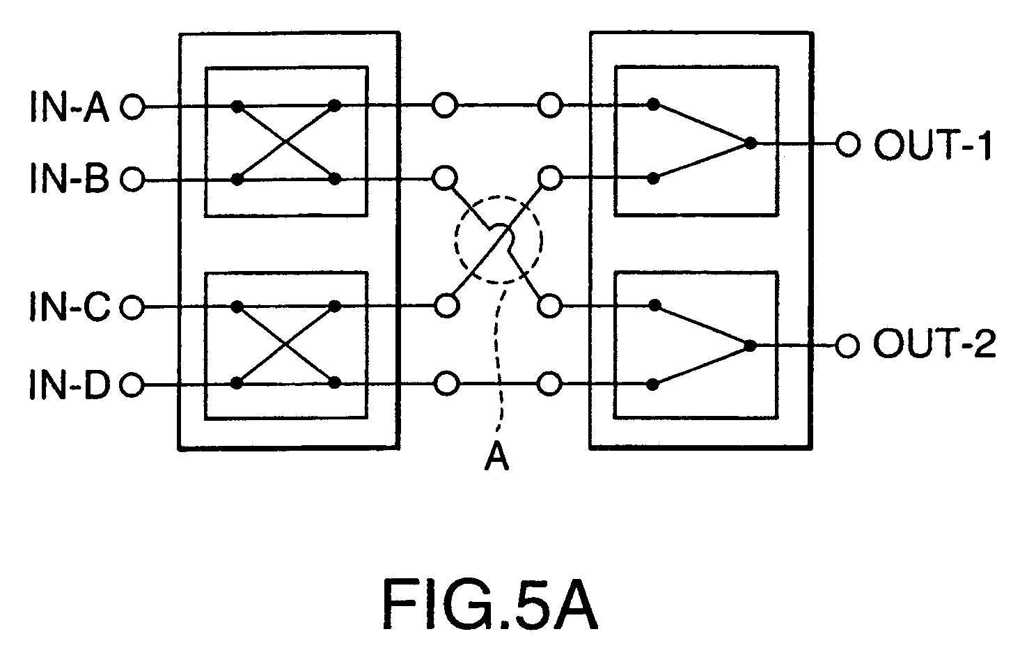
- Fig. 5A shows a 4×2 matrix switch integrated circuit comprising two semiconductor integrated circuits, Fig. 5B shows another 4×2 matrix switch integrated circuit comprising two semiconductor integrated circuits;
- Fig. 6A is a circuit diagram of a single-pole double-throw (SPDT) switch, Fig. 6B schematically shows the SPDT switch;
- Fig. 7 schematically shows the configuration of a matrix switch integrated circuit device according to a first embodiment of the present invention;
- Fig. 8 schematically shows the configuration of a matrix switch device according to a second embodiment of the present invention.
- Fig. 9 schematically shows the configuration of a matrix switch device according to a third embodiment of the present invention;
- Fig. 10 schematically shows the configuration of a matrix switch device according to a fourth embodiment of the present invention;
- Fig. 11 schematically shows the configuration of a matrix switch device according to a fifth embodiment of the present invention;
- Fig. 12 is a schematic perspective view of a matrix switch device according to a sixth embodiment of the present invention;
- Fig. 13A is schematic perspective view of another matrix switch device, Fig. 13B is a schematic sectional view of the matrix switch device shown in Fig. 13A; and
- Fig. 14 is a schematic sectional view of a matrix switch device according to an eighth embodiment of the present invention.
-
- In order to facilitate an understanding of the present invention, description will at first be made about the related matrix switch related to the present invention with reference to the drawings.
- First, the configuration of a related 2×2 matrix switch integrated
circuit 100 will be described with reference to Figs. 1A, 1B, 2A, and 2B, As shown in Fig. 2A, the 2×2 matrix switch integratedcircuit 100 comprises two input terminals IN-A and IN-B, fourswitches 100a, and two output terminals OUT1 and OUT2. Fig. 1A shows the configuration of theswitch 100a, which comprises an input terminal, an output terminal, two field effect transistors (FET) Tr1 and Tr2, and a capacitor. The transistor Tr1, which has an ON characteristic, has one end connected to the input terminal and another end connected to the output terminal. The transistor Tr2, which has an OFF characteristic, has one end connected to the input terminal and another end RF-grounded via the capacitor. When one of these transistors Tr1 and Tr2 is operated and the other is not operated, ON/OFF operation is performed. Fig. 1B is a schematic diagram of theswitch 100a. - Fig. 2B is a conceptual illustration of the 2×2 matrix SW-
IC 100. When the control voltage of theswitch 100a is set to a suitable level, the output terminals OUT1 and OUT2 can separately select and switch the input signals. - Hitherto, optimization of the size of the elements of the 2×2 matrix switch Integrated
circuit 100 is performed for improving the ON/OFF characteristics of theswitch 100a. Optimizations of the wiring layout on the integrated circuit chip thereof are also performed for reducing signal interference caused by dense wiring for inter-connecting theswitches 100a. Further, optimization of the package for mounting the 2×2 matrix SW-IC 100 therein, and optimization of the mounting and assembly methods are also performed for achieving high isolation characteristics. - On the other hand, a matrix switch device, which receives a broadcasting signal from the plurality of satellites and which can switch between multiple channels, the number of channels being more than previously achieved, is demanded. Fig. 3 shows the configuration of an exemplary 4×2 matrix switch:
device 610, which comprises two 2×2 matrix switch integratedcircuits 100, four PIN diodes D1, four PIN diodes D2, input terminals IN-A, IN-B, IN-C, and IN-D, and output terminals OUT1 and OUT2. The recently used DBS system, which receives broadcasting signals from first and second satellites for example, requires such a 4×2 matrix switch device for receiving and switching horizontally and vertically polarized wave signals from the satellites. High isolation is required between the input terminals IN-A and IN-B where horizontally and vertically polarized wave signals are input from the first satellite and between the input terminals IN-C and IN-D where horizontally and vertically polarized wave signals are input from the second satellite, for reducing the interference between the signals from the first and second satellites. - More specifically, two 2×2 matrix switch integrated
circuits 100, which achieve high isolation, and the plurality of PIN diodes D1 and D2 are mounted on a mounting board and are inter-connected by wiring line on the mounting board. These matrix switch integrated circuits and the PIN diodes are disposed between the input terminals IN-A and IN-B and between the input terminals IN-C and the IN-D, where high isolation is required. The input terminals IN-A to IN-D are connected by external wiring lines. Therefore, signal interference in the wiring lines on the board is reduced and the high isolation is achieved. - The 4×2
matrix switch device 610 comprises one of the PIN diodes D1 and one of the PIN diodes D2 on the wiring lines thereof. The PIN diodes D1 and D2, however, require high isolation for signals transmitted in the reverse direction (from the output direction to the input direction). Therefore, the PIN diodes D1 and D2 must be disposed in series. Accordingly, the 4×2matrix switch device 610 has at least ten parts. This large number of parts results in the mounting board with an increased area and an increased number of assembly-adjusting procedures. Accordingly, the cost of the 4×2matrix switch device 610 also increases. - In view of the above, a low-
cost 4×2 matrix switch integrated circuit should be developed. Fig. 4A illustrates the configuration of an exemplary 4×2 matrix switch integrated circuit comprising twelveswitches 100a. Fig. 4B is a conceptual illustration of the 4×2 matrix switch integrated circuit. The control voltage of theswitches 100a is set to a suitable level so that the output terminals OUT-1 and OUT-2 can separately select and switch input signals. - As in the case of the 2×2 matrix switch integrated
circuit 100, optimization of the size of the elements of the 4×2 matrix switch integrated circuit is performed for increasing the ON/OFF characteristics of theswitches 100a. Optimization of the wiring layout on the IC chip thereof is also performed for reducing signal interference caused by dense wiring for inter-connecting the switches. Further, optimization of the package thereof for mounting the 4×2 matrix switch integrated circuit therein, and optimization of the mounting and assembly methods is also performed for increasing the isolation characteristic. - However, since the number of switches of the 4×2 matrix switch integrated circuit is increased, the amount of wiring lines for inter-connecting the
switches 100a becomes twice as much as that of the 2 ×2 matrix switch integratedcircuit 100. Further, the wiring on the integrated circuit chip becomes complicated due to the increased number of D lines for theswitches 100a. Subsequently, the distance between the switches on the integrated circuit chip decreases, and the density and crossovers of the signal wiring lines increase more than in the case of the 2×2 matrix switch integratedcircuit 100. Since the signal interference is not sufficiently reduced, the isolation of the 4×2 matrix switch integrated circuit does not easily increase. - Next, a matrix switch device according to embodiments of the present invention will now be described with reference to Figs. 5A to 14.
- As has been described, achieving a high isolation characteristic at low cost is difficult for a 4×2 matrix switch device comprising one semiconductor integrated circuit. Figs. 5A and 5B show the configuration of a 4×2 matrix switch device comprising two semiconductor integrated circuits. As shown in the drawings, two 2×2 matrix switches and two single-pole double-throw (SPDT) switches are included in two semiconductor integrated circuits and are inter-connected.
- Figs. 6A and 6B illustrate the configuration of the SPDT switch. The control voltage of the
switch 100a is set to a suitable level so that the SPDT switch can select one of two input signals and output it from the output terminal thereof. - As shown in Fig. 5A, two 2×2 matrix switches are integrated in one semiconductor integrated circuit, and two SPDT switches are integrated in another semiconductor integrated circuit. 'Since signals from different satellites are input to the input terminals IN-A and IN-B and IN-C and IN-D, a very high isolation must be maintained. Therefore, the level of isolation between the 2×2 matrix switches and between the SPDT switches must be especially high. However, maintaining high isolation is rather difficult for the semiconductor integrated circuit shown on the left in Fig. 5A since the 2×2 matrix switches are integrated in the same semiconductor integrated circuit chip. Generally, the amount of signal interference between wiring lines changes according to the distance between the wiring lines. In such a case, the isolation increases as the distance between the 2×2 matrix switches increases and the size of the chip thereof also increases. Accordingly, the cost of the matrix switch device significantly increases. Likewise, maintaining high isolation is difficult for the semiconductor integrated circuit shown on the right in Fig. 5A since the SPDT switches are integrated on the same semiconductor integrated circuit chip. Thus, achieving a high isolation characteristic at low cost is quite difficult for the 4×2 matrix switch device shown in Fig. 5A.
- The other 4×2 matrix switch device shown in Fig. 5B comprises two semiconductor integrated circuit chips each comprising a 2× 2 matrix switch and an SPDT switch formed thereon. In such a case, high isolation can be easily maintained between the 2×2 matrix switches and between the SPDT switches, since the two 2×2 matrix switches are formed on separate semiconductor integrated circuit chips and the two SPDT switches are formed on separate semiconductor integrated circuit chips. The input terminals IN-A and IN-B, and the input terminals IN-C and IN-D are inter-connected by external wiring line, so that each of input signals input to these input terminals can be switched to the predetermined semiconductor integrated circuit chips. According to the above-described configuration, crosstalk occurring at a part A, where external wiring lines cross each other, can be sufficiently reduced, and the SPDT switches, which switch the signals and output the same, can exhibit high isolation characteristics. Thus, the 4×2 matrix switch device shown in Fig. 5B can achieve high isolation characteristic at low cost.
- Fig. 7 illustrates a
matrix switch device 20 according to a first embodiment of the present invention. Thematrix switch device 20 is formed as a semiconductor integrated circuit chip comprising a 2×2matrix switch 21 having two input terminals IN-A and IN-B and two output terminals, and anSPDT switch 22 having two input terminals and an output terminal OUT-1. - Electrical connection is performed between one of the output terminals of the 2×2
matrix switch 21 and one of the input terminals of theSPDT switch 22, The input terminals IN-A and IN-B, and the other input terminal and the output terminal OUT-1 of the 2×2matrix switch 21, which function as external terminals, are led out of the semiconductor integrated circuit chip. - When a 4×2 matrix switch device comprising two 2×2
matrix switch devices 20 as mentioned above is formed, a very high isolation between channels, that is, an OFF characteristic is required for the SPDT switches 22. Therefore, when thematrix switch device 20 is in mass-production, the isolation characteristic of theSPDT switch 22 should be screened and evaluated. - To this end, a matrix switch device 20' according to a second embodiment of the present invention is provided as shown in Fig. 8. The configuration of the matrix switch device 20' is substantially the same as that of the
matrix switch device 20, except that both the output terminals of the 2×2matrix switch 21 and both the input terminals of theSPDT switch 22 are led out of the semiconductor integrated circuit chip. According to the configuration, the isolation characteristic of theSPDT switch 22 can be screened and evaluated. - When connection is performed between one of the output terminals of the 2×2
matrix switch 21 and one of the input terminals of theSPDT switch 22, say, on the mounting board, the function of the matrix switch device 20' becomes the same as that of thematrix switch device 20, - Fig. 9 illustrates a 4×2
matrix switch device 30 according to a third embodiment of the present invention. The 4×2matrix switch device 30 comprisesmatrix switch devices matrix switch device 20 shown in Fig. 7. The 4×2matrix switch device 30 further comprises first and second external wiring lines. - The
matrix SW devices matrix switch 311 and anSPDT switch 312, and a 2×2matrix switch 321 and anSPDT switch 322, respectively. The 2×2matrix switch 311 and theSPDT switch 312, and the 2×2matrix switch 321 and theSPDT switch 322 are integrated in the two different semiconductor integrated circuit chips, respectively. - Connection is performed between one of the output terminals of the 2×2
matrix switch 311, which acts as an external output terminal, and one of the input terminals of theSPDT switch 322, which acts as another external input terminal, by the first external wiring line. Connection is performed between one of the output terminals of the 2× 2matrix switch 321, which acts as another external output terminal, and one of the input terminals of theSPDT switch 312, which acts as another external input terminal, by the second external wiring line. The first and second external wiring lines are electrically insulated and physically cross each other. Therefore, thematrix switch device 30 can achieve a high isolation characteristic between the input terminals IN-A and IN-B, and the input terminals IN-C and IN-D. Since thematrix switch device 30 comprises only two integrated circuit chips, the area of the mounting board, on which thematrix switch device 30 is mounted, can be significantly reduced. Further, as the number of parts to be wired decreases, the number of assembly procedures also decrease. Accordingly, the manufacturing cost of the 4×2matrix switch device 30 can be significantly reduced. - For example, the number of parts of the 4×2
matrix switch device 30 is two whereas that of the 4×2matrix switch device 610 is ten. For reducing the interference between signals from two satellites significantly, the signal interference at the parts A shown in Figs. 3 and 9 should be reduced to a sufficient degree. Since the part A of thematrix switch device 30 is outside the integrated circuits, the signal interference can be reduced to the sufficient degree. Further, because of the reduced number of parts, that is, the two semiconductor integrated circuit chips, the 4×2matrix switch device 30 can be manufactured at low cost and becomes highly efficient. - Fig. 10 illustrates a 4×2
matrix switch device 40 according to a fourth embodiment of the present invention. The 4×2matrix switch device 40 comprises twomatrix switch devices matrix switch device 20 shown in Fig. 7 and first and second external wiring lines. Further, the terminals of the twomatrix switch devices - The
matrix switch device 41 has a 2×2matrix switch 411 and anSPDT switch 412 in the semiconductor integrated circuit chip thereof, and thematrix switch device 42 has a 2×2matrix switch 421 and anSPDT switch 422 in the semiconductor integrated circuit chip thereof. - One of the two output terminals of the 2×2
matrix switch 411 is an external output terminal and is connected to one of the two input terminals of theSPDT switch 422 via the first external line. One of the two output terminals of the 2×2matrix switch 421 is an external output terminal and is connected to one of the two input terminals of theSPDT switch 412, which acts as an external input terminal, via the second external wiring line. The first and second external wiring lines are electrically insulated and physically cross each other. - When mounting the
matrix switch devices matrix switch devices - Fig. 11 illustrates a 4×4 matrix switch device 50 according to a fifth embodiment of the present invention. The 4×4 matrix switch device 50 comprises a first pair of
matrix switch devices matrix switch devices - One of the two output terminals of the 2×2
matrix switch 411 of the first pair is an external output terminal and is connected to one of the input terminals of theSPDT switch 422, which acts as an external input terminal, via the first external wiring line. One of the two output terminals of the 2×2matrix switch 421 of the first pair is an external output terminal and is connected to one of the two input terminals of theSPDT switch 412, which acts as an external input terminal, via the second external wiring line. The first and second external wiring lines are electrically insulated and physically cross each other. - One of the two output terminals of the 2×2
matrix switch 411 of the second pair is an external output terminal and is connected to one of the input terminals of theSPDT switch 422, which acts as an external input terminal, via the third external wiring line. One of the two output terminals of the 2×2matrix switch 421 of the second pair is an external output terminal and is connected to one of the two input terminals of theSPDT switch 412, which acts as an external input terminal, via the fourth external wiring line. The third and fourth external wiring lines are electrically insulated and physically cross each other. - One of the two input terminals of the 2×2
matrix switch 411 of the first pair and that of the 2×2matrix switch 411 of the second pair are external input terminals and are connected via the fifth external wiring line. Likewise, the other of said input terminals of the 2×2matrix switch 411 of the first pair and that of the 2×2matrix switch 411 of the second pair are external input terminals and are connected via the sixth external wiring line. One of the two input terminals of the 2×2matrix switch 421 of the first pair and that of the 2×2matrix switch 421 of the second pair are external input terminals and are connected via the seventh external wiring line. The other of said input terminals of the 2×2matrix switch 421 of the first pair and that of the 2×2matrix switch 421 of the second pair are external input terminals and are connected via the eighth external wiring line. - When forming a 4×4 matrix switch device as mentioned above by using the 4×2
matrix switch device 610 shown in Fig. 3, the number of parts thereof becomes twenty or more. However, the number of parts of the 4×4 matrix switch device 50 according to the present invention is four. Therefore, the manufacturing cost can be much reduced. - Fig. 12 illustrates a 4×2 matrix switch device 40' according to a sixth embodiment of the present invention. The 4×2 matrix switch device 40' is a specific example of the
matrix switch device 40 shown in Fig. 10. The 4×2 matrix switch device 40' comprises the twomatrix SW devices external wiring line 43. - The
matrix switch devices matrix switch device 41 and the external input terminal of the SPDT switch of thematrix switch 42 via the first external wiring line. Connection is performed between the external output terminal of the 2×2 matrix switch of thematrix switch device 42 and the external input terminal of the SPDT switch of thematrix switch 41 via the secondexternal wiring line 43. The first external wiring line is printed on the printed electronic circuit board. The secondexternal wiring line 43 passes over the first external wiring line. Therefore, electrical insulation is performed between the secondexternal wiring line 43 and the first external wiring line, and the secondexternal wiring line 43 physically crosses the first external wiring line. In Fig. 12, the shape of the secondexternal wiring line 43 is conceptually illustrated for convenience and is different from the actual shape thereof. - According to the configuration, the 4×2 matrix switch device 40' can reduce the signal interference between the wiring lines and can achieve high isolation.
- Figs. 13A and 13B illustrate a 4×2
matrix switch device 40" according to a seventh embodiment of the present invention. The 4×2matrix switch device 40" is another specific example of thematrix switch device 40 shown in Fig. 10. The 4×2matrix switch device 40" comprises the twomatrix SW devices external wiring 44. - The
matrix switch devices matrix switch device 41 and the external input terminal of the SPDT switch of thematrix switch 42 via the external wiring line. Connection is performed between the external output terminal of the 2×2 matrix switch of thematrix switch device 42 and the external input terminal of the SPDT switch of thematrix switch 41 via theexternal wiring 44. The first external wiring line is printed on the printed electronic circuit board. Electrical insulation is performed between theexternal wiring 44 and the external wiring line, and theexternal wiring 44 physically crosses the external wiring line. - That is to say, the
external wiring 44 is formed on one of the surfaces of the printed electronic circuit board. Theexternal wiring 44 comprises two wiringunits 441, two throughholes 443, and awiring unit 442. One of thewiring units 441 is connected to the external output terminal of the 2×2 matrix switch of thematrix switch device 42, and theother wiring unit 441 is connected to the external input terminal of the SPDT switch of thematrix switch device 41. The two throughholes 443 penetrate the printed electronic circuit board. The two throughholes 443 are connected to the twowiring units 441, respectively. Thewiring unit 442 is formed on the other surface of the printed electronic circuit board for inter-connecting the two throughholes 43. - According to the configuration, the 4×2
matrix switch device 40" can reduce the signal interference between the wiring lines and can achieve high isolation. - Fig. 14 illustrates a 4×2
matrix switch device 60 according to an eighth embodiment of the present invention. The 4×2matrix switch device 60 comprises twomatrix switch devices matrix switch device 40 shown in Fig. 10. The 4×2matrix switch device 60 further comprises a firstexternal wiring 64 and a second external wiring (not shown in the drawing). - The
matrix switch device 61 is formed on one surface of the printed electronic circuit board and thematrix switch device 62 is formed on the other surface thereof. The firstexternal wiring 64 connects the external output terminal of the 2×2 matrix switch of thematrix switch device 61 with the external input terminal of the SPDT switch of thematrix switch device 62. The second external wiring connects the external output terminal of the 2×2 matrix switch of thematrix switch device 62 with the external input terminal of the SPDT switch of thematrix switch device 61. - The first
external wiring 64 and the second external wiring have the same configurations and are electrically insulated from each other. - The first
external wiring 64 comprises awiring unit 641, awiring unit 642, and a throughhole 643. Thewiring unit 641 is formed on one surface of the printed electronic circuit board on which thematrix switch device 61 is mounted. Further, thewiring unit 641 is connected to the external output terminal of the 2×2 matrix switch in thematrix switch device 61. Thewiring unit 642 is formed on another surface of the printed electronic circuit board on which thematrix switch device 62 is mounted. Further, thewiring unit 642 is connected to the external input terminal of the SPDT switch in thematrix switch device 62. The throughhole 643 penetrates the printed electronic circuit board and interconnects thewiring units - The wiring units of the second external wiring are electrically insulated from the
wiring units - The configurations of the matrix switch devices used in the third to eighth embodiments are the same as that of the
matrix switch device 20 shown in Fig. 7. However, a different type of matrix switch can be used, the switch having the same configuration as that of the matrix switch device 20' shown in Fig. 8. - While the present invention has thus far been described in detail by way of the embodiments thereof, it will now be readily possible for those skilled in the art to put this invention into practice in various other manners.
Claims (8)
- A matrix switch device comprising a 2×2 matrix switch having two input terminals and two output terminals, said matrix switch device further comprising an SPDT (Single Pole Double Throw) switch arranged at a stage subsequent to said 2×2 matrix switch, said SPDT switch having two input terminals and one output terminal, characterized in that said 2×2 matrix switch and said SPDT switch are structured in a semiconductor integrated circuit chip so as to unite with each other;
one of said output terminals of said 2×2 matrix switch and one of said input terminals of said SPDT switch are electrically connected with each other;
both of said input terminals of the 2×2 matrix switch, the other of said output terminals of the 2×2 matrix switch of said SPDT switch, the other of said input terminals, and said output terminal of said SPDT switch being led out of said semiconductor integrated circuit chip. - A matrix switch device comprising a 2×2 matrix switch having two input terminals and two output terminals, said matrix switch device further comprising an SPDT (Single Pole Double Throw) switch arranged at a stage subsequent to said 2×2 matrix switch, said SPDT switch having two input terminals and one output terminal, characterized in that said 2×2 matrix switch and said SPDT switch are structured in a semiconductor integrated circuit chip so as to unite with each other;
both of said input terminals of the 2×2 matrix switch, both of said output terminals of the 2×2 matrix switch of said SPDT switch, both of said input terminals, and said output terminal of said SPDT switch being led out of said semiconductor integrated circuit chip. - A matrix switch device comprising, as a first and second matrix switch units, two of said matrix switch device according to Claim 1 and performing as a 4×2 matrix switch device, said first matrix switch unit being packaged in a first package, said second matrix switch unit being packaged in a second package;
said matrix switch further comprising first and second external wiring lines;
the other of said output terminals of said 2×2 matrix switch of said first matrix switch unit and the other of said input terminals of said SPDT switch of said second matrix switch unit being electrically connected to each other via said first external wiring line outside said first and said second packages;
the other of said output terminals of said 2×2 matrix switch of said second matrix switch unit and the other of said input terminals of said SPDT switch of said first matrix switch unit via said second external wiring line outside said first and said second packages. - A matrix switch device according to Claim 3, wherein said first and said second matrix switch units each further comprise at least two lead terminals functioning as said input terminals and said output terminals that are led out of said first and said second packages, said lead terminals of said first matrix switch unit and said lead terminals of said second matrix switch unit are mirror-symmetrically disposed on said first and said second packages, and electrical insulation is performed between said first and second external wiring lines, which cross each other.
- A matrix switch device according to Claim 4, further comprising a printed electronic circuit board, wherein said first external wiring line is formed on said printed electronic circuit board and said second external wiring line passes over said first external wiring line.
- A matrix switch device according to Claim 4, further comprising a printed electronic circuit board and at least two of through holes;
wherein said first external wiring line is formed on one surface of said printed electronic circuit board and said second external wiring line is formed on the other surface of said printed electronic circuit board via said through holes. - A matrix switch device according to Claim 4, further comprising:wherein said first and second matrix switch units are mounted on one surface and the other surface of said printed electronic circuit board, respectively, said first external wiring line electrically connects said first and said second matrix switch units via said through holes, said second external wiring line overpasses said first external wiring line on one surface or the other surface of said printed electronic circuit board and electrically connects said first and said second matrix switch units via said through holes.a printed electronic circuit board and at least two of through holes;
- A matrix switch device comprising, as a first through fourth matrix switch units, four of said matrix switch device according to Claim 1 and performing as a 4×4 matrix switch device, said first matrix switch unit being packaged in a first package, said second matrix switch unit being packaged in a second package, said third matrix switch unit being packaged in a third package, said fourth matrix switch unit being packaged in a fourth package;
said matrix switch further comprising first through fourth external wiring lines;
the other of said output terminals of said 2×2 matrix switch of said first matrix switch unit and the other of said input terminals of said SPDT switch of said second matrix switch unit being electrically connected to each other via said first external wiring line outside said first and said second packages;
the other of said output terminals of said 2×2 matrix switch of said second matrix switch unit and the other of said input terminals of said SPDT switch of said first matrix switch unit being electrically connected to each other via said second external wiring line outside said first and said second packages;
the other of said output terminals of said 2×2 matrix switch of said third matrix switch unit and the other of said input terminals of said SPDT switch of said fourth matrix switch unit being electrically connected to each other via said third external wiring line outside said third and fourth packages;
the other of said output terminals of said 2×2 matrix switch of said fourth matrix switch unit and the other of said input terminals of said SPDT switch of said third matrix switch unit being electrically connected to each other via said fourth external wiring line outside said third and fourth packages;
one of said input terminals of said 2×2 matrix switch of said first matrix switch unit and one of said input terminals of said 2×2 matrix switch of said third matrix switch unit being electrically connected to each other via said fifth external wiring line outside said first and third packages;
the other of said input terminals of said 2×2 matrix switch of said first matrix switch unit and the other of said input terminals of said 2×2 matrix switch of said third matrix switch unit being electrically connected to each other via said sixth external wiring line outside said first and said third packages;
one of said input terminals of said 2×2 matrix switch of said second matrix switch unit and one of said input terminals of said 2×2 matrix switch of said fourth matrix switch unit being electrically connected to each other via said seventh external wiring line outside said second and said fourth packages;
the other of said input terminals of said 2×2 matrix switch of said second matrix switch unit and the other of said input terminals of said 2×2 matrix switch of said fourth matrix switch unit being electrically connected to each other via said eighth external wiring line outside said second and said fourth packages.
Applications Claiming Priority (2)
| Application Number | Priority Date | Filing Date | Title |
|---|---|---|---|
| JP2001203228 | 2001-07-04 | ||
| JP2001203228A JP3681658B2 (en) | 2001-07-04 | 2001-07-04 | Matrix switch device |
Publications (3)
| Publication Number | Publication Date |
|---|---|
| EP1274260A2 true EP1274260A2 (en) | 2003-01-08 |
| EP1274260A3 EP1274260A3 (en) | 2005-09-28 |
| EP1274260B1 EP1274260B1 (en) | 2007-01-10 |
Family
ID=19039903
Family Applications (1)
| Application Number | Title | Priority Date | Filing Date |
|---|---|---|---|
| EP02015017A Expired - Lifetime EP1274260B1 (en) | 2001-07-04 | 2002-07-04 | Matrix switch device with high isolation, small size, and low manufacturing cost |
Country Status (6)
| Country | Link |
|---|---|
| US (1) | US6661252B2 (en) |
| EP (1) | EP1274260B1 (en) |
| JP (1) | JP3681658B2 (en) |
| CN (1) | CN1254014C (en) |
| DE (1) | DE60217442T2 (en) |
| TW (1) | TW550883B (en) |
Cited By (3)
| Publication number | Priority date | Publication date | Assignee | Title |
|---|---|---|---|---|
| WO2006050004A2 (en) | 2004-11-02 | 2006-05-11 | Nextg Networks, Inc. | Distributed matrix switch |
| TWI457782B (en) * | 2011-06-15 | 2014-10-21 | Himax Tech Ltd | Information generating apparatus and operation method thereof |
| CN109001686A (en) * | 2018-10-18 | 2018-12-14 | 中国电子科技集团公司第十四研究所 | integrated matrix switch |
Families Citing this family (13)
| Publication number | Priority date | Publication date | Assignee | Title |
|---|---|---|---|---|
| US6958598B2 (en) * | 2003-09-30 | 2005-10-25 | Teradyne, Inc. | Efficient switching architecture with reduced stub lengths |
| TWI282663B (en) * | 2004-12-07 | 2007-06-11 | Amic Comm Corp | Loading-adjustable RF switch matrix circuit and driving method thereof |
| JP4192194B2 (en) * | 2005-03-09 | 2008-12-03 | 日本電信電話株式会社 | Matrix switch |
| KR101487738B1 (en) * | 2007-07-13 | 2015-01-29 | 삼성디스플레이 주식회사 | Liquid crystal display and method of driving thereof |
| JP5043690B2 (en) * | 2008-01-10 | 2012-10-10 | 新日本無線株式会社 | Antenna switch circuit |
| US8212586B2 (en) * | 2009-10-08 | 2012-07-03 | Micrel, Inc. | Universal pinout for both receiver and transceiver with loopback |
| US8436645B2 (en) * | 2011-06-03 | 2013-05-07 | Himax Technologies Limited | Information generating apparatus and operation method thereof |
| JP5710390B2 (en) * | 2011-06-09 | 2015-04-30 | 日本アンテナ株式会社 | Antenna selector |
| CN102856124B (en) * | 2011-06-30 | 2015-07-08 | 西门子公司 | Matrix junction device |
| JP6199626B2 (en) * | 2013-06-24 | 2017-09-20 | ラピスセミコンダクタ株式会社 | Matrix switch circuit and low noise block converter |
| CN104967463B (en) * | 2015-04-23 | 2018-07-24 | 中国电子科技集团公司第四十一研究所 | A kind of device improving RF switch matrix channel isolation |
| WO2018159185A1 (en) * | 2017-02-28 | 2018-09-07 | 株式会社村田製作所 | Switch device |
| WO2023120188A1 (en) * | 2021-12-22 | 2023-06-29 | 株式会社村田製作所 | High-frequency circuit and communication device |
Citations (4)
| Publication number | Priority date | Publication date | Assignee | Title |
|---|---|---|---|---|
| US4255815A (en) * | 1978-10-02 | 1981-03-10 | National Semiconductor Corporation | Electronic switching for AM-FM radio |
| US5619061A (en) * | 1993-07-27 | 1997-04-08 | Texas Instruments Incorporated | Micromechanical microwave switching |
| US5696470A (en) * | 1995-06-07 | 1997-12-09 | Comsat Corporation | Solid-state electronic switching module |
| US5917362A (en) * | 1996-01-29 | 1999-06-29 | Sony Corporation | Switching circuit |
Family Cites Families (2)
| Publication number | Priority date | Publication date | Assignee | Title |
|---|---|---|---|---|
| US4399439A (en) * | 1981-11-23 | 1983-08-16 | Rca Corporation | Signal switching matrix |
| JP3391374B2 (en) * | 1998-12-25 | 2003-03-31 | 富士通株式会社 | Crosspoint switch circuit and basic switch cell electronics |
-
2001
- 2001-07-04 JP JP2001203228A patent/JP3681658B2/en not_active Expired - Fee Related
-
2002
- 2002-07-03 US US10/190,325 patent/US6661252B2/en not_active Expired - Lifetime
- 2002-07-04 EP EP02015017A patent/EP1274260B1/en not_active Expired - Lifetime
- 2002-07-04 TW TW091114901A patent/TW550883B/en not_active IP Right Cessation
- 2002-07-04 DE DE60217442T patent/DE60217442T2/en not_active Expired - Lifetime
- 2002-07-04 CN CNB021401748A patent/CN1254014C/en not_active Expired - Lifetime
Patent Citations (4)
| Publication number | Priority date | Publication date | Assignee | Title |
|---|---|---|---|---|
| US4255815A (en) * | 1978-10-02 | 1981-03-10 | National Semiconductor Corporation | Electronic switching for AM-FM radio |
| US5619061A (en) * | 1993-07-27 | 1997-04-08 | Texas Instruments Incorporated | Micromechanical microwave switching |
| US5696470A (en) * | 1995-06-07 | 1997-12-09 | Comsat Corporation | Solid-state electronic switching module |
| US5917362A (en) * | 1996-01-29 | 1999-06-29 | Sony Corporation | Switching circuit |
Cited By (5)
| Publication number | Priority date | Publication date | Assignee | Title |
|---|---|---|---|---|
| WO2006050004A2 (en) | 2004-11-02 | 2006-05-11 | Nextg Networks, Inc. | Distributed matrix switch |
| EP1810363A2 (en) * | 2004-11-02 | 2007-07-25 | NextG Networks, Inc. | Distributed matrix switch |
| EP1810363A4 (en) * | 2004-11-02 | 2009-10-28 | Nextg Networks Inc | Distributed matrix switch |
| TWI457782B (en) * | 2011-06-15 | 2014-10-21 | Himax Tech Ltd | Information generating apparatus and operation method thereof |
| CN109001686A (en) * | 2018-10-18 | 2018-12-14 | 中国电子科技集团公司第十四研究所 | integrated matrix switch |
Also Published As
| Publication number | Publication date |
|---|---|
| CN1407722A (en) | 2003-04-02 |
| TW550883B (en) | 2003-09-01 |
| DE60217442T2 (en) | 2007-08-23 |
| JP2003017991A (en) | 2003-01-17 |
| JP3681658B2 (en) | 2005-08-10 |
| CN1254014C (en) | 2006-04-26 |
| US6661252B2 (en) | 2003-12-09 |
| EP1274260B1 (en) | 2007-01-10 |
| US20030016071A1 (en) | 2003-01-23 |
| EP1274260A3 (en) | 2005-09-28 |
| DE60217442D1 (en) | 2007-02-22 |
Similar Documents
| Publication | Publication Date | Title |
|---|---|---|
| EP1274260B1 (en) | Matrix switch device with high isolation, small size, and low manufacturing cost | |
| JP4000103B2 (en) | High frequency switch device and high frequency switch structure | |
| US5175878A (en) | Radio network with switching arrangement for coupling radios to a selected antenna out of a plurality of antennas | |
| US5543640A (en) | Logical three dimensional interconnections between integrated circuit chips using a two dimensional multi-chip module | |
| US8174860B2 (en) | Semiconductor memory device having improved voltage transmission path and driving method thereof | |
| US7050763B2 (en) | Method and device for transferring a signal from a signal source to a signal sink in a system | |
| US7728771B2 (en) | Dual band quadpack transmit/receive module | |
| WO2000022451A9 (en) | A dual channel microwave transmit/receive module for an active aperture of a radar system | |
| US20090001367A1 (en) | Semiconductor device, method of fabricating the same, stacked module including the same, card including the same, and system including the stacked module | |
| JP2004282752A (en) | Active smart antenna system and its manufacturing method | |
| US6271587B1 (en) | Connection arrangement for enbaling the use of identical chips in 3-dimensional stacks of chips requiring address specific to each chip | |
| US5012321A (en) | Interconnection device between the cells of a pre-implanted hyperfrequency integrated circuit | |
| CN101272141B (en) | Staggered logic array block architecture | |
| JPH0656948B2 (en) | Ultra high frequency electrical signal switching matrix | |
| US9252767B1 (en) | Integrated switch module | |
| KR100360074B1 (en) | Logical three-dimensional interconnection between integrated circuit chips using two-dimensional multichip module packages | |
| US6787815B2 (en) | High-isolation semiconductor device | |
| Fujii et al. | A highly integrated T/R module for active phased array antennas | |
| CN116094536B (en) | Multi-channel radio frequency chip structure | |
| RU2799836C2 (en) | Antenna element module | |
| US6936911B1 (en) | Semiconductor integrated circuit device | |
| JP2002026268A (en) | Ic switch | |
| CN112490222A (en) | Packaging structure of millimeter wave antenna module and mobile device | |
| JP3143821B2 (en) | Multi-input multi-output switch circuit | |
| JPH04286401A (en) | Phase shifter |
Legal Events
| Date | Code | Title | Description |
|---|---|---|---|
| PUAI | Public reference made under article 153(3) epc to a published international application that has entered the european phase |
Free format text: ORIGINAL CODE: 0009012 |
|
| AK | Designated contracting states |
Kind code of ref document: A2 Designated state(s): AT BE BG CH CY CZ DE DK EE ES FI FR GB GR IE IT LI LU MC NL PT SE SK TR |
|
| AX | Request for extension of the european patent |
Free format text: AL;LT;LV;MK;RO;SI |
|
| PUAL | Search report despatched |
Free format text: ORIGINAL CODE: 0009013 |
|
| AK | Designated contracting states |
Kind code of ref document: A3 Designated state(s): AT BE BG CH CY CZ DE DK EE ES FI FR GB GR IE IT LI LU MC NL PT SE SK TR |
|
| AX | Request for extension of the european patent |
Extension state: AL LT LV MK RO SI |
|
| RIC1 | Information provided on ipc code assigned before grant |
Ipc: 7H 03K 17/693 B Ipc: 7H 04Q 3/52 A |
|
| 17P | Request for examination filed |
Effective date: 20050907 |
|
| AKX | Designation fees paid |
Designated state(s): DE FR GB |
|
| GRAP | Despatch of communication of intention to grant a patent |
Free format text: ORIGINAL CODE: EPIDOSNIGR1 |
|
| RAP1 | Party data changed (applicant data changed or rights of an application transferred) |
Owner name: NEC ELECTRONICS CORPORATION Owner name: SHARP KABUSHIKI KAISHA |
|
| GRAS | Grant fee paid |
Free format text: ORIGINAL CODE: EPIDOSNIGR3 |
|
| GRAA | (expected) grant |
Free format text: ORIGINAL CODE: 0009210 |
|
| AK | Designated contracting states |
Kind code of ref document: B1 Designated state(s): DE FR GB |
|
| REG | Reference to a national code |
Ref country code: GB Ref legal event code: FG4D |
|
| REF | Corresponds to: |
Ref document number: 60217442 Country of ref document: DE Date of ref document: 20070222 Kind code of ref document: P |
|
| ET | Fr: translation filed | ||
| PLBE | No opposition filed within time limit |
Free format text: ORIGINAL CODE: 0009261 |
|
| STAA | Information on the status of an ep patent application or granted ep patent |
Free format text: STATUS: NO OPPOSITION FILED WITHIN TIME LIMIT |
|
| 26N | No opposition filed |
Effective date: 20071011 |
|
| REG | Reference to a national code |
Ref country code: FR Ref legal event code: CD |
|
| REG | Reference to a national code |
Ref country code: DE Ref legal event code: R082 Ref document number: 60217442 Country of ref document: DE Representative=s name: GLAWE DELFS MOLL - PARTNERSCHAFT VON PATENT- U, DE |
|
| REG | Reference to a national code |
Ref country code: DE Ref legal event code: R081 Ref document number: 60217442 Country of ref document: DE Owner name: SHARP K.K., JP Free format text: FORMER OWNER: NEC ELECTRONICS CORP., SHARP K.K., , JP Effective date: 20120828 Ref country code: DE Ref legal event code: R082 Ref document number: 60217442 Country of ref document: DE Representative=s name: GLAWE DELFS MOLL - PARTNERSCHAFT VON PATENT- U, DE Effective date: 20120828 Ref country code: DE Ref legal event code: R081 Ref document number: 60217442 Country of ref document: DE Owner name: RENESAS ELECTRONICS CORPORATION, JP Free format text: FORMER OWNER: NEC ELECTRONICS CORP., SHARP K.K., , JP Effective date: 20120828 Ref country code: DE Ref legal event code: R082 Ref document number: 60217442 Country of ref document: DE Representative=s name: GLAWE DELFS MOLL PARTNERSCHAFT MBB VON PATENT-, DE Effective date: 20120828 Ref country code: DE Ref legal event code: R081 Ref document number: 60217442 Country of ref document: DE Owner name: RENESAS ELECTRONICS CORPORATION, KAWASAKI-SHI, JP Free format text: FORMER OWNER: NEC ELECTRONICS CORP., SHARP K.K., , JP Effective date: 20120828 Ref country code: DE Ref legal event code: R081 Ref document number: 60217442 Country of ref document: DE Owner name: RENESAS ELECTRONICS CORPORATION, KAWASAKI-SHI, JP Free format text: FORMER OWNERS: NEC ELECTRONICS CORP., KAWASAKI, KANAGAWA, JP; SHARP K.K., OSAKA, JP Effective date: 20120828 Ref country code: DE Ref legal event code: R081 Ref document number: 60217442 Country of ref document: DE Owner name: SHARP K.K., JP Free format text: FORMER OWNERS: NEC ELECTRONICS CORP., KAWASAKI, KANAGAWA, JP; SHARP K.K., OSAKA, JP Effective date: 20120828 Ref country code: DE Ref legal event code: R081 Ref document number: 60217442 Country of ref document: DE Owner name: RENESAS ELECTRONICS CORPORATION, JP Free format text: FORMER OWNERS: NEC ELECTRONICS CORP., KAWASAKI, KANAGAWA, JP; SHARP K.K., OSAKA, JP Effective date: 20120828 |
|
| REG | Reference to a national code |
Ref country code: FR Ref legal event code: PLFP Year of fee payment: 15 |
|
| REG | Reference to a national code |
Ref country code: FR Ref legal event code: PLFP Year of fee payment: 16 |
|
| REG | Reference to a national code |
Ref country code: DE Ref legal event code: R082 Ref document number: 60217442 Country of ref document: DE Representative=s name: GLAWE DELFS MOLL PARTNERSCHAFT MBB VON PATENT-, DE Ref country code: DE Ref legal event code: R081 Ref document number: 60217442 Country of ref document: DE Owner name: RENESAS ELECTRONICS CORPORATION, JP Free format text: FORMER OWNERS: RENESAS ELECTRONICS CORPORATION, KAWASAKI-SHI, KANAGAWA, JP; SHARP K.K., OSAKA, JP Ref country code: DE Ref legal event code: R081 Ref document number: 60217442 Country of ref document: DE Owner name: SHARP K.K., JP Free format text: FORMER OWNERS: RENESAS ELECTRONICS CORPORATION, KAWASAKI-SHI, KANAGAWA, JP; SHARP K.K., OSAKA, JP |
|
| REG | Reference to a national code |
Ref country code: FR Ref legal event code: CA Effective date: 20180223 |
|
| REG | Reference to a national code |
Ref country code: FR Ref legal event code: PLFP Year of fee payment: 17 |
|
| PGFP | Annual fee paid to national office [announced via postgrant information from national office to epo] |
Ref country code: FR Payment date: 20210611 Year of fee payment: 20 |
|
| PGFP | Annual fee paid to national office [announced via postgrant information from national office to epo] |
Ref country code: GB Payment date: 20210609 Year of fee payment: 20 |
|
| PGFP | Annual fee paid to national office [announced via postgrant information from national office to epo] |
Ref country code: DE Payment date: 20210608 Year of fee payment: 20 |
|
| REG | Reference to a national code |
Ref country code: DE Ref legal event code: R071 Ref document number: 60217442 Country of ref document: DE |
|
| REG | Reference to a national code |
Ref country code: GB Ref legal event code: PE20 Expiry date: 20220703 |
|
| PG25 | Lapsed in a contracting state [announced via postgrant information from national office to epo] |
Ref country code: GB Free format text: LAPSE BECAUSE OF EXPIRATION OF PROTECTION Effective date: 20220703 |