EP1288702A1 - Lighting apparatus and liquid crystal display - Google Patents
Lighting apparatus and liquid crystal display Download PDFInfo
- Publication number
- EP1288702A1 EP1288702A1 EP02251845A EP02251845A EP1288702A1 EP 1288702 A1 EP1288702 A1 EP 1288702A1 EP 02251845 A EP02251845 A EP 02251845A EP 02251845 A EP02251845 A EP 02251845A EP 1288702 A1 EP1288702 A1 EP 1288702A1
- Authority
- EP
- European Patent Office
- Prior art keywords
- light
- lighting apparatus
- reflection portions
- linear photoconductor
- planes
- Prior art date
- Legal status (The legal status is an assumption and is not a legal conclusion. Google has not performed a legal analysis and makes no representation as to the accuracy of the status listed.)
- Granted
Links
Images


Classifications
-
- G—PHYSICS
- G02—OPTICS
- G02F—OPTICAL DEVICES OR ARRANGEMENTS FOR THE CONTROL OF LIGHT BY MODIFICATION OF THE OPTICAL PROPERTIES OF THE MEDIA OF THE ELEMENTS INVOLVED THEREIN; NON-LINEAR OPTICS; FREQUENCY-CHANGING OF LIGHT; OPTICAL LOGIC ELEMENTS; OPTICAL ANALOGUE/DIGITAL CONVERTERS
- G02F1/00—Devices or arrangements for the control of the intensity, colour, phase, polarisation or direction of light arriving from an independent light source, e.g. switching, gating or modulating; Non-linear optics
- G02F1/01—Devices or arrangements for the control of the intensity, colour, phase, polarisation or direction of light arriving from an independent light source, e.g. switching, gating or modulating; Non-linear optics for the control of the intensity, phase, polarisation or colour
- G02F1/13—Devices or arrangements for the control of the intensity, colour, phase, polarisation or direction of light arriving from an independent light source, e.g. switching, gating or modulating; Non-linear optics for the control of the intensity, phase, polarisation or colour based on liquid crystals, e.g. single liquid crystal display cells
- G02F1/133—Constructional arrangements; Operation of liquid crystal cells; Circuit arrangements
- G02F1/1333—Constructional arrangements; Manufacturing methods
- G02F1/1335—Structural association of cells with optical devices, e.g. polarisers or reflectors
- G02F1/1336—Illuminating devices
- G02F1/133615—Edge-illuminating devices, i.e. illuminating from the side
-
- G—PHYSICS
- G02—OPTICS
- G02F—OPTICAL DEVICES OR ARRANGEMENTS FOR THE CONTROL OF LIGHT BY MODIFICATION OF THE OPTICAL PROPERTIES OF THE MEDIA OF THE ELEMENTS INVOLVED THEREIN; NON-LINEAR OPTICS; FREQUENCY-CHANGING OF LIGHT; OPTICAL LOGIC ELEMENTS; OPTICAL ANALOGUE/DIGITAL CONVERTERS
- G02F1/00—Devices or arrangements for the control of the intensity, colour, phase, polarisation or direction of light arriving from an independent light source, e.g. switching, gating or modulating; Non-linear optics
- G02F1/01—Devices or arrangements for the control of the intensity, colour, phase, polarisation or direction of light arriving from an independent light source, e.g. switching, gating or modulating; Non-linear optics for the control of the intensity, phase, polarisation or colour
- G02F1/13—Devices or arrangements for the control of the intensity, colour, phase, polarisation or direction of light arriving from an independent light source, e.g. switching, gating or modulating; Non-linear optics for the control of the intensity, phase, polarisation or colour based on liquid crystals, e.g. single liquid crystal display cells
- G02F1/133—Constructional arrangements; Operation of liquid crystal cells; Circuit arrangements
- G02F1/1333—Constructional arrangements; Manufacturing methods
- G02F1/1335—Structural association of cells with optical devices, e.g. polarisers or reflectors
-
- G—PHYSICS
- G02—OPTICS
- G02B—OPTICAL ELEMENTS, SYSTEMS OR APPARATUS
- G02B6/00—Light guides; Structural details of arrangements comprising light guides and other optical elements, e.g. couplings
- G02B6/0001—Light guides; Structural details of arrangements comprising light guides and other optical elements, e.g. couplings specially adapted for lighting devices or systems
- G02B6/0011—Light guides; Structural details of arrangements comprising light guides and other optical elements, e.g. couplings specially adapted for lighting devices or systems the light guides being planar or of plate-like form
- G02B6/0013—Means for improving the coupling-in of light from the light source into the light guide
- G02B6/0023—Means for improving the coupling-in of light from the light source into the light guide provided by one optical element, or plurality thereof, placed between the light guide and the light source, or around the light source
- G02B6/0028—Light guide, e.g. taper
-
- G—PHYSICS
- G02—OPTICS
- G02B—OPTICAL ELEMENTS, SYSTEMS OR APPARATUS
- G02B6/00—Light guides; Structural details of arrangements comprising light guides and other optical elements, e.g. couplings
- G02B6/0001—Light guides; Structural details of arrangements comprising light guides and other optical elements, e.g. couplings specially adapted for lighting devices or systems
- G02B6/0011—Light guides; Structural details of arrangements comprising light guides and other optical elements, e.g. couplings specially adapted for lighting devices or systems the light guides being planar or of plate-like form
- G02B6/0033—Means for improving the coupling-out of light from the light guide
- G02B6/0035—Means for improving the coupling-out of light from the light guide provided on the surface of the light guide or in the bulk of it
- G02B6/0038—Linear indentations or grooves, e.g. arc-shaped grooves or meandering grooves, extending over the full length or width of the light guide
-
- G—PHYSICS
- G02—OPTICS
- G02B—OPTICAL ELEMENTS, SYSTEMS OR APPARATUS
- G02B6/00—Light guides; Structural details of arrangements comprising light guides and other optical elements, e.g. couplings
- G02B6/0001—Light guides; Structural details of arrangements comprising light guides and other optical elements, e.g. couplings specially adapted for lighting devices or systems
- G02B6/0011—Light guides; Structural details of arrangements comprising light guides and other optical elements, e.g. couplings specially adapted for lighting devices or systems the light guides being planar or of plate-like form
- G02B6/0066—Light guides; Structural details of arrangements comprising light guides and other optical elements, e.g. couplings specially adapted for lighting devices or systems the light guides being planar or of plate-like form characterised by the light source being coupled to the light guide
- G02B6/0068—Arrangements of plural sources, e.g. multi-colour light sources
Definitions
- the present invention relates to a lighting apparatus and a liquid crystal display, more specifically to a lighting apparatus which can provide illumination with a uniform light intensity, and a liquid crystal display using the lighting apparatus.
- Liquid crystal panels which are thin and light, are widely used as display screens of portable information terminals.
- Types of such panel include transmission type liquid crystal panels and reflection type liquid crystal panels.
- FIG. 28A is a sectional view of a transmission type liquid crystal panel.
- a deflector 214 is sandwiched between a glass substrate 210 and a glass substrate 212.
- Bus lines 216,etc. are formed on the glass substrate 212.
- Liquid crystal 220 is sealed between the glass substrate 212 and the glass substrate 218.
- Color filters 224a, 224b, 224c are sandwiched between the glass substrate 218 and the glass substrate 222.
- a deflector 228 is sandwiched between the glass substrate 222 and the glass substrate 226.
- FIG. 28B is a sectional view of a reflection type liquid crystal panel.
- the reflection type panel has a mirror 230 sandwiched between a glass substrate 210 and a glass substrate 212.
- the mirror 230 reflects light introduced from above the upper surface of the reflection type liquid crystal panel.
- Liquid crystal itself which does not emit light, needs illumination to permit viewing of the information on a liquid crystal panel.
- the lighting apparatus (backlight) is disposed below the panel.
- the lighting apparatus when viewing the display screen in circumstances where light, such as sunlight, room lights, are present, the lighting apparatus is not essential. However, the lighting apparatus is necessary to enable the viewing also in dim light or darkness. In the reflection type liquid crystal panel, the lighting apparatus is disposed above the panel.
- FIG. 29 is a perspective view of a proposed lighting apparatus.
- the proposed lighting apparatus includes LEDs 112a, 112b which emit light, a linear photoconductor 114 which transforms light from the LEDs 112a, 112b to linear light (linear beams) and emits the linear light, and a plane photoconductor 116 which transforms the linear light from the linear photoconductor 114 to plane light (a planar beam) and emits the plane light.
- a plurality of light reflection portions 120 are formed in stripes on the back side, i.e., the reflection side of the linear photoconductor 114.
- a reflection coating 118 is formed on the reflection side of the linear photoconductor 114.
- FIG. 30 is a perspective view and a plan view of the linear photoconductor of the proposed lighting apparatus.
- light emitted by the LEDs 112a, 112b is reflected on the light reflection portions 120 formed on the back side, i.e., the reflection side of the linear photoconductor 114.
- the light linearly emitted from the emission side of the linear photoconductor 114 is transformed to plane light by the plane photoconductor 116 and emitted from the plane of the plane photoconductor 116.
- Such a proposed lighting apparatus can illuminate the liquid crystal panel in plane (all over), and is described in the specification of Japanese Patent Laid-Open Publication No. Hei 10-260405/1998.
- FIG. 31 is a diagrammatic view showing relationships between the human eye and the display screen.
- the display screen of the liquid crystal panel 108 having a 2 inch (5.08 cm)-screen size is viewed at a 350 mm-distant position, light forming 0 degrees to the (perpendicular at the) center of the display screen arrives at the eye, and light forming ⁇ 3 degrees to both ends of the display screen reaches the eye.
- FIG. 32 is a graph of an intensity distribution of light emitted by the linear photoconductor of the proposed lighting apparatus. Positions from the center of the linear photoconductor 114 are shown on the horizontal axis, and light intensities are shown on the vertical axis. The intensity distribution of light which actually arrives at the human eye when the light emitted from the center of the linear photoconductor 114 forms 0 degrees, and the light emitted from the ends of the linear photoconductor 114 forms ⁇ 3 degrees.
- the intensity distribution of light emitted from the linear photoconductor 114 is not uniform and has high light intensities and low light intensities.
- the intensity distribution of the light emitted from the linear photoconductor 114 determines the intensity distribution of the light emitted from the plane photoconductor 116.
- the intensity distribution of the light emitted from the plane photoconductor 116 therefore, is not uniform and has high light intensities and low light intensities. Accordingly, a liquid crystal display using the proposed lighting apparatus cannot have good display characteristics.
- a lighting apparatus (illumination apparatus or backlight) which can provide illumination with a uniform light intensity, and a liquid crystal display having good display characteristics.
- a lighting apparatus comprising a light source for emitting light, and a linear photoconductor for reflecting the light incident on a plurality of light reflection portions formed on a reflection side from the light source, and causing the light to exit linearly from an exit side opposed to the reflection side, planes of the plurality of light reflection portions being tilted at angles which converge the light to a viewer's eye (the human eyes watching).
- a lighting apparatus comprising a light source for emitting light, and a linear photoconductor for reflecting the light incident on a plurality of light reflection portions formed on a reflection side from the light source, and causing the light to exit linearly from an exit side opposite the reflection side, planes of the plural light reflection portions being respectively tilted so that the light exits substantially perpendicular to the longitudinal direction of the linear photoconductor.
- a liquid crystal display comprising a lighting apparatus including a light source for emitting light, a linear photoconductor for reflecting light incident on a plurality of light reflection portions formed on the reflection side from the light source and causing the light to exit linearly from the exit side opposite the reflection side, and a surface photoconductor optically coupled to the linear photoconductor and causing the light entering from the linear photoconductor to exit in plane; and a liquid crystal panel illuminated by the lighting apparatus, planes of the plural light reflection portions being tilted at angles which converge the light to the human eyes watching.
- a liquid crystal display comprising a lighting apparatus including a light source for emitting light, a linear photoconductor for reflecting light incident on a plurality of light reflection portions formed on the reflection side from the light source and causing the light to exit linearly from the exit side opposite the reflection side, and a surface photoconductor optically coupled to the linear photoconductor and causing the light entering from the linear photoconductor to exit in plane; and a liquid crystal panel illuminated by the lighting apparatus, planes of the plural light reflection portions being respectively tilted at angles which cause the light to exit substantially perpendicular to the longitudinal direction of the linear photoconductor.
- angles of the light reflection portions are set so that exit angles of light exiting from the linear photoconductor are required angles, whereby the lighting apparatus can have a uniform light intensity distribution.
- the application of the lighting apparatus can provide a liquid crystal display of good display characteristics.
- the inventors of the present invention have made. studies of the reasons for the proposed lighting apparatus (backlight) being unable to illuminate a liquid crystal panel with a uniform light intensity.
- FIG. 33 is a plan view of the proposed light apparatus.
- the about 0 degrees-exit angle light exiting from the position A had its light intensity assessed, and it was found to be high. Likewise, the about 3 degrees-exit angle light exiting from the position C also had high intensity. On the other hand, the about 1.5 degrees-exit angle light exiting from the position B was found to have low intensity.
- tilt angles of the light reflection portions are respectively set so that an exit angle of light rays is an angle which permits the light to arrive at a viewer's eyes, and the source of the light given by tracing back the rays reaches substantially the center of the LED, whereby the light is converged on the viewer's eyes, and a uniform light intensity distribution can be obtained.
- FIG. 1A is a perspective view and FIG. 1B is a plan view of the lighting apparatus according to the present embodiment.
- FIG. 2 shows schematic side views revealing the constitution of the lighting apparatus: FIG. 2A is an overall side view and FIG. 2B is a partial side view showing tilt angles of light reflection portions.
- FIG. 3 is a diagrammatic view showing relationships between the human eyes and a display screen.
- FIG. 4 is a side view which takes into consideration refractive indexes, etc. in the air.
- FIG. 5 is a graph of examples of the tilt angles of the light reflection portions of the lighting apparatus according to the present embodiment.
- FIG. 6 is a graph of a light intensity distribution of the lighting apparatus according to the present embodiment.
- the lighting apparatus 10 comprises LEDs 12a, 12b which emit light, and a linear photoconductor 14 which converts the light emitted by the LEDs 12a, 12b to linear light (rays oriented substantially in one direction) and emits the linear light, and a surface photoconductor 16 optically coupled with the linear photoconductor 14, which converts the linear light to surface light and emits the surface light.
- a reflection coated film (reflection coating) 18 is formed on the reflection side of the linear photoconductor 14.
- the LEDs 12a, 12b are disposed on both ends of the linear photoconductor 14.
- a distance ⁇ L (see FIG. 2A) between the linear photoconductor 14, and the LED 12a and the LED 12b is set to be, e.g., 0 mm (i.e. no separation).
- the linear photoconductor 14 is formed generally as a square pole (square-section rod).
- the linear photoconductor 14 is made of, e.g., glass or plastics.
- the refractive index N g of the linear photoconductor 14 is, e.g., 1.51, and its thickness t is, e.g., 3 mm.
- the length L of the photoconductor 14 is, e.g., 37 mm for a lighting apparatus used in, e.g., a 2 inch (5.08 cm)-liquid crystal display.
- the display screen of the 2 inch (5.08 cm)-liquid crystal display has a width of around 35 mm.
- the 37 mm-length L of the linear photoconductor 14 ensures a 2 mm-margin.
- a plurality of the light reflection portions 20 are formed in stripes.
- the light reflection portions 20 cause light to exit from the exit side of the linear photoconductor 14.
- One hundred and fifty (150), for example, light reflection portions 20 are formed at, e.g., a 0.23 mm-pitch.
- tilt angles ⁇ (n) of the planes of the light reflection portions 20a, 20b are set so that light can exit at required exit angles ⁇ OUT (n) corresponding to exit positions.
- the light reflection portions 20a, 20b are formed in large number on the reflection side of the linear photoconductor 14 but are omitted in FIGs. 2A and 2B.
- An exit angle ⁇ OUT (n) of light exiting the linear photoconductor 14 is reflected at an exit angle at which the light exits the surface photoconductor 16.
- a tilt angle ⁇ (n) of the planes of the light reflection portions 20 is set so that an exit angle ⁇ OUT (n) is, e.g., 0 degrees.
- tilt angles ⁇ (n) of the planes of the light reflection portions 20 are respectively set so that exit angles ⁇ OUT (n) are respectively angles corresponding to the exit positions.
- tilt angles ⁇ (n) of the planes of the light reflection portions 20 are set so that exit angles ⁇ OUT (n) are, e.g., ⁇ 2.8 degrees. Resultantly, very good display characteristics can be obtained.
- a tilt angle ⁇ (n) is given by the following formula.
- a tilt angle ⁇ (n) of the planes of the light reflection portions 20a is set so that light totally reflected on the plane on the exit side of the linear photoconductor 14 can be totally reflected at the light reflection portions 20a and can exit from the exit side of the linear photoconductor 14 at exit angles ⁇ OUT (n) corresponding to the exit positions.
- n means an n-th light reflection portion.
- X(n) means a distance from the end surfaces of the linear photoconductor 14 to an n-th light reflection portion.
- ⁇ OUT (n) means an exit angle of light reflected on an n-th light reflection portion.
- a tilt angle ⁇ (n) of the planes of the light reflection portions 20a is expressed by the following formula.
- a tilt angle ⁇ (n) of the planes of the light reflection portions 20b is set so that light incident on the light reflection portions 20b directly from the LED 12a can be totally reflected on the planes of the light reflection portions 20b and can exit from the exit side of the linear photoconductor 14 at exit angles ⁇ OUT (n) corresponding to exit positions.
- a tilt angle ⁇ (n) of the planes of the light reflection portions 20b is expressed by the following formula.
- a tilt angle ⁇ L (n) of the left planes of the light reflection portions as viewed in the drawing is set so that light applied by the LED 12a disposed on the left side as viewed in the drawing exits at a required exit angle ⁇ OUT (n).
- a tilt angle ⁇ R (n) of the right planes of the light reflection portions as viewed in the drawing is set so that light applied by the LED 12b disposed on the right side as viewed in the drawing exits at a required exit angle ⁇ OUT (n).
- FIG. 5 is a graph of the examples of tilt angles ⁇ (n) of the planes of the light reflection portions .
- Distances X(n) from the end surfaces of the linear photoconductor 14 to the light reflection portions 20 are shown on the horizontal axis.
- Tilt angles ⁇ (n) of the planes of the light reflection portions 20 are shown on the vertical axis.
- the tilt angles ⁇ (n) were calculated under the conditions that the display size was 2 inches, the display screen width was 35 mm, the number of the light reflection portions 20 was 150, the pitch of the light reflection portions 20 was 0.23 mm, the thickness t of the linear photoconductor 14 was 3 mm, the length L of the linear photoconductor 14 was 37 mm, the distance ⁇ L between the LEDs 12a, 12b and the linear photoconductor 14 was 0 mm, the refractive index of the linear photoconductor 14 was 1.51, and the distance between the viewer and the display screen was 350 mm.
- FIG. 6 is a graph of a light intensity distribution of the lighting apparatus according to the present embodiment. Positions in (along) the linear photoconductor are shown on the horizontal axis, and light intensity is shown on the vertical axis.
- light exiting from the center of the linear photoconductor 14 at an angle 0 degrees to the normal reaches the viewer along with light from the ends of the linear photoconductor 14, at angles of ⁇ 2.8 degrees.
- An intensity distribution of light which actually can reach the human eyes is given.
- the lighting apparatus can provide a substantially uniform light intensity distribution.
- the lighting apparatus according to the present embodiment is characterized mainly in that tilt angles ⁇ (n) of the planes of the light reflection portions 20 are set so that light can exit at required exit angles ⁇ OUT (n) corresponding to exit positions of the light from the linear photoconductor 14.
- tilt angles (n) of the planes of the light reflection portions 20 are set so that light can exit at required exit angles ⁇ OUT (n) corresponding to exit positions of the light from the linear photoconductor 14. Accordingly, the light can be converged on the viewer's eye.
- an intensity distribution of light arriving at the human eye can be made uniform.
- good display characteristics can be realized.
- FIG. 7 is a plan view of the lighting apparatus according to the present embodiment.
- FIG. 8 is a conceptual view of relationships between a viewer and a display screen.
- FIG. 9 is a graph of examples of tilt angles of planes of light reflection portions of the lighting apparatus according to the present embodiment. Parts of the second and subsequent embodiments corresponding to those of the lighting apparatus according to the first embodiment are represented by the same reference numbers so as to allow their explanation to be simplified or omitted.
- the lighting apparatus according to the present embodiment is characterized mainly in that tilt angles ⁇ (n) of the planes of the light reflection portions 20 are respectively set so that light exits from a linear photoconductor 14 at a 0 degrees exit angle ⁇ OUT (n), i.e., in a direction perpendicular to the longitudinal direction of the photoconductor 14.
- tilt angles ⁇ (n) of the planes of the light reflection portions 20 are respectively set so that required exit angles ⁇ OUT (n) can be provided corresponding to exit positions.
- the viewer is not always normal to the surface photoconductor 16.
- exit angles ⁇ OUT (n) are set uniformly to be 0 degrees, light spreads to some extent on its way to a viewer 350 mm from the display screen, and actually the same light intensity distribution as that of the first embodiment can be provided. Setting exit angles ⁇ OUT (n) to be uniform facilitates the calculation for giving tilt angles ⁇ (n) of the planes of the light reflection portions 20.
- exit angles ⁇ OUT (n) are set uniformly at 0 degrees.
- tilt angles ⁇ (n) of the planes of the light reflection portions 20a are expressed by the following formula.
- tilt angles ⁇ (n) of the planes of the light reflection portions 20b are expressed by the following formula.
- FIG. 9 is a graph of examples of tilt angles ⁇ (n) of the planes of the light reflection portions given by the above-described formulas. Distances from the end surfaces of the linear photoconductor 14 to the light reflection portions 20a, 20b are shown on the horizontal axis. Tilt angles ⁇ (n) of the planes of the light reflection portions 20a, 20b are shown on the vertical axis.
- the tilt angles ⁇ (n) were calculated under the same conditions as in the first embodiment.
- exit angles ⁇ OUT (n) of light rays from the linear photoconductor 14 are all 0 degrees, and substantially the same uniform light intensity distribution as that of the first embodiment can be provided.
- the present embodiment as well as the first embodiment can realize good display characteristics.
- FIG. 10 is a plan view of the lighting apparatus according to the present embodiment.
- FIG. 11 is a graph of examples of tilt angles of the planes of light reflection portions of the lighting apparatus according to the present embodiment.
- This embodiment is characterized mainly in that tilt angles ⁇ (n) of the planes of light reflection portions are set so that light is incident from LEDs 12a, 12b directly on all of the light reflection portions 20c, and the light is totally reflected on the light reflection portions 20c to exit from the exit side of a linear photoconductor 14.
- the lighting apparatus includes light reflection portions 20a having tilt angles ⁇ (n) set so that light totally reflected on the plane on the exit side of the linear photoconductor 14 is totally reflected further, and also light reflection portions 20b having tilt angles ⁇ (n) set so that light incident directly from the LEDs 12a, 12b is totally reflected.
- tilt angles ⁇ (n) of the planes of light reflection portions 20c are set so that all the light reflection portions 20c totally reflect light incident directly from an LED 12a and an LED 12b.
- the light reflection portions 20c are formed in a plural number on the reflection side of the linear photoconductor 14, but not all are shown in FIG. 10.
- tilt angles ⁇ (n) of the planes of the light reflection portions 20c may be set by using Formula 4 or Formula 6.
- FIG. 11 is a graph of the example of tilt angles ⁇ (n) of the planes of the light reflection portions, which were given by the above-described formula.
- Distances X(n) from the end surfaces of the linear photoconductor 14 to the light reflection portions 20c are shown on the horizontal axis.
- Tilt angles ⁇ (n) of the planes of the light reflection portions 20c are shown on the vertical axis.
- the tilt angles ⁇ (n) were calculated under the same conditions as in the first embodiment.
- exit angles ⁇ OUT (n) of the light rays exiting from the linear photoconductor 14 are all 0 degrees, and substantially the same light intensity distribution as those of the first and the second embodiments can be provided. Accordingly, the present embodiment can likewise realize good display characteristics.
- FIG. 12 is a plan view of the lighting apparatus according to the present embodiment.
- FIG. 13 is a graph of example of tilt angles of the planes of light reflection portions of the lighting apparatus according to the present embodiment.
- FIG. 14 is a graph of a light intensity distribution of the lighting apparatus according to the present embodiment.
- This embodiment is characterized mainly in that the linear photoconductor 14 is longitudinally divided into a plurality of regions 22a, 22b, 22c, and tilt angles of the planes of a plurality of light reflection portions 20d-20f respectively formed in the divided regions (subregions) 22a, 22b, 22c are set to be the same among the divided regions 22a, 22b, 22c.
- a number of the light reflection portions 20d-20f are formed on the reflection side of the linear photoconductor 14, but only a few are shown in FIG. 12.
- a tilt angle ⁇ 0 of the planes of the light reflection portions 20f is set with respect to the central position L/2 of the linear photoconductor 14 as a standard.
- a tilt angle ⁇ 0 of the planes of the light reflection portions 20f is given by the following formula.
- a tilt angle ⁇ ' 0 of the planes of the light reflection portions 20d is set with a position of L/6 of a distance from the ends of the linear photoconductor 14 set as a standard.
- a tilt angle ⁇ ' 0 of the planes of the light reflection portions 20d is set so that light incident directly on the light reflection portions 20d from the LED 12a is totally reflected on the light reflection portions 20d and exits from the exit side of the linear photoconductor 14.
- tan(2 ⁇ ' 0 ) ⁇ L + L 6 1 2 t
- a tilt angle ⁇ ' 0 of the planes of the light reflection portions 20d is expressed by the following formula.
- a tilt angle ⁇ 0 of the planes of the light reflection portions 20d may be set by using Formula 8.
- a tilt angle of the planes of the light reflection portions 20f containing the center of the linear photoconductor 14, and a tilt angle of the planes of the light reflection portions 20d of the region 22a near the ends of the linear photoconductor 14 may be equally set to be ⁇ 0 .
- a tilt angle ⁇ 1 of the planes of the light reflection portions 20e is set with a position (X C ) of the center of the region 22b set as a standard.
- a tilt angle ⁇ 1 of the planes of the light reflection portions 20e is expressed by the following formula.
- FIG. 13 is a graph of the examples of tilt angles ⁇ of the planes of the light reflection portions given by using the above-described formula. Distances X(n) from the end surfaces of the linear photoconductor to the light reflection portions are shown on the horizontal line. Tilt angles ⁇ of the planes of the light reflection portions are shown on the vertical axis.
- FIG. 13 is a graph of an example of the light intensity distribution of the lighting apparatus according to the present embodiment. Positions with respect to the center of the linear photoconductor 14 are shown on the horizontal axis. Light intensities produced when the liquid crystal display is viewed at a distance of 350 mm are shown on the vertical axis.
- the present embodiment because tilt angles ⁇ 0 , ⁇ 1 of the planes of the light reflection portions 20d, 20e, 20f are uniformly the same among the divided regions 22a, 22b, 22c, as positions of the light reflection portions 20d, 20e, 20f become further from the standard positions L/2, X c , L/6, exit angles at which light exit from the linear photoconductor 14 gradually become larger.
- the present embodiment provides the light intensity distribution shown in FIG. 14.
- the present embodiment cannot make the light intensity distribution as uniform as the first to the third embodiments, but in comparison with that of the proposed lighting apparatus shown in FIG. 29, the light intensity distribution of this embodiment is far more uniform.
- the linear photoconductor 14 is longitudinally divided in a plurality of regions 22a, 22b, 22c, and tilt angles of the planes of the light reflection portions 20d-20f are set to be the same among the sub-regions 22a, 22b, 22c.
- tilt angles of the planes of the light reflection portions 20d, 20e, 20f are set at two kinds ⁇ 0 and ⁇ 1 , and are very few. This makes it possible to reduce costs of preparing a mould, etc. for casting the linear photoconductor. As described above, the lighting apparatus according to the present embodiment can provide a uniform light intensity distribution simply and at low cost.
- FIG. 15 is a plan view of the lighting apparatus according to the present embodiment.
- FIG. 16 is a graph of examples of tilt angles of the planes of light reflection portions of the lighting apparatus according to the present embodiment.
- FIG. 17 is a graph of the light intensity distribution of the lighting apparatus according to the present embodiment.
- the lighting apparatus according to the present embodiment is characterized mainly in that a linear photoconductor 14 is longitudinally further divided than that of the fourth embodiment. Tilt angles of the planes of a plurality of light reflection portions 20d, 20f, 20g, 20h formed respectively in the regions 22a, 22c, 22d, 22e are set to be the same among the divided regions 22a, 22c, 22d, 22e.
- the light reflection portions 20d, 20f, 20g, 20h are formed respectively in large numbers on the reflection side of the linear photoconductor 14, but only a few are shown in FIG. 15.
- a tilt angle ⁇ 1 of the planes of light reflection portions 20g is set with a position X C1 which is the center of the region 22d set as a standard.
- a tilt angle ⁇ 1 of the planes of the light reflection portions 20g is expressed by the following formula.
- a tilt angle ⁇ 2 of the planes of the light reflection portions 20h is set with a position X c2 of the center of the region 22h set as a standard.
- a tilt angle ⁇ 2 of the planes of the light reflection portions 20h is expressed by the following formula.
- FIG. 16 is a graph of the examples of tilt angles of the light reflection portions given by using the above-described formula. Distances X(n) from the end surfaces of the linear photoconductor and the light reflection portions are shown on the horizontal axis. Title angles of the planes of the light reflection portions are shown on the vertical axis.
- tilt angles ⁇ 0 , ⁇ 1 , ⁇ 2 of the planes of the light reflection portions 20d, 20f, 20g, 20h are uniformly set to be the same among the divided regions 22a, 22c, 22d, 22e. Accordingly, as positions of the light reflection portions 20d, 20f, 20g, 20h become further from the standard positions L/2, X C1 , X C2 , L/6, exit angles at which light rays exit from the linear photoconductor 14 gradually become larger.
- the present embodiment has the light intensity distribution shown in FIG. 17.
- the light intensity distribution of the present embodiment has a smaller difference between a high light intensity and a low light intensity.
- a difference between a high light intensity and a low light intensity can be small.
- the photoconductor is longitudinally divided into smaller regions than in the fourth embodiment, a difference between a high light intensity and a low light intensity can be smaller in comparison with that of the fourth embodiment.
- FIG. 18 is a plan view of the lighting apparatus according to the present modification.
- the lighting apparatus according to the present modification is mainly characterized in that in a bordering region between a region 22d and a region 22e, a light reflection portion 20g having a tilt angle ⁇ 1 and a light reflection region 20h having a tilt angle ⁇ 2 are alternately formed, whereby an extreme light intensity difference at the border between the region 22d and the region 22e can be prevented.
- FIG. 19 is a plan view of the lighting apparatus according to the present embodiment.
- a reflection means 24 which is separate from the linear photoconductor 14 is disposed on the reflection side of the linear photoconductor 14, i.e., the side where light reflection portions 20 are formed, as shown in FIG. 19.
- the reflection means 24 can be a holder or similar of aluminum covering at least the reflection side of the linear photoconductor 14.
- the reflection coating 20 is formed on the reflection side of the linear photoconductor 14 to prevent light from leaking out of the linear photoconductor 14.
- the reflection means 24 disposed separate from the linear photoconductor 14 returns into the linear photoconductor 14 light leaking from the reflection side of the linear photoconductor 14.
- the reflection means 24 provided in place of the reflection coating 20 can return into the linear photoconductor 14 light leaking from the reflection side of the linear photoconductor 14, whereby reduction in brightness due to light leakage is avoided.
- the reflection means 24 may be provided separate from the linear photoconductor 14.
- FIG. 20 is a perspective view of the lighting apparatus according to the present embodiment.
- the lighting apparatus according to the present embodiment is characterized mainly in that light reflection portions 20j are obliquely extended longitudinally in a linear photoconductor 14.
- the light reflection portions 20 are perpendicularly extended longitudinally in the linear photoconductor 14. In the present embodiment, however, the light reflection portions 20j are obliquely extended longitudinally in the linear photoconductor 14. In this way the light intensity distribution can be made further uniform.
- FIG. 21 is a plan view of the lighting apparatus according to this embodiment, in which the reflection side of a linear photoconductor 14a, i.e., the side where light reflection portions 20 are formed, is curved.
- light from the LEDs 12a, 12b can be often hindered from entering those of the light reflection portions 20 remote from the LEDs 12a, 12b, by the other light reflection portions 20.
- the lighting apparatus can provide an even more uniform light intensity distribution.
- FIG. 22 is a plan view of the lighting apparatus according to the present embodiment.
- the lighting apparatus according to the present embodiment is characterized mainly in that the areas of light reflection portions 20 are increased for the portions 20 remoter from LED 12a, 12b, i.e., grooves forming the light reflection portions 20 are deeper as the grooves are remoter from the LEDs 12a, 12b.
- grooves forming light reflection portions 20, which are near LEDs 12a, 12b have a depth set to be d 1 , and as grooves forming the light reflection portions 20 lie further from the LEDs 12a, 12b, their depths are larger.
- the groove forming the light reflection portions 20 has a depth d 2 which is larger than the depth d 1 .
- light from the LEDs 12a, 12b can be often hindered from entering those of the light reflection portions 20 remote from the LEDs 12a, 12b, by the other light reflection portions 20.
- the width of the planes of the light reflection portions 20 is increased with distance from the LEDs 12a, 12b, whereby light can be incident on even those of the light reflection portions 20 remote from the LEDs 12a, 12b without being hindered by the other light reflection portions 20.
- FIG. 23 is a perspective view of the lighting apparatus according to the present embodiment.
- the lighting apparatus is characterized mainly in that a region of a linear photoconductor 14 on the reflection side thereof is divided into upper and a lower stages, i.e., the linear photoconductor 14 on the reflection side thereof is divided perpendicularly to its longitudinal direction, and tilt angles of light reflection portions 20k in the upper region 22f are uniformly set to be ⁇ 0 , and tilt angles of light reflection portions 221 in the lower region 22g are uniformly set to be ⁇ 1 .
- the linear photoconductor 14 is longitudinally divided into sub-regions, but in the present embodiment, the linear photoconductor 14 is divided in a plurality of upper and lower regions, i.e., the linear photoconductor 14 is divided transversely to its longitudinal direction.
- FIG. 24 is a perspective view of the lighting apparatus according to the present embodiment.
- FIG. 25 is a graph of examples of tilt angles of the planes of the right reflection portions of the lighting apparatus according to the present embodiment.
- the lighting apparatus is characterized mainly in that V-shaped grooves forming light reflection portions 20m, 20n have the same configuration, and the light reflection portions 20m disposed on the left side of the center of a linear photoconductor 14 as viewed in the drawing have the planes on the left side as viewed in the drawing set at a tilt angle ⁇ L (n) so that light emitted by an LED 12a disposed on the left side as viewed in the drawing exit vertically to the longitudinal direction of the linear photoconductor 14, and the light reflection portions 20n disposed on the right side of the center of the linear photoconductor 14 as viewed in the drawing have the planes on the right side as viewed in the drawing set at a tilt angle ⁇ R (n) so that light emitted by an LED 12b disposed on the right side as viewed in the drawing exit vertically to the longitudinal direction of the linear photoconductor 14.
- the light reflection portions 20m formed on the left side of the center of the linear photoconductor 14 have their left-side planes set at a tilt angle ⁇ L (n), so that light emitted by the left-hand LED 12a is reflected at the left-side planes of the light reflection portions 20m, and exits perpendicularly to the longitudinal direction of the linear photoconductor 14.
- a tilt angle ⁇ L (n) of the planes of the light reflection portions 20m on the left side as viewed in the drawing may be set by, e.g., the above-described Formula 2 or Formula 4.
- the end surface of the linear photoconductor 14 on the left side as viewed in the drawing is the standard for a distance X(n).
- the light reflection portions 20n formed on the right side of the center of the linear photoconductor 14 have their right-side planes set at a tilt angle ⁇ R (n) so that light emitted by the right-hand LED 12b is reflected on the right-side planes of the light reflection portions 20n and exits perpendicularly to the longitudinal direction of the linear photoconductor 14.
- a tilt angle ⁇ R (n) of the planes of the light reflection portions 20n on the right side as viewed in the drawing may be set by, e.g., the above-described Formula 2 or Formula 4.
- the end surface of the linear photoconductor 14 on the right side as viewed in the drawing is the standard for a distance X(n).
- Angles ⁇ P formed by the planes of the V-shaped grooves forming the light reflection portions 20m, 20n are the same.
- included (subtended) angles ⁇ P formed by the planes of the V-shaped grooves forming the light reflection portions are the same.
- a tilt angle of the planes on the right side, as viewed in the drawing, of the light reflection portions 20m is an angle given by subtracting a tilt angle ⁇ L (n) and an included angle ⁇ P from 180 degrees. Accordingly, light incident on the planes on the right side of the light reflection portions 20m as viewed in the drawing from the LED 12b does not always exit vertically to the longitudinal direction of the linear photoconductor 14.
- a tilt angle of the planes on the left side, as viewed in the drawing, of the light reflection portions 20n is an angle given by subtracting a tilt angle ⁇ R (n) and an included angle ⁇ P from 180 degrees.
- light incident on the planes on the left side, as viewed in the drawing, of the light reflection portions 20n does not always exit perpendicularly to the longitudinal direction of the linear photoconductor 14.
- FIG. 25 is a graph of the examples of tilt angles of the light reflection portions, given by the above-described formula. Distances X(n) from the end surfaces of the linear photoconductor and the light reflection portions are shown on the horizontal axis. Tilt angles of the planes of the light reflection portions are shown on the vertical axis.
- the tilt angles were calculated under the conditions that the display size was 2 inches, display screen width was 35 mm, number of the light reflection portions 20 was 170, pitch of the light reflection portions 20 was 0.21 mm, thickness t of the linear photoconductor 14 was 3 mm, length L of the linear photoconductor 14 was 37 mm, distance ⁇ L between the LEDs 12a, 12b and the linear photoconductor 14 was 0 mm, refractive index of the linear photoconductor 14 was 1.51, and distance viewer to screen was 350 mm.
- the V-shaped grooves forming the light reflection portions 20m, 20n have the same configuration. Accordingly, one kind of cutting tool for forming a mould, etc. to manufacture linear photoconductor 14 can be used.
- the mould, etc. can be formed at low cost, which makes it possible to provide at low cost the lighting apparatus which can provide a uniform light intensity distribution.
- FIG. 26 is a perspective view of the liquid crystal display according to the present embodiment.
- the liquid crystal display according to the present embodiment comprises a combination of the lighting apparatus according to any one of the first to the eleventh embodiments, and a reflection-type liquid crystal panel.
- the lighting apparatus 10 As shown in FIG. 26, the lighting apparatus 10 according to any one of the first to the eleventh embodiments is provided on a reflection-type liquid crystal panel 26.
- the lighting apparatus 10 functions as a front light.
- the liquid crystal display uses the lighting apparatus according to any one of the first to the eleventh embodiments, whereby the reflection-type liquid crystal panel can be illuminated with a uniform light intensity. Accordingly, the liquid crystal display according to the present embodiment can have good display characteristics.
- FIG. 27 is a perspective view of the liquid crystal display according to the present embodiment.
- the liquid crystal display according to the present embodiment comprises a combination of the lighting apparatus according to any one of the first to the eleventh embodiments, and a transmission-type liquid crystal panel.
- a transmission-type liquid crystal panel 26 is provided on the lighting apparatus 10 (backlight) according to any one of the first to the eleventh embodiments.
- Light exiting from the linear photoconductor 14 is incident on the transmission-type liquid crystal panel 28 via the surface photoconductor 16, transmitted by the transmission-type liquid crystal panel 28, and incident on the human eye.
- the liquid crystal display using the transmission-type liquid crystal panel can provide good display characteristics.
- the linear photoconductor is divided into upper and lower regions.
- the linear photoconductor may be divided into more than two regions, whereby further uniform light intensity distributions can be obtained.
- more regions are provided, a larger number of set angles of light reflection portions are required. Accordingly, it is preferable to set a suitable number of regions in consideration of a required uniform light intensity distribution and allowable costs.
Landscapes
- Physics & Mathematics (AREA)
- General Physics & Mathematics (AREA)
- Optics & Photonics (AREA)
- Nonlinear Science (AREA)
- Mathematical Physics (AREA)
- Chemical & Material Sciences (AREA)
- Crystallography & Structural Chemistry (AREA)
- Planar Illumination Modules (AREA)
- Liquid Crystal (AREA)
- Devices For Indicating Variable Information By Combining Individual Elements (AREA)
- Light Guides In General And Applications Therefor (AREA)
Abstract
Description
- The present invention relates to a lighting apparatus and a liquid crystal display, more specifically to a lighting apparatus which can provide illumination with a uniform light intensity, and a liquid crystal display using the lighting apparatus.
- Liquid crystal panels, which are thin and light, are widely used as display screens of portable information terminals.
- Types of such panel include transmission type liquid crystal panels and reflection type liquid crystal panels.
- FIG. 28A is a sectional view of a transmission type liquid crystal panel. As shown in FIG. 28A, a deflector 214 is sandwiched between a glass substrate 210 and a glass substrate 212. Bus lines 216,etc. are formed on the glass substrate 212. Liquid crystal 220 is sealed between the glass substrate 212 and the glass substrate 218. Color filters 224a, 224b, 224c are sandwiched between the glass substrate 218 and the glass substrate 222. A deflector 228 is sandwiched between the glass substrate 222 and the glass substrate 226.
- FIG. 28B is a sectional view of a reflection type liquid crystal panel. As shown in FIG. 28B, the reflection type panel has a mirror 230 sandwiched between a glass substrate 210 and a glass substrate 212. The mirror 230 reflects light introduced from above the upper surface of the reflection type liquid crystal panel.
- Liquid crystal itself, which does not emit light, needs illumination to permit viewing of the information on a liquid crystal panel.
- In the transmission type liquid crystal panel, the lighting apparatus (backlight) is disposed below the panel.
- In the reflection type liquid crystal panel, when viewing the display screen in circumstances where light, such as sunlight, room lights, are present, the lighting apparatus is not essential. However, the lighting apparatus is necessary to enable the viewing also in dim light or darkness. In the reflection type liquid crystal panel, the lighting apparatus is disposed above the panel.
- FIG. 29 is a perspective view of a proposed lighting apparatus. As shown in FIG. 29, the proposed lighting apparatus includes LEDs 112a, 112b which emit light, a linear photoconductor 114 which transforms light from the LEDs 112a, 112b to linear light (linear beams) and emits the linear light, and a plane photoconductor 116 which transforms the linear light from the linear photoconductor 114 to plane light (a planar beam) and emits the plane light. A plurality of light reflection portions 120 are formed in stripes on the back side, i.e., the reflection side of the linear photoconductor 114. A reflection coating 118 is formed on the reflection side of the linear photoconductor 114.
- FIG. 30 is a perspective view and a plan view of the linear photoconductor of the proposed lighting apparatus. As shown in FIG. 30, light emitted by the LEDs 112a, 112b is reflected on the light reflection portions 120 formed on the back side, i.e., the reflection side of the linear photoconductor 114. The light linearly emitted from the emission side of the linear photoconductor 114 is transformed to plane light by the plane photoconductor 116 and emitted from the plane of the plane photoconductor 116.
- Such a proposed lighting apparatus can illuminate the liquid crystal panel in plane (all over), and is described in the specification of Japanese Patent Laid-Open Publication No. Hei 10-260405/1998.
- However, the above-described proposed lighting apparatus cannot light the liquid crystal panel 108 with a uniform intensity as will be described below.
- FIG. 31 is a diagrammatic view showing relationships between the human eye and the display screen. When the display screen of the liquid crystal panel 108 having a 2 inch (5.08 cm)-screen size is viewed at a 350 mm-distant position, light forming 0 degrees to the (perpendicular at the) center of the display screen arrives at the eye, and light forming ±3 degrees to both ends of the display screen reaches the eye.
- FIG. 32 is a graph of an intensity distribution of light emitted by the linear photoconductor of the proposed lighting apparatus. Positions from the center of the linear photoconductor 114 are shown on the horizontal axis, and light intensities are shown on the vertical axis. The intensity distribution of light which actually arrives at the human eye when the light emitted from the center of the linear photoconductor 114 forms 0 degrees, and the light emitted from the ends of the linear photoconductor 114 forms ±3 degrees.
- As shown in FIG. 32, in the proposed lighting apparatus, the intensity distribution of light emitted from the linear photoconductor 114 is not uniform and has high light intensities and low light intensities. The intensity distribution of the light emitted from the linear photoconductor 114 determines the intensity distribution of the light emitted from the plane photoconductor 116. The intensity distribution of the light emitted from the plane photoconductor 116, therefore, is not uniform and has high light intensities and low light intensities. Accordingly, a liquid crystal display using the proposed lighting apparatus cannot have good display characteristics.
- It is therefore desirable to provide a lighting apparatus (illumination apparatus or backlight) which can provide illumination with a uniform light intensity, and a liquid crystal display having good display characteristics.
- According to one aspect of the present invention, there is provided a lighting apparatus comprising a light source for emitting light, and a linear photoconductor for reflecting the light incident on a plurality of light reflection portions formed on a reflection side from the light source, and causing the light to exit linearly from an exit side opposed to the reflection side, planes of the plurality of light reflection portions being tilted at angles which converge the light to a viewer's eye (the human eyes watching).
- According to another aspect of the present invention, there is provided a lighting apparatus comprising a light source for emitting light, and a linear photoconductor for reflecting the light incident on a plurality of light reflection portions formed on a reflection side from the light source, and causing the light to exit linearly from an exit side opposite the reflection side, planes of the plural light reflection portions being respectively tilted so that the light exits substantially perpendicular to the longitudinal direction of the linear photoconductor.
- According to another aspect of the present invention, there is provided a liquid crystal display comprising a lighting apparatus including a light source for emitting light, a linear photoconductor for reflecting light incident on a plurality of light reflection portions formed on the reflection side from the light source and causing the light to exit linearly from the exit side opposite the reflection side, and a surface photoconductor optically coupled to the linear photoconductor and causing the light entering from the linear photoconductor to exit in plane; and a liquid crystal panel illuminated by the lighting apparatus, planes of the plural light reflection portions being tilted at angles which converge the light to the human eyes watching.
- According to a further aspect of the present invention, there is provided a liquid crystal display comprising a lighting apparatus including a light source for emitting light, a linear photoconductor for reflecting light incident on a plurality of light reflection portions formed on the reflection side from the light source and causing the light to exit linearly from the exit side opposite the reflection side, and a surface photoconductor optically coupled to the linear photoconductor and causing the light entering from the linear photoconductor to exit in plane; and a liquid crystal panel illuminated by the lighting apparatus, planes of the plural light reflection portions being respectively tilted at angles which cause the light to exit substantially perpendicular to the longitudinal direction of the linear photoconductor.
- As described above, according to the present invention, angles of the light reflection portions are set so that exit angles of light exiting from the linear photoconductor are required angles, whereby the lighting apparatus can have a uniform light intensity distribution. The application of the lighting apparatus can provide a liquid crystal display of good display characteristics.
- Reference is made, by way of example only, to the accompanying drawings in which:
- FIG. 1A is a perspective view of the lighting apparatus according to a first embodiment of the present invention.
- FIG. 1B is a plan view of the lighting apparatus according to a first embodiment of the present invention.
- FIGs. 2A and 2B are plan views of the lighting apparatus according to the first embodiment of the present invention.
- FIG. 3 is a diagrammatic view explaining relationships between the human eyes and the display screen.
- FIG. 4 is a plan view taking into consideration refractive indexes, etc. in the air.
- FIG. 5 is a graph of examples of tilt angles of the planes of the light reflection portions of the lighting apparatus according to the first embodiment of the present invention.
- FIG. 6 is a graph of a light intensity distribution of the lighting apparatus according to the first embodiment of the present invention.
- FIG. 7 is a plan view of the lighting apparatus according to a second embodiment of the present invention.
- FIG. 8 is a diagrammatic view of relationships between the human eyes and a display screen
- FIG. 9 is a graph of example of tilt angles of the planes of the light reflection portions of the lighting apparatus according to the second embodiment of the present invention.
- FIG. 10 is a plan view of the lighting apparatus according to a third embodiment of the present invention.
- FIG. 11 is a graph of examples of tilt angles of the planes of the light reflection portions of the lighting apparatus according to a third embodiment of the present invention.
- FIG. 12 is a plan view of the lighting apparatus according to a fourth embodiment of the present invention.
- FIG. 13 is a graph of examples of tilt angles of the planes of the light reflection portions of the lighting apparatus according to a fourth embodiment of the present invention.
- FIG. 14 is a graph of a light intensity distribution of the lighting apparatus according to the fourth embodiment of the present invention.
- FIG. 15 is a plan view of the lighting apparatus according to a fifth embodiment of the present invention.
- FIG. 16 is a graph of examples of tilt angles of the planes of light reflection portions of the lighting apparatus according to the fifth embodiment of the present invention.
- FIG. 17 is a graph of the light intensity distribution of the lighting apparatus according to the fifth embodiment of the present invention.
- FIG. 18 is a plan view of the lighting apparatus according to a modification of the fifth embodiment of the present invention.
- FIG. 19 is a plan view of the lighting apparatus according to a sixth embodiment of the present invention.
- FIG. 20 is a perspective view of the lighting apparatus according to a seventh embodiment of the present invention.
- FIG. 21 is a plan view of the lighting apparatus according to an eighth embodiment of the present invention.
- FIG. 22 is a plan view of the lighting apparatus according to a ninth embodiment of the present invention.
- FIG. 23 is a perspective view of the lighting apparatus according to a tenth embodiment of the present invention.
- FIG. 24 is a perspective view of the lighting apparatus according to an eleventh embodiment of the present invention.
- FIG. 25 is a graph of examples of tilt angles of the planes of the light reflection portions of the lighting apparatus according to the eleventh embodiment of the present invention.
- FIG. 26 is a perspective view of the liquid crystal display according to a twelfth embodiment of the present invention.
- FIG. 27 is a perspective view of the liquid crystal display according to a thirteenth embodiment of the present invention.
- FIG. 28A is a sectional view of a transmission-type liquid crystal panel.
- FIG. 28B is a sectional view of a reflection-type liquid crystal panel.
- FIG. 29 is a perspective view of the proposed lighting apparatus.
- FIG. 30 is a perspective view and a plan view of the linear photoconductor of the proposed lighting apparatus.
- FIG. 31 is a conceptual view of relationships between the human eyes and the display screen.
- FIG. 32 is a graph of the intensity distribution of light exiting from the linear photoconductor of the proposed lighting apparatus.
- FIG. 33 is a plan view of the proposed lighting apparatus.
-
- Before the lighting apparatus according to a first embodiment of the present invention is explained, the principle of the present invention will be explained.
- The inventors of the present invention have made. studies of the reasons for the proposed lighting apparatus (backlight) being unable to illuminate a liquid crystal panel with a uniform light intensity.
- FIG. 33 is a plan view of the proposed light apparatus.
- Light exiting at a 0 degrees exit angle from the planes of light reflection portions 120 formed at the position A which is the center of a linear photoconductor 114 was traced back, and the traced-back rays reached substantially the center of the LED 112a.
- Light exiting at, e.g., a 3 degrees exit angle from the planes of light reflection portions 120 formed at the position C which is near the left end of the linear photoconductor 114 was traced back, and the traced-back rays reached substantially the center of the LED 112a. An emission angle of the traced back light was 3 degrees, because when the human eyes watch a 2 inch (5.08 cm)-liquid crystal panel at a distance of around 350 mm, the light arriving at the human eyes has an about 3 degree exit angle.
- Light exiting at, e.g., a 1.5 degrees exit angle from the planes of the light reflection portions 120 formed at the position B which is intermediate between the positions A and C was traced back, and the traced-back rays reached a position offset from the center of the LED 112a.
- The about 0 degrees-exit angle light exiting from the position A had its light intensity assessed, and it was found to be high. Likewise, the about 3 degrees-exit angle light exiting from the position C also had high intensity. On the other hand, the about 1.5 degrees-exit angle light exiting from the position B was found to have low intensity.
- Based on the above, it has been found that when light exits at an angle as an exit angle, which permits the light to arrive at the human eye, and the source of the light given by the back-tracing reaches substantially the center of the LED, high intensity is perceived by the eye. Meanwhile, when light exits at an angle as an exit angle, which permits the light to arrive at the eye, and the source of the light given by the back-tracing is offset from the center of the LED, low intensity is perceived.
- Based on the above-described studies, the inventors of the present application have had an idea that tilt angles of the light reflection portions are respectively set so that an exit angle of light rays is an angle which permits the light to arrive at a viewer's eyes, and the source of the light given by tracing back the rays reaches substantially the center of the LED, whereby the light is converged on the viewer's eyes, and a uniform light intensity distribution can be obtained.
- The lighting apparatus according to a first embodiment of the present invention will be explained with reference to FIGs. 1A to 6. FIG. 1A is a perspective view and FIG. 1B is a plan view of the lighting apparatus according to the present embodiment. FIG. 2 shows schematic side views revealing the constitution of the lighting apparatus: FIG. 2A is an overall side view and FIG. 2B is a partial side view showing tilt angles of light reflection portions. FIG. 3 is a diagrammatic view showing relationships between the human eyes and a display screen. FIG. 4 is a side view which takes into consideration refractive indexes, etc. in the air. FIG. 5 is a graph of examples of the tilt angles of the light reflection portions of the lighting apparatus according to the present embodiment. FIG. 6 is a graph of a light intensity distribution of the lighting apparatus according to the present embodiment.
- As shown in FIGs. 1A and 1B, the lighting apparatus 10 according to the present embodiment comprises LEDs 12a, 12b which emit light, and a linear photoconductor 14 which converts the light emitted by the LEDs 12a, 12b to linear light (rays oriented substantially in one direction) and emits the linear light, and a surface photoconductor 16 optically coupled with the linear photoconductor 14, which converts the linear light to surface light and emits the surface light. A reflection coated film (reflection coating) 18 is formed on the reflection side of the linear photoconductor 14.
- The LEDs 12a, 12b are disposed on both ends of the linear photoconductor 14. A distance ΔL (see FIG. 2A) between the linear photoconductor 14, and the LED 12a and the LED 12b is set to be, e.g., 0 mm (i.e. no separation).
- The linear photoconductor 14 is formed generally as a square pole (square-section rod). The linear photoconductor 14 is made of, e.g., glass or plastics. The refractive index Ng of the linear photoconductor 14 is, e.g., 1.51, and its thickness t is, e.g., 3 mm. The length L of the photoconductor 14 is, e.g., 37 mm for a lighting apparatus used in, e.g., a 2 inch (5.08 cm)-liquid crystal display. The display screen of the 2 inch (5.08 cm)-liquid crystal display has a width of around 35 mm. The 37 mm-length L of the linear photoconductor 14 ensures a 2 mm-margin.
- On the reflection side of the linear photoconductor 14, a plurality of the light reflection portions 20 are formed in stripes. The light reflection portions 20 cause light to exit from the exit side of the linear photoconductor 14. One hundred and fifty (150), for example, light reflection portions 20 are formed at, e.g., a 0.23 mm-pitch.
- As shown in FIGs. 2A and 2B, tilt angles (n) of the planes of the light reflection portions 20a, 20b are set so that light can exit at required exit angles OUT(n) corresponding to exit positions. The light reflection portions 20a, 20b are formed in large number on the reflection side of the linear photoconductor 14 but are omitted in FIGs. 2A and 2B.
- As shown in FIG. 3, when the 2 inch (5.08 cm)-liquid crystal panel is watched at a position distant by 350 mm, light forming 0 degrees to the center of the display screen is incident on the viewer's eyes, and light forming ±2.8 degrees to both ends of the screen is also incident on the viewer's eyes.
- An exit angle OUT(n) of light exiting the linear photoconductor 14 is reflected at an exit angle at which the light exits the surface photoconductor 16. For light exiting from the center of the linear photoconductor 14, a tilt angle (n) of the planes of the light reflection portions 20 is set so that an exit angle OUT(n) is, e.g., 0 degrees. For light exiting from positions between the center of the linear photoconductor 14 and the ends thereof, tilt angles (n) of the planes of the light reflection portions 20 are respectively set so that exit angles OUT(n) are respectively angles corresponding to the exit positions. For light exiting from positions near the ends of the linear photoconductor 14, tilt angles (n) of the planes of the light reflection portions 20 are set so that exit angles OUT(n) are, e.g., ±2.8 degrees. Resultantly, very good display characteristics can be obtained.
- In order to set an exit angle OUT(n) exiting the linear photoconductor 14 at an angle corresponding to an exit position, a tilt angle (n) is given by the following formula.
- As shown in FIGs. 2A and 2B, in the light reflection portions 20a, a tilt angle (n) of the planes of the light reflection portions 20a is set so that light totally reflected on the plane on the exit side of the linear photoconductor 14 can be totally reflected at the light reflection portions 20a and can exit from the exit side of the linear photoconductor 14 at exit angles OUT(n) corresponding to the exit positions.
- In this case, the following formula is given.
- In Formula 1, n means an n-th light reflection portion. X(n) means a distance from the end surfaces of the linear photoconductor 14 to an n-th light reflection portion. OUT(n) means an exit angle of light reflected on an n-th light reflection portion.
- When Formula 1 is transformed, a tilt angle (n) of the planes of the light reflection portions 20a is expressed by the following formula.

- In the light reflection portions 20b, a tilt angle (n) of the planes of the light reflection portions 20b is set so that light incident on the light reflection portions 20b directly from the LED 12a can be totally reflected on the planes of the light reflection portions 20b and can exit from the exit side of the linear photoconductor 14 at exit angles OUT(n) corresponding to exit positions.
- In this case, the following formula is given.
- When Formula 3 is transformed, a tilt angle (n) of the planes of the light reflection portions 20b is expressed by the following formula.

- As shown in FIG. 2B, a tilt angle L(n) of the left planes of the light reflection portions as viewed in the drawing is set so that light applied by the LED 12a disposed on the left side as viewed in the drawing exits at a required exit angle OUT(n). On the other hand, a tilt angle R(n) of the right planes of the light reflection portions as viewed in the drawing is set so that light applied by the LED 12b disposed on the right side as viewed in the drawing exits at a required exit angle OUT(n).
- Strictly, as shown in FIG. 4, if the distance ΔL between the linear photoconductor 14, and the LEDs 12a, 12b is not 0 mm, an optical path is deflected because the refractive index Na of the air is different from the refractive index Ng of the linear photoconductor. However, the deflection of the optical path due to such factor is ignorable in giving tilt angles (n) of the planes of the light reflection portions 20. To simplify the calculation formulas, influences of such factors are ignored here.
- Strictly, as shown in FIG. 4, light is emitted in surfaces from vicinities of the centers of the LEDs 12a, 12b. In giving tilt angles (n) of the planes of the light reflection portions 20, the calculation formulas are given on the assumption that light is emitted from the central points of the LEDs 12a, 12b. Errors made by the thus given formulas are negligible. To simplify the calculation formulas, it is assumed that light is emitted from the central points of the LEDs 12a, 12b.
- Next, examples of specific set values of tilt angles (n) of the planes of the light reflection portions 20 of the present embodiment will be explained with reference to FIG. 5. FIG. 5 is a graph of the examples of tilt angles (n) of the planes of the light reflection portions . Distances X(n) from the end surfaces of the linear photoconductor 14 to the light reflection portions 20 are shown on the horizontal axis. Tilt angles (n) of the planes of the light reflection portions 20 are shown on the vertical axis.
- In this embodiment as well as in the second to sixth embodiments described below, the tilt angles (n) were calculated under the conditions that the display size was 2 inches, the display screen width was 35 mm, the number of the light reflection portions 20 was 150, the pitch of the light reflection portions 20 was 0.23 mm, the thickness t of the linear photoconductor 14 was 3 mm, the length L of the linear photoconductor 14 was 37 mm, the distance ΔL between the LEDs 12a, 12b and the linear photoconductor 14 was 0 mm, the refractive index of the linear photoconductor 14 was 1.51, and the distance between the viewer and the display screen was 350 mm.
- When tilt angles (n) of the planes of the light reflection portions 20 are set as shown in FIG. 5, the light intensity distribution shown in FIG. 6 is obtained. FIG. 6 is a graph of a light intensity distribution of the lighting apparatus according to the present embodiment. Positions in (along) the linear photoconductor are shown on the horizontal axis, and light intensity is shown on the vertical axis. Here, light exiting from the center of the linear photoconductor 14 at an angle 0 degrees to the normal, reaches the viewer along with light from the ends of the linear photoconductor 14, at angles of ±2.8 degrees. An intensity distribution of light which actually can reach the human eyes is given.
- As seen in FIG. 6, the lighting apparatus according to the present embodiment can provide a substantially uniform light intensity distribution.
- As described above, the lighting apparatus according to the present embodiment is characterized mainly in that tilt angles (n) of the planes of the light reflection portions 20 are set so that light can exit at required exit angles OUT(n) corresponding to exit positions of the light from the linear photoconductor 14.
- In the proposed lighting apparatus shown in FIG. 29, because all the planes of the light reflection portions are set at the same tilt angle α (see FIG. 31), light cannot exit at required exit angles corresponding to exit positions. Accordingly, the proposed lighting apparatus cannot make a uniform intensity distribution of light reaching the viewer's eye.
- In contrast to this, in the present embodiment, tilt angles (n) of the planes of the light reflection portions 20 are set so that light can exit at required exit angles OUT(n) corresponding to exit positions of the light from the linear photoconductor 14. Accordingly, the light can be converged on the viewer's eye. Thus, according to the present embodiment, an intensity distribution of light arriving at the human eye can be made uniform. Thus, according to the present embodiment, good display characteristics can be realized.
- The lighting apparatus according to a second embodiment of the present invention will be explained with reference to FIGs. 7 to 9. FIG. 7 is a plan view of the lighting apparatus according to the present embodiment. FIG. 8 is a conceptual view of relationships between a viewer and a display screen. FIG. 9 is a graph of examples of tilt angles of planes of light reflection portions of the lighting apparatus according to the present embodiment. Parts of the second and subsequent embodiments corresponding to those of the lighting apparatus according to the first embodiment are represented by the same reference numbers so as to allow their explanation to be simplified or omitted.
- The lighting apparatus according to the present embodiment is characterized mainly in that tilt angles (n) of the planes of the light reflection portions 20 are respectively set so that light exits from a linear photoconductor 14 at a 0 degrees exit angle OUT(n), i.e., in a direction perpendicular to the longitudinal direction of the photoconductor 14.
- In the lighting apparatus according to the first embodiment, tilt angles (n) of the planes of the light reflection portions 20 are respectively set so that required exit angles OUT(n) can be provided corresponding to exit positions. In practice, the viewer is not always normal to the surface photoconductor 16. On the other hand, even when exit angles OUT(n) are set uniformly to be 0 degrees, light spreads to some extent on its way to a viewer 350 mm from the display screen, and actually the same light intensity distribution as that of the first embodiment can be provided. Setting exit angles OUT(n) to be uniform facilitates the calculation for giving tilt angles (n) of the planes of the light reflection portions 20.
- Thus, in the present embodiment, exit angles OUT(n) are set uniformly at 0 degrees.
- In the present embodiment, to set exit angles OUT(n) uniformly at 0 degrees , Formula 2 and Formula 4 have the value OUT(n)=0 degrees substituted in them.
- When Formula 2 has substituted OUT(n)=0 degrees, tilt angles (n) of the planes of the light reflection portions 20a are expressed by the following formula.

- When the Formula 4 has substituted OUT(n)=0 degrees, tilt angles (n) of the planes of the light reflection portions 20b are expressed by the following formula.

- Examples of set values of tilt angles (n) of the planes of the light reflection portions of the lighting apparatus according to the present embodiment will be explained with reference to FIG. 9. FIG. 9 is a graph of examples of tilt angles (n) of the planes of the light reflection portions given by the above-described formulas. Distances from the end surfaces of the linear photoconductor 14 to the light reflection portions 20a, 20b are shown on the horizontal axis. Tilt angles (n) of the planes of the light reflection portions 20a, 20b are shown on the vertical axis.
- The tilt angles (n) were calculated under the same conditions as in the first embodiment.
- When tilt angles (n) of the planes of the light reflection portions 20a, 20b are set to be as shown in FIG. 9, exit angles OUT(n) of light rays from the linear photoconductor 14 are all 0 degrees, and substantially the same uniform light intensity distribution as that of the first embodiment can be provided. Thus, the present embodiment as well as the first embodiment can realize good display characteristics.
- The lighting apparatus according to a third embodiment of the present invention will be explained with reference to FIGs. 10 and 11. FIG. 10 is a plan view of the lighting apparatus according to the present embodiment. FIG. 11 is a graph of examples of tilt angles of the planes of light reflection portions of the lighting apparatus according to the present embodiment.
- This embodiment is characterized mainly in that tilt angles (n) of the planes of light reflection portions are set so that light is incident from LEDs 12a, 12b directly on all of the light reflection portions 20c, and the light is totally reflected on the light reflection portions 20c to exit from the exit side of a linear photoconductor 14.
- The lighting apparatus according to the first and the second embodiments includes light reflection portions 20a having tilt angles (n) set so that light totally reflected on the plane on the exit side of the linear photoconductor 14 is totally reflected further, and also light reflection portions 20b having tilt angles (n) set so that light incident directly from the LEDs 12a, 12b is totally reflected.
- In contrast to this, in the present embodiment, as shown in FIG. 10, tilt angles (n) of the planes of light reflection portions 20c are set so that all the light reflection portions 20c totally reflect light incident directly from an LED 12a and an LED 12b. The light reflection portions 20c are formed in a plural number on the reflection side of the linear photoconductor 14, but not all are shown in FIG. 10.
- In this case, tilt angles (n) of the planes of the light reflection portions 20c may be set by using Formula 4 or Formula 6.
- Next, examples of set values of tilt angles (n) of the planes of the light reflection portions of the lighting apparatus according to the present embodiment will be explained with reference to FIG. 11. FIG. 11 is a graph of the example of tilt angles (n) of the planes of the light reflection portions, which were given by the above-described formula. Distances X(n) from the end surfaces of the linear photoconductor 14 to the light reflection portions 20c are shown on the horizontal axis. Tilt angles (n) of the planes of the light reflection portions 20c are shown on the vertical axis.
- In the present embodiment, the tilt angles (n) were calculated under the same conditions as in the first embodiment.
- Even with tilt angles (n) of the planes of the light reflection portions 20c thus set, exit angles OUT(n) of the light rays exiting from the linear photoconductor 14 are all 0 degrees, and substantially the same light intensity distribution as those of the first and the second embodiments can be provided. Accordingly, the present embodiment can likewise realize good display characteristics.
- The lighting apparatus according to a fourth embodiment of the present invention will be explained with reference to FIGs. 12 to 14. FIG. 12 is a plan view of the lighting apparatus according to the present embodiment. FIG. 13 is a graph of example of tilt angles of the planes of light reflection portions of the lighting apparatus according to the present embodiment. FIG. 14 is a graph of a light intensity distribution of the lighting apparatus according to the present embodiment.
- This embodiment is characterized mainly in that the linear photoconductor 14 is longitudinally divided into a plurality of regions 22a, 22b, 22c, and tilt angles of the planes of a plurality of light reflection portions 20d-20f respectively formed in the divided regions (subregions) 22a, 22b, 22c are set to be the same among the divided regions 22a, 22b, 22c.
- A number of the light reflection portions 20d-20f are formed on the reflection side of the linear photoconductor 14, but only a few are shown in FIG. 12.
- In the region 22c containing the center of the linear photoconductor 14, a tilt angle 0 of the planes of the light reflection portions 20f is set with respect to the central position L/2 of the linear photoconductor 14 as a standard. A tilt angle 0 of the planes of the light reflection portions 20f is set so that light totally reflected on the plane of the exit side of the linear photoconductor 14 exits from the exit side of the linear photoconductor 14. Then, the following formula is given.
- By transforming Formula 7, a tilt angle 0 of the planes of the light reflection portions 20f is given by the following formula.
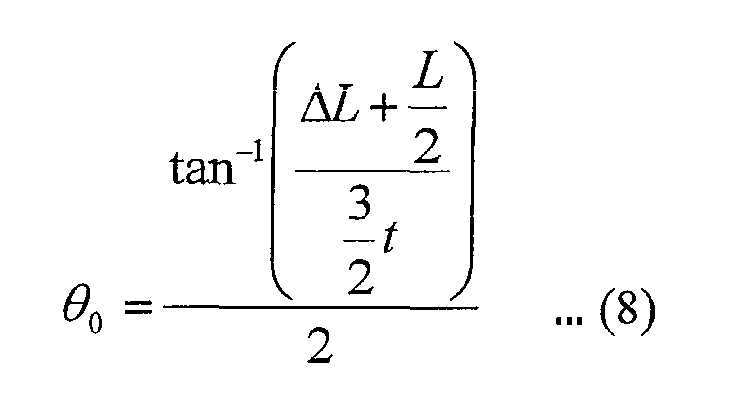
- In the region 22a near the end of the linear photoconductor 14, a tilt angle '0 of the planes of the light reflection portions 20d is set with a position of L/6 of a distance from the ends of the linear photoconductor 14 set as a standard. A tilt angle '0 of the planes of the light reflection portions 20d is set so that light incident directly on the light reflection portions 20d from the LED 12a is totally reflected on the light reflection portions 20d and exits from the exit side of the linear photoconductor 14. The following formula is given.
- By transforming Formula 9, a tilt angle '0 of the planes of the light reflection portions 20d is expressed by the following formula.

- Here, when Formula 8 and Formula 10 are compared with each other, a value of ΔL is very small, and ΔL and 3 ΔL are ignorable. The following formula is given.
- Accordingly, in the region 22a near the ends of the linear photoconductor 14 as well, a tilt angle 0 of the planes of the light reflection portions 20d may be set by using Formula 8. Thus, in the present embodiment, a tilt angle of the planes of the light reflection portions 20f containing the center of the linear photoconductor 14, and a tilt angle of the planes of the light reflection portions 20d of the region 22a near the ends of the linear photoconductor 14 may be equally set to be 0.
- In the region 22b between the region 22a and the region 22c, a tilt angle 1 of the planes of the light reflection portions 20e is set with a position (XC) of the center of the region 22b set as a standard. A tilt angle 1 of the planes of the light reflection portions 20e is set so that light incident directly on the light reflection portions 20e from the LED 12a is totally reflected on the light reflection portions 20e and exit from the exit side of the linear photoconductor 14. Then the following formula is given.
- By transforming Formula 12, a tilt angle 1 of the planes of the light reflection portions 20e is expressed by the following formula.

- Examples of set values of tilt angles of the planes of the light reflection portions of the lighting apparatus according to the present embodiment will be explained with reference to FIG. 13. FIG. 13 is a graph of the examples of tilt angles of the planes of the light reflection portions given by using the above-described formula. Distances X(n) from the end surfaces of the linear photoconductor to the light reflection portions are shown on the horizontal line. Tilt angles of the planes of the light reflection portions are shown on the vertical axis.
- The same conditions as before were again used for calculating the tilt angles (n).
- When tilt angles 0, 1 of the planes of the light deflection portions 20d-20f are set by using Formula 8 and Formula 13, the light intensity distribution shown in FIG. 13 can be obtained. FIG. 13 is a graph of an example of the light intensity distribution of the lighting apparatus according to the present embodiment. Positions with respect to the center of the linear photoconductor 14 are shown on the horizontal axis. Light intensities produced when the liquid crystal display is viewed at a distance of 350 mm are shown on the vertical axis.
- In the present embodiment, because tilt angles 0, 1 of the planes of the light reflection portions 20d, 20e, 20f are uniformly the same among the divided regions 22a, 22b, 22c, as positions of the light reflection portions 20d, 20e, 20f become further from the standard positions L/2, Xc, L/6, exit angles at which light exit from the linear photoconductor 14 gradually become larger. Thus, the present embodiment provides the light intensity distribution shown in FIG. 14.
- As seen in FIG. 14, the present embodiment cannot make the light intensity distribution as uniform as the first to the third embodiments, but in comparison with that of the proposed lighting apparatus shown in FIG. 29, the light intensity distribution of this embodiment is far more uniform.
- As described above, it is one major characteristic of the lighting apparatus according to the present embodiment that the linear photoconductor 14 is longitudinally divided in a plurality of regions 22a, 22b, 22c, and tilt angles of the planes of the light reflection portions 20d-20f are set to be the same among the sub-regions 22a, 22b, 22c.
- Setting tilt angles of the light reflection portions corresponding to positions of the light reflection portions as in the first to the third embodiments will increase costs of preparing a mould or the like for forming the linear photoconductor.
- In contrast to this, according to the present embodiment, tilt angles of the planes of the light reflection portions 20d, 20e, 20f are set at two kinds 0 and 1, and are very few. This makes it possible to reduce costs of preparing a mould, etc. for casting the linear photoconductor. As described above, the lighting apparatus according to the present embodiment can provide a uniform light intensity distribution simply and at low cost.
- The lighting apparatus according to a fifth embodiment of the present invention will be explained with reference to FIGs. 15 to 17. FIG. 15 is a plan view of the lighting apparatus according to the present embodiment. FIG. 16 is a graph of examples of tilt angles of the planes of light reflection portions of the lighting apparatus according to the present embodiment. FIG. 17 is a graph of the light intensity distribution of the lighting apparatus according to the present embodiment.
- The lighting apparatus according to the present embodiment is characterized mainly in that a linear photoconductor 14 is longitudinally further divided than that of the fourth embodiment. Tilt angles of the planes of a plurality of light reflection portions 20d, 20f, 20g, 20h formed respectively in the regions 22a, 22c, 22d, 22e are set to be the same among the divided regions 22a, 22c, 22d, 22e.
- The light reflection portions 20d, 20f, 20g, 20h are formed respectively in large numbers on the reflection side of the linear photoconductor 14, but only a few are shown in FIG. 15.
- In the region 22d, a tilt angle 1 of the planes of light reflection portions 20g is set with a position XC1 which is the center of the region 22d set as a standard.
- A tilt angle 1 of the planes of the light reflection portions 20g is set so that light incident directly on the light reflections 20g from an LED 12a is totally reflected from the planes of the light reflection portions 20g and exits from the exit side of the linear photoconductor 14. Then the following formula is given.
- By transforming Formula 14, a tilt angle 1 of the planes of the light reflection portions 20g is expressed by the following formula.

- In the region 22h, a tilt angle 2 of the planes of the light reflection portions 20h is set with a position Xc2 of the center of the region 22h set as a standard. A tilt angle 2 of the plane of the light reflection region 20h is set so that light totally reflected on the exit side of the linear photoconductor 14 is further totally reflected and exits from the exit side of the linear photoconductor 14. Then, the following formula is given.
- By transforming Formula 16, a tilt angle 2 of the planes of the light reflection portions 20h is expressed by the following formula.

- Next, examples of set values of tilt angles of the planes of the light reflection portions of the lighting apparatus according to the present embodiment will be explained with reference to FIG. 16. FIG. 16 is a graph of the examples of tilt angles of the light reflection portions given by using the above-described formula. Distances X(n) from the end surfaces of the linear photoconductor and the light reflection portions are shown on the horizontal axis. Title angles of the planes of the light reflection portions are shown on the vertical axis.
- Once again, the tilt angles (n) were calculated under the same conditions as in the first embodiment.
- In the present embodiment, tilt angles 0, 1, 2 of the planes of the light reflection portions 20d, 20f, 20g, 20h are uniformly set to be the same among the divided regions 22a, 22c, 22d, 22e. Accordingly, as positions of the light reflection portions 20d, 20f, 20g, 20h become further from the standard positions L/2, XC1, XC2, L/6, exit angles at which light rays exit from the linear photoconductor 14 gradually become larger. Thus, the present embodiment has the light intensity distribution shown in FIG. 17.
- As seen in FIG. 17, in comparison with the light intensity distribution of the lighting apparatus according to the fourth embodiment shown in FIG. 14, the light intensity distribution of the present embodiment has a smaller difference between a high light intensity and a low light intensity.
- Based on this, according to the present embodiment, in comparison with the fourth embodiment, a difference between a high light intensity and a low light intensity can be small.
- As described above, according to the present embodiment, because the photoconductor is longitudinally divided into smaller regions than in the fourth embodiment, a difference between a high light intensity and a low light intensity can be smaller in comparison with that of the fourth embodiment.
- The lighting apparatus according to a modification of the present invention will be explained with reference to FIG. 18. FIG. 18 is a plan view of the lighting apparatus according to the present modification.
- The lighting apparatus according to the present modification is mainly characterized in that in a bordering region between a region 22d and a region 22e, a light reflection portion 20g having a tilt angle 1 and a light reflection region 20h having a tilt angle 2 are alternately formed, whereby an extreme light intensity difference at the border between the region 22d and the region 22e can be prevented.
- The lighting apparatus according to a sixth embodiment of the present invention will be explained with reference to FIG. 19. FIG. 19 is a plan view of the lighting apparatus according to the present embodiment.
- In this embodiment, a reflection means 24 which is separate from the linear photoconductor 14 is disposed on the reflection side of the linear photoconductor 14, i.e., the side where light reflection portions 20 are formed, as shown in FIG. 19. The reflection means 24 can be a holder or similar of aluminum covering at least the reflection side of the linear photoconductor 14.
- In the first to the fifth embodiments, the reflection coating 20 is formed on the reflection side of the linear photoconductor 14 to prevent light from leaking out of the linear photoconductor 14. However, in the present embodiment, the reflection means 24 disposed separate from the linear photoconductor 14 returns into the linear photoconductor 14 light leaking from the reflection side of the linear photoconductor 14.
- Thus, the reflection means 24 provided in place of the reflection coating 20 can return into the linear photoconductor 14 light leaking from the reflection side of the linear photoconductor 14, whereby reduction in brightness due to light leakage is avoided.
- As described above, it is not essential to form the reflection coating on the reflection side of the linear photoconductor 14. As in the present embodiment, the reflection means 24 may be provided separate from the linear photoconductor 14.
- The lighting apparatus according to a seventh embodiment of the present invention will be explained with reference to FIG. 20. FIG. 20 is a perspective view of the lighting apparatus according to the present embodiment.
- The lighting apparatus according to the present embodiment is characterized mainly in that light reflection portions 20j are obliquely extended longitudinally in a linear photoconductor 14.
- In the lighting apparatus according to the first to the sixth embodiments, the light reflection portions 20 are perpendicularly extended longitudinally in the linear photoconductor 14. In the present embodiment, however, the light reflection portions 20j are obliquely extended longitudinally in the linear photoconductor 14. In this way the light intensity distribution can be made further uniform.
- The lighting apparatus according to an eighth embodiment of the present invention will be explained with reference to FIG. 21. FIG. 21 is a plan view of the lighting apparatus according to this embodiment, in which the reflection side of a linear photoconductor 14a, i.e., the side where light reflection portions 20 are formed, is curved.
- In the lighting apparatus according to the first to the seventh embodiments, light from the LEDs 12a, 12b can be often hindered from entering those of the light reflection portions 20 remote from the LEDs 12a, 12b, by the other light reflection portions 20.
- In contrast to this, according to the present embodiment, because the reflection side of the linear photoconductor 14a is curved, light can be incident even on those of the light reflection portions 20 remote from the LEDs 12a, 12b without being hindered by the other light reflection portions 20. Thus, the lighting apparatus according to the present embodiment can provide an even more uniform light intensity distribution.
- The lighting apparatus according to a ninth embodiment of the present invention will be explained with reference to FIG. 22. FIG. 22 is a plan view of the lighting apparatus according to the present embodiment.
- The lighting apparatus according to the present embodiment is characterized mainly in that the areas of light reflection portions 20 are increased for the portions 20 remoter from LED 12a, 12b, i.e., grooves forming the light reflection portions 20 are deeper as the grooves are remoter from the LEDs 12a, 12b.
- As shown in FIG. 22, grooves forming light reflection portions 20, which are near LEDs 12a, 12b have a depth set to be d1, and as grooves forming the light reflection portions 20 lie further from the LEDs 12a, 12b, their depths are larger. At the center of the linear photoconductor 14a, the groove forming the light reflection portions 20 has a depth d2 which is larger than the depth d1.
- In the lighting apparatus according to the first to the seventh embodiments, light from the LEDs 12a, 12b can be often hindered from entering those of the light reflection portions 20 remote from the LEDs 12a, 12b, by the other light reflection portions 20.
- In contrast to this, in the present embodiment, the width of the planes of the light reflection portions 20 is increased with distance from the LEDs 12a, 12b, whereby light can be incident on even those of the light reflection portions 20 remote from the LEDs 12a, 12b without being hindered by the other light reflection portions 20.
- The lighting apparatus according to a tenth embodiment of the present invention will be explained with reference to FIG. 23. FIG. 23 is a perspective view of the lighting apparatus according to the present embodiment.
- The lighting apparatus according to the present embodiment is characterized mainly in that a region of a linear photoconductor 14 on the reflection side thereof is divided into upper and a lower stages, i.e., the linear photoconductor 14 on the reflection side thereof is divided perpendicularly to its longitudinal direction, and tilt angles of light reflection portions 20k in the upper region 22f are uniformly set to be 0, and tilt angles of light reflection portions 221 in the lower region 22g are uniformly set to be 1.
- In the lighting apparatus according to the fourth and the fifth embodiments, the linear photoconductor 14 is longitudinally divided into sub-regions, but in the present embodiment, the linear photoconductor 14 is divided in a plurality of upper and lower regions, i.e., the linear photoconductor 14 is divided transversely to its longitudinal direction.
- Even in the case that the linear photoconductor is thus divided vertically in a plurality of regions, a light intensity distribution can be made uniform even when tilt angles of the light reflection portions of the divided regions are set to be uniformly the same.
- The lighting apparatus according to an eleventh embodiment of the present invention will be explained with reference to FIGs. 24 and 25. FIG. 24 is a perspective view of the lighting apparatus according to the present embodiment. FIG. 25 is a graph of examples of tilt angles of the planes of the right reflection portions of the lighting apparatus according to the present embodiment.
- The lighting apparatus according to the present embodiment is characterized mainly in that V-shaped grooves forming light reflection portions 20m, 20n have the same configuration, and the light reflection portions 20m disposed on the left side of the center of a linear photoconductor 14 as viewed in the drawing have the planes on the left side as viewed in the drawing set at a tilt angle L(n) so that light emitted by an LED 12a disposed on the left side as viewed in the drawing exit vertically to the longitudinal direction of the linear photoconductor 14, and the light reflection portions 20n disposed on the right side of the center of the linear photoconductor 14 as viewed in the drawing have the planes on the right side as viewed in the drawing set at a tilt angle R(n) so that light emitted by an LED 12b disposed on the right side as viewed in the drawing exit vertically to the longitudinal direction of the linear photoconductor 14.
- Large numbers of portions 20m and 20n are formed on the reflection side of the linear photoconductor 14, but only a few are shown in FIG. 24.
- As shown in FIG. 24, the light reflection portions 20m formed on the left side of the center of the linear photoconductor 14 (as viewed in the drawing) have their left-side planes set at a tilt angle L(n), so that light emitted by the left-hand LED 12a is reflected at the left-side planes of the light reflection portions 20m, and exits perpendicularly to the longitudinal direction of the linear photoconductor 14.
- A tilt angle L(n) of the planes of the light reflection portions 20m on the left side as viewed in the drawing may be set by, e.g., the above-described Formula 2 or Formula 4. In this case, the end surface of the linear photoconductor 14 on the left side as viewed in the drawing is the standard for a distance X(n).
- On the other hand, as shown in FIG. 24, the light reflection portions 20n formed on the right side of the center of the linear photoconductor 14 have their right-side planes set at a tilt angle R(n) so that light emitted by the right-hand LED 12b is reflected on the right-side planes of the light reflection portions 20n and exits perpendicularly to the longitudinal direction of the linear photoconductor 14.
- A tilt angle R(n) of the planes of the light reflection portions 20n on the right side as viewed in the drawing may be set by, e.g., the above-described Formula 2 or Formula 4. In this case, the end surface of the linear photoconductor 14 on the right side as viewed in the drawing is the standard for a distance X(n).
- Angles P formed by the planes of the V-shaped grooves forming the light reflection portions 20m, 20n are the same.
- In the present embodiment, included (subtended) angles P formed by the planes of the V-shaped grooves forming the light reflection portions are the same. A tilt angle of the planes on the right side, as viewed in the drawing, of the light reflection portions 20m is an angle given by subtracting a tilt angle L(n) and an included angle P from 180 degrees. Accordingly, light incident on the planes on the right side of the light reflection portions 20m as viewed in the drawing from the LED 12b does not always exit vertically to the longitudinal direction of the linear photoconductor 14.
- However, without any special problem, light emitted by the LED 12b is reflected on the planes on the right side, as viewed in the drawing, of the light reflection portions 20n and exits vertically to the longitudinal direction of the linear photoconductor 14.
- In the present embodiment, because included angles P of the planes of the V-shaped grooves forming the light reflection portions are set to be the same, a tilt angle of the planes on the left side, as viewed in the drawing, of the light reflection portions 20n is an angle given by subtracting a tilt angle R(n) and an included angle P from 180 degrees. Thus, light incident on the planes on the left side, as viewed in the drawing, of the light reflection portions 20n does not always exit perpendicularly to the longitudinal direction of the linear photoconductor 14.
- However, without any special problem, light incident from the LED 12a is reflected on the planes on the left side, as viewed in the drawing, of the light reflection portions 20m and exits perpendicular to the longitudinal direction of the linear photoconductor 14.
- Next, examples of set values of the tilt angles of the planes of the light reflection portions of the lighting apparatus according to the present embodiment will be explained with reference to FIG. 25. FIG. 25 is a graph of the examples of tilt angles of the light reflection portions, given by the above-described formula. Distances X(n) from the end surfaces of the linear photoconductor and the light reflection portions are shown on the horizontal axis. Tilt angles of the planes of the light reflection portions are shown on the vertical axis.
- The tilt angles were calculated under the conditions that the display size was 2 inches, display screen width was 35 mm, number of the light reflection portions 20 was 170, pitch of the light reflection portions 20 was 0.21 mm, thickness t of the linear photoconductor 14 was 3 mm, length L of the linear photoconductor 14 was 37 mm, distance ΔL between the LEDs 12a, 12b and the linear photoconductor 14 was 0 mm, refractive index of the linear photoconductor 14 was 1.51, and distance viewer to screen was 350 mm.
- According to the present embodiment, the V-shaped grooves forming the light reflection portions 20m, 20n have the same configuration. Accordingly, one kind of cutting tool for forming a mould, etc. to manufacture linear photoconductor 14 can be used. Thus, according to the present embodiment, the mould, etc. can be formed at low cost, which makes it possible to provide at low cost the lighting apparatus which can provide a uniform light intensity distribution.
- The liquid crystal display according to a twelfth embodiment of the present invention will be explained with reference to FIG. 26. FIG. 26 is a perspective view of the liquid crystal display according to the present embodiment.
- The liquid crystal display according to the present embodiment comprises a combination of the lighting apparatus according to any one of the first to the eleventh embodiments, and a reflection-type liquid crystal panel.
- As shown in FIG. 26, the lighting apparatus 10 according to any one of the first to the eleventh embodiments is provided on a reflection-type liquid crystal panel 26.
- Light exiting from the linear photoconductor 14 of the lighting apparatus 10 is incident on the reflection-type liquid crystal panel 26 via the surface photoconductor 16, is reflected on a mirror (not shown) disposed in the reflection-type liquid crystal panel 26, and enters the viewer's eye. In the present embodiment, the lighting apparatus 10 functions as a front light.
- According to the present embodiment, the liquid crystal display uses the lighting apparatus according to any one of the first to the eleventh embodiments, whereby the reflection-type liquid crystal panel can be illuminated with a uniform light intensity. Accordingly, the liquid crystal display according to the present embodiment can have good display characteristics.
- The liquid crystal display according to a thirteenth embodiment of the present invention will be explained with reference to FIG. 27. FIG. 27 is a perspective view of the liquid crystal display according to the present embodiment.
- The liquid crystal display according to the present embodiment comprises a combination of the lighting apparatus according to any one of the first to the eleventh embodiments, and a transmission-type liquid crystal panel.
- As shown in FIG. 27, a transmission-type liquid crystal panel 26 is provided on the lighting apparatus 10 (backlight) according to any one of the first to the eleventh embodiments.
- Light exiting from the linear photoconductor 14 is incident on the transmission-type liquid crystal panel 28 via the surface photoconductor 16, transmitted by the transmission-type liquid crystal panel 28, and incident on the human eye.
- As described above, according to the present embodiment, the liquid crystal display using the transmission-type liquid crystal panel can provide good display characteristics.
- The present invention is not limited to the above-described embodiments and can cover other various modifications.
- For example, in the tenth embodiment, the linear photoconductor is divided into upper and lower regions. However, the linear photoconductor may be divided into more than two regions, whereby further uniform light intensity distributions can be obtained. However, as more regions are provided, a larger number of set angles of light reflection portions are required. Accordingly, it is preferable to set a suitable number of regions in consideration of a required uniform light intensity distribution and allowable costs.
Claims (18)
- A lighting apparatus comprising a light source for emitting light, and a linear photoconductor for reflecting the light incident on a plurality of light reflection portions formed on a reflection side from the light source, and causing the light to exit linearly from an exit side opposed to the reflection side,
planes of the plurality of light reflection portions being tilted at angles which converge the light to a viewer's eye. - A lighting apparatus comprising a light source for emitting light, and a linear photoconductor for reflecting the light incident on a plurality of light reflection portions formed on a reflection side from the light source, and causing the light to exit linearly from an exit side opposed to the reflection side,
planes of the plural light reflection portions being respectively tilted so that the light exits substantially perpendicular to the longitudinal direction of the linear photoconductor. - A lighting apparatus according to claim 1 or 2, wherein
the plural light reflection portions are similar V-shaped grooves, one side of which form the planes of the light reflection portions. - A lighting apparatus according to claim 1, 2, or 3, wherein
the linear photoconductor is longitudinally divided into a plurality of regions; and
in each divided region, the planes of the plural light reflection portions are tilted at the same angle. - A lighting apparatus according to claim 4, wherein
the planes of the plural light reflection portions are tilted at the same angles in a region containing the center of the linear photoconductor and in the regions near the ends of the linear photoconductor. - A lighting apparatus according to claim 4, wherein
in a first longitudinally divided region of the linear photoconductor, the planes of the light reflection portions are tilted equally at a first angle;
in a second region adjacent to the first region, the planes of the light reflection portions are tilted equally at a second angle which is different from the first angle; and
in a region near the border between the first region and the second region, the light reflection portions having the planes tilted at the first angle and the light reflection portions having the planes tilted at the second angle are mixed. - A lighting apparatus according to claim 1, 2, or 3, wherein
the linear photoconductor is divided into a plurality of regions perpendicularly to the longitudinal direction; and
in each divided region, the planes of the plural light reflection portions are tilted at the same angle. - A lighting apparatus according to claim 1, 2, or 3, wherein
the light reflection portions extend obliquely to the longitudinal direction of the linear photoconductor. - A lighting apparatus according to claim 1, wherein
the planes of the plural light reflection portions are respectively tilted at angles which converge the light emitted substantially from the center of the light source to the viewer's eye. - A lighting apparatus according to claim 2, wherein
the planes of the plural light reflection portions are respectively tilted at angles which cause the light emitted substantially from the center of the light source to exit substantially perpendicular to the longitudinal direction of the linear photoconductor. - A lighting apparatus according to any preceding claim, further comprising
a surface photoconductor optically coupled to the linear photoconductor, for causing the light entering from the linear photoconductor to exit in plane. - A lighting apparatus according to any preceding claim, wherein
the linear photoconductor has the reflection side curved. - A lighting apparatus according to any preceding claim, wherein
the width of one plane of the light reflection portions, and the width of the other plane of the light reflection portions are different from each other. - A lighting apparatus according to any preceding claim, wherein
a reflection coating is further formed on the reflection side of the linear photoconductor. - A lighting apparatus according to any of claims 1 to 13, further comprising
reflection means provided on the reflection side of the linear photoconductor separately from the linear photoconductor. - A lighting apparatus according to any preceding claim, wherein
the linear photoconductor is formed substantially in the form of a square-section rod. - A liquid crystal display comprising a lighting apparatus including a light source for emitting light, a linear photoconductor for reflecting light incident on a plurality of light reflection portions formed on the reflection side from the light source and causing the light to exit linearly from the exit side opposed to the reflection side, and a surface photoconductor optically coupled to the linear photoconductor and causing the light entering from the linear photoconductor to exit in plane; and a liquid crystal panel illuminated by the lighting apparatus,
planes of the plural light reflection portions being tilted at an angle which converges the light to a viewer's eye. - A liquid crystal display comprising a lighting apparatus including a light source for emitting light, a linear photoconductor for reflecting light incident on a plurality of light reflection portions formed on the reflection side from the light source and causing the light to exit linearly from the exit side opposed to the reflection side, and a surface photoconductor optically coupled to the linear photoconductor and causing the light entering from the linear photoconductor to exit in plane; and a liquid crystal panel illuminated by the lighting apparatus,
planes of the plural light reflection portions being respectively tilted at angles which cause the light to exit substantially perpendicular to the longitudinal direction of the linear photoconductor.
Priority Applications (1)
| Application Number | Priority Date | Filing Date | Title |
|---|---|---|---|
| EP03016505A EP1367430B1 (en) | 2001-08-31 | 2002-03-14 | Lighting apparatus and liquid crystal display |
Applications Claiming Priority (2)
| Application Number | Priority Date | Filing Date | Title |
|---|---|---|---|
| JP2001263922 | 2001-08-31 | ||
| JP2001263922A JP4671562B2 (en) | 2001-08-31 | 2001-08-31 | Illumination device and liquid crystal display device |
Related Child Applications (2)
| Application Number | Title | Priority Date | Filing Date |
|---|---|---|---|
| EP03016505A Division EP1367430B1 (en) | 2001-08-31 | 2002-03-14 | Lighting apparatus and liquid crystal display |
| EP03016505A Division-Into EP1367430B1 (en) | 2001-08-31 | 2002-03-14 | Lighting apparatus and liquid crystal display |
Publications (2)
| Publication Number | Publication Date |
|---|---|
| EP1288702A1 true EP1288702A1 (en) | 2003-03-05 |
| EP1288702B1 EP1288702B1 (en) | 2004-12-29 |
Family
ID=19090601
Family Applications (2)
| Application Number | Title | Priority Date | Filing Date |
|---|---|---|---|
| EP02251845A Expired - Fee Related EP1288702B1 (en) | 2001-08-31 | 2002-03-14 | Lighting apparatus and liquid crystal display |
| EP03016505A Expired - Fee Related EP1367430B1 (en) | 2001-08-31 | 2002-03-14 | Lighting apparatus and liquid crystal display |
Family Applications After (1)
| Application Number | Title | Priority Date | Filing Date |
|---|---|---|---|
| EP03016505A Expired - Fee Related EP1367430B1 (en) | 2001-08-31 | 2002-03-14 | Lighting apparatus and liquid crystal display |
Country Status (8)
| Country | Link |
|---|---|
| US (1) | US6883924B2 (en) |
| EP (2) | EP1288702B1 (en) |
| JP (1) | JP4671562B2 (en) |
| KR (1) | KR100817097B1 (en) |
| CN (3) | CN1920640A (en) |
| CA (2) | CA2376387C (en) |
| DE (2) | DE60208934T2 (en) |
| TW (1) | TW583436B (en) |
Cited By (4)
| Publication number | Priority date | Publication date | Assignee | Title |
|---|---|---|---|---|
| EP1531302A1 (en) * | 2002-08-23 | 2005-05-18 | Fujitsu Limited | Illuminator and liquid crystal display |
| WO2005054936A1 (en) * | 2003-12-05 | 2005-06-16 | Nokia Corporation | A display and a method of providing a display |
| KR100903159B1 (en) * | 2006-07-04 | 2009-06-17 | 노키아 코포레이션 | A display and a method of providing a display |
| CN111256094A (en) * | 2020-01-22 | 2020-06-09 | 广州市焦汇光电科技有限公司 | Optical device, optical system and optical curtain wall projection system |
Families Citing this family (56)
| Publication number | Priority date | Publication date | Assignee | Title |
|---|---|---|---|---|
| JP4185721B2 (en) * | 2002-07-17 | 2008-11-26 | アルプス電気株式会社 | Illumination device and liquid crystal display device |
| EP1566590B1 (en) * | 2002-11-29 | 2011-07-13 | Fujitsu Limited | Illumination device and liquid crystal display device |
| JP2004200128A (en) * | 2002-12-20 | 2004-07-15 | Koninkl Philips Electronics Nv | Auxiliary light source and front light using it |
| TWI289708B (en) | 2002-12-25 | 2007-11-11 | Qualcomm Mems Technologies Inc | Optical interference type color display |
| TWM243658U (en) * | 2003-06-13 | 2004-09-11 | Hon Hai Prec Ind Co Ltd | Planar light source device |
| US6929391B2 (en) * | 2003-07-17 | 2005-08-16 | Apple Computer, Inc. | Light guide panel and method of use |
| AU2003257833A1 (en) * | 2003-08-13 | 2005-03-07 | Fujitsu Limited | Illuminating device and liquid crystal display unit |
| CN100371789C (en) * | 2004-01-14 | 2008-02-27 | 统宝光电股份有限公司 | Area light source structure |
| US7342705B2 (en) | 2004-02-03 | 2008-03-11 | Idc, Llc | Spatial light modulator with integrated optical compensation structure |
| JP2005308789A (en) * | 2004-04-16 | 2005-11-04 | Alps Electric Co Ltd | Reflector and liquid crystal display device using the same |
| US7561323B2 (en) * | 2004-09-27 | 2009-07-14 | Idc, Llc | Optical films for directing light towards active areas of displays |
| US7813026B2 (en) * | 2004-09-27 | 2010-10-12 | Qualcomm Mems Technologies, Inc. | System and method of reducing color shift in a display |
| US7355780B2 (en) | 2004-09-27 | 2008-04-08 | Idc, Llc | System and method of illuminating interferometric modulators using backlighting |
| US7750886B2 (en) * | 2004-09-27 | 2010-07-06 | Qualcomm Mems Technologies, Inc. | Methods and devices for lighting displays |
| JP4553726B2 (en) * | 2004-12-28 | 2010-09-29 | 富士通株式会社 | Rod-shaped light guide, illumination device, and liquid crystal display device |
| JP2007041605A (en) * | 2005-08-04 | 2007-02-15 | Boe Hydis Technology Co Ltd | Backlight structure for liquid crystal display device |
| US7603001B2 (en) * | 2006-02-17 | 2009-10-13 | Qualcomm Mems Technologies, Inc. | Method and apparatus for providing back-lighting in an interferometric modulator display device |
| EP1980882A3 (en) * | 2006-10-06 | 2012-12-12 | QUALCOMM MEMS Technologies, Inc. | Thin light bar and method of manufacturing |
| US8107155B2 (en) * | 2006-10-06 | 2012-01-31 | Qualcomm Mems Technologies, Inc. | System and method for reducing visual artifacts in displays |
| WO2008045207A2 (en) | 2006-10-06 | 2008-04-17 | Qualcomm Mems Technologies, Inc. | Light guide |
| EP2069838A2 (en) * | 2006-10-06 | 2009-06-17 | Qualcomm Mems Technologies, Inc. | Illumination device with built-in light coupler |
| EP2366942A1 (en) | 2006-10-06 | 2011-09-21 | Qualcomm Mems Technologies, Inc. | Optical loss layer integrated in an illumination apparatus of a display |
| WO2008045310A2 (en) * | 2006-10-06 | 2008-04-17 | Qualcomm Mems Technologies, Inc. | Light bar including turning microstructures and contoured back reflector |
| KR100818278B1 (en) * | 2006-10-16 | 2008-04-01 | 삼성전자주식회사 | Illuminating device for liquid crystal display |
| US7864395B2 (en) | 2006-10-27 | 2011-01-04 | Qualcomm Mems Technologies, Inc. | Light guide including optical scattering elements and a method of manufacture |
| KR101318253B1 (en) * | 2007-03-30 | 2013-10-18 | 삼성디스플레이 주식회사 | Light guide plate and display apparatus having the same |
| US7733439B2 (en) * | 2007-04-30 | 2010-06-08 | Qualcomm Mems Technologies, Inc. | Dual film light guide for illuminating displays |
| US7949213B2 (en) | 2007-12-07 | 2011-05-24 | Qualcomm Mems Technologies, Inc. | Light illumination of displays with front light guide and coupling elements |
| US8068710B2 (en) | 2007-12-07 | 2011-11-29 | Qualcomm Mems Technologies, Inc. | Decoupled holographic film and diffuser |
| US8721149B2 (en) | 2008-01-30 | 2014-05-13 | Qualcomm Mems Technologies, Inc. | Illumination device having a tapered light guide |
| JP2011512006A (en) | 2008-01-30 | 2011-04-14 | デジタル オプティクス インターナショナル,リミティド ライアビリティ カンパニー | Thin lighting system |
| WO2009102731A2 (en) | 2008-02-12 | 2009-08-20 | Qualcomm Mems Technologies, Inc. | Devices and methods for enhancing brightness of displays using angle conversion layers |
| US8654061B2 (en) * | 2008-02-12 | 2014-02-18 | Qualcomm Mems Technologies, Inc. | Integrated front light solution |
| US8049951B2 (en) | 2008-04-15 | 2011-11-01 | Qualcomm Mems Technologies, Inc. | Light with bi-directional propagation |
| CN103149623A (en) * | 2008-05-28 | 2013-06-12 | 高通Mems科技公司 | Front light devices and methods of fabrication thereof |
| US20100051089A1 (en) * | 2008-09-02 | 2010-03-04 | Qualcomm Mems Technologies, Inc. | Light collection device with prismatic light turning features |
| US8358266B2 (en) | 2008-09-02 | 2013-01-22 | Qualcomm Mems Technologies, Inc. | Light turning device with prismatic light turning features |
| KR20110081270A (en) * | 2008-10-10 | 2011-07-13 | 퀄컴 엠이엠스 테크놀로지스, 인크. | Distributed lighting control system |
| CN102177398B (en) * | 2008-10-10 | 2015-01-28 | 高通Mems科技公司 | Distributed illumination system |
| WO2010082952A1 (en) | 2009-01-13 | 2010-07-22 | Qualcomm Mems Technologies, Inc. | Large area light panel and screen |
| US20100195310A1 (en) * | 2009-02-04 | 2010-08-05 | Qualcomm Mems Technologies, Inc. | Shaped frontlight reflector for use with display |
| US8172417B2 (en) * | 2009-03-06 | 2012-05-08 | Qualcomm Mems Technologies, Inc. | Shaped frontlight reflector for use with display |
| KR20120027415A (en) * | 2009-05-29 | 2012-03-21 | 퀄컴 엠이엠스 테크놀로지스, 인크. | Illumination devices for reflective displays |
| US20100302218A1 (en) | 2009-05-29 | 2010-12-02 | Qualcomm Mems Technologies, Inc. | Illumination devices and methods of fabrication thereof |
| US20110032214A1 (en) * | 2009-06-01 | 2011-02-10 | Qualcomm Mems Technologies, Inc. | Front light based optical touch screen |
| US20110169428A1 (en) * | 2010-01-08 | 2011-07-14 | Qualcomm Mems Technologies, Inc. | Edge bar designs to mitigate edge shadow artifact |
| US8402647B2 (en) | 2010-08-25 | 2013-03-26 | Qualcomm Mems Technologies Inc. | Methods of manufacturing illumination systems |
| US8902484B2 (en) | 2010-12-15 | 2014-12-02 | Qualcomm Mems Technologies, Inc. | Holographic brightness enhancement film |
| CN202165943U (en) * | 2011-07-21 | 2012-03-14 | 北京京东方光电科技有限公司 | Backlight and display device |
| KR101968552B1 (en) * | 2011-11-18 | 2019-04-15 | 삼성디스플레이 주식회사 | Touch display apparatus and method of determining touch position using the same |
| TWI477855B (en) * | 2012-01-20 | 2015-03-21 | Au Optronics Corp | Backlight module |
| WO2014076914A1 (en) * | 2012-11-14 | 2014-05-22 | パナソニック株式会社 | Light source device |
| US9423552B2 (en) | 2014-02-24 | 2016-08-23 | Google Inc. | Lightguide device with outcoupling structures |
| JP6689000B2 (en) | 2014-11-10 | 2020-04-28 | パナソニックIpマネジメント株式会社 | Lighting device for vacuum cleaner |
| KR102019888B1 (en) * | 2019-04-05 | 2019-11-05 | 삼성디스플레이 주식회사 | Touch display apparatus and method of determining touch position using the same |
| JP7225272B2 (en) * | 2021-01-12 | 2023-02-20 | 矢崎総業株式会社 | vehicle display |
Citations (5)
| Publication number | Priority date | Publication date | Assignee | Title |
|---|---|---|---|---|
| US5664862A (en) * | 1994-11-29 | 1997-09-09 | Precision Lamp, Inc. | Edge light for panel display |
| EP0866264A1 (en) * | 1997-03-18 | 1998-09-23 | Seiko Epson Corporation | Lighting device, liquid crystal display unit, and electronic equipment |
| US5894539A (en) * | 1994-06-24 | 1999-04-13 | Minnesota Mining And Manufacturing Company | Line light source having light pipe with rectangular cross-section |
| EP0969311A1 (en) * | 1998-06-29 | 2000-01-05 | Minebea Co., Ltd. | Spread illuminating apparatus |
| JP2001035227A (en) * | 1999-07-19 | 2001-02-09 | Minebea Co Ltd | Flat lighting system |
Family Cites Families (16)
| Publication number | Priority date | Publication date | Assignee | Title |
|---|---|---|---|---|
| JPH07294745A (en) * | 1994-04-25 | 1995-11-10 | Fanuc Ltd | Back light panel |
| US5980054A (en) * | 1996-05-09 | 1999-11-09 | Matsushita Electric Industrial Co., Ltd. | Panel-form illuminating system |
| JPH11271767A (en) * | 1998-03-20 | 1999-10-08 | Stanley Electric Co Ltd | Liquid crystal display device with lighting |
| JP2000089031A (en) * | 1998-09-10 | 2000-03-31 | Sanyo Electric Co Ltd | Back light device and surface light emitting device |
| CN2358336Y (en) | 1998-10-08 | 2000-01-12 | 广州市荔湾区华安堡电子灯饰厂 | Luminous reflecting plate with light-emitting diode |
| CN1877191B (en) * | 1998-11-27 | 2011-08-17 | 夏普株式会社 | Illuminator |
| JP3421603B2 (en) * | 1999-01-21 | 2003-06-30 | 三洋電機株式会社 | Light guide plate, surface light source device and display device using the light guide plate |
| JP3366589B2 (en) * | 1999-01-28 | 2003-01-14 | 京セラ株式会社 | Liquid crystal display |
| TW592308U (en) * | 1999-02-17 | 2004-06-11 | Enplas Corp | Light guiding plate, surface light source device, and liquid crystal display device |
| JP2000268616A (en) * | 1999-03-15 | 2000-09-29 | Seiko Epson Corp | Flat emitter, front light, liquid crystal device and electronic apparatus |
| JP2000268622A (en) * | 1999-03-16 | 2000-09-29 | Minebea Co Ltd | Planar lighting system |
| JP2001014921A (en) * | 1999-06-28 | 2001-01-19 | Minebea Co Ltd | Surface lighting system |
| JP2001043718A (en) * | 1999-07-28 | 2001-02-16 | Citizen Electronics Co Ltd | Surface light source unit and liquid crystal display device using the same |
| JP2001236811A (en) * | 2000-02-23 | 2001-08-31 | Fujitsu Kasei Kk | Illumination device |
| JP4404424B2 (en) * | 2000-01-21 | 2010-01-27 | シチズン電子株式会社 | Linear light source unit |
| JP2001222906A (en) | 2000-02-08 | 2001-08-17 | Minebea Co Ltd | Flat lighting system |
-
2001
- 2001-08-31 JP JP2001263922A patent/JP4671562B2/en not_active Expired - Fee Related
-
2002
- 2002-03-06 US US10/092,167 patent/US6883924B2/en not_active Expired - Lifetime
- 2002-03-07 TW TW091104284A patent/TW583436B/en not_active IP Right Cessation
- 2002-03-11 CA CA2376387A patent/CA2376387C/en not_active Expired - Fee Related
- 2002-03-11 CA CA2692580A patent/CA2692580C/en not_active Expired - Fee Related
- 2002-03-14 DE DE60208934T patent/DE60208934T2/en not_active Expired - Lifetime
- 2002-03-14 DE DE60202410T patent/DE60202410T2/en not_active Expired - Lifetime
- 2002-03-14 EP EP02251845A patent/EP1288702B1/en not_active Expired - Fee Related
- 2002-03-14 EP EP03016505A patent/EP1367430B1/en not_active Expired - Fee Related
- 2002-03-15 KR KR1020020014122A patent/KR100817097B1/en not_active IP Right Cessation
- 2002-04-09 CN CNA2006100817874A patent/CN1920640A/en active Pending
- 2002-04-09 CN CN02106197A patent/CN1403858A/en active Pending
- 2002-04-09 CN CNA2007101537184A patent/CN101118044A/en active Pending
Patent Citations (6)
| Publication number | Priority date | Publication date | Assignee | Title |
|---|---|---|---|---|
| US5894539A (en) * | 1994-06-24 | 1999-04-13 | Minnesota Mining And Manufacturing Company | Line light source having light pipe with rectangular cross-section |
| US5664862A (en) * | 1994-11-29 | 1997-09-09 | Precision Lamp, Inc. | Edge light for panel display |
| EP0866264A1 (en) * | 1997-03-18 | 1998-09-23 | Seiko Epson Corporation | Lighting device, liquid crystal display unit, and electronic equipment |
| EP0969311A1 (en) * | 1998-06-29 | 2000-01-05 | Minebea Co., Ltd. | Spread illuminating apparatus |
| JP2001035227A (en) * | 1999-07-19 | 2001-02-09 | Minebea Co Ltd | Flat lighting system |
| US6293683B1 (en) * | 1999-07-19 | 2001-09-25 | Minebea Co. Ltd. | Spread illuminating apparatus |
Non-Patent Citations (1)
| Title |
|---|
| PATENT ABSTRACTS OF JAPAN vol. 2000, no. 19 5 June 2001 (2001-06-05) * |
Cited By (7)
| Publication number | Priority date | Publication date | Assignee | Title |
|---|---|---|---|---|
| EP1531302A1 (en) * | 2002-08-23 | 2005-05-18 | Fujitsu Limited | Illuminator and liquid crystal display |
| EP1531302A4 (en) * | 2002-08-23 | 2005-08-31 | Fujitsu Ltd | Illuminator and liquid crystal display |
| US7108417B2 (en) | 2002-08-23 | 2006-09-19 | Fujitsu Limited | Lighting apparatus and liquid crystal display |
| WO2005054936A1 (en) * | 2003-12-05 | 2005-06-16 | Nokia Corporation | A display and a method of providing a display |
| KR100903159B1 (en) * | 2006-07-04 | 2009-06-17 | 노키아 코포레이션 | A display and a method of providing a display |
| CN111256094A (en) * | 2020-01-22 | 2020-06-09 | 广州市焦汇光电科技有限公司 | Optical device, optical system and optical curtain wall projection system |
| CN111256094B (en) * | 2020-01-22 | 2022-09-23 | 广州市焦汇光电科技有限公司 | Optical device, optical system and optical curtain wall projection system |
Also Published As
| Publication number | Publication date |
|---|---|
| DE60208934T2 (en) | 2006-07-27 |
| DE60208934D1 (en) | 2006-04-13 |
| EP1367430B1 (en) | 2006-01-25 |
| EP1288702B1 (en) | 2004-12-29 |
| US20030058632A1 (en) | 2003-03-27 |
| EP1367430A2 (en) | 2003-12-03 |
| TW583436B (en) | 2004-04-11 |
| CA2376387C (en) | 2010-05-04 |
| US6883924B2 (en) | 2005-04-26 |
| CN101118044A (en) | 2008-02-06 |
| DE60202410D1 (en) | 2005-02-03 |
| KR100817097B1 (en) | 2008-03-26 |
| KR20030019064A (en) | 2003-03-06 |
| CN1403858A (en) | 2003-03-19 |
| CA2692580A1 (en) | 2003-02-28 |
| DE60202410T2 (en) | 2005-06-30 |
| CN1920640A (en) | 2007-02-28 |
| JP4671562B2 (en) | 2011-04-20 |
| JP2003077326A (en) | 2003-03-14 |
| CA2692580C (en) | 2015-09-15 |
| EP1367430A3 (en) | 2004-05-26 |
| CA2376387A1 (en) | 2003-02-28 |
Similar Documents
| Publication | Publication Date | Title |
|---|---|---|
| EP1288702A1 (en) | Lighting apparatus and liquid crystal display | |
| EP1531302A1 (en) | Illuminator and liquid crystal display | |
| US9268148B2 (en) | Light source device and stereoscopic display apparatus | |
| US20060164861A1 (en) | Lighting apparatus and liquid crystal display | |
| US20020003711A1 (en) | Displaying apparatus | |
| KR20050033470A (en) | Plane light source and liquid crystal display device using the plane light source | |
| US20070133094A1 (en) | Optical film, illuminator and display | |
| CN111323961A (en) | Optical structure and display device | |
| CN103912823A (en) | Backlight assembly and a display device using the same | |
| US20120051032A1 (en) | Light emission angle adjusting sheet, display panel, display device, and method for manufacturing light emission angle adjusting sheet | |
| KR100706153B1 (en) | Pole type light guide, illumination device and liquid crystal display device | |
| JP4483233B2 (en) | Surface light source and liquid crystal display device | |
| US10564458B2 (en) | Connecting member and display including connecting member | |
| KR100782680B1 (en) | Illuminating device and liquid crystal display unit | |
| JP5454454B2 (en) | Illumination device and liquid crystal display device | |
| KR102642698B1 (en) | Light source with bipartite emission pattern, multi-view backlight, and method | |
| KR20050023350A (en) | Illuminator and liquid crystal display | |
| KR20050042189A (en) | Illumination device and liquid crystal display device | |
| KR20020030065A (en) | Light guide pannel for sheetless back light unit or front light unit |
Legal Events
| Date | Code | Title | Description |
|---|---|---|---|
| PUAI | Public reference made under article 153(3) epc to a published international application that has entered the european phase |
Free format text: ORIGINAL CODE: 0009012 |
|
| AK | Designated contracting states |
Kind code of ref document: A1 Designated state(s): AT BE CH CY DE DK ES FI FR GB GR IE IT LI LU MC NL PT SE TR |
|
| AX | Request for extension of the european patent |
Extension state: AL LT LV MK RO SI |
|
| 17P | Request for examination filed |
Effective date: 20030120 |
|
| 17Q | First examination report despatched |
Effective date: 20030414 |
|
| AKX | Designation fees paid |
Designated state(s): DE FR GB |
|
| GRAP | Despatch of communication of intention to grant a patent |
Free format text: ORIGINAL CODE: EPIDOSNIGR1 |
|
| GRAS | Grant fee paid |
Free format text: ORIGINAL CODE: EPIDOSNIGR3 |
|
| GRAA | (expected) grant |
Free format text: ORIGINAL CODE: 0009210 |
|
| AK | Designated contracting states |
Kind code of ref document: B1 Designated state(s): DE FR GB |
|
| REG | Reference to a national code |
Ref country code: GB Ref legal event code: FG4D |
|
| REG | Reference to a national code |
Ref country code: IE Ref legal event code: FG4D |
|
| REF | Corresponds to: |
Ref document number: 60202410 Country of ref document: DE Date of ref document: 20050203 Kind code of ref document: P |
|
| PLBE | No opposition filed within time limit |
Free format text: ORIGINAL CODE: 0009261 |
|
| STAA | Information on the status of an ep patent application or granted ep patent |
Free format text: STATUS: NO OPPOSITION FILED WITHIN TIME LIMIT |
|
| ET | Fr: translation filed | ||
| 26N | No opposition filed |
Effective date: 20050930 |
|
| REG | Reference to a national code |
Ref country code: DE Ref legal event code: R082 Ref document number: 60202410 Country of ref document: DE Representative=s name: REICHERT & LINDNER PARTNERSCHAFT PATENTANWAELT, DE |
|
| REG | Reference to a national code |
Ref country code: DE Ref legal event code: R081 Ref document number: 60202410 Country of ref document: DE Owner name: FUJITSU LIMITED, JP Free format text: FORMER OWNER: FUJITSU LTD., FUJITSU KASEI LTD., , JP Effective date: 20150108 Ref country code: DE Ref legal event code: R082 Ref document number: 60202410 Country of ref document: DE Representative=s name: REICHERT & LINDNER PARTNERSCHAFT PATENTANWAELT, DE Effective date: 20150108 Ref country code: DE Ref legal event code: R081 Ref document number: 60202410 Country of ref document: DE Owner name: FUJITSU LIMITED, JP Free format text: FORMER OWNERS: FUJITSU LTD., KAWASAKI-SHI, KANAGAWA-KEN, JP; FUJITSU KASEI LTD., YOKOHAMA, KANAGAWA, JP Effective date: 20150108 Ref country code: DE Ref legal event code: R081 Ref document number: 60202410 Country of ref document: DE Owner name: FUJITSU LIMITED, KAWASAKI-SHI, JP Free format text: FORMER OWNERS: FUJITSU LIMITED, KAWASAKI-SHI, KANAGAWA, JP; FUJITSU KASEI LTD., YOKOHAMA, KANAGAWA, JP Effective date: 20150108 |
|
| REG | Reference to a national code |
Ref country code: FR Ref legal event code: PLFP Year of fee payment: 15 |
|
| REG | Reference to a national code |
Ref country code: GB Ref legal event code: 732E Free format text: REGISTERED BETWEEN 20160204 AND 20160210 |
|
| REG | Reference to a national code |
Ref country code: FR Ref legal event code: TP Owner name: FUJITSU KAISEI LIMITED, JP Effective date: 20160224 |
|
| REG | Reference to a national code |
Ref country code: FR Ref legal event code: PLFP Year of fee payment: 16 |
|
| PGFP | Annual fee paid to national office [announced via postgrant information from national office to epo] |
Ref country code: FR Payment date: 20170213 Year of fee payment: 16 Ref country code: DE Payment date: 20170307 Year of fee payment: 16 |
|
| PGFP | Annual fee paid to national office [announced via postgrant information from national office to epo] |
Ref country code: GB Payment date: 20170308 Year of fee payment: 16 |
|
| REG | Reference to a national code |
Ref country code: DE Ref legal event code: R119 Ref document number: 60202410 Country of ref document: DE |
|
| GBPC | Gb: european patent ceased through non-payment of renewal fee |
Effective date: 20180314 |
|
| PG25 | Lapsed in a contracting state [announced via postgrant information from national office to epo] |
Ref country code: DE Free format text: LAPSE BECAUSE OF NON-PAYMENT OF DUE FEES Effective date: 20181002 |
|
| PG25 | Lapsed in a contracting state [announced via postgrant information from national office to epo] |
Ref country code: GB Free format text: LAPSE BECAUSE OF NON-PAYMENT OF DUE FEES Effective date: 20180314 |
|
| PG25 | Lapsed in a contracting state [announced via postgrant information from national office to epo] |
Ref country code: FR Free format text: LAPSE BECAUSE OF NON-PAYMENT OF DUE FEES Effective date: 20180331 |