EP1289023A2 - Nonvolatile semiconductor memory device, fabricating method thereof and operation method thereof - Google Patents
Nonvolatile semiconductor memory device, fabricating method thereof and operation method thereof Download PDFInfo
- Publication number
- EP1289023A2 EP1289023A2 EP02019493A EP02019493A EP1289023A2 EP 1289023 A2 EP1289023 A2 EP 1289023A2 EP 02019493 A EP02019493 A EP 02019493A EP 02019493 A EP02019493 A EP 02019493A EP 1289023 A2 EP1289023 A2 EP 1289023A2
- Authority
- EP
- European Patent Office
- Prior art keywords
- control gate
- semiconductor substrate
- selected cell
- supplying
- voltage
- Prior art date
- Legal status (The legal status is an assumption and is not a legal conclusion. Google has not performed a legal analysis and makes no representation as to the accuracy of the status listed.)
- Withdrawn
Links
- 239000004065 semiconductor Substances 0.000 title claims abstract description 172
- 238000000034 method Methods 0.000 title claims description 64
- 239000000758 substrate Substances 0.000 claims abstract description 135
- 238000007667 floating Methods 0.000 claims abstract description 112
- 238000009792 diffusion process Methods 0.000 claims abstract description 70
- 239000002344 surface layer Substances 0.000 claims abstract description 6
- 239000004020 conductor Substances 0.000 claims description 26
- 239000012535 impurity Substances 0.000 claims description 17
- 238000002955 isolation Methods 0.000 claims description 8
- 230000015572 biosynthetic process Effects 0.000 claims description 4
- 125000006850 spacer group Chemical group 0.000 claims description 4
- 239000010410 layer Substances 0.000 description 20
- XUIMIQQOPSSXEZ-UHFFFAOYSA-N Silicon Chemical compound [Si] XUIMIQQOPSSXEZ-UHFFFAOYSA-N 0.000 description 17
- 238000004519 manufacturing process Methods 0.000 description 17
- 229910052710 silicon Inorganic materials 0.000 description 17
- 239000010703 silicon Substances 0.000 description 17
- 229910021420 polycrystalline silicon Inorganic materials 0.000 description 15
- 229910052581 Si3N4 Inorganic materials 0.000 description 14
- 229920005591 polysilicon Polymers 0.000 description 14
- 229910052814 silicon oxide Inorganic materials 0.000 description 14
- VYPSYNLAJGMNEJ-UHFFFAOYSA-N Silicium dioxide Chemical compound O=[Si]=O VYPSYNLAJGMNEJ-UHFFFAOYSA-N 0.000 description 13
- HQVNEWCFYHHQES-UHFFFAOYSA-N silicon nitride Chemical compound N12[Si]34N5[Si]62N3[Si]51N64 HQVNEWCFYHHQES-UHFFFAOYSA-N 0.000 description 13
- 230000008878 coupling Effects 0.000 description 6
- 238000010168 coupling process Methods 0.000 description 6
- 238000005859 coupling reaction Methods 0.000 description 6
- 238000005530 etching Methods 0.000 description 5
- 101001056128 Homo sapiens Mannose-binding protein C Proteins 0.000 description 4
- 102100026553 Mannose-binding protein C Human genes 0.000 description 4
- 229910052782 aluminium Inorganic materials 0.000 description 4
- XAGFODPZIPBFFR-UHFFFAOYSA-N aluminium Chemical compound [Al] XAGFODPZIPBFFR-UHFFFAOYSA-N 0.000 description 4
- 238000010586 diagram Methods 0.000 description 4
- 238000005516 engineering process Methods 0.000 description 4
- RYGMFSIKBFXOCR-UHFFFAOYSA-N Copper Chemical compound [Cu] RYGMFSIKBFXOCR-UHFFFAOYSA-N 0.000 description 3
- 238000005229 chemical vapour deposition Methods 0.000 description 3
- 239000002131 composite material Substances 0.000 description 3
- 229910052802 copper Inorganic materials 0.000 description 3
- 239000010949 copper Substances 0.000 description 3
- 238000009826 distribution Methods 0.000 description 3
- 238000001312 dry etching Methods 0.000 description 3
- -1 for instance Chemical compound 0.000 description 3
- 238000002347 injection Methods 0.000 description 3
- 239000007924 injection Substances 0.000 description 3
- 238000001459 lithography Methods 0.000 description 3
- 101150035614 mbl-1 gene Proteins 0.000 description 3
- 229910052751 metal Inorganic materials 0.000 description 3
- 239000002184 metal Substances 0.000 description 3
- 238000000059 patterning Methods 0.000 description 3
- 229910021332 silicide Inorganic materials 0.000 description 3
- 238000004544 sputter deposition Methods 0.000 description 3
- 238000003860 storage Methods 0.000 description 3
- 238000001039 wet etching Methods 0.000 description 3
- ZOXJGFHDIHLPTG-UHFFFAOYSA-N Boron Chemical compound [B] ZOXJGFHDIHLPTG-UHFFFAOYSA-N 0.000 description 2
- 101100423891 Caenorhabditis elegans qars-1 gene Proteins 0.000 description 2
- 101100083172 Mus musculus Pgm1 gene Proteins 0.000 description 2
- 229910052796 boron Inorganic materials 0.000 description 2
- 230000005684 electric field Effects 0.000 description 2
- 238000002513 implantation Methods 0.000 description 2
- 230000010354 integration Effects 0.000 description 2
- 238000005468 ion implantation Methods 0.000 description 2
- 230000003647 oxidation Effects 0.000 description 2
- 238000007254 oxidation reaction Methods 0.000 description 2
- 238000001020 plasma etching Methods 0.000 description 2
- WQJQOUPTWCFRMM-UHFFFAOYSA-N tungsten disilicide Chemical compound [Si]#[W]#[Si] WQJQOUPTWCFRMM-UHFFFAOYSA-N 0.000 description 2
- 229910021342 tungsten silicide Inorganic materials 0.000 description 2
- 101100029548 Mus musculus Pgm2 gene Proteins 0.000 description 1
- 101150028796 PGM1 gene Proteins 0.000 description 1
- OAICVXFJPJFONN-UHFFFAOYSA-N Phosphorus Chemical compound [P] OAICVXFJPJFONN-UHFFFAOYSA-N 0.000 description 1
- GDFCWFBWQUEQIJ-UHFFFAOYSA-N [B].[P] Chemical compound [B].[P] GDFCWFBWQUEQIJ-UHFFFAOYSA-N 0.000 description 1
- 238000000137 annealing Methods 0.000 description 1
- 229910052785 arsenic Inorganic materials 0.000 description 1
- RQNWIZPPADIBDY-UHFFFAOYSA-N arsenic atom Chemical compound [As] RQNWIZPPADIBDY-UHFFFAOYSA-N 0.000 description 1
- 238000013500 data storage Methods 0.000 description 1
- 230000006866 deterioration Effects 0.000 description 1
- 238000012986 modification Methods 0.000 description 1
- 230000004048 modification Effects 0.000 description 1
- 238000011017 operating method Methods 0.000 description 1
- 229910052698 phosphorus Inorganic materials 0.000 description 1
- 239000011574 phosphorus Substances 0.000 description 1
- 230000001681 protective effect Effects 0.000 description 1
- 238000004904 shortening Methods 0.000 description 1
- 239000005368 silicate glass Substances 0.000 description 1
Images


Classifications
-
- H—ELECTRICITY
- H01—ELECTRIC ELEMENTS
- H01L—SEMICONDUCTOR DEVICES NOT COVERED BY CLASS H10
- H01L29/00—Semiconductor devices adapted for rectifying, amplifying, oscillating or switching, or capacitors or resistors with at least one potential-jump barrier or surface barrier, e.g. PN junction depletion layer or carrier concentration layer; Details of semiconductor bodies or of electrodes thereof ; Multistep manufacturing processes therefor
- H01L29/66—Types of semiconductor device ; Multistep manufacturing processes therefor
- H01L29/68—Types of semiconductor device ; Multistep manufacturing processes therefor controllable by only the electric current supplied, or only the electric potential applied, to an electrode which does not carry the current to be rectified, amplified or switched
- H01L29/76—Unipolar devices, e.g. field effect transistors
- H01L29/772—Field effect transistors
- H01L29/78—Field effect transistors with field effect produced by an insulated gate
- H01L29/788—Field effect transistors with field effect produced by an insulated gate with floating gate
-
- G—PHYSICS
- G11—INFORMATION STORAGE
- G11C—STATIC STORES
- G11C16/00—Erasable programmable read-only memories
- G11C16/02—Erasable programmable read-only memories electrically programmable
- G11C16/04—Erasable programmable read-only memories electrically programmable using variable threshold transistors, e.g. FAMOS
- G11C16/0491—Virtual ground arrays
-
- H—ELECTRICITY
- H01—ELECTRIC ELEMENTS
- H01L—SEMICONDUCTOR DEVICES NOT COVERED BY CLASS H10
- H01L29/00—Semiconductor devices adapted for rectifying, amplifying, oscillating or switching, or capacitors or resistors with at least one potential-jump barrier or surface barrier, e.g. PN junction depletion layer or carrier concentration layer; Details of semiconductor bodies or of electrodes thereof ; Multistep manufacturing processes therefor
- H01L29/40—Electrodes ; Multistep manufacturing processes therefor
- H01L29/41—Electrodes ; Multistep manufacturing processes therefor characterised by their shape, relative sizes or dispositions
- H01L29/423—Electrodes ; Multistep manufacturing processes therefor characterised by their shape, relative sizes or dispositions not carrying the current to be rectified, amplified or switched
- H01L29/42312—Gate electrodes for field effect devices
- H01L29/42316—Gate electrodes for field effect devices for field-effect transistors
- H01L29/4232—Gate electrodes for field effect devices for field-effect transistors with insulated gate
- H01L29/42324—Gate electrodes for transistors with a floating gate
-
- H—ELECTRICITY
- H01—ELECTRIC ELEMENTS
- H01L—SEMICONDUCTOR DEVICES NOT COVERED BY CLASS H10
- H01L29/00—Semiconductor devices adapted for rectifying, amplifying, oscillating or switching, or capacitors or resistors with at least one potential-jump barrier or surface barrier, e.g. PN junction depletion layer or carrier concentration layer; Details of semiconductor bodies or of electrodes thereof ; Multistep manufacturing processes therefor
- H01L29/66—Types of semiconductor device ; Multistep manufacturing processes therefor
- H01L29/68—Types of semiconductor device ; Multistep manufacturing processes therefor controllable by only the electric current supplied, or only the electric potential applied, to an electrode which does not carry the current to be rectified, amplified or switched
- H01L29/76—Unipolar devices, e.g. field effect transistors
- H01L29/772—Field effect transistors
- H01L29/78—Field effect transistors with field effect produced by an insulated gate
- H01L29/788—Field effect transistors with field effect produced by an insulated gate with floating gate
- H01L29/7881—Programmable transistors with only two possible levels of programmation
- H01L29/7883—Programmable transistors with only two possible levels of programmation charging by tunnelling of carriers, e.g. Fowler-Nordheim tunnelling
-
- H—ELECTRICITY
- H10—SEMICONDUCTOR DEVICES; ELECTRIC SOLID-STATE DEVICES NOT OTHERWISE PROVIDED FOR
- H10B—ELECTRONIC MEMORY DEVICES
- H10B41/00—Electrically erasable-and-programmable ROM [EEPROM] devices comprising floating gates
- H10B41/10—Electrically erasable-and-programmable ROM [EEPROM] devices comprising floating gates characterised by the top-view layout
-
- H—ELECTRICITY
- H10—SEMICONDUCTOR DEVICES; ELECTRIC SOLID-STATE DEVICES NOT OTHERWISE PROVIDED FOR
- H10B—ELECTRONIC MEMORY DEVICES
- H10B41/00—Electrically erasable-and-programmable ROM [EEPROM] devices comprising floating gates
- H10B41/30—Electrically erasable-and-programmable ROM [EEPROM] devices comprising floating gates characterised by the memory core region
-
- H—ELECTRICITY
- H10—SEMICONDUCTOR DEVICES; ELECTRIC SOLID-STATE DEVICES NOT OTHERWISE PROVIDED FOR
- H10B—ELECTRONIC MEMORY DEVICES
- H10B69/00—Erasable-and-programmable ROM [EPROM] devices not provided for in groups H10B41/00 - H10B63/00, e.g. ultraviolet erasable-and-programmable ROM [UVEPROM] devices
Definitions
- a control gate as a word line is divided into two and disposed in parallel on a floating gate (corresponds to 7A 1 and 7A 2 in the figure)
- a floating gate corresponds to 7A 1 and 7A 2 in the figure
- Japanese Unexamined Patent Publication No. HEI 7(1995)-312394 Japanese Unexamined Patent Publication No. HEI 7(1995)-312394.
- two control gates are disposed in parallel on the floating gate with a second gate insulating film interposed therebetween, there is a problem in that a cell area becomes larger, resulting in difficulty in realizing higher integration.
- a silicon substrate is usually used.
- the semiconductor substrate may have P type or N type conductivity.
- the first insulating film that is formed on the semiconductor substrate is usually made of a silicon oxide film.
- the silicon oxide film can be formed by means of thermal oxidation method. Furthermore, this can be formed also by means of CVD method or sputtering method.
- the first insulating film works as a tunnel insulating film.
- a film of silicon such as, for instance, poly-silicon, silicides and so on and a film of metal such as aluminum, copper and so on can be used.
- a known method such as, for instance, wet or dry etching, it can be formed into a floating gate.
- N type impurities such as phosphorus, arsenic and so on, and a P type impurity such as boron can be cited.
- the implanting conditions are different depending on the kind of the impurity being implanted.
- a third insulating film is formed on the first control gate and a sidewall thereof and on a sidewall of the floating gate.
- a silicon oxide film, a silicon nitride film and a stacked film thereof can be used.
- an ONO film made of a silicon oxide film-a silicon nitride film-a silicon oxide film may be used.
- the method for forming the third insulating film is not restricted to a particular one, the CVD method, the sputtering method and so on can be cited.
- a third conductor film is stacked on the third insulating film followed by processing the third conductor film, and thereby a second control gate is formed on the first control gate with the third insulating film interposed therebetween.
- a film based on silicon such as, for instance, polysilicon, silicides and so on, and a film of metal such as aluminum, copper and so on can be used.
- the third conductor film can be formed into the second control gate by processing with a known method such as, for instance, wet or dry etching.
- the write operation of the nonvolatile semiconductor memory device of the present invention can be conducted by appropriately adjusting voltages supplied to the first control gate, the second control gate, the source diffusion region, the drain diffusion region and the substrate, and thereby injecting electrons from the substrate to the floating gate or from the floating gate to the substrate.
- the erase operation can be performed by appropriately adjusting voltages supplied to the first control gate, the second control gate, the source diffusion region, the drain diffusion region and the substrate, when the write operation is performed by injecting electrons from the substrate to the floating gate, by injecting electrons from the floating gate to the substrate, or, when the write operation is performed by injecting electrons from the floating gate to the substrate, by injecting electrons from the substrate to the floating gate.
- the read operation can be performed by appropriately adjusting voltages applied to the first control gate, the second control gate, the source diffusion region, the drain diffusion region and the substrate followed by determining whether an electric current flows in the cell or not.
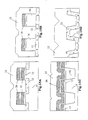
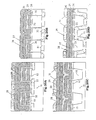
- FIG. 4 A layout diagram of one example of the nonvolatile semiconductor memory device of the present invention is shown in Fig. 4, an X-X' sectional view in a direction (X direction) along the first control gate connected to the column decoder is shown in Fig. 5A, and a Y-Y' sectional view in a direction (Y direction) along the second control gate connected to the row decoder is shown in Fig. 5B.
- reference numeral 2 denotes an impurity diffusion region
- reference numeral 4 the floating gate
- reference numeral 5 a buried oxide film
- reference numeral 6 the ONO stacked layer
- reference numeral 7 the second control gate reference numeral 8 the first control gate
- reference numeral 9 the silicon nitride film.
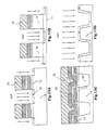
- Fig. 6 The method for fabricating the nonvolatile semiconductor memory device of the present invention will be explained with reference to Fig. 6, and Fig. 7A through Fig. 22A that are sectional views of a line portion in an X1-X1' direction, Fig. 7B through Fig. 22B that are sectional views of a space portion in an X2-X2' direction, Fig. 7C through Fig. 22C that are sectional views of a line portion in a Y1-Y1' direction, and Fig. 7D through Fig. 22D that are sectional views of a space portion in an Y2-Y2' direction.
- a silicon substrate is used as the semiconductor substrate, a tunnel oxide film as the first insulating film, a first polysilicon layer as the floating gate, an ONO film as the second insulating film, a second polysilicon layer as the first control gate, an ONO film as the third insulating film, and a third polysilicon layer as the second control gate.
- a silicon substrate 11 having a first conductivity type is thermally oxidized, and thereby a tunnel oxide film 12 having a film thickness of substantially 10 nm is formed. Thereafter, a first polysilicon layer 13 (film thickness: 50 nm) and a silicon nitride film 14 (film thickness: 250 nm) are sequentially deposited.
- a resist pattern 15 is formed by patterning by use of lithography technology.
- a composite layer of silicon nitride film 14/first polysilicon layer 13/tunnel oxide film 12/silicon substrate 11 is etched out so that an overall etched depth may be 275 nm, thereafter the resist pattern 15 is removed.
- a groove is formed so as to form an STI region.
- the first polysilicon layer 13 runs in a Y direction.
- a silicon oxide film 16 is buried in the groove followed by etching back to completely expose the first polysilicon layer 13.
- a shallow trench isolation region is formed.
- the silicon nitride film 14 is used to protect the floating gate.
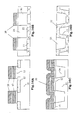
- an ONO film made of a silicon oxide film 17 (film thickness: 4 to 5 nm), a silicon nitride film 18 (5 to 10 nm) and a silicon oxide film 19 (5 to 10 nm) is deposited. Thereafter, a second polysilicon layer 20 is deposited at a film thickness of substantially 50 nm.
- a resist pattern 21 is formed by patterning by means of lithography technology.
- a composite layer of the second polysilicon layer 20/ONO film 19, 18, 17/first polysilicon layer 13/tunnel oxide film 12 is removed by etching.
- the first control gate that runs in a Y direction the same with that of the floating gate is formed.
- the buried silicon oxide film 16 in the shallow trench region is removed by etching, and As + ion implantation is carried out under implantation conditions of 15 keV and 5E14cm -2 .
- the ion implantation is carried out so that diffusion layers may be joined together.
- a bit line 22 is formed.
- an HDP oxide film 23 is deposited at a thickness in the range of 500 to 800 nm.
- the shallow trench region is buried.
- the HDP oxide film 23 is etched back until the silicon substrate 11 is exposed and planarized.
- a silicon oxide film 24 (film thickness: 4 to 5 nm), a silicon nitride film 25 (5 to 10 nm) and a silicon oxide film 26 (5 to 10 nm) are stacked to form an ONO film.
- a third polysilicon layer 27 (150 nm) and a tungsten silicide film 28 (150 nm) are deposited.
- a silicon nitride film 29 is deposited to a film thickness of 10 to 20 nm.
- a resist pattern 30 is formed by patterning by use of lithography technology
- the silicon nitride film 29 is removed by etching.
- a silicon nitride film 31 is deposited to a thickness in the range of from 5 to 10 nm and RIE (Reactive Ion Etching) is performed.
- RIE Reactive Ion Etching
- a sidewall spacer is formed. This is formed to make wider a misalignment margin between a second control gate line and an active region.
- a composite layer of tungsten silicide film 28/third polysilicon layer 27 is removed by etching.
- a second control gate is formed.
- a BPSG (Boron Phosphorus Silicate Glass) protective film 32 is deposited to a film thickness of substantially 1000 nm.
- the writing method, erasing method and reading method of the nonvolatile semiconductor memory device of the present invention will be explained with reference to Fig. 23.
- Operation voltage conditions are shown in Table 1.
- the first control gate is called a control gate (CG) and the second control gate is called a word line (WL).
- CG control gate
- WL word line
- the channel FN phenomenon is utilized.
- the channel FN phenomenon means a phenomenon in which electrons are exchanged between the floating gate and the substrate.
- Cells in a block are in an erase state, that is, all threshold voltages distribute in the range of 4 V or more. Accordingly, in the write operation, only in a cell selected to write, electrons are selectively ejected from the floating gate and thereby lowering the threshold voltage thereof to in the range of 1 V to 2 V. In Fig. 23, a case where a memory cell 20 (M20) is written will be considered.
- a voltage of -15 V is supplied to each of a control gate 2 (CG2) and a word line 0 (WLO).
- CG2 control gate 2
- WLO word line 0
- MBL0 to MBL4 non-selected control gates and non-selected word lines and main bit lines 0 to 4
- 0 V or 0 V floating is supplied, and to each of the substrate and selected gates 0 and 1 (SG0 and SG1), 0 V is supplied.
- a high voltage is applied to a tunnel oxide film between the floating gate and the silicon substrate, and owing to the FN tunnel phenomenon, electrons are ejected from the floating gate into the silicon substrate, resulting in lowering a threshold voltage of the selected cell (M20) to a write state in the range of 1 to 2 V.
- the write operation can be conducted while supplying a positive voltage of +5 V to the substrate at the time of writing.
- a positive voltage of +5 V to the substrate at the time of writing.
- an input write voltage can be lowered (Pgm2 in Table 1).
- 0 V or 0 V floating is supplied, and to the main bit lines 0 to 4 (MBL0 to 4) and the selected gates 0 and 1 (SGO0 and 1), +5 V and +5 V, or 0 V floating and 0 V are supplied, respectively.
- the erase operation here means to inject electrons from the substrate into the floating gate, and thereby raising the threshold voltage to 4 V or more.
- Fig. 23 we consider a case where the erase operation is applied to cells M00, 10, 20, 30, 0n, 1n, 2n and 3n.
- the erase method can be conducted on each bit as the smallest erase range.
- the erase operation can be conducted while supplying a negative voltage of -5 V to the substrate.
- the selected control gate voltage and the selected word line voltage become +10 V, thus the input erase voltage can be lowered.
- -5 V and 0 V, or 0 V floating and -5V are supplied, respectively (Ers2 in Table 1).
- the erase method can be applied on each control gate line as the smallest erase range.
- the erase operation can be conducted while supplying a negative voltage of -8 V to the substrate.
- the selected control gate voltage becomes +15 V
- the input erase voltage can be lowered (Ers4 in Table 1).
- 0 V or 0 V floating is supplied, and to the main bit lines 0 to 4 (MBL0 to MBL4) and the selected gates 0 and 1 (SG0 and SG1), -8 V and 0 V, or 0 V floating and -8 V are supplied, respectively.
- This erase method can be applied on each word line as the minimum erase range.
- the erase operation can be conducted while supplying a negative voltage of -8 V to the substrate.
- the selected word line voltage becomes +15 V
- the input erase voltage can be lowered (Ers6 in Table 1).
- 0 V or 0 V floating is supplied, and to each of the main bit lines 0 to 4 (MBL0 to MBL4) and the selected gates 0 and 1 (SG0 and SG1), -8 V and 0 V, or 0 V floating and -8 V are supplied, respectively.
- either of the electron injection and the electron ejection can select a bit. That is, in the present invention, although the write operation is based on the electron ejection from the substrate to the floating gate and the erase operation is based on the electron injection from the substrate to the floating gate, the erase operation may be based on the electron ejection and the write operation may be based on the electron injection.
- each of the main bit lines MBL1, MBL2 and MBL3 is supplied with 1 V floating
- each of the main bit lines MBL3 and MBL4 is supplied with 0 V
- a voltage of the word line 0 (WL0) is set at +6 V. In this state, whether the selected cell (M20) is in a write state or an erase state is determined on the basis whether or not an electric current flows in the cell (Read2 in Table 1).
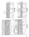
- Fig. 24A an eight cycle read operation in the existing virtual ground array is shown, and in Fig. 24B, a two cycle read operation of the present invention is shown.
- a word line is pre-charged to +3 V and a selected bit line (SBL5) is pre-charged to +1 V (off when it becomes +1 V), and SBL0 and SBL6 to SBL8 are set at 0 V, SBL1, SBL2, SBL4, SBL9 and SBL10 are set at 1 V floating, and SBL3 and SBL11 are set at 1 V, and a read current (Iread) that flows from the selected bit line SBL5 to SBL6 is determined, and thereby the read operation is performed.
- Iread read current
- an eight cycle read operation in which cells on a word line is read divided in eight times is adopted, in addition, in order to inhibit a leakage current from flowing (dotted line 13 in the figure) from a selected bit line 1V (SBL5) to a GND line (SBL0) on a reverse side, a bit line (SBL3) of 1 V force is inserted between the selected bit line 1 V (SBL5) and the GND line (SBL0) on the reverse side.
- the non-selected cells when these are in the write state and the threshold voltage is low, become on-state owing to the word line voltage, an electric current flows from the bit lines (SBL3) of 1 V force (1 V is always applied during the reading) to the selected bit line 1V (SBL5) (dotted arrow mark I1 in the figure), or an electric current flows from the bit lines (SBL3, SBL11) of 1 V force to a GND of common source lines (SBL0, SBL8) (dotted arrow mark I2 in the figure), the common source lines may be set in the floating state, thereby a read cell current may be influenced by other non-selected cells, resulting in deterioration of read accuracy.
- the non-selected cells (M1, M3, M5, M7, M9 and M11) are supplied with a voltage of only substantially 1.5 V.
- the leakage current in a transversal direction is greatly reduced and a two cycle read operation in which the cells on a word line are read divided in two times is realized. Accordingly, read accuracy can be improved and multi-value storage is made easier from the former, and read speed is improved from the latter.
Landscapes
- Engineering & Computer Science (AREA)
- Microelectronics & Electronic Packaging (AREA)
- Power Engineering (AREA)
- Physics & Mathematics (AREA)
- Ceramic Engineering (AREA)
- Condensed Matter Physics & Semiconductors (AREA)
- General Physics & Mathematics (AREA)
- Computer Hardware Design (AREA)
- Non-Volatile Memory (AREA)
- Semiconductor Memories (AREA)
Abstract
Description
| Pgm1 | Pgm2 | Ers1 | Ers2 | Ers3 | Ers4 | Ers5 | Ers6 | Read1 | Read2 | |
| CG0 | 0V/F | 0V/F | +15V | +10V | +30V | +15V | 0V/F | 0V/F | 0V | 0V |
| CG1 | 0V/F | 0V/F | +15V | +10V | +30V | +15V | 0V/F | 0V/F | 0V | 0V |
| CG2 | -15V | -10V | +15V | +10V | +30V | +15V | 0V/F | 0V/F | +3V | 0V |
| CG3 | 0V/F | 0V/F | +15V | +10V | +30V | +15V | 0V/F | 0V/F | 0V | 0V |
| WL0 | -15V | -10V | +15V | +10V | 0V/F | 0V/F | +30V | +15V | +3V | +6V |
| WLn | 0V/F | 0V/F | +15V | +10V | 0V/F | 0V/F | +30V | +15V | 0V | 0V |
| MBL0 | 0V/F | +5V/F | 0V/F | -5V/F | 0V/F | -8V/F | 0V/F | -8V/F | +1V | +1V |
| MBL1 | 0V/F | +5V/F | 0V/F | -5V/F | 0V/F | -8V/F | 0V/F | -8V/F | 0V | +1V |
| MBL2 | 0V/F | +5V/F | 0V/F | -5V/F | 0V/F | -8V/F | 0V/F | -8V/F | +1V | +1V |
| MBL3 | 0V/F | +5V/F | 0V/F | -5V/F | 0V/F | -8V/F | 0V/F | -8V/F | 0V | 0V |
| MBL4 | 0V/F | +5V/F | 0V/F | -5V/F | 0V/F | -8V/F | 0V/F | -8V/F | +1V | 0V |
| Sub | 0V | +5V | 0V | -5V | 0V | -8V | 0V | -8V | 0V | 0V |
| SG0 | 0V | +5/0V | 0V | 0V/-5V | 0V | 0V/-8V | 0V | 0V/-8V | +3V | +3V |
| SG1 | 0V | +5/0V | 0V | 0V/-5V | 0V | 0V/-8V | 0V | 0V/-8V | +3V | +3V |
| (F=0V floating ) |
Claims (20)
- A nonvolatile semiconductor memory device comprising a cell which includes:a drain diffusion region and a source diffusion region formed on a surface layer of a semiconductor substrate;a first insulating film formed between the source diffusion region and the drain diffusion region;a floating gate formed on the first insulating film;a second insulating film formed on the floating gate;a first control gate formed on the second insulating film;a third insulating film formed on the first control gate and a sidewall thereof and on a sidewall of the floating gate; anda second control gate formed on the first control gate with the third insulating film interposed therebetween.
- A nonvolatile semiconductor memory device according to claim 1, wherein the first control gate and the second control gate are connected to a column decoder and a row decoder, respectively, and the floating gate is capacitively coupled to the first control gate and the second control gate.
- A nonvolatile semiconductor memory device according to claim 1, wherein the drain diffusion region and the source diffusion region have structures symmetric to each other.
- A nonvolatile semiconductor memory device according to claim 1 comprising a plurality of cells in a channel length direction, wherein a source diffusion region of one cell and a drain diffusion region of another cell adjacent to said one cell in the channel length direction are shared in common as one bit line.
- A nonvolatile semiconductor memory device according to claim 4 comprising a plurality of cells in the channel length direction and in a channel width direction, wherein first control gates of a line of cells continuous in the channel length or width direction are shared in common as one first control gate line, and second control gates of a line of cells continuous in a direction perpendicular to the first control gate line are shared in common as one second control gate line.
- A method for fabricating a nonvolatile semiconductor memory device comprising formation of a cell, the formation of the cell comprising the steps of:(a) stacking a first insulating film and a first conductor film in this order on a semiconductor substrate and forming a floating gate by processing the first conductor film;(b) stacking a second insulating film and a second conductor film in this order on the floating gate and forming a first control gate by processing the second conductor film;(c) implanting an impurity, with the first control gate as a mask, in a surface layer of the semiconductor substrate, thereby forming a drain diffusion region and a source diffusion region;(d) forming a third insulating film on the first control gate and a sidewall thereof and on a sidewall of the floating gate; and(e) stacking a third conductor film on the third insulating film and, by processing the third conductor film, forming a second control gate on the first control gate with the third insulating film interposed therebetween.
- A method for fabricating a nonvolatile semiconductor memory device according to claim 6, wherein the second insulating film and/or the third insulating film are/is formed of an ONO film.
- A method for fabricating a nonvolatile semiconductor memory device according to claim 6, wherein the nonvolatile semiconductor memory device includes a plurality of cells in a channel width direction, and the method further comprises, after the step (a) and before the step (b), the step of forming an element isolation region in the semiconductor substrate between the floating gates by means of a STI method, and after the step (b) and before the step (c), the step of removing the element isolation region partially so that a source diffusion region and a drain diffusion region of adjacent cells are shared in common as one bit line.
- A method for fabricating a nonvolatile semiconductor memory device according to claim 6, wherein the processing of the third conductor film into the second control gate is performed by use of a mask provided with a sidewall spacer.
- A writing method for a nonvolatile semiconductor memory device as set forth in claim 5, comprising supplying a predetermined positive voltage to the first control gate line and the second control gate line of a selected cell and grounding the semiconductor substrate, thereby injecting electrons from the semiconductor substrate into the floating gate of the selected cell for conducting a writing operation, or supplying a predetermined negative voltage to the first control gate line and the second control gate line of the selected cell and grounding the semiconductor substrate, thereby injecting electrons from the floating gate of the selected cell into the semiconductor substrate for conducting a writing operation.
- A writing method for a nonvolatile semiconductor memory device as set forth in claim 5, comprising supplying a predetermined positive voltage to the first control gate line and the second control gate line of a selected cell, supplying a voltage lower than the above positive voltage to the semiconductor substrate and supplying a voltage substantially the same as the voltage to the semiconductor substrate to a bit line of the selected cell or disconnecting the bit line, thereby injecting electrons from the semiconductor substrate into the floating gate of the selected cell for conducting a write operation, or supplying a predetermined negative voltage to the first control gate line and the second control gate line of the selected cell, supplying a voltage higher than the above negative voltage to the semiconductor substrate and supplying a voltage substantially the same as the voltage to the semiconductor substrate to a bit line of the selected cell or disconnecting the bit line, thereby injecting electrons from the floating gate of the selected cell into the semiconductor substrate for conducting a write operation.
- An erasing method for a nonvolatile semiconductor memory device as set forth in claim 5, comprising supplying a predetermined negative voltage to the first control gate line of a selected cell and grounding the semiconductor substrate, thereby injecting electrons from the floating gate of the selected cell into the semiconductor substrate for conducting an erase operation, or supplying a predetermined positive voltage to the first control gate line of the selected cell and grounding the semiconductor substrate, thereby injecting electrons from the semiconductor substrate into the floating gate of the selected cell for conducting an erase operation.
- An erasing method for a nonvolatile semiconductor memory device as set forth in claim 5, comprising supplying a predetermined negative voltage to the first control gate line of a selected cell, supplying a voltage higher than the above negative voltage to the semiconductor substrate and supplying a voltage substantially the same as the voltage to the semiconductor substrate to a bit line of the selected cell or disconnecting the bit line, thereby injecting electrons from the floating gate of the selected cell into the semiconductor substrate for conducting an erase operation, or supplying a predetermined positive voltage to the first control gate line of the selected cell, supplying a voltage lower than the above positive voltage to the semiconductor substrate and supplying a voltage substantially the same as the voltage to the semiconductor substrate to a bit line of the selected cell or disconnecting the bit line, thereby injecting electrons from the semiconductor substrate into the floating gate of the selected cell for conducting an erase operation.
- An erasing method for a nonvolatile semiconductor memory device as set forth in claim 5, comprising supplying a predetermined negative voltage to the second control gate line of a selected cell and grounding the semiconductor substrate, thereby injecting electrons from the floating gate of the selected cell into the semiconductor substrate for conducting an erase operation, or supplying a predetermined positive voltage to the second control gate line of the selected cell and grounding the semiconductor substrate, thereby injecting electrons from the semiconductor substrate into the floating gate of the selected cell for conducting an erase operation.
- An erasing method for a nonvolatile semiconductor memory device as set forth in claim 5, comprising supplying a predetermined negative voltage to the second control gate line of a selected cell, supplying a voltage higher than the above negative voltage to the semiconductor substrate and supplying a voltage substantially the same as the voltage to the semiconductor substrate to a bit line of the selected cell or disconnecting the bit line, thereby injecting electrons from the floating gate of the selected cell into the semiconductor substrate for conducting an. erase operation, or supplying a predetermined positive voltage to the second control gate line of the selected cell, supplying a voltage lower than the above positive voltage to the semiconductor substrate and supplying a voltage substantially the same as the voltage to the semiconductor substrate to a bit line of the selected cell or disconnecting the bit line, thereby injecting electrons from the semiconductor substrate into the floating gate of the selected cell for conducting an erase operation.
- An erasing method for a nonvolatile semiconductor memory device as set forth in claim 5, comprising supplying a predetermined negative voltage to the first control gate line and the second control gate line of a selected cell and grounding the semiconductor substrate, thereby injecting electrons from the floating gate of the selected cell into the semiconductor substrate for conducting an erase operation, or supplying a predetermined positive voltage to the first control gate line and the second control gate line of the selected cell and grounding the semiconductor substrate, thereby injecting electrons from the semiconductor substrate into the floating gate of the selected cell for conducting an erase operation.
- An erasing method for a nonvolatile semiconductor memory device as set forth in claim 5, comprising supplying a predetermined negative voltage to the first control gate line and the second control gate line of a selected cell, supplying a voltage higher than the above negative voltage to the semiconductor substrate and supplying a voltage substantially the same as the voltage to the semiconductor substrate to a bit line of the selected cell or disconnecting the bit line, thereby injecting electrons from the floating gate of the selected cell into the semiconductor substrate for conducting an erase operation, or supplying a predetermined positive voltage to the first control gate line and the second control gate line of the selected cell, supplying a voltage lower than the above positive voltage to the semiconductor substrate, and supplying a voltage substantially the same as the voltage to the semiconductor substrate to a bit line of the selected cell or disconnecting the bit line, thereby injecting electrons from the semiconductor substrate into the floating gate of the selected cell for conducting an erase operation.
- A reading method for a nonvolatile semiconductor memory device as set forth in claim 5, comprising supplying a predetermined positive voltage to the second control gate line of a selected cell and a bit line corresponding to the source diffusion region of the selected cell and grounding a bit line corresponding to the drain diffusion region of the selected cell, thereby conducting a reading operation.
- A reading method for a nonvolatile semiconductor memory device as set forth in claim 5, comprising supplying a predetermined positive voltage to the first control gate line and the second control gate line of a selected cell and a bit line corresponding to the source diffusion region of the selected cell and grounding a bit line corresponding to the drain diffusion region of the selected cell, thereby conducting a reading operation.
- A reading method for a nonvolatile semiconductor memory device as set forth in claim 5, comprising supplying a predetermined positive voltage to the second control gate lines of selected cells, supplying a positive voltage to odd-numbered first control gate lines and bit lines corresponding to odd-numbered drain diffusion regions and grounding even-numbered first control gate lines and bit lines corresponding to even-numbered source diffusion regions, thereby reading odd-numbered cells of the selected cells, and subsequently, while supplying the predetermined positive voltage to the second control gate lines of the selected cells, supplying a positive voltage to even-numbered first control gate lines and bit lines corresponding to even-numbered drain diffusion regions and grounding odd-numbered first control gate lines and bit lines corresponding to odd-numbered source diffusion regions, thereby reading even-numbered ones of the selected cells.
Applications Claiming Priority (2)
| Application Number | Priority Date | Filing Date | Title |
|---|---|---|---|
| JP2001264158 | 2001-08-31 | ||
| JP2001264158A JP4065671B2 (en) | 2001-08-31 | 2001-08-31 | Nonvolatile semiconductor memory device, manufacturing method thereof, and operation method thereof |
Publications (2)
| Publication Number | Publication Date |
|---|---|
| EP1289023A2 true EP1289023A2 (en) | 2003-03-05 |
| EP1289023A3 EP1289023A3 (en) | 2007-11-14 |
Family
ID=19090808
Family Applications (1)
| Application Number | Title | Priority Date | Filing Date |
|---|---|---|---|
| EP02019493A Withdrawn EP1289023A3 (en) | 2001-08-31 | 2002-08-30 | Nonvolatile semiconductor memory device, fabricating method thereof and operation method thereof |
Country Status (6)
| Country | Link |
|---|---|
| US (1) | US7187029B2 (en) |
| EP (1) | EP1289023A3 (en) |
| JP (1) | JP4065671B2 (en) |
| KR (1) | KR100495892B1 (en) |
| CN (1) | CN1244156C (en) |
| TW (1) | TW560011B (en) |
Cited By (2)
| Publication number | Priority date | Publication date | Assignee | Title |
|---|---|---|---|---|
| WO2004040583A1 (en) * | 2002-10-28 | 2004-05-13 | Sandisk Corporation | Flash memory cell arrays having dual control gates per memory cell charge storage element |
| US7951669B2 (en) | 2006-04-13 | 2011-05-31 | Sandisk Corporation | Methods of making flash memory cell arrays having dual control gates per memory cell charge storage element |
Families Citing this family (9)
| Publication number | Priority date | Publication date | Assignee | Title |
|---|---|---|---|---|
| US20040197992A1 (en) * | 2003-04-03 | 2004-10-07 | Hsiao-Ying Yang | Floating gates having improved coupling ratios and fabrication method thereof |
| JP3762385B2 (en) | 2003-04-28 | 2006-04-05 | 株式会社東芝 | Nonvolatile semiconductor memory device |
| US8022489B2 (en) * | 2005-05-20 | 2011-09-20 | Macronix International Co., Ltd. | Air tunnel floating gate memory cell |
| JP4936790B2 (en) * | 2006-05-22 | 2012-05-23 | 株式会社東芝 | Semiconductor device |
| JP4908238B2 (en) * | 2007-01-11 | 2012-04-04 | 株式会社東芝 | Nonvolatile semiconductor memory device |
| KR20100080243A (en) * | 2008-12-31 | 2010-07-08 | 주식회사 동부하이텍 | Semiconductor device and fabricating method thereof |
| US8692310B2 (en) | 2009-02-09 | 2014-04-08 | Spansion Llc | Gate fringing effect based channel formation for semiconductor device |
| WO2011145676A1 (en) * | 2010-05-20 | 2011-11-24 | シャープ株式会社 | Display device with touch sensor |
| US9337099B1 (en) | 2015-01-30 | 2016-05-10 | Globalfoundries Inc. | Special constructs for continuous non-uniform active region FinFET standard cells |
Citations (4)
| Publication number | Priority date | Publication date | Assignee | Title |
|---|---|---|---|---|
| EP0138439A2 (en) * | 1983-09-28 | 1985-04-24 | Kabushiki Kaisha Toshiba | Electrically erasable programable nonvolatile semiconductor memory device having dual-control gate |
| US5280446A (en) * | 1990-09-20 | 1994-01-18 | Bright Microelectronics, Inc. | Flash eprom memory circuit having source side programming |
| US5518943A (en) * | 1993-12-16 | 1996-05-21 | Kabushiki Kaisha Toshiba | Method of manufacturing nonvolatile semiconductor memory device having an implanted damage layer |
| US5910915A (en) * | 1992-01-14 | 1999-06-08 | Sandisk Corporation | EEPROM with split gate source side injection |
Family Cites Families (12)
| Publication number | Priority date | Publication date | Assignee | Title |
|---|---|---|---|---|
| US4599706A (en) * | 1985-05-14 | 1986-07-08 | Xicor, Inc. | Nonvolatile electrically alterable memory |
| JP3671432B2 (en) | 1994-05-17 | 2005-07-13 | ソニー株式会社 | Nonvolatile memory and manufacturing method thereof |
| US5429971A (en) * | 1994-10-03 | 1995-07-04 | United Microelectronics Corporation | Method of making single bit erase flash EEPROM |
| JP3123921B2 (en) * | 1995-05-18 | 2001-01-15 | 三洋電機株式会社 | Semiconductor device and nonvolatile semiconductor memory |
| US5877054A (en) | 1995-06-29 | 1999-03-02 | Sharp Kabushiki Kaisha | Method of making nonvolatile semiconductor memory |
| JP3081543B2 (en) * | 1996-03-29 | 2000-08-28 | 三洋電機株式会社 | Split gate transistor, method of manufacturing split gate transistor, and nonvolatile semiconductor memory |
| JP3123924B2 (en) * | 1996-06-06 | 2001-01-15 | 三洋電機株式会社 | Non-volatile semiconductor memory |
| KR100215883B1 (en) * | 1996-09-02 | 1999-08-16 | 구본준 | A flash memory device and manufacturing method thereof |
| JPH11224940A (en) * | 1997-12-05 | 1999-08-17 | Sony Corp | Nonvolatile semiconductor memory device and writing method therefor |
| US5991225A (en) * | 1998-02-27 | 1999-11-23 | Micron Technology, Inc. | Programmable memory address decode array with vertical transistors |
| KR20000027275A (en) * | 1998-10-27 | 2000-05-15 | 김영환 | Flash memory cell and method for manufacturing the same |
| US6154018A (en) * | 1999-09-01 | 2000-11-28 | Vlsi Technology, Inc. | High differential impedance load device |
-
2001
- 2001-08-31 JP JP2001264158A patent/JP4065671B2/en not_active Expired - Fee Related
-
2002
- 2002-08-26 KR KR10-2002-0050576A patent/KR100495892B1/en active IP Right Grant
- 2002-08-29 US US10/230,369 patent/US7187029B2/en not_active Expired - Lifetime
- 2002-08-30 EP EP02019493A patent/EP1289023A3/en not_active Withdrawn
- 2002-08-30 TW TW091119894A patent/TW560011B/en not_active IP Right Cessation
- 2002-09-02 CN CNB021416117A patent/CN1244156C/en not_active Expired - Lifetime
Patent Citations (4)
| Publication number | Priority date | Publication date | Assignee | Title |
|---|---|---|---|---|
| EP0138439A2 (en) * | 1983-09-28 | 1985-04-24 | Kabushiki Kaisha Toshiba | Electrically erasable programable nonvolatile semiconductor memory device having dual-control gate |
| US5280446A (en) * | 1990-09-20 | 1994-01-18 | Bright Microelectronics, Inc. | Flash eprom memory circuit having source side programming |
| US5910915A (en) * | 1992-01-14 | 1999-06-08 | Sandisk Corporation | EEPROM with split gate source side injection |
| US5518943A (en) * | 1993-12-16 | 1996-05-21 | Kabushiki Kaisha Toshiba | Method of manufacturing nonvolatile semiconductor memory device having an implanted damage layer |
Cited By (10)
| Publication number | Priority date | Publication date | Assignee | Title |
|---|---|---|---|---|
| WO2004040583A1 (en) * | 2002-10-28 | 2004-05-13 | Sandisk Corporation | Flash memory cell arrays having dual control gates per memory cell charge storage element |
| US6888755B2 (en) | 2002-10-28 | 2005-05-03 | Sandisk Corporation | Flash memory cell arrays having dual control gates per memory cell charge storage element |
| US7075823B2 (en) | 2002-10-28 | 2006-07-11 | Sandisk Corporation | Flash memory cell arrays having dual control gates per memory cell charge storage element |
| US7303956B2 (en) | 2002-10-28 | 2007-12-04 | Sandisk Corporation | Flash memory cell arrays having dual control gates per memory cell charge storage element |
| US7486555B2 (en) | 2002-10-28 | 2009-02-03 | Sandisk Corporation | Flash memory cell arrays having dual control gates per memory cell charge storage element |
| US7502261B2 (en) | 2002-10-28 | 2009-03-10 | Sandisk Corporation | Flash memory cell arrays having dual control gates per memory cell charge storage element |
| US7638834B2 (en) | 2002-10-28 | 2009-12-29 | Sandisk Corporation | Flash memory cell arrays having dual control gates per memory cell charge storage element |
| US7994004B2 (en) | 2002-10-28 | 2011-08-09 | Sandisk Technologies Inc. | Flash memory cell arrays having dual control gates per memory cell charge storage element |
| US8334180B2 (en) | 2002-10-28 | 2012-12-18 | Sandisk Technologies Inc | Flash memory cell arrays having dual control gates per memory cell charge storage element |
| US7951669B2 (en) | 2006-04-13 | 2011-05-31 | Sandisk Corporation | Methods of making flash memory cell arrays having dual control gates per memory cell charge storage element |
Also Published As
| Publication number | Publication date |
|---|---|
| EP1289023A3 (en) | 2007-11-14 |
| CN1244156C (en) | 2006-03-01 |
| US7187029B2 (en) | 2007-03-06 |
| JP2003078042A (en) | 2003-03-14 |
| KR20030019111A (en) | 2003-03-06 |
| TW560011B (en) | 2003-11-01 |
| US20030047774A1 (en) | 2003-03-13 |
| KR100495892B1 (en) | 2005-06-16 |
| CN1404152A (en) | 2003-03-19 |
| JP4065671B2 (en) | 2008-03-26 |
Similar Documents
| Publication | Publication Date | Title |
|---|---|---|
| KR100506445B1 (en) | Semiconductor device and manufacturing method thereof | |
| KR100436673B1 (en) | Semiconductor device and manufacturing method thereof | |
| US5939749A (en) | Split gate transistor array | |
| US7315056B2 (en) | Semiconductor memory array of floating gate memory cells with program/erase and select gates | |
| US6531732B2 (en) | Nonvolatile semiconductor memory device, process of manufacturing the same and method of operating the same | |
| US5877054A (en) | Method of making nonvolatile semiconductor memory | |
| JPH10223867A (en) | Semiconductor device and manufacture thereof | |
| JPH0567791A (en) | Electrically writable and erasable semiconductor memory device and its manufacture | |
| US20100172178A1 (en) | Semiconductor device manufacturing method and semiconductor integrated circuit device | |
| US20100283099A1 (en) | Non-Volatile Semiconductor Memory Device and Manufacturing Method Thereof | |
| US7187029B2 (en) | Nonvolatile semiconductor memory device with floating gate and two control gates | |
| US6493264B2 (en) | Nonvolatile semiconductor memory, method of reading from and writing to the same and method of manufacturing the same | |
| JP4461042B2 (en) | Method for manufacturing nonvolatile memory | |
| JP2007142468A (en) | Semiconductor device | |
| US20020055228A1 (en) | Sidewall process to improve the flash memory cell performance | |
| JP2001284473A (en) | Nonvolatile semiconductor memory | |
| JP2007201244A (en) | Semiconductor device | |
| JP3947041B2 (en) | Semiconductor device and manufacturing method thereof | |
| USRE37199E1 (en) | Method of making nonvolatile semiconductor memory | |
| US6392927B2 (en) | Cell array, operating method of the same and manufacturing method of the same | |
| JP3198682B2 (en) | Manufacturing method of nonvolatile semiconductor memory device | |
| JP4521253B2 (en) | Manufacturing method of semiconductor memory device | |
| JPH11260941A (en) | Transistor, transistor array, manufacture of transistor array and non-volatile semiconductor memory | |
| JP2003347439A (en) | Semiconductor memory | |
| JP2001057397A (en) | Semiconductor memory and operating method of the same |
Legal Events
| Date | Code | Title | Description |
|---|---|---|---|
| PUAI | Public reference made under article 153(3) epc to a published international application that has entered the european phase |
Free format text: ORIGINAL CODE: 0009012 |
|
| AK | Designated contracting states |
Kind code of ref document: A2 Designated state(s): AT BE BG CH CY CZ DE DK EE ES FI FR GB GR IE IT LI LU MC NL PT SE SK TR Designated state(s): AT BE BG CH CY CZ DE DK EE ES FI FR GB GR IE IT LI LU MC NL PT SE SK TR |
|
| AX | Request for extension of the european patent |
Extension state: AL LT LV MK RO SI |
|
| PUAL | Search report despatched |
Free format text: ORIGINAL CODE: 0009013 |
|
| AK | Designated contracting states |
Kind code of ref document: A3 Designated state(s): AT BE BG CH CY CZ DE DK EE ES FI FR GB GR IE IT LI LU MC NL PT SE SK TR |
|
| AX | Request for extension of the european patent |
Extension state: AL LT LV MK RO SI |
|
| 17P | Request for examination filed |
Effective date: 20080320 |
|
| AKX | Designation fees paid |
Designated state(s): DE FR GB |
|
| 17Q | First examination report despatched |
Effective date: 20090316 |
|
| STAA | Information on the status of an ep patent application or granted ep patent |
Free format text: STATUS: THE APPLICATION IS DEEMED TO BE WITHDRAWN |
|
| 18D | Application deemed to be withdrawn |
Effective date: 20090728 |