EP1291904A2 - GaN substrate formed over GaN layer having discretely formed minute holes produced by selective growth - Google Patents
GaN substrate formed over GaN layer having discretely formed minute holes produced by selective growth Download PDFInfo
- Publication number
- EP1291904A2 EP1291904A2 EP02019861A EP02019861A EP1291904A2 EP 1291904 A2 EP1291904 A2 EP 1291904A2 EP 02019861 A EP02019861 A EP 02019861A EP 02019861 A EP02019861 A EP 02019861A EP 1291904 A2 EP1291904 A2 EP 1291904A2
- Authority
- EP
- European Patent Office
- Prior art keywords
- substrate
- gan layer
- mask
- gan
- layers
- Prior art date
- Legal status (The legal status is an assumption and is not a legal conclusion. Google has not performed a legal analysis and makes no representation as to the accuracy of the status listed.)
- Withdrawn
Links
Images


Classifications
-
- C—CHEMISTRY; METALLURGY
- C30—CRYSTAL GROWTH
- C30B—SINGLE-CRYSTAL GROWTH; UNIDIRECTIONAL SOLIDIFICATION OF EUTECTIC MATERIAL OR UNIDIRECTIONAL DEMIXING OF EUTECTOID MATERIAL; REFINING BY ZONE-MELTING OF MATERIAL; PRODUCTION OF A HOMOGENEOUS POLYCRYSTALLINE MATERIAL WITH DEFINED STRUCTURE; SINGLE CRYSTALS OR HOMOGENEOUS POLYCRYSTALLINE MATERIAL WITH DEFINED STRUCTURE; AFTER-TREATMENT OF SINGLE CRYSTALS OR A HOMOGENEOUS POLYCRYSTALLINE MATERIAL WITH DEFINED STRUCTURE; APPARATUS THEREFOR
- C30B25/00—Single-crystal growth by chemical reaction of reactive gases, e.g. chemical vapour-deposition growth
- C30B25/02—Epitaxial-layer growth
- C30B25/18—Epitaxial-layer growth characterised by the substrate
-
- C—CHEMISTRY; METALLURGY
- C30—CRYSTAL GROWTH
- C30B—SINGLE-CRYSTAL GROWTH; UNIDIRECTIONAL SOLIDIFICATION OF EUTECTIC MATERIAL OR UNIDIRECTIONAL DEMIXING OF EUTECTOID MATERIAL; REFINING BY ZONE-MELTING OF MATERIAL; PRODUCTION OF A HOMOGENEOUS POLYCRYSTALLINE MATERIAL WITH DEFINED STRUCTURE; SINGLE CRYSTALS OR HOMOGENEOUS POLYCRYSTALLINE MATERIAL WITH DEFINED STRUCTURE; AFTER-TREATMENT OF SINGLE CRYSTALS OR A HOMOGENEOUS POLYCRYSTALLINE MATERIAL WITH DEFINED STRUCTURE; APPARATUS THEREFOR
- C30B29/00—Single crystals or homogeneous polycrystalline material with defined structure characterised by the material or by their shape
- C30B29/10—Inorganic compounds or compositions
- C30B29/40—AIIIBV compounds wherein A is B, Al, Ga, In or Tl and B is N, P, As, Sb or Bi
- C30B29/403—AIII-nitrides
- C30B29/406—Gallium nitride
-
- H—ELECTRICITY
- H01—ELECTRIC ELEMENTS
- H01L—SEMICONDUCTOR DEVICES NOT COVERED BY CLASS H10
- H01L21/00—Processes or apparatus adapted for the manufacture or treatment of semiconductor or solid state devices or of parts thereof
- H01L21/02—Manufacture or treatment of semiconductor devices or of parts thereof
- H01L21/02104—Forming layers
- H01L21/02365—Forming inorganic semiconducting materials on a substrate
- H01L21/02367—Substrates
- H01L21/0237—Materials
-
- H—ELECTRICITY
- H01—ELECTRIC ELEMENTS
- H01L—SEMICONDUCTOR DEVICES NOT COVERED BY CLASS H10
- H01L21/00—Processes or apparatus adapted for the manufacture or treatment of semiconductor or solid state devices or of parts thereof
- H01L21/02—Manufacture or treatment of semiconductor devices or of parts thereof
- H01L21/02104—Forming layers
- H01L21/02365—Forming inorganic semiconducting materials on a substrate
- H01L21/02436—Intermediate layers between substrates and deposited layers
- H01L21/02439—Materials
- H01L21/02455—Group 13/15 materials
- H01L21/02458—Nitrides
-
- H—ELECTRICITY
- H01—ELECTRIC ELEMENTS
- H01L—SEMICONDUCTOR DEVICES NOT COVERED BY CLASS H10
- H01L21/00—Processes or apparatus adapted for the manufacture or treatment of semiconductor or solid state devices or of parts thereof
- H01L21/02—Manufacture or treatment of semiconductor devices or of parts thereof
- H01L21/02104—Forming layers
- H01L21/02365—Forming inorganic semiconducting materials on a substrate
- H01L21/02518—Deposited layers
- H01L21/02521—Materials
- H01L21/02538—Group 13/15 materials
- H01L21/0254—Nitrides
-
- H—ELECTRICITY
- H01—ELECTRIC ELEMENTS
- H01L—SEMICONDUCTOR DEVICES NOT COVERED BY CLASS H10
- H01L21/00—Processes or apparatus adapted for the manufacture or treatment of semiconductor or solid state devices or of parts thereof
- H01L21/02—Manufacture or treatment of semiconductor devices or of parts thereof
- H01L21/02104—Forming layers
- H01L21/02365—Forming inorganic semiconducting materials on a substrate
- H01L21/02518—Deposited layers
- H01L21/0257—Doping during depositing
- H01L21/02573—Conductivity type
- H01L21/02576—N-type
-
- H—ELECTRICITY
- H01—ELECTRIC ELEMENTS
- H01L—SEMICONDUCTOR DEVICES NOT COVERED BY CLASS H10
- H01L21/00—Processes or apparatus adapted for the manufacture or treatment of semiconductor or solid state devices or of parts thereof
- H01L21/02—Manufacture or treatment of semiconductor devices or of parts thereof
- H01L21/02104—Forming layers
- H01L21/02365—Forming inorganic semiconducting materials on a substrate
- H01L21/02518—Deposited layers
- H01L21/0257—Doping during depositing
- H01L21/02573—Conductivity type
- H01L21/02579—P-type
-
- H—ELECTRICITY
- H01—ELECTRIC ELEMENTS
- H01L—SEMICONDUCTOR DEVICES NOT COVERED BY CLASS H10
- H01L21/00—Processes or apparatus adapted for the manufacture or treatment of semiconductor or solid state devices or of parts thereof
- H01L21/02—Manufacture or treatment of semiconductor devices or of parts thereof
- H01L21/02104—Forming layers
- H01L21/02365—Forming inorganic semiconducting materials on a substrate
- H01L21/02612—Formation types
- H01L21/02617—Deposition types
- H01L21/0262—Reduction or decomposition of gaseous compounds, e.g. CVD
-
- H—ELECTRICITY
- H01—ELECTRIC ELEMENTS
- H01L—SEMICONDUCTOR DEVICES NOT COVERED BY CLASS H10
- H01L21/00—Processes or apparatus adapted for the manufacture or treatment of semiconductor or solid state devices or of parts thereof
- H01L21/02—Manufacture or treatment of semiconductor devices or of parts thereof
- H01L21/02104—Forming layers
- H01L21/02365—Forming inorganic semiconducting materials on a substrate
- H01L21/02612—Formation types
- H01L21/02617—Deposition types
- H01L21/02636—Selective deposition, e.g. simultaneous growth of mono- and non-monocrystalline semiconductor materials
- H01L21/02639—Preparation of substrate for selective deposition
-
- H—ELECTRICITY
- H01—ELECTRIC ELEMENTS
- H01L—SEMICONDUCTOR DEVICES NOT COVERED BY CLASS H10
- H01L21/00—Processes or apparatus adapted for the manufacture or treatment of semiconductor or solid state devices or of parts thereof
- H01L21/02—Manufacture or treatment of semiconductor devices or of parts thereof
- H01L21/02104—Forming layers
- H01L21/02365—Forming inorganic semiconducting materials on a substrate
- H01L21/02612—Formation types
- H01L21/02617—Deposition types
- H01L21/02636—Selective deposition, e.g. simultaneous growth of mono- and non-monocrystalline semiconductor materials
- H01L21/02647—Lateral overgrowth
-
- H—ELECTRICITY
- H01—ELECTRIC ELEMENTS
- H01L—SEMICONDUCTOR DEVICES NOT COVERED BY CLASS H10
- H01L33/00—Semiconductor devices with at least one potential-jump barrier or surface barrier specially adapted for light emission; Processes or apparatus specially adapted for the manufacture or treatment thereof or of parts thereof; Details thereof
- H01L33/005—Processes
- H01L33/0062—Processes for devices with an active region comprising only III-V compounds
- H01L33/0066—Processes for devices with an active region comprising only III-V compounds with a substrate not being a III-V compound
- H01L33/007—Processes for devices with an active region comprising only III-V compounds with a substrate not being a III-V compound comprising nitride compounds
Definitions
- the present invention relates to a substrate which is used in a semiconductor element.
- the present invention also relates to a process for producing a substrate which is used in a semiconductor element.
- the present invention further relates to a semiconductor element which uses the above substrate.
- Japanese Journal of Applied Physics Vol. 37 (1998) Part 2, pp. L1020 discloses a short-wavelength semiconductor laser device which emits laser light in the 410 nm band.
- This semiconductor laser device is produced as follows. First, a GaN layer is formed on a sapphire substrate, a stripe pattern of a SiO 2 film is formed on the GaN layer, and a GaN thick film is formed by selective lateral growth from nuclei of the growth generated in stripe areas of the GaN layer which are not covered by the stripe pattern of the SiO 2 mask. Then, a GaN substrate is obtained by separating the GaN thick film from the sapphire substrate.
- the highest output power obtained in the fundamental transverse mode by the above semiconductor laser devices is about 30 mW, and the semiconductor laser device is reliable in the output power range up to 30 mW.
- the conventional ELOG (epitaxial lateral overgrowth) substrates as above are produced by selective lateral growth from nuclei of the growth generated in stripe areas of a GaN layer which are not covered by SiO 2 mask, defects are reduced in the region produced by the selective lateral growth of GaN.
- the density of the nuclei for growth is high, and therefore the spaces between the nuclei are bridged before the grown nuclei become large. Thus, defects are likely to be produced in the bridged regions.
- the GaN thick film is required to have a certain thickness in order to use the GaN thick film as a substrate, the defect density is increased with increase in the thickness. Even when the defect densities in the bridged regions are low, the defect density increases with the increase in the thickness, Consequently, it is difficult to form a wide low-defect region. That is, the conventional ELOG substrates have only a small low-defect region.
- the conventional ELOG substrates are effective for producing semiconductor laser devices having a narrow stripe structure as disclosed in the aforementioned reference.
- the semiconductor laser device In order to realize a reliable semiconductor laser device having high output power, the semiconductor laser device is required to have a broad stripe structure, and in order to realize a reliable semiconductor laser device having a broad stripe structure, the semiconductor laser device is required to be formed on a GaN substrate which includes a wide low-defect region, instead of the conventional ELOG substrates.
- An object of the present invention is to provide a substrate which is used in a semiconductor element, and in which the defect density is low in a wide region.
- Another object of the present invention is to provide process for producing a substrate which is used in a semiconductor element, and in which the defect density is low in a wide region.
- a further object of the present invention is to provide a semiconductor element which uses a substrate in which the defect density is low in a wide region.
- a (first) growth suppression mask which is constituted by a plurality of (first) mask elements being discretely arranged and each having a width of 2.5 micrometers or smaller is formed on a surface of a base substrate; a first GaN layer having a plurality of holes is formed on the surface of the base substrate by growing GaN from areas of the surface of the base substrate which are not covered by the plurality of first mask elements; and a second GaN layer is formed over the first GaN layer by crystal growth. Therefore, the density of the nuclei of growth can be reduced compared with the conventional process. Thus, it is possible to obtain a GaN layer having a wide low-defect region, and the obtained GaN layer can be used as a reliable substrate.
- the first GaN layer having a plurality of holes is formed by forming on a base surface a growth suppression mask constituted by a plurality of mask elements being discretely arranged and each having a width of 2.5 micrometers or smaller, and growing GaN from areas of the base surface which are not covered by the plurality of mask elements, the formation of the first GaN layer having the plurality of holes according to the present invention is easier than other formation processes, for example, a process in which a GaN layer having a plurality of holes is formed by first forming a GaN layer which has no holes, and then producing holes by etching or the like.
- the diameters of the plurality of holes formed in the first GaN layer are equivalent to the diameters of the plurality of mask elements constituting the growth suppression mask, and the plurality of holes formed in the first GaN layer occupy approximately 40 to 90% of the entire area of the first GaN layer. Therefore, when the second GaN layer is formed over the first GaN layer as above, the nuclei of growth can be effectively reduced. Thus, it is possible to obtain a GaN layer having low defect density.
- a conductive GaN layer is formed as an uppermost layer of the substrate, it is possible to obtain a conductive GaN layer having low defect density.
- the semiconductor element according to the ninth aspect of the present invention is realized by forming semiconductor layers on one of the substrates according to the present invention, reliability of the semiconductor elements is high.
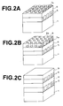
- Figs. 1A to 1D are diagrammatic perspective views of structures in representative stages of a process for producing a substrate for use in a semiconductor element in the first embodiment of the present invention, where Fig. 1D shows the completed structure of the substrate as the first embodiment.
- the substrate for use in a semiconductor element comprises a base substrate 1, a first GaN layer 5 formed on the base substrate 1, and a second GaN layer 6 formed over the first GaN layer 5 by crystal growth, where a plurality of holes 5b are formed in the first GaN layer 5.
- the substrate as the first embodiment is produced as follows.
- a SiO 2 film 4 is formed on the base substrate 1 as illustrated in Fig. 1A, and then a growth suppression mask 4a constituted by a plurality of dot-like (disk-like) mask elements made of SiO 2 are formed on the base substrate 1, where the plurality of dot-like (disk-like) mask elements are discretely arranged on the upper surface of the base substrate 1 as illustrated in Fig. 1B.
- the first GaN layer 5 having the plurality of holes 5b is formed over the base substrate 1 as illustrated in Fig. 1C by growing a GaN layer from the portions of the upper surface of the base substrate 1 which are not covered by the growth suppression mask 4a.
- the growth suppression mask 4a is removed, and the second GaN layer 6 is grown over the first GaN layer 5 until the upper surface of the second GaN layer 6 becomes even, as illustrated in Fig. 1D.
- the maximum width (the maximum diameter) of each of the plurality of dot-like (disk-like) mask elements constituting the growth suppression mask 4a is 2.5 micrometers or smaller, and the growth suppression mask 4a covers 40 to 90% of the upper surface of the base substrate 1.
- the GaN layer 5 is formed so that the plurality of holes 5b formed in the first GaN layer 5 have the same diameters as the plurality of dot-like (disk-like) mask elements, and therefore 40 to 90% of the upper surface of the base substrate 1 is not covered by the first GaN layer 5. Further, it is preferable that the thickness of the first GaN layer 5 is equal to or greater than the diameters of the plurality of dot-like (disk-like) mask.
- the above growth suppression mask 4a When the above growth suppression mask 4a is used, it is easy to form the first GaN layer 5 having the plurality of holes 5b.
- the second GaN layer 6 When the second GaN layer 6 is formed over the first GaN layer 5 by selective lateral growth, the density of the nuclei of growth can be reduced compared with the conventional ELOG substrates. In addition, defects caused by strains due to lattice mismatching with the substrate can be reduced.
- the second GaN layer 6 when the second GaN layer 6 is grown over the first GaN layer 5 by selective lateral growth, nuclei of growth are generated on the upper surface of the first GaN layer 5 and inner surfaces of the plurality of holes 5b.
- the diameters and depths of the plurality of holes 5b are set so as to satisfy a predetermined relationship, e.g., when the maximum width of the plurality of holes 5b is 1 micrometer or smaller, and the depths of the plurality of holes 5b are appropriately set corresponding to the maximum width of the plurality of holes 5b, the top portions of the plurality of holes 5b are closed with portions of the second GaN layer 6 laterally grown from nuclei of growth generated on the upper surface of the first GaN layer 5 before the plurality of holes 5b are fully filled with the second GaN layer 6. That is, it is possible to produce spaces in lower portions of the plurality of holes 5b. When such spaces exist, defects caused by strains due to a difference in the thermal expansion coefficient from the substrate can be reduced.
- Figs. 2A to 2C are diagrammatic perspective views of structures in representative stages of a process for producing a substrate as the second embodiment of the present invention, where Fig. 2C shows the completed structure of the substrate as the second embodiment.
- the substrate as the second embodiment is produced by performing again the operations for producing the substrate as the first embodiment, on the substrate as the first embodiment. That is, the substrate as the second embodiment is produced as follows.
- another growth suppression mask 7a is formed on the second GaN layer 6 in the substrate as the first embodiment in a similar manner to the manner in which the growth suppression mask 4a is formed on the base substrate 1, as illustrated in Fig. 2A.
- a third GaN layer 8 having a plurality of holes 8b is formed on the second GaN layer 6 by using the growth suppression mask 7a, as illustrated in Fig. 2B.
- a fourth GaN layer 9 is formed by selective lateral growth over the third GaN layer 8 as illustrated in Fig. 2C.
- first GaN layer having a plurality of holes and formation of a second GaN layer over the first GaN layer having the plurality of holes are repeated, it is possible to obtain a GaN layer in which defects are further reduced.
- the formation of the first and second GaN layers may be repeated more than two times.
- the growth suppression mask may be made of any other material which can suppress growth of GaN.
- growth suppression mask may be made of another dielectric material such as alumina (Al 2 O 3 ) or silicon nitride (SiN), instead of SiO 2 .
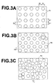
- Figs. 3A to 3C are diagrammatic plan views of preferable examples of a base on which a GaN layer having a plurality of holes are to be formed. That is, Figs. 3A to 3C schematically show preferable examples of arrangement of growth suppression mask elements.
- the dot-like mask elements are arranged four-fold symmetrically so that the width Ax of each dot-like mask element and the interval Bx between adjacent dot-like mask elements in the lateral direction are respectively identical to the width Ay of each dot-like mask element and the interval By between adjacent dot-like mask elements in the longitudinal direction.
- Fig. 3A the dot-like mask elements are arranged four-fold symmetrically so that the width Ax of each dot-like mask element and the interval Bx between adjacent dot-like mask elements in the lateral direction are respectively identical to the width Ay of each dot-like mask element and the interval By between adjacent dot-like mask elements in the longitudinal direction.
- the dot-like mask elements are arranged six-fold symmetrically so that every three adjacent dot-like mask elements form an equilateral triangle.
- the dot-like mask elements are randomly arranged.
- the minimum interval between each dot-like mask element and a nearest dot-like mask element e.g., the intervals Za, Zb, and Zc respectively indicated in Figs. 3A, 3B, and 3C
- the minimum interval between each dot-like mask element and a nearest dot-like mask element is 2.5 micrometers or smaller.
- the substrate as the second variation of the second embodiment is produced as follows.
- an n-type or p-type conductive GaN layer 9' which is doped with a conductive impurity and has a thickness of about 100 to 200 micrometers is formed on the GaN layer 9 in the construction of Fig. 2C.
- the substrate as the second variation of the second embodiment is obtained by removing from the structure of Fig. 5A the layers from the base substrate 1 to the GaN layer 9, as illustrated in Fig. 5B.
- materials used in the growth of the layers are trimethyl gallium (TMG), trimethyl aluminum (TMA), trimethyl indium (TMI), and ammonia.
- TMG trimethyl gallium
- TMA trimethyl aluminum
- TMI trimethyl indium
- ammonia silane gas is used as n-type dopant gas
- Cp 2 Mg cycropentadienyl magnesium
- the concrete example I is a concrete example of the substrate as the first embodiment of the present invention illustrated in Figs. 1A to 1D.
- the substrate as the concrete example I is produced as follows.
- a SiO 2 film 4 having a thickness of about 0.5 micrometers is formed on a (0001) face of a base substrate 1 made of sapphire, by plasma CVD (chemical vapor deposition) using SiH 4 gas and N 2 O gas.
- plasma CVD chemical vapor deposition
- a resist pattern (not shown) of a plurality of dot-like areas having a diameter of 2.5 micrometers or smaller and being arranged with a pitch equivalent to the dot diameter is formed on the SiO 2 film 4 by photolithography, and then the SiO 2 film 4 is etched by RIE (reactive ion etching) dry etching using the resist pattern and CHF 3 /O 2 gas. Thereafter, the resist pattern is removed by O 2 plasma ashing.
- a growth suppression mask 4a made of SiO 2 and patterned to have a plurality of discretely arranged dot-like areas is formed as illustrated in Fig. 1B. At this time, the growth suppression mask 4a occupies 40 to 90% of the entire area of the upper surface of the base substrate 1.
- a GaN buffer layer having a thickness of 20 nanometers (not shown) is grown at 500°C, and a first GaN layer 5 having a thickness of about 3 micrometers is grown at 1,050°C from exposed portions of the sapphire base substrate 1 (i.e., the portions of the sapphire base substrate 1 which are not covered by the growth suppression mask 4a) over the GaN buffer layer. Since the first GaN layer 5 is not grown from the growth suppression mask 4a, it has the plurality of holes 5b as illustrated in Fig. 1C.
- the first GaN layer 5 is also grown to some extent in lateral directions from the exposed portions of the sapphire base substrate 1 so that it is also formed over the edge portions of each of the plurality of dot-like (disk-like) mask elements constituting the growth suppression mask 4a. Therefore, the diameters of the plurality of holes 5b are slightly smaller than the diameters of the plurality of dot-like (disk-like) mask elements. At this time, it is preferable that the thickness of the first GaN layer 5 is equal to or greater than the diameters of the plurality of holes 5b.
- the growth suppression mask 4a made of SiO 2 is etched off with buffered hydrofluoric acid, and then a second GaN layer 6 is grown by MOCVD (metal organic chemical vapor deposition) at 1,080°C.
- MOCVD metal organic chemical vapor deposition
- the crystal growth of GaN is continued until regions above the plurality of holes 5b are closed by growth of GaN in lateral directions, and the upper surface of the second GaN layer 6 becomes even, as illustrated in Fig. 1D.
- the second GaN layer 6 having a low defect density is obtained.
- the present inventor has measured the etch pit density of the substrate formed as above. In the measurement, the etch pit density is counted after the substrate is dipped in an etching solution.
- the measured etch pit density of the substrate as the concrete example I is two to four orders of magnitude smaller than the etch pit densities of the substrates produced by the conventional production process.
- the concrete example II is a concrete example of the substrate as the second embodiment of the present invention illustrated in Figs. 2A to 2C.
- the base substrate 1 includes a main portion and a GaN layer formed on the main portion.
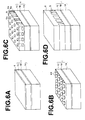
- FIGS. 6A to 6D are diagrammatic perspective views of structures in representative stages of a process for producing a substrate as the concrete example II.
- a GaN buffer layer 1B having a thickness of about 20 nm is formed on a (0001) face of a main portion 1A made of sapphire, by organometallic vapor phase epitaxy at 500°C, and then a GaN layer 1C having a thickness of about 2 micrometers is formed at 1,050°C.
- a base substrate 1 is obtained.
- SiO 2 film 4 having a thickness of about 0.5 micrometers is formed on the base substrate 1 by plasma CVD using SiH 4 gas and N 2 O gas.
- a resist pattern (not shown) of a plurality of dot-like areas having a diameter of 2.5 micrometers or smaller and being arranged with a pitch equivalent to the dot diameter is formed on the SiO 2 film 4 by photolithography, and then the SiO 2 film 4 is etched by RIE dry etching using the resist pattern and CHF 3 /O 2 gas. Thereafter, the resist pattern is removed by O 2 plasma ashing.
- a growth suppression mask 4a made of SiO 2 and patterned to have a plurality of discretely arranged dot-like areas is formed as illustrated in Fig. 6B. At this time, the growth suppression mask 4a occupies 40 to 90% of the entire area of the upper surface of the GaN layer 1C.
- a GaN layer 5 is grown at 1,050 °C from exposed portions of the GaN layer 1C (i.e., the portions of the GaN layer 1C which are not covered by the growth suppression mask 4a). Since GaN is not grown from the growth suppression mask 4a, the first GaN layer 5 has the plurality of holes 5b as illustrated in Fig. 6C. In addition, GaN is also grown to some extent in lateral directions from the exposed portions of the GaN layer 1C so that the first GaN layer 5 is also formed over the edge portions of each of the plurality of dot-like (disk-like) mask elements constituting the growth suppression mask 4a. Therefore, the diameters of the plurality of holes 5b are slightly smaller than the diameters of the plurality of dot-like (disk-like) mask elements.
- the growth suppression mask 4a made of SiO 2 is etched off with buffered hydrofluoric acid, and then a second GaN layer 6 is grown at 1,050°C.
- the crystal growth of GaN is continued until regions above the plurality of holes 5b are closed by growth of GaN in lateral directions and the upper surface of the second GaN layer 6 becomes even, as illustrated in Fig. 6D.
- the second GaN layer 6 having a low defect density is obtained.
- another growth suppression mask 7a is formed on the GaN layer 6 in a similar manner to the manner in which the growth suppression mask 4a is formed on the base substrate 1, as illustrated in Fig. 2A.
- a third GaN layer 8 having a plurality of holes 8b is formed over the GaN layer 6 by using the growth suppression mask 7a, as illustrated in Fig. 2B.
- a fourth GaN layer 9 is formed over the third GaN layer 8 as illustrated in Fig. 2C. It is possible to obtain a substrate having a reduced defect density by continuing the crystal growth until the upper surface of the GaN layer 9 becomes even.
- the present inventor has measured the etch pit density of the substrate formed as above.
- the measured etch pit density of the substrate as the concrete example II is two to six orders of magnitude smaller than the etch pit densities of the substrates produced by the conventional production process.
- the growth suppression masks 4a and 7a are removed in the concrete examples I and II, alternatively, the growth suppression masks 4a and 7a may not be removed, and the upper GaN layers 6 and 9 may be formed over the growth suppression masks 4a and 7a. That is, the growth suppression masks 4a and 7a may be embedded in the completed substrates.
- the concrete example III is another concrete example of the substrate as the second embodiment of the present invention illustrated in Figs. 2A to 2C.
- the growth suppression mask 7a is not removed.
- FIGS. 7A and 7B are diagrammatic perspective views of structures in representative stages of a process for producing a substrate as the concrete example III.
- a base substrate 1 is produced by forming by MOCVD a GaN buffer layer 1B and a GaN layer 1C on a main portion 1A made of SiC.
- a SiO 2 film 4 having a thickness of about 0.5 micrometers is formed on the GaN layer 1C of the base substrate 1 by plasma CVD using SiH 4 gas and N 2 O gas.
- a resist pattern (not shown) of a plurality of dot-like areas having a diameter of 2.5 micrometers or smaller and being arranged with a pitch equivalent to the dot diameter is formed on the SiO 2 film 4 by photolithography, and then the SiO 2 film 4 is etched by RIE (reactive ion etching) dry etching using the resist pattern and CHF 3 /O 2 gas. Thereafter, the resist pattern is removed by O 2 plasma ashing.
- a growth suppression mask 4a made of SiO 2 and patterned to have a plurality of discretely arranged dot-like areas is formed as illustrated in Fig. 6B. At this time, the growth suppression mask 4a occupies 40 to 90% of the entire area of the upper surface of the GaN layer 1C.
- a first GaN layer 5 having a thickness of about 3 micrometers is grown at 1,050 °C from exposed portions of the GaN layer 1C (i.e., the portions of the GaN layer 1C which are not covered by the growth suppression mask 4a). Since GaN is not grown from the growth suppression mask 4a, the first GaN layer 5 has the plurality of holes 5b as illustrated in Fig. 6C.
- a second GaN layer 6 is grown by MOCVD at 1,080°C. At this time, the crystal growth of GaN is continued until regions above the plurality of holes 5b are closed by growth of GaN in lateral directions, and the upper surface of the second GaN layer 6 becomes even, as illustrated in Fig. 7A. Thus, the second GaN layer 6 having a low defect density is obtained.
- another growth suppression mask 7a is formed on the second GaN layer 6 in a similar manner to the manner in which the growth suppression mask 4a is formed on the base substrate 1. Then, a third GaN layer 8 having a plurality of holes 8b is formed over the GaN layer 6 by using the growth suppression mask 7a. Subsequently, a fourth GaN layer 9 is formed over the third GaN layer 8. It is possible to obtain a substrate having a reduced defect density by continuing the crystal growth until the upper surface of the GaN layer 9 becomes even as illustrated in Fig. 7B.
- the present inventor has measured the etch pit density of the substrate formed as above.
- the measured etch pit density of the substrate as the concrete example III is four to six orders of magnitude smaller than the etch pit densities of the substrates produced by the conventional production process.
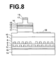
- the concrete example IV is a concrete example of a semiconductor laser element formed by using the substrate of the concrete example II.
- Fig. 8 is a diagrammatic cross-sectional view of the semiconductor laser element as the concrete example IV.
- an n-type GaN contact layer 10 an n-type Ga 1-z1 Al z1 N (2.5 nm)/GaN (2.5 nm) superlattice cladding layer 11, an n-type Ga 1-z2 Al z2 N optical waveguide layer 12, an In x2 Ga 1-x2 N (Si-doped)/Inx1Ga 1 -x1N multiple-quantum-well active layer 13 (0.5>x1>x2 ⁇ 0), a p-type Ga 1-z3 Al z3 N carrier blocking layer 14 (1 ⁇ zl>z3>z2 ⁇ 0), a p-type Ga 1-z2 Al z2 N optical waveguide layer 15, a p-type Ga 1-z1 Al z1 N (2.5 nm)/GaN (2.5 nm) superlattice cladding layer 16, and a p-type GaN contact layer 17 are formed on the GaN layer 9 in the substrate of the concrete example II.
- a first SiO 2 insulation film (not shown) and a first resist layer (not shown) are formed on the p-type GaN contact layer 17, and regions of the first resist layer and the first SiO 2 insulation film other than first stripe regions of the first resist layer and the first SiO 2 insulation film having a width of about 30 micrometers are removed by conventional lithography.
- the regions of the layered structures formed as above on both sides of the first stripe regions are etched to a mid-thickness of the p-type Ga 1- z1 Al z1 N (2.5 nm)/GaN (2.5 nm) superlattice cladding layer 16 by selective etching using RIE, where the thickness of the remaining superlattice cladding layer 16 is determined so as to realize an index-guided structure. Thereafter, the remaining regions of the first resist layer and the first SiO 2 insulation film are removed.
- a second SiO 2 insulation film (not shown) and a second resist layer (not shown) are formed over the layered structures formed as above, regions of the second resist layer and the second SiO 2 insulation film other than second stripe regions of the second resist layer and the second SiO 2 insulation film are removed, where the second stripe regions are located corresponding to the first stripe regions and 20 micrometers wider than the first stripe regions on each side of the first stripe regions. Then, the regions of the layered structures on both sides of the second stripe regions are etched by RIE until the n-type GaN contact layer 10 is exposed.
- an n electrode 18 made of Ti/Al is formed on the n-type GaN contact layer 10, and a p electrode 19 made of Ni/Au is formed on the remaining stripe region of the p-type GaN contact layer 17.
- the substrate is polished and cleaved so as to form resonator surfaces.
- a high reflectance coating and a low reflectance coating are applied to the resonator surfaces produced by the cleavage, and the layered structure thus formed is formed into a chip of a semiconductor laser element.
- the oscillation wavelength of the semiconductor laser element as the concrete example IV can be controlled in the range of 380 to 550 nm.
- the semiconductor laser element as the concrete example IV is an index-guided semiconductor laser element having a ridge structure and a large stripe width of 30 micrometers
- the substrates according to the present invention can also be used in other semiconductor elements including other semiconductor laser elements.
- Such semiconductor laser elements may include index-guided semiconductor laser elements having an internal index-guided structure and index-guided semiconductor laser elements having a buried ridge structure.
- the substrates according to the present invention can be further used for production of index-guided semiconductor laser elements which have a ridge structure and a stripe width of about 1 to 2 micrometers and oscillate in a fundamental transverse mode.
- the conductivity types of the semiconductor layers in the concrete examples I to IV may be inverted. That is, the n-type and the p-type may be exchanged.
Abstract
Description
- The present invention relates to a substrate which is used in a semiconductor element. The present invention also relates to a process for producing a substrate which is used in a semiconductor element. The present invention further relates to a semiconductor element which uses the above substrate.
- Japanese Journal of Applied Physics Vol. 37 (1998) Part 2, pp. L1020 discloses a short-wavelength semiconductor laser device which emits laser light in the 410 nm band. This semiconductor laser device is produced as follows. First, a GaN layer is formed on a sapphire substrate, a stripe pattern of a SiO2 film is formed on the GaN layer, and a GaN thick film is formed by selective lateral growth from nuclei of the growth generated in stripe areas of the GaN layer which are not covered by the stripe pattern of the SiO2 mask. Then, a GaN substrate is obtained by separating the GaN thick film from the sapphire substrate. Next, an n-type GaN buffer layer, an n-type InGaN crack prevention layer, an n-type AlGaN/GaN modulation doped superlattice cladding layer, an n-type GaN optical waveguide layer, an n-InGaN/InGaN multiple-quantum-well active layer, a p-type AlGaN carrier block layer, a p-type GaN optical waveguide layer, a p-type AlGaN/GaN modulation doped superlattice cladding layer, and a p-type GaN contact layer are formed on the above GaN substrate. However, the highest output power obtained in the fundamental transverse mode by the above semiconductor laser devices is about 30 mW, and the semiconductor laser device is reliable in the output power range up to 30 mW.
- Since the conventional ELOG (epitaxial lateral overgrowth) substrates as above are produced by selective lateral growth from nuclei of the growth generated in stripe areas of a GaN layer which are not covered by SiO2 mask, defects are reduced in the region produced by the selective lateral growth of GaN.
- Nevertheless, according to the conventional method as above, the density of the nuclei for growth is high, and therefore the spaces between the nuclei are bridged before the grown nuclei become large. Thus, defects are likely to be produced in the bridged regions. Although the GaN thick film is required to have a certain thickness in order to use the GaN thick film as a substrate, the defect density is increased with increase in the thickness. Even when the defect densities in the bridged regions are low, the defect density increases with the increase in the thickness, Consequently, it is difficult to form a wide low-defect region. That is, the conventional ELOG substrates have only a small low-defect region.
- In order to realize a reliable semiconductor laser device, an optical waveguide is required to be formed on a low-defect region of a substrate. Therefore, the conventional ELOG substrates are effective for producing semiconductor laser devices having a narrow stripe structure as disclosed in the aforementioned reference. However, it is impossible to form a reliable semiconductor laser device having a broad stripe structure on the conventional ELOG substrates.
- In order to realize a reliable semiconductor laser device having high output power, the semiconductor laser device is required to have a broad stripe structure, and in order to realize a reliable semiconductor laser device having a broad stripe structure, the semiconductor laser device is required to be formed on a GaN substrate which includes a wide low-defect region, instead of the conventional ELOG substrates.
- Generally, reliability of any semiconductor elements constituted by semiconductor layers formed on a substrate, including semiconductor laser devices, depends on defect densities in the substrate. Therefore, a substrate including a wide low-defect region is required for every type of semiconductor element.
- An object of the present invention is to provide a substrate which is used in a semiconductor element, and in which the defect density is low in a wide region.
- Another object of the present invention is to provide process for producing a substrate which is used in a semiconductor element, and in which the defect density is low in a wide region.
- A further object of the present invention is to provide a semiconductor element which uses a substrate in which the defect density is low in a wide region.
- (1) According to the first aspect of the present
invention, there is provided a process for producing a
substrate for use in a semiconductor element, comprising
the steps of: (a) forming on a surface of a base
substrate a first growth suppression mask constituted by
a plurality of first mask elements being discretely
arranged and each having a width of 2.5 micrometers or
smaller; (b) forming on the surface of the base
substrate a first GaN layer having a plurality of holes
by growing GaN from areas of the surface of the base
substrate which are not covered by the plurality of
first mask elements; and (c) forming a second GaN layer
over the first GaN layer.
Preferably, the process according to the first
aspect of the present invention may have one or any
possible combination of the following additional
features (i) to (iii).
- (i) The process according to the first aspect of the present invention may further comprise, between the steps (b) and (c), a step for removing the first growth suppression mask.
- (ii) The process according to the first aspect of the present invention may further comprise, after the step (c), the steps of: (d) forming on the second GaN layer a second growth suppression mask constituted by a plurality of second mask elements being discretely arranged and each having a width of 2.5 micrometers or smaller; (e) forming on the second GaN layer a third GaN layer having a plurality of holes by growing GaN from areas of the second GaN layer which are not covered by the plurality of second mask elements; and (f) forming a fourth GaN layer over the third GaN layer.
- (iii) The process according to the first aspect of the present invention having the feature (ii) may further comprise, between the steps (e) and (f), a step for removing the first growth suppression mask.
- (2) According to the second aspect of the present
invention, there is provided a process for producing a
substrate for use in a semiconductor element by
formation of a plurality of substrate layers on a
surface of a base substrate, where the formation is
realized by at least one predetermined sequence of
operations, and each of the at least one predetermined
sequence of operations includes the steps of: (a)
forming on a base surface a growth suppression mask
constituted by a plurality of mask elements being
discretely arranged and each having a width of 2.5
micrometers or smaller; (b) forming on the base surface
a first GaN layer having a plurality of holes by growing
GaN from areas of the base surface which are not covered
by the plurality of mask elements; and (c) forming a
second GaN layer over the first GaN layer.
That is, the above predetermined sequence of
operations including the steps (a) to (c) may be
performed once or a plurality of times. In each sequence
of operations, a group of layers including the growth
suppression mask, the first GaN layer, and the second
GaN layer are formed. When the predetermined sequence of
operations is performed a plurality of times, a
plurality of groups of layers each including the growth
suppression mask, the first GaN layer, and the second
GaN layer are stacked. In the above description of the
second aspect of the present invention, the base surface
referred to in step (a) is a surface of the base
substrate when the first group of layers are formed
directly on the surface of the base substrate, and the
base surface referred to in step (a) is a surface of the
second GaN layer in a precedingly formed group of layers
when a group of layers are formed on the precedingly
formed group of layers.Preferably, the process according to the second
aspect of the present invention may have one or any
possible combination of the following additional
features (i) to (viii).
- (i) The process according to the second aspect of the present invention may further comprise, between the steps (b) and (c), a step for removing the second growth suppression mask.
- (ii) The distance between each of the plurality of mask elements and one of the plurality of mask elements nearest to each of the plurality of mask elements is equal to or smaller than 2.5 micrometers.
- (iii) In the process according to the second aspect of the present invention, the plurality of mask elements cover 40 to 90% of the entire base surface.
- (iv) In the process according to the second aspect of the present invention, the growth suppression mask is made of a dielectric material. The dielectric material is, for example, SiO2, Al2O3, or SiN.
- (v) The process according to the second aspect of the present invention may further comprise a step for forming as an uppermost layer of the substrate a conductive GaN layer which is doped with a conductive impurity.
- (vi) In the process according to the second aspect of the present invention, the at least a portion of the base substrate including the surface is made of one of GaN, sapphire, SiC, ZnO, LiGaO2, LiAlO2, ZrB2, GaAs, GaP, Ge, and Si.
- (vii) The process according to the second aspect of the present invention may further comprise a step for removing the base substrate.
- (viii) The process according to the second aspect of the present invention may further comprise a step of separating an uppermost one of the plurality of layers from the other of the plurality of layers.
- (3) According to the third aspect of the present invention, there is provided a substrate for use in a semiconductor element, comprising: a base substrate; a first GaN layer having a plurality of holes which are discretely arranged and being formed on a surface of the base substrate by growing GaN from areas of the surface of the base substrate which are not covered by a plurality of first mask elements constituting a first growth suppression mask, being discretely arranged, and each having a width of 2.5 micrometers or smaller; and a second GaN layer formed over the first GaN layer. The substrate according to the third aspect of the present invention may further comprise: a third GaN layer having a plurality of holes which are discretely arranged and being formed on a surface of the second GaN layer by growing GaN from areas of the surface of the second GaN layer which are not covered by a plurality of second mask elements constituting a second growth suppression mask, being discretely arranged, and each having a width of 2.5 micrometers or smaller; and a fourth GaN layer formed over the third GaN layer.
- (4) According to the fourth aspect of the present
invention, there is provided a substrate for use in a
semiconductor element, comprising a base substrate and a
plurality of substrate layers formed on the base
substrate, and the plurality of substrate layers include
at least one group of layers. Each of the at least one
group of layers includes: a first GaN layer having a
plurality of holes which are discretely arranged and
being formed on a base surface by growing GaN from areas
of the base surface which are not covered by a plurality
of mask elements constituting a growth suppression mask,
being discretely arranged, and each having a width of
2.5 micrometers or smaller; and a second GaN layer
formed over the first GaN layer.
Preferably, the substrate according to the fourth
aspect of the present invention may have one or any
possible combination of the following additional
features (i) to (v).
- (i) The distance between each of the plurality of mask elements and one of the plurality of mask elements nearest to each of the plurality of mask elements is equal to or smaller than 2.5 micrometers.
- (ii) The plurality of mask elements cover 40 to 90% of the entire base surface.
- (iii) The growth suppression mask is made of a dielectric material.
- (iv) The substrate according to the fourth aspect of the present invention further comprise a conductive GaN layer which is doped with a conductive impurity and formed as an uppermost layer of the substrate.
- (v) In the substrate according to the fourth aspect of the present invention, at least a portion of the base substrate including the surface of the base substrate is made of one of GaN, sapphire, SiC, ZnO, LiGaO2, LiAlO2, ZrB2, GaAs, GaP, Ge, and Si.
- (5) According to the fifth aspect of the present invention, there is provided a semiconductor element for use in a semiconductor element, comprising at least one group of substrate layers, where each of the at least one group of substrate layers includes: a first GaN layer having a plurality of holes which are discretely arranged and being formed on a base surface by growing GaN from areas of the base surface which are not covered by a plurality of mask elements constituting a growth suppression mask, being discretely arranged, and each having a width of 2.5 micrometers or smaller; and a second GaN layer formed over the first GaN layer.
- (6) According to the sixth aspect of the present
invention, there is provided a substrate for use in a
semiconductor element, comprising a base substrate and a
plurality of substrate layers formed on the base
substrate. The plurality of substrate layers include at
least one group of layers, and each of the at least one
group of layers includes: a first GaN layer being formed
on a base surface and having a plurality of holes which
are discretely arranged and each of which has a width of
2.5 micrometers or smaller; and a second GaN layer
formed over the first GaN layer.
Preferably, the substrate according to the sixth
aspect of the present invention may have one or any
possible combination of the following additional
features (i) to (vi).
- (i) The substrate according to the sixth aspect of the present invention may further comprise a growth suppression mask constituted by a plurality of mask elements being discretely arranged on the base surface and each having a width of 2.5 micrometers or smaller.
- (ii) In the substrate according to the sixth aspect of the present invention having the feature (i), the distance between each of the plurality of mask elements and one of the plurality of mask elements nearest to each of the plurality of mask elements is equal to or smaller than 2.5 micrometers.
- (iii) In the substrate according to the sixth aspect of the present invention having the feature (i), the plurality of mask elements cover 40 to 90% of the entire base surface.
- (iv) In the substrate according to the sixth aspect of the present invention having the feature (i), the growth suppression mask is made of a dielectric material.
- (v) The substrate according to the sixth aspect of the present invention may further comprise a conductive GaN layer which is doped with a conductive impurity and formed as an uppermost layer of the substrate.
- (vi) In the substrate according to the sixth aspect of the present invention, at least a portion of the base substrate including the surface of the base substrate is made of one of GaN, sapphire, SiC, ZnO, LiGaO2, LiAlO2, ZrB2, GaAs, GaP, Ge, and Si. For example, the entire base substrate may be made of one of GaN, sapphire, SiC, ZnO, LiGaO2, LiAlO2, ZrB2, GaAs, GaP, Ge, and Si. Alternatively, the base substrate may be constituted by a main portion and a GaN layer formed on the main portion, where the main portion is made of one of GaN, sapphire, SiC, ZnO, LiGaO2, LiAlO2, ZrB2, GaAs, GaP, Ge, and Si.
- (7) According to the seventh aspect of the present invention, there is provided a semiconductor element for use in a semiconductor element, comprising at least one group of substrate layers, where each of the at least one group of substrate layers includes: a first GaN layer being formed on a base surface and having a plurality of holes which are discretely arranged and each of which has a width of 2.5 micrometers or smaller; and a second GaN layer formed over the first GaN layer.
- (8) According to the eighth aspect of the present invention, there is provided a substrate for use in a semiconductor element, which is produced through the steps of: (a) forming a plurality of substrate layers on a surface of a base substrate by performing at least one predetermined sequence of operations; and (b) separating an uppermost one of the plurality of substrate layers from the other of the plurality of substrate layers. Each of the at least one predetermined sequence of operations includes the substeps of: (a1) forming on a base surface a growth suppression mask constituted by a plurality of mask elements being discretely arranged and each having a width of 2.5 micrometers or smaller; (a2) forming on the base surface a first GaN layer having a plurality of holes by growing GaN from areas of the base surface which are not covered by the plurality of mask elements; and (a3) forming a second GaN layer over the first GaN layer. In this case, the uppermost one of the plurality of substrate layers may be a conductive GaN layer which is doped with a conductive impurity.
- (9) According to the ninth aspect of the present invention, there is provided a semiconductor element comprising a substrate and semiconductor layers formed on the substrate. The substrate is one of the substrates according to the third to eighth aspects of the present invention, where the substrates according to the third to eighth aspects of the present invention may have one or any combination of the aforementioned additional features.
- (10) The advantages of the present invention are as follows.
-
- In the processes according to the first and second aspects of the present invention, a (first) growth suppression mask which is constituted by a plurality of (first) mask elements being discretely arranged and each having a width of 2.5 micrometers or smaller is formed on a surface of a base substrate; a first GaN layer having a plurality of holes is formed on the surface of the base substrate by growing GaN from areas of the surface of the base substrate which are not covered by the plurality of first mask elements; and a second GaN layer is formed over the first GaN layer by crystal growth. Therefore, the density of the nuclei of growth can be reduced compared with the conventional process. Thus, it is possible to obtain a GaN layer having a wide low-defect region, and the obtained GaN layer can be used as a reliable substrate.
- When the sequence of operations of forming a growth suppression mask, a first GaN layer having a plurality of holes, and a second GaN layer is repeated two or more times in the second aspect of the present invention, it is possible to obtain a GaN layer having further lower defect density.
- In addition, since the first GaN layer having a plurality of holes is formed by forming on a base surface a growth suppression mask constituted by a plurality of mask elements being discretely arranged and each having a width of 2.5 micrometers or smaller, and growing GaN from areas of the base surface which are not covered by the plurality of mask elements, the formation of the first GaN layer having the plurality of holes according to the present invention is easier than other formation processes, for example, a process in which a GaN layer having a plurality of holes is formed by first forming a GaN layer which has no holes, and then producing holes by etching or the like.
- When the plurality of mask elements cover 40 to 90% of the entire base surface, the diameters of the plurality of holes formed in the first GaN layer are equivalent to the diameters of the plurality of mask elements constituting the growth suppression mask, and the plurality of holes formed in the first GaN layer occupy approximately 40 to 90% of the entire area of the first GaN layer. Therefore, when the second GaN layer is formed over the first GaN layer as above, the nuclei of growth can be effectively reduced. Thus, it is possible to obtain a GaN layer having low defect density.
- In addition, when a conductive GaN layer is formed as an uppermost layer of the substrate, it is possible to obtain a conductive GaN layer having low defect density.
- Further, since the semiconductor element according to the ninth aspect of the present invention is realized by forming semiconductor layers on one of the substrates according to the present invention, reliability of the semiconductor elements is high.
-
- Figs. 1A to 1D are diagrammatic perspective views of structures in representative stages of a process for producing a substrate as a first embodiment of the present invention.
- Figs. 2A to 2C are diagrammatic perspective views of structures in representative stages of a process for producing a substrate as a second embodiment of the present invention.
- Figs. 3A to 3C are diagrams schematically illustrating examples of arrangement of growth suppression mask elements.
- Fig. 4 is a diagrammatic perspective view of a first variation of the substrate as the second embodiment of the present invention, where the base substrate is removed from the substrate as the second embodiment.
- Figs. 5A and 5B are diagrammatic perspective views of structures in representative stages of a process for producing a second variation of the substrate as the second embodiment of the present invention.
- Figs. 6A to 6D are diagrammatic perspective views of structures in representative stages of a process for producing a substrate as the concrete example II.
- Figs. 7A and 7B are diagrammatic perspective views of structures in representative stages of a process for producing a substrate as the concrete example III.
- Fig. 8 is a diagrammatic cross-sectional view of the concrete example IV, which is a semiconductor laser element formed by using the substrate as the concrete example II or III.
-
- Embodiments of the present invention are explained in detail below with reference to the drawings.
- Figs. 1A to 1D are diagrammatic perspective views of structures in representative stages of a process for producing a substrate for use in a semiconductor element in the first embodiment of the present invention, where Fig. 1D shows the completed structure of the substrate as the first embodiment.
- As illustrated in Fig. 1D, the substrate for use in a semiconductor element, as the first embodiment of the present invention, comprises a
base substrate 1, afirst GaN layer 5 formed on thebase substrate 1, and asecond GaN layer 6 formed over thefirst GaN layer 5 by crystal growth, where a plurality ofholes 5b are formed in thefirst GaN layer 5. - The substrate as the first embodiment is produced as follows.
- First, a SiO2 film 4 is formed on the
base substrate 1 as illustrated in Fig. 1A, and then agrowth suppression mask 4a constituted by a plurality of dot-like (disk-like) mask elements made of SiO2 are formed on thebase substrate 1, where the plurality of dot-like (disk-like) mask elements are discretely arranged on the upper surface of thebase substrate 1 as illustrated in Fig. 1B. Subsequently, thefirst GaN layer 5 having the plurality ofholes 5b is formed over thebase substrate 1 as illustrated in Fig. 1C by growing a GaN layer from the portions of the upper surface of thebase substrate 1 which are not covered by thegrowth suppression mask 4a. Thereafter, thegrowth suppression mask 4a is removed, and thesecond GaN layer 6 is grown over thefirst GaN layer 5 until the upper surface of thesecond GaN layer 6 becomes even, as illustrated in Fig. 1D. - It is preferable that the maximum width (the maximum diameter) of each of the plurality of dot-like (disk-like) mask elements constituting the
growth suppression mask 4a is 2.5 micrometers or smaller, and thegrowth suppression mask 4a covers 40 to 90% of the upper surface of thebase substrate 1. In addition, theGaN layer 5 is formed so that the plurality ofholes 5b formed in thefirst GaN layer 5 have the same diameters as the plurality of dot-like (disk-like) mask elements, and therefore 40 to 90% of the upper surface of thebase substrate 1 is not covered by thefirst GaN layer 5. Further, it is preferable that the thickness of thefirst GaN layer 5 is equal to or greater than the diameters of the plurality of dot-like (disk-like) mask. - When the above
growth suppression mask 4a is used, it is easy to form thefirst GaN layer 5 having the plurality ofholes 5b. When thesecond GaN layer 6 is formed over thefirst GaN layer 5 by selective lateral growth, the density of the nuclei of growth can be reduced compared with the conventional ELOG substrates. In addition, defects caused by strains due to lattice mismatching with the substrate can be reduced. - Further, it is considered that when the
second GaN layer 6 is grown over thefirst GaN layer 5 by selective lateral growth, nuclei of growth are generated on the upper surface of thefirst GaN layer 5 and inner surfaces of the plurality ofholes 5b. When the diameters and depths of the plurality ofholes 5b are set so as to satisfy a predetermined relationship, e.g., when the maximum width of the plurality ofholes 5b is 1 micrometer or smaller, and the depths of the plurality ofholes 5b are appropriately set corresponding to the maximum width of the plurality ofholes 5b, the top portions of the plurality ofholes 5b are closed with portions of thesecond GaN layer 6 laterally grown from nuclei of growth generated on the upper surface of thefirst GaN layer 5 before the plurality ofholes 5b are fully filled with thesecond GaN layer 6. That is, it is possible to produce spaces in lower portions of the plurality ofholes 5b. When such spaces exist, defects caused by strains due to a difference in the thermal expansion coefficient from the substrate can be reduced. - Figs. 2A to 2C are diagrammatic perspective views of structures in representative stages of a process for producing a substrate as the second embodiment of the present invention, where Fig. 2C shows the completed structure of the substrate as the second embodiment.
- As illustrated in Figs. 2A to 2C, the substrate as the second embodiment is produced by performing again the operations for producing the substrate as the first embodiment, on the substrate as the first embodiment. That is, the substrate as the second embodiment is produced as follows.
- First, another
growth suppression mask 7a is formed on thesecond GaN layer 6 in the substrate as the first embodiment in a similar manner to the manner in which thegrowth suppression mask 4a is formed on thebase substrate 1, as illustrated in Fig. 2A. Then, athird GaN layer 8 having a plurality ofholes 8b is formed on thesecond GaN layer 6 by using thegrowth suppression mask 7a, as illustrated in Fig. 2B. Subsequently, afourth GaN layer 9 is formed by selective lateral growth over thethird GaN layer 8 as illustrated in Fig. 2C. - When formation of a first GaN layer having a plurality of holes and formation of a second GaN layer over the first GaN layer having the plurality of holes are repeated, it is possible to obtain a GaN layer in which defects are further reduced. The formation of the first and second GaN layers may be repeated more than two times.
- The growth suppression mask may be made of any other material which can suppress growth of GaN. For example, growth suppression mask may be made of another dielectric material such as alumina (Al2O3) or silicon nitride (SiN), instead of SiO2.
- Figs. 3A to 3C are diagrammatic plan views of preferable examples of a base on which a GaN layer having a plurality of holes are to be formed. That is, Figs. 3A to 3C schematically show preferable examples of arrangement of growth suppression mask elements. In the example of Fig. 3A, the dot-like mask elements are arranged four-fold symmetrically so that the width Ax of each dot-like mask element and the interval Bx between adjacent dot-like mask elements in the lateral direction are respectively identical to the width Ay of each dot-like mask element and the interval By between adjacent dot-like mask elements in the longitudinal direction. In the example of Fig. 3B, the dot-like mask elements are arranged six-fold symmetrically so that every three adjacent dot-like mask elements form an equilateral triangle. In the example of Fig. 3C, the dot-like mask elements are randomly arranged. However, in any arrangement, it is preferable that the minimum interval between each dot-like mask element and a nearest dot-like mask element (e.g., the intervals Za, Zb, and Zc respectively indicated in Figs. 3A, 3B, and 3C) is 2.5 micrometers or smaller.
-
- (1) Although the dot-like mask elements have a circular form in the above example, the dot-like mask elements may have a polygonal form or an arbitrary form.
- (2) Preferably, at least a portion of the
base substrate 1 including the surface of thebase substrate 1, on which the growth suppression mask is formed, is made of one of GaN, sapphire, SiC, ZnO, LiGaO2, LiAlO2, ZrB2, GaAs, GaP, Ge, and Si. For example, theentire base substrate 1 may be made of one of GaN, sapphire, SiC, ZnO, LiGaO2, LiAlO2, ZrB2, GaAs, GaP, Ge, and Si. Alternatively, the base substrate may be constituted by a main portion made of one of GaN, sapphire, SiC, ZnO, LiGaO2, LiAlO2, ZrB2, GaAs, GaP, Ge, and Si, and a GaN layer formed on the main portion. - (3) Although the constructions of the first and
second embodiments each including the layers from the
base substrate 1 to the uppermost GaN layer as illustrated in Figs. 1D and 2C may be used as a substrate, it is possible to remove thebase substrate 1 from each of the constructions. For example, Fig. 4 shows a first variation of the substrate as the second embodiment. In the substrate of Fig. 4, thebase substrate 1 is removed from the substrate as the second embodiment. - (4) Although the GaN layers are undoped in the
first and second embodiments, n-type or p-type
conductive GaN layers, instead of the undoped GaN layers,
may be formed by doping the GaN layers with a conductive
impurity. In this case, a conductive substrate for use
in a semiconductor element can be obtained by removing
the
base substrate 1 after formation of the conductive GaN layers, for example, as illustrated in Fig. 4. - (5) Figs. 5A and 5B are diagrammatic perspective views of structures in representative stages of a process for producing a second variation of the substrate as the second embodiment of the present invention, where Fig. 5B shows the second variation of the substrate as the second embodiment.
-
- The substrate as the second variation of the second embodiment is produced as follows.
- First, as illustrated in Fig. 5A, an n-type or p-type conductive GaN layer 9' which is doped with a conductive impurity and has a thickness of about 100 to 200 micrometers is formed on the
GaN layer 9 in the construction of Fig. 2C. Then, the substrate as the second variation of the second embodiment is obtained by removing from the structure of Fig. 5A the layers from thebase substrate 1 to theGaN layer 9, as illustrated in Fig. 5B. -
- (1) In the substrates as the first and second embodiments and their variations, defect densities in the uppermost GaN layers are reduced. Therefore, when semiconductor elements are produced by forming semiconductor layers on these substrates, reliability of the semiconductor elements can be increased.
- (2) When semiconductor elements such as semiconductor laser elements are produced by forming semiconductor layers (for example, including an active layer) on a conductive substrate, an electrode can be formed on the back surface of the substrate. Therefore, processes for producing the semiconductor elements can be simplified.
- (3) Since the defect densities in the substrates according to the present invention are low, the substrates according to the present invention are reliable, and can be used in production of semiconductor elements and optical or electronic devices in the fields of high-speed, information processing, image processing, communications, laser measurement, medicine, printing, and the like, where the semiconductor elements and the optical or electronic devices include field effect transistors, semiconductor laser devices, semiconductor optical amplifiers, light emitting devices, optical detectors, and the like.
-
- Concrete examples of processes for producing the substrates as the embodiments of the present invention are explained below.
- In the following concrete examples I to IV, materials used in the growth of the layers are trimethyl gallium (TMG), trimethyl aluminum (TMA), trimethyl indium (TMI), and ammonia. In addition, silane gas is used as n-type dopant gas, and cycropentadienyl magnesium (Cp2Mg) is used as p-type dopant gas.
- The concrete example I is a concrete example of the substrate as the first embodiment of the present invention illustrated in Figs. 1A to 1D.
- The substrate as the concrete example I is produced as follows.
- First, as illustrated in Fig. 1A, a SiO2 film 4 having a thickness of about 0.5 micrometers is formed on a (0001) face of a
base substrate 1 made of sapphire, by plasma CVD (chemical vapor deposition) using SiH4 gas and N2O gas. - Subsequently, a resist pattern (not shown) of a plurality of dot-like areas having a diameter of 2.5 micrometers or smaller and being arranged with a pitch equivalent to the dot diameter is formed on the SiO2 film 4 by photolithography, and then the SiO2 film 4 is etched by RIE (reactive ion etching) dry etching using the resist pattern and CHF3/O2 gas. Thereafter, the resist pattern is removed by O2 plasma ashing. Thus, a
growth suppression mask 4a made of SiO2 and patterned to have a plurality of discretely arranged dot-like areas is formed as illustrated in Fig. 1B. At this time, thegrowth suppression mask 4a occupies 40 to 90% of the entire area of the upper surface of thebase substrate 1. - Next, a GaN buffer layer having a thickness of 20 nanometers (not shown) is grown at 500°C, and a
first GaN layer 5 having a thickness of about 3 micrometers is grown at 1,050°C from exposed portions of the sapphire base substrate 1 (i.e., the portions of thesapphire base substrate 1 which are not covered by thegrowth suppression mask 4a) over the GaN buffer layer. Since thefirst GaN layer 5 is not grown from thegrowth suppression mask 4a, it has the plurality ofholes 5b as illustrated in Fig. 1C. In addition, thefirst GaN layer 5 is also grown to some extent in lateral directions from the exposed portions of thesapphire base substrate 1 so that it is also formed over the edge portions of each of the plurality of dot-like (disk-like) mask elements constituting thegrowth suppression mask 4a. Therefore, the diameters of the plurality ofholes 5b are slightly smaller than the diameters of the plurality of dot-like (disk-like) mask elements. At this time, it is preferable that the thickness of thefirst GaN layer 5 is equal to or greater than the diameters of the plurality ofholes 5b. - Thereafter, the
growth suppression mask 4a made of SiO2 is etched off with buffered hydrofluoric acid, and then asecond GaN layer 6 is grown by MOCVD (metal organic chemical vapor deposition) at 1,080°C. At this time, the crystal growth of GaN is continued until regions above the plurality ofholes 5b are closed by growth of GaN in lateral directions, and the upper surface of thesecond GaN layer 6 becomes even, as illustrated in Fig. 1D. Thus, thesecond GaN layer 6 having a low defect density is obtained. - The present inventor has measured the etch pit density of the substrate formed as above. In the measurement, the etch pit density is counted after the substrate is dipped in an etching solution. The measured etch pit density of the substrate as the concrete example I is two to four orders of magnitude smaller than the etch pit densities of the substrates produced by the conventional production process.
- The concrete example II is a concrete example of the substrate as the second embodiment of the present invention illustrated in Figs. 2A to 2C. In the concrete examples II to IV, the
base substrate 1 includes a main portion and a GaN layer formed on the main portion. - A process for producing the substrate as the concrete example II is explained below with reference to Figs. 6A to 6D, which are diagrammatic perspective views of structures in representative stages of a process for producing a substrate as the concrete example II.
- First, as illustrated in Fig. 6A, a
GaN buffer layer 1B having a thickness of about 20 nm is formed on a (0001) face of amain portion 1A made of sapphire, by organometallic vapor phase epitaxy at 500°C, and then aGaN layer 1C having a thickness of about 2 micrometers is formed at 1,050°C. Thus, abase substrate 1 is obtained. - Thereafter, a SiO2 film 4 having a thickness of about 0.5 micrometers is formed on the
base substrate 1 by plasma CVD using SiH4 gas and N2O gas. - Subsequently, a resist pattern (not shown) of a plurality of dot-like areas having a diameter of 2.5 micrometers or smaller and being arranged with a pitch equivalent to the dot diameter is formed on the SiO2 film 4 by photolithography, and then the SiO2 film 4 is etched by RIE dry etching using the resist pattern and CHF3/O2 gas. Thereafter, the resist pattern is removed by O2 plasma ashing. Thus, a
growth suppression mask 4a made of SiO2 and patterned to have a plurality of discretely arranged dot-like areas is formed as illustrated in Fig. 6B. At this time, thegrowth suppression mask 4a occupies 40 to 90% of the entire area of the upper surface of theGaN layer 1C. - Next, a
GaN layer 5 is grown at 1,050 °C from exposed portions of theGaN layer 1C (i.e., the portions of theGaN layer 1C which are not covered by thegrowth suppression mask 4a). Since GaN is not grown from thegrowth suppression mask 4a, thefirst GaN layer 5 has the plurality ofholes 5b as illustrated in Fig. 6C. In addition, GaN is also grown to some extent in lateral directions from the exposed portions of theGaN layer 1C so that thefirst GaN layer 5 is also formed over the edge portions of each of the plurality of dot-like (disk-like) mask elements constituting thegrowth suppression mask 4a. Therefore, the diameters of the plurality ofholes 5b are slightly smaller than the diameters of the plurality of dot-like (disk-like) mask elements. - Thereafter, the
growth suppression mask 4a made of SiO2 is etched off with buffered hydrofluoric acid, and then asecond GaN layer 6 is grown at 1,050°C. At this time, the crystal growth of GaN is continued until regions above the plurality ofholes 5b are closed by growth of GaN in lateral directions and the upper surface of thesecond GaN layer 6 becomes even, as illustrated in Fig. 6D. Thus, thesecond GaN layer 6 having a low defect density is obtained. - Further, by the same steps as shown in Figure 6b through Figure 6d, another
growth suppression mask 7a is formed on theGaN layer 6 in a similar manner to the manner in which thegrowth suppression mask 4a is formed on thebase substrate 1, as illustrated in Fig. 2A. Then, athird GaN layer 8 having a plurality ofholes 8b is formed over theGaN layer 6 by using thegrowth suppression mask 7a, as illustrated in Fig. 2B. Subsequently, afourth GaN layer 9 is formed over thethird GaN layer 8 as illustrated in Fig. 2C. It is possible to obtain a substrate having a reduced defect density by continuing the crystal growth until the upper surface of theGaN layer 9 becomes even. - The present inventor has measured the etch pit density of the substrate formed as above. The measured etch pit density of the substrate as the concrete example II is two to six orders of magnitude smaller than the etch pit densities of the substrates produced by the conventional production process.
- Although the
growth suppression masks growth suppression masks growth suppression masks growth suppression masks - The concrete example III is another concrete example of the substrate as the second embodiment of the present invention illustrated in Figs. 2A to 2C. In the concrete example III, the
growth suppression mask 7a is not removed. - A process for producing the substrate as the concrete example III is explained below with reference to Figs. 7A and 7B, which are diagrammatic perspective views of structures in representative stages of a process for producing a substrate as the concrete example III.
- First, as illustrated in Fig. 6A, a
base substrate 1 is produced by forming by MOCVD aGaN buffer layer 1B and aGaN layer 1C on amain portion 1A made of SiC. - Then, a SiO2 film 4 having a thickness of about 0.5 micrometers is formed on the
GaN layer 1C of thebase substrate 1 by plasma CVD using SiH4 gas and N2O gas. - Subsequently, a resist pattern (not shown) of a plurality of dot-like areas having a diameter of 2.5 micrometers or smaller and being arranged with a pitch equivalent to the dot diameter is formed on the SiO2 film 4 by photolithography, and then the SiO2 film 4 is etched by RIE (reactive ion etching) dry etching using the resist pattern and CHF3/O2 gas. Thereafter, the resist pattern is removed by O2 plasma ashing. Thus, a
growth suppression mask 4a made of SiO2 and patterned to have a plurality of discretely arranged dot-like areas is formed as illustrated in Fig. 6B. At this time, thegrowth suppression mask 4a occupies 40 to 90% of the entire area of the upper surface of theGaN layer 1C. - Next, a
first GaN layer 5 having a thickness of about 3 micrometers is grown at 1,050 °C from exposed portions of theGaN layer 1C (i.e., the portions of theGaN layer 1C which are not covered by thegrowth suppression mask 4a). Since GaN is not grown from thegrowth suppression mask 4a, thefirst GaN layer 5 has the plurality ofholes 5b as illustrated in Fig. 6C. - Thereafter, a
second GaN layer 6 is grown by MOCVD at 1,080°C. At this time, the crystal growth of GaN is continued until regions above the plurality ofholes 5b are closed by growth of GaN in lateral directions, and the upper surface of thesecond GaN layer 6 becomes even, as illustrated in Fig. 7A. Thus, thesecond GaN layer 6 having a low defect density is obtained. - Further, another
growth suppression mask 7a is formed on thesecond GaN layer 6 in a similar manner to the manner in which thegrowth suppression mask 4a is formed on thebase substrate 1. Then, athird GaN layer 8 having a plurality ofholes 8b is formed over theGaN layer 6 by using thegrowth suppression mask 7a. Subsequently, afourth GaN layer 9 is formed over thethird GaN layer 8. It is possible to obtain a substrate having a reduced defect density by continuing the crystal growth until the upper surface of theGaN layer 9 becomes even as illustrated in Fig. 7B. - The present inventor has measured the etch pit density of the substrate formed as above. The measured etch pit density of the substrate as the concrete example III is four to six orders of magnitude smaller than the etch pit densities of the substrates produced by the conventional production process.
- The concrete example IV is a concrete example of a semiconductor laser element formed by using the substrate of the concrete example II. Fig. 8 is a diagrammatic cross-sectional view of the semiconductor laser element as the concrete example IV.
- As illustrated in Fig. 8, an n-type
GaN contact layer 10, an n-type Ga1-z1Alz1N (2.5 nm)/GaN (2.5 nm)superlattice cladding layer 11, an n-type Ga1-z2Alz2Noptical waveguide layer 12, an Inx2Ga1-x2N (Si-doped)/Inx1Ga1-x1N multiple-quantum-well active layer 13 (0.5>x1>x2 ≥ 0), a p-type Ga1-z3Alz3N carrier blocking layer 14 (1 ≥ zl>z3>z2 ≥ 0), a p-type Ga1-z2Alz2Noptical waveguide layer 15, a p-type Ga1-z1Alz1N (2.5 nm)/GaN (2.5 nm)superlattice cladding layer 16, and a p-type GaN contact layer 17 are formed on theGaN layer 9 in the substrate of the concrete example II. - Subsequently, a first SiO2 insulation film (not shown) and a first resist layer (not shown) are formed on the p-type GaN contact layer 17, and regions of the first resist layer and the first SiO2 insulation film other than first stripe regions of the first resist layer and the first SiO2 insulation film having a width of about 30 micrometers are removed by conventional lithography. Then, the regions of the layered structures formed as above on both sides of the first stripe regions are etched to a mid-thickness of the p-type Ga1- z1Alz1N (2.5 nm)/GaN (2.5 nm)
superlattice cladding layer 16 by selective etching using RIE, where the thickness of the remainingsuperlattice cladding layer 16 is determined so as to realize an index-guided structure. Thereafter, the remaining regions of the first resist layer and the first SiO2 insulation film are removed. - Next, a second SiO2 insulation film (not shown) and a second resist layer (not shown) are formed over the layered structures formed as above, regions of the second resist layer and the second SiO2 insulation film other than second stripe regions of the second resist layer and the second SiO2 insulation film are removed, where the second stripe regions are located corresponding to the first stripe regions and 20 micrometers wider than the first stripe regions on each side of the first stripe regions. Then, the regions of the layered structures on both sides of the second stripe regions are etched by RIE until the n-type
GaN contact layer 10 is exposed. - Thereafter, by using conventional lithography, an
n electrode 18 made of Ti/Al is formed on the n-typeGaN contact layer 10, anda p electrode 19 made of Ni/Au is formed on the remaining stripe region of the p-type GaN contact layer 17. Subsequently, the substrate is polished and cleaved so as to form resonator surfaces. Then, a high reflectance coating and a low reflectance coating are applied to the resonator surfaces produced by the cleavage, and the layered structure thus formed is formed into a chip of a semiconductor laser element. - Since, in the above semiconductor laser element, a wide stripe structure is formed on the low-
defect GaN layer 9, the reliability of the semiconductor laser element is high even in high output power operations. - When the composition of the active layer is appropriately controlled, the oscillation wavelength of the semiconductor laser element as the concrete example IV can be controlled in the range of 380 to 550 nm.
- Although the semiconductor laser element as the concrete example IV is an index-guided semiconductor laser element having a ridge structure and a large stripe width of 30 micrometers, the substrates according to the present invention can also be used in other semiconductor elements including other semiconductor laser elements. Such semiconductor laser elements may include index-guided semiconductor laser elements having an internal index-guided structure and index-guided semiconductor laser elements having a buried ridge structure. In addition, the substrates according to the present invention can be further used for production of index-guided semiconductor laser elements which have a ridge structure and a stripe width of about 1 to 2 micrometers and oscillate in a fundamental transverse mode.
- The conductivity types of the semiconductor layers in the concrete examples I to IV may be inverted. That is, the n-type and the p-type may be exchanged.
Claims (40)
- A process for producing a substrate for use in a semiconductor element, comprising the steps of:(a) forming on a surface of a base substrate a first growth suppression mask constituted by a plurality of first mask elements being discretely arranged and each having a width of 2.5 micrometers or smaller;(b) forming on said surface of the base substrate a first GaN layer having a plurality of holes by growing GaN from areas of the surface of the base substrate which are not covered by said plurality of first mask elements; and(c) forming a second GaN layer over said first GaN layer.
- A process according to claim 1, further comprising, between said steps (b) and (c), a step for removing said first growth suppression mask.
- A process according to claim 1, further comprising, after said step (c), the steps of,(d) forming on said second GaN layer a second growth suppression mask constituted by a plurality of second mask elements being discretely arranged and each having a width of 2.5 micrometers or smaller,(e) forming on said second GaN layer a third GaN layer having a plurality of holes by growing GaN from areas of the second GaN layer which are not covered by said plurality of second mask elements, and(f) forming a fourth GaN layer over said third GaN layer.
- A process according to claim 3, further comprising, between said steps (e) and (f), a step for removing said second growth suppression mask.
- A process for producing a substrate for use in a semiconductor element by formation of a plurality of substrate layers on a surface of a base substrate, where said formation is realized by at least one predetermined sequence of operations, and each of said at least one predetermined sequence of operations includes the steps of:(a) forming on a base surface a growth suppression mask constituted by a plurality of mask elements being discretely arranged and each having a width of 2.5 micrometers or smaller;(b) forming on said base surface a first GaN layer having a plurality of holes by growing GaN from areas of the base surface which are not covered by said plurality of mask elements; and(c) forming a second GaN layer over said first GaN layer.
- A process according to claim 5, further comprising, between said steps (b) and (c), a step for removing said growth suppression mask.
- A process according to claim 5, wherein a distance between each of said plurality of mask elements and one of the plurality of mask elements nearest to said each of said plurality of mask elements is equal to or smaller than 2.5 micrometers.
- A process according to claim 5, wherein said plurality of mask elements cover 40 to 90% of the entire base surface.
- A process according to claim 5, wherein said growth suppression mask is made of a dielectric material.
- A process according to claim 5, further comprising a step for forming as an uppermost layer of said substrate a conductive GaN layer which is doped with a conductive impurity.
- A process according to claim 5, wherein at least a portion of the base substrate including said surface of the base substrate is made of one of GaN, sapphire, SiC, ZnO, LiGaO2, LiAlO2, ZrB2, GaAs, GaP, Ge, and Si.
- A process according to claim 5, further comprising a step for removing said base substrate.
- A process according to claim 5, further comprising a step of separating an uppermost one of said plurality of substrate layers from other ones of said plurality of substrate layers.
- A semiconductor element comprising:wherein said substrate includes a base substrate and a plurality of substrate layers formed on said base substrate,a substrate; andsemiconductor layers formed on the substrate;
said plurality of substrate layers include at least one group of layers, and
each of the at least one group of layers includes,
a first GaN layer being formed on a base surface and having a plurality of holes which are discretely arranged and each of which has a width of 2.5 micrometers or smaller, and
a second GaN layer formed over said first GaN layer. - A semiconductor element according to claim 14, wherein each of the at least one group of layers further includes a growth suppression mask constituted by a plurality of mask elements being discretely arranged on said base surface and each having a width of 2.5 micrometers or smaller.
- A semiconductor element according to claim 15, wherein a distance between each of said plurality of mask elements and one of the plurality of mask elements nearest to said each of said plurality of mask elements is equal to or smaller than 2.5 micrometers.
- A semiconductor element according to claim 15, wherein said plurality of mask elements cover 40 to 90% of the entire base surface.
- A semiconductor element according to claim 15, wherein said growth suppression mask is made of a dielectric material.
- A semiconductor element according to claim 14, wherein said substrate further includes a conductive GaN layer which is doped with a conductive impurity and formed as an uppermost layer of said substrate.
- A semiconductor element according to claim 14, wherein at least a portion of the base substrate including said surface of the base substrate is made of one of GaN, sapphire, SiC, ZnO, LiGaO2, LiAlO2, ZrB2, GaAs, GaP, Ge, and Si.
- A semiconductor element comprising:wherein said substrate includes a plurality of substrate layers,a substrate; andsemiconductor layers formed on the substrate;
said plurality of substrate layers include at least one group of layers, and
each of the at least one group of layers includes,
a first GaN layer being having a plurality of holes which are discretely arranged and each of which has a width of 2.5 micrometers or smaller, and
a second GaN layer formed over said first GaN layer. - A semiconductor element, comprising:wherein said substrate is produced through the steps of:a substrate; andsemiconductor layers formed on the substrate;each of said at least one predetermined sequence of operations includes the substeps of,(a) forming a plurality of substrate layers on a surface of a base substrate by performing at least one predetermined sequence of operations; and(b) separating an uppermost one of said plurality of substrate layers from the other of said plurality of substrate layers; and(a1) forming on a base surface a growth suppression mask constituted by a plurality of mask elements being discretely arranged and each having a width of 2.5 micrometers or smaller,(a2) forming on said base surface a first GaN layer having a plurality of holes by growing GaN from areas of the base surface which are not covered by said plurality of mask elements, and(a3) forming a second GaN layer over said first GaN layer.
- A substrate for use in a semiconductor element, comprising:a base substrate;a first GaN layer having a plurality of holes which are discretely arranged and being formed on a surface of said base substrate by growing GaN from areas of the surface of the base substrate which are not covered by a plurality of first mask elements constituting a first growth suppression mask, being discretely arranged, and each having a width of 2.5 micrometers or smaller; anda second GaN layer formed over said first GaN layer.
- A substrate according to claim 23, further comprising,
a third GaN layer having a plurality of holes which are discretely arranged and being formed on a surface of said second GaN layer by growing GaN from areas of the surface of the second GaN layer which are not covered by a plurality of second mask elements constituting a second growth suppression mask, being discretely arranged, and each having a width of 2.5 micrometers or smaller, and
a fourth GaN layer formed over said third GaN layer. - A substrate for use in a semiconductor element, comprising:wherein said plurality of substrate layers include at least one group of layers, anda base substrate; anda plurality of substrate layers formed on said base substrate;
each of the at least one group of layers includes,
a first GaN layer having a plurality of holes which are discretely arranged and being formed on a base surface by growing GaN from areas of the base surface which are not covered by a plurality of mask elements constituting a growth suppression mask, being discretely arranged, and each having a width of 2.5 micrometers or smaller, and
a second GaN layer formed over said first GaN layer. - A substrate according to claim 25, wherein a distance between each of said plurality of mask elements and one of the plurality of mask elements nearest to said each of said plurality of mask elements is equal to or smaller than 2.5 micrometers.
- A substrate according to claim 25, wherein said plurality of mask elements cover 40 to 90% of the entire base surface.
- A substrate according to claim 25, wherein said growth suppression mask is made of a dielectric material.
- A substrate according to claim 25, further comprising a conductive GaN layer which is doped with a conductive impurity and formed as an uppermost layer of said substrate.
- A substrate according to claim 25, wherein at least a portion of the base substrate including said surface of the base substrate is made of one of GaN, sapphire, SiC, ZnO, LiGaO2, LiAlO2, ZrB2, GaAs, GaP, Ge, and Si.
- A semiconductor element for use in a semiconductor element, comprising at least one group of substrate layers, where each of the at least one group of substrate layers includes:a first GaN layer having a plurality of holes which are discretely arranged and being formed on a base surface by growing GaN from areas of the base surface which are not covered by a plurality of mask elements constituting a growth suppression mask, being discretely arranged, and each having a width of 2.5 micrometers or smaller; anda second GaN layer formed over said first GaN layer.
- A substrate for use in a semiconductor element, comprising:wherein said plurality of substrate layers include at least one group of layers, anda base substrate; anda plurality of substrate layers formed on said base substrate;
each of the at least one group of layers includes,
a first GaN layer being formed on a base surface and having a plurality of holes which are discretely arranged and each of which has a width of 2.5 micrometers or smaller, and
a second GaN layer formed over said first GaN layer. - A substrate according to claim 32, further comprising a growth suppression mask constituted by a plurality of mask elements being discretely arranged on said base surface and each having a width of 2.5 micrometers or smaller.
- A substrate according to claim 33, wherein a distance between each of said plurality of mask elements and one of the plurality of mask elements nearest to said each of said plurality of mask elements is equal to or smaller than 2.5 micrometers.
- A substrate according to claim 33, wherein said plurality of mask elements cover 40 to 90% of the entire base surface.
- A substrate according to claim 33, wherein said growth suppression mask is made of a dielectric material.
- A substrate according to claim 32, further comprising a conductive GaN layer which is doped with a conductive impurity and formed as an uppermost layer of said substrate.
- A substrate according to claim 32, wherein at least a portion of the base substrate including said surface of the base substrate is made of one of GaN, sapphire, SiC, ZnO, LiGaO2, LiAlO2, ZrB2, GaAs, GaP, Ge, and Si.
- A semiconductor element for use in a semiconductor element, comprising at least one group of substrate layers, where each of the at least one group of substrate layers includes:a first GaN layer being formed on a base surface and having a plurality of holes which are discretely arranged and each of which has a width of 2.5 micrometers or smaller; anda second GaN layer formed over said first GaN layer.
- A substrate for use in a semiconductor element, which is produced through the steps of:each of said at least one predetermined sequence of operations includes the substeps of,(a) forming a plurality of substrate layers on a surface of a base substrate by performing at least one predetermined sequence of operations; and(b) separating an uppermost one of said plurality of substrate layers from the other of said plurality of substrate layers; and
(a1) forming on a base surface a growth suppression mask constituted by a plurality of mask elements being discretely arranged and each having a width of 2.5 micrometers or smaller,
(a2) forming on said base surface a first GaN layer having a plurality of holes by growing GaN from areas of the base surface which are not covered by said plurality of mask elements, and
(a3) forming a second GaN layer over said first GaN layer.
Applications Claiming Priority (4)
| Application Number | Priority Date | Filing Date | Title |
|---|---|---|---|
| JP2001272895 | 2001-09-10 | ||
| JP2001272895 | 2001-09-10 | ||
| JP2002134089 | 2002-05-09 | ||
| JP2002134089 | 2002-05-09 |
Publications (2)
| Publication Number | Publication Date |
|---|---|
| EP1291904A2 true EP1291904A2 (en) | 2003-03-12 |
| EP1291904A3 EP1291904A3 (en) | 2009-10-07 |
Family
ID=26621882
Family Applications (1)
| Application Number | Title | Priority Date | Filing Date |
|---|---|---|---|
| EP02019861A Withdrawn EP1291904A3 (en) | 2001-09-10 | 2002-09-09 | GaN substrate formed over GaN layer having discretely formed minute holes produced by selective growth |
Country Status (2)
| Country | Link |
|---|---|
| US (1) | US20030047746A1 (en) |
| EP (1) | EP1291904A3 (en) |
Cited By (3)
| Publication number | Priority date | Publication date | Assignee | Title |
|---|---|---|---|---|
| WO2004105108A2 (en) * | 2003-05-21 | 2004-12-02 | Lumilog | Manufacturing gallium nitride substrates by lateral overgrowth through masks and devices fabricated thereof |
| GB2429841A (en) * | 2005-09-02 | 2007-03-07 | Ngimat Co | Selective area deposition and devices formed therefrom |
| US7445673B2 (en) | 2004-05-18 | 2008-11-04 | Lumilog | Manufacturing gallium nitride substrates by lateral overgrowth through masks and devices fabricated thereof |
Families Citing this family (14)
| Publication number | Priority date | Publication date | Assignee | Title |
|---|---|---|---|---|
| WO2005015648A1 (en) * | 2003-08-12 | 2005-02-17 | Epivalley Co., Ltd. | Method of forming grating on substrate and iii-nitride semiconductor light emitting device using the substrate |
| JP5651288B2 (en) * | 2008-03-25 | 2015-01-07 | 株式会社東芝 | Semiconductor light emitting device and manufacturing method thereof |
| US8860183B2 (en) | 2009-06-10 | 2014-10-14 | Seoul Viosys Co., Ltd. | Semiconductor substrate, semiconductor device, and manufacturing methods thereof |
| US8481411B2 (en) | 2009-06-10 | 2013-07-09 | Seoul Opto Device Co., Ltd. | Method of manufacturing a semiconductor substrate having a cavity |
| WO2010143778A1 (en) * | 2009-06-10 | 2010-12-16 | 서울옵토디바이스주식회사 | Semiconductor substrate, fabrication method thereof, semiconductor device and fabrication method thereof |
| CN104658890B (en) * | 2009-08-26 | 2018-01-05 | 首尔伟傲世有限公司 | Manufacture the method for semiconductor base and the method for manufacture light-emitting device |
| US20110175126A1 (en) * | 2010-01-15 | 2011-07-21 | Hung-Chih Yang | Light-emitting diode structure |
| JP5570838B2 (en) * | 2010-02-10 | 2014-08-13 | ソウル バイオシス カンパニー リミテッド | Semiconductor substrate, manufacturing method thereof, semiconductor device and manufacturing method thereof |
| EP2509120A1 (en) * | 2011-04-05 | 2012-10-10 | Imec | Semiconductor device and method |
| US9691939B2 (en) | 2011-10-10 | 2017-06-27 | Sensor Electronic Technology, Inc. | Patterned layer design for group III nitride layer growth |
| US10153396B2 (en) | 2011-10-10 | 2018-12-11 | Sensor Electronic Technology, Inc. | Patterned layer design for group III nitride layer growth |
| US9806228B2 (en) | 2011-10-10 | 2017-10-31 | Sensor Electronic Technology, Inc. | Patterned layer design for group III nitride layer growth |
| US9105792B2 (en) * | 2011-10-10 | 2015-08-11 | Sensor Electronic Technology, Inc. | Patterned layer design for group III nitride layer growth |
| US10622515B2 (en) | 2011-10-10 | 2020-04-14 | Sensor Electronic Technology, Inc. | Patterned layer design for group III nitride layer growth |
Citations (6)
| Publication number | Priority date | Publication date | Assignee | Title |
|---|---|---|---|---|
| WO1999020816A1 (en) * | 1997-10-20 | 1999-04-29 | Centre National De La Recherche Scientifique (Cnrs) | Method for producing a gallium nitride epitaxial layer |
| EP0942459A1 (en) * | 1997-04-11 | 1999-09-15 | Nichia Chemical Industries, Ltd. | Method of growing nitride semiconductors, nitride semiconductor substrate and nitride semiconductor device |
| US6015979A (en) * | 1997-08-29 | 2000-01-18 | Kabushiki Kaisha Toshiba | Nitride-based semiconductor element and method for manufacturing the same |
| WO2000055893A1 (en) * | 1999-03-17 | 2000-09-21 | Mitsubishi Cable Industries, Ltd. | Semiconductor base and its manufacturing method, and semiconductor crystal manufacturing method |
| WO2000057460A1 (en) * | 1999-03-23 | 2000-09-28 | Mitsubishi Cable Industries, Ltd. | METHOD FOR GROWING GaN COMPOUND SEMICONDUCTOR CRYSTAL AND SEMICONDUCTOR SUBSTRATE |
| JP2000277435A (en) * | 1999-03-23 | 2000-10-06 | Mitsubishi Cable Ind Ltd | Growth method for garium nitride group compound semiconductor crystal and semiconductor crystal base material |
Family Cites Families (2)
| Publication number | Priority date | Publication date | Assignee | Title |
|---|---|---|---|---|
| JP3786544B2 (en) * | 1999-06-10 | 2006-06-14 | パイオニア株式会社 | Nitride semiconductor device manufacturing method and device manufactured by the method |
| JP4667556B2 (en) * | 2000-02-18 | 2011-04-13 | 古河電気工業株式会社 | Vertical GaN-based field effect transistor, bipolar transistor and vertical GaN-based field effect transistor manufacturing method |
-
2002
- 2002-09-09 US US10/236,943 patent/US20030047746A1/en not_active Abandoned
- 2002-09-09 EP EP02019861A patent/EP1291904A3/en not_active Withdrawn
Patent Citations (6)
| Publication number | Priority date | Publication date | Assignee | Title |
|---|---|---|---|---|
| EP0942459A1 (en) * | 1997-04-11 | 1999-09-15 | Nichia Chemical Industries, Ltd. | Method of growing nitride semiconductors, nitride semiconductor substrate and nitride semiconductor device |
| US6015979A (en) * | 1997-08-29 | 2000-01-18 | Kabushiki Kaisha Toshiba | Nitride-based semiconductor element and method for manufacturing the same |
| WO1999020816A1 (en) * | 1997-10-20 | 1999-04-29 | Centre National De La Recherche Scientifique (Cnrs) | Method for producing a gallium nitride epitaxial layer |
| WO2000055893A1 (en) * | 1999-03-17 | 2000-09-21 | Mitsubishi Cable Industries, Ltd. | Semiconductor base and its manufacturing method, and semiconductor crystal manufacturing method |
| WO2000057460A1 (en) * | 1999-03-23 | 2000-09-28 | Mitsubishi Cable Industries, Ltd. | METHOD FOR GROWING GaN COMPOUND SEMICONDUCTOR CRYSTAL AND SEMICONDUCTOR SUBSTRATE |
| JP2000277435A (en) * | 1999-03-23 | 2000-10-06 | Mitsubishi Cable Ind Ltd | Growth method for garium nitride group compound semiconductor crystal and semiconductor crystal base material |
Non-Patent Citations (1)
| Title |
|---|
| VENNÉGUÈS P ET AL: "Reduction mechanisms for defect densities in GaN using one- or two-step epitaxial lateral overgrowth methods" JOURNAL OF APPLIED PHYSICS, AMERICAN INSTITUTE OF PHYSICS. NEW YORK, US, vol. 87, no. 9, 1 May 2000 (2000-05-01), pages 4175-4181, XP012049874 ISSN: 0021-8979 * |
Cited By (5)
| Publication number | Priority date | Publication date | Assignee | Title |
|---|---|---|---|---|
| WO2004105108A2 (en) * | 2003-05-21 | 2004-12-02 | Lumilog | Manufacturing gallium nitride substrates by lateral overgrowth through masks and devices fabricated thereof |
| WO2004105108A3 (en) * | 2003-05-21 | 2005-01-13 | Lumilog | Manufacturing gallium nitride substrates by lateral overgrowth through masks and devices fabricated thereof |
| KR101170889B1 (en) * | 2003-05-21 | 2012-08-06 | 쌩-고벵 크리스톡스 에 드테끄퇴르 | Manufacturing Gallium Nitride substrates by lateral overgrowth through masks and devices fabricated thereof |
| US7445673B2 (en) | 2004-05-18 | 2008-11-04 | Lumilog | Manufacturing gallium nitride substrates by lateral overgrowth through masks and devices fabricated thereof |
| GB2429841A (en) * | 2005-09-02 | 2007-03-07 | Ngimat Co | Selective area deposition and devices formed therefrom |
Also Published As
| Publication number | Publication date |
|---|---|
| US20030047746A1 (en) | 2003-03-13 |
| EP1291904A3 (en) | 2009-10-07 |
Similar Documents
| Publication | Publication Date | Title |
|---|---|---|
| KR100700677B1 (en) | Semiconductor thin film, semiconductor element and semiconductor device, and fabrication methods thereof | |
| KR100917260B1 (en) | Crystal film, crystal substrate and semiconductor device | |
| JP3852000B2 (en) | Light emitting element | |
| KR100580307B1 (en) | Semiconductor laser and semiconductor apparatus | |
| US7606276B2 (en) | Nitride semiconductor device and method for fabricating the same | |
| EP1184913B1 (en) | Nitride semiconductor laser diode | |
| EP1291904A2 (en) | GaN substrate formed over GaN layer having discretely formed minute holes produced by selective growth | |
| US8012780B2 (en) | Method of fabricating semiconductor laser | |
| US20020117104A1 (en) | Nitride-based semiconductor element and method of forming nitride-based semiconductor | |
| US20060094244A1 (en) | Nitride semiconductor device and fabrication method thereof | |
| US6362515B2 (en) | GaN substrate including wide low-defect region for use in semiconductor element | |
| KR20020071787A (en) | Group ⅲ-ⅴ compound semiconductor crystal structure and method of epitaxial growth of the same as well as semiconductor device including the same | |
| US6797416B2 (en) | GaN substrate formed under controlled growth condition over GaN layer having discretely formed pits | |
| JP2011077326A (en) | Semiconductor laser integrated element and method for manufacturing the same | |
| US6456638B1 (en) | High-power short-wavelength semiconductor light emitting device having active layer with increased indium content | |
| JP3796060B2 (en) | Semiconductor laser device and manufacturing method thereof | |
| WO2011007472A1 (en) | Manufacturing method for semiconductor device | |
| US6452954B2 (en) | High-power semiconductor laser device having current confinement structure and index-guided structure and oscillating in transverse mode | |
| JP2004055864A (en) | Semiconductor element, substrate fabricating process thereof, and semiconductor element substrate thereof | |
| EP0982819B1 (en) | Epitaxial facet formation for laser diodes based on III-V material systems | |
| JP4608731B2 (en) | Manufacturing method of semiconductor laser | |
| JP4720051B2 (en) | Nitride III-V compound semiconductor substrate, method for manufacturing the same, method for manufacturing semiconductor light emitting element, and method for manufacturing semiconductor device | |
| JP4679867B2 (en) | Nitride semiconductor light emitting device and manufacturing method thereof | |
| JP4623799B2 (en) | Semiconductor light emitting device manufacturing method and semiconductor laser | |
| JP2009088270A (en) | Semiconductor element manufacturing method |
Legal Events
| Date | Code | Title | Description |
|---|---|---|---|
| PUAI | Public reference made under article 153(3) epc to a published international application that has entered the european phase |
Free format text: ORIGINAL CODE: 0009012 |
|
| AK | Designated contracting states |
Kind code of ref document: A2 Designated state(s): AT BE BG CH CY CZ DE DK EE ES FI FR GB GR IE IT LI LU MC NL PT SE SK TR Designated state(s): AT BE BG CH CY CZ DE DK EE ES FI FR GB GR IE IT LI LU MC NL PT SE SK TR |
|
| AX | Request for extension of the european patent |
Extension state: AL LT LV MK RO SI |
|
| RAP1 | Party data changed (applicant data changed or rights of an application transferred) |
Owner name: FUJIFILM CORPORATION |
|
| PUAL | Search report despatched |
Free format text: ORIGINAL CODE: 0009013 |
|
| AK | Designated contracting states |
Kind code of ref document: A3 Designated state(s): AT BE BG CH CY CZ DE DK EE ES FI FR GB GR IE IT LI LU MC NL PT SE SK TR |
|
| AX | Request for extension of the european patent |
Extension state: AL LT LV MK RO SI |
|
| AKX | Designation fees paid | ||
| STAA | Information on the status of an ep patent application or granted ep patent |
Free format text: STATUS: THE APPLICATION IS DEEMED TO BE WITHDRAWN |
|
| 18D | Application deemed to be withdrawn |
Effective date: 20100408 |
|
| REG | Reference to a national code |
Ref country code: DE Ref legal event code: 8566 |