EP1294025A2 - Scr electrostatic discharge protection for integrated circuits - Google Patents
Scr electrostatic discharge protection for integrated circuits Download PDFInfo
- Publication number
- EP1294025A2 EP1294025A2 EP02256293A EP02256293A EP1294025A2 EP 1294025 A2 EP1294025 A2 EP 1294025A2 EP 02256293 A EP02256293 A EP 02256293A EP 02256293 A EP02256293 A EP 02256293A EP 1294025 A2 EP1294025 A2 EP 1294025A2
- Authority
- EP
- European Patent Office
- Prior art keywords
- doped
- scr
- doped region
- region
- regions
- Prior art date
- Legal status (The legal status is an assumption and is not a legal conclusion. Google has not performed a legal analysis and makes no representation as to the accuracy of the status listed.)
- Withdrawn
Links
- XUIMIQQOPSSXEZ-UHFFFAOYSA-N Silicon Chemical compound [Si] XUIMIQQOPSSXEZ-UHFFFAOYSA-N 0.000 claims abstract description 16
- 229910052710 silicon Inorganic materials 0.000 claims abstract description 16
- 239000010703 silicon Substances 0.000 claims abstract description 16
- 239000000758 substrate Substances 0.000 claims abstract description 15
- 229910000577 Silicon-germanium Inorganic materials 0.000 claims description 53
- 229910021420 polycrystalline silicon Inorganic materials 0.000 claims description 43
- 229920005591 polysilicon Polymers 0.000 claims description 41
- LEVVHYCKPQWKOP-UHFFFAOYSA-N [Si].[Ge] Chemical compound [Si].[Ge] LEVVHYCKPQWKOP-UHFFFAOYSA-N 0.000 claims description 13
- 239000000463 material Substances 0.000 claims description 11
- 238000002955 isolation Methods 0.000 claims description 8
- 230000008878 coupling Effects 0.000 claims description 4
- 238000010168 coupling process Methods 0.000 claims description 4
- 238000005859 coupling reaction Methods 0.000 claims description 4
- VYPSYNLAJGMNEJ-UHFFFAOYSA-N Silicium dioxide Chemical compound O=[Si]=O VYPSYNLAJGMNEJ-UHFFFAOYSA-N 0.000 description 18
- 230000015556 catabolic process Effects 0.000 description 18
- 238000000034 method Methods 0.000 description 16
- 238000009792 diffusion process Methods 0.000 description 15
- 238000010586 diagram Methods 0.000 description 13
- 238000004519 manufacturing process Methods 0.000 description 10
- 239000000377 silicon dioxide Substances 0.000 description 9
- 230000015572 biosynthetic process Effects 0.000 description 8
- 238000005755 formation reaction Methods 0.000 description 8
- 229910052732 germanium Inorganic materials 0.000 description 7
- GNPVGFCGXDBREM-UHFFFAOYSA-N germanium atom Chemical compound [Ge] GNPVGFCGXDBREM-UHFFFAOYSA-N 0.000 description 7
- 238000005516 engineering process Methods 0.000 description 6
- 238000002513 implantation Methods 0.000 description 5
- 229910052751 metal Inorganic materials 0.000 description 5
- 239000002184 metal Substances 0.000 description 5
- 230000008901 benefit Effects 0.000 description 4
- 239000004065 semiconductor Substances 0.000 description 4
- 229910021332 silicide Inorganic materials 0.000 description 4
- FVBUAEGBCNSCDD-UHFFFAOYSA-N silicide(4-) Chemical compound [Si-4] FVBUAEGBCNSCDD-UHFFFAOYSA-N 0.000 description 4
- 235000012239 silicon dioxide Nutrition 0.000 description 4
- 239000002019 doping agent Substances 0.000 description 3
- 230000008569 process Effects 0.000 description 3
- 230000009467 reduction Effects 0.000 description 3
- ZOXJGFHDIHLPTG-UHFFFAOYSA-N Boron Chemical compound [B] ZOXJGFHDIHLPTG-UHFFFAOYSA-N 0.000 description 2
- 238000000137 annealing Methods 0.000 description 2
- 230000009286 beneficial effect Effects 0.000 description 2
- 229910052796 boron Inorganic materials 0.000 description 2
- 230000006866 deterioration Effects 0.000 description 2
- 230000009977 dual effect Effects 0.000 description 2
- 238000007667 floating Methods 0.000 description 2
- 239000007943 implant Substances 0.000 description 2
- 230000003071 parasitic effect Effects 0.000 description 2
- 239000002210 silicon-based material Substances 0.000 description 2
- RTAQQCXQSZGOHL-UHFFFAOYSA-N Titanium Chemical compound [Ti] RTAQQCXQSZGOHL-UHFFFAOYSA-N 0.000 description 1
- 239000008186 active pharmaceutical agent Substances 0.000 description 1
- 229910045601 alloy Inorganic materials 0.000 description 1
- 239000000956 alloy Substances 0.000 description 1
- 230000003321 amplification Effects 0.000 description 1
- 238000012512 characterization method Methods 0.000 description 1
- 229910017052 cobalt Inorganic materials 0.000 description 1
- 239000010941 cobalt Substances 0.000 description 1
- GUTLYIVDDKVIGB-UHFFFAOYSA-N cobalt atom Chemical compound [Co] GUTLYIVDDKVIGB-UHFFFAOYSA-N 0.000 description 1
- 230000007423 decrease Effects 0.000 description 1
- 230000003247 decreasing effect Effects 0.000 description 1
- 230000001419 dependent effect Effects 0.000 description 1
- 230000001066 destructive effect Effects 0.000 description 1
- 230000003292 diminished effect Effects 0.000 description 1
- 230000005684 electric field Effects 0.000 description 1
- 230000008030 elimination Effects 0.000 description 1
- 238000003379 elimination reaction Methods 0.000 description 1
- 238000005530 etching Methods 0.000 description 1
- 238000010438 heat treatment Methods 0.000 description 1
- 238000002347 injection Methods 0.000 description 1
- 239000007924 injection Substances 0.000 description 1
- 239000012212 insulator Substances 0.000 description 1
- 230000007246 mechanism Effects 0.000 description 1
- 229910044991 metal oxide Inorganic materials 0.000 description 1
- 150000004706 metal oxides Chemical class 0.000 description 1
- 238000001465 metallisation Methods 0.000 description 1
- 238000003199 nucleic acid amplification method Methods 0.000 description 1
- 230000007480 spreading Effects 0.000 description 1
- 238000007669 thermal treatment Methods 0.000 description 1
- 239000010936 titanium Substances 0.000 description 1
- 229910052719 titanium Inorganic materials 0.000 description 1
- 230000001960 triggered effect Effects 0.000 description 1
Images


Classifications
-
- H—ELECTRICITY
- H01—ELECTRIC ELEMENTS
- H01L—SEMICONDUCTOR DEVICES NOT COVERED BY CLASS H10
- H01L29/00—Semiconductor devices adapted for rectifying, amplifying, oscillating or switching, or capacitors or resistors with at least one potential-jump barrier or surface barrier, e.g. PN junction depletion layer or carrier concentration layer; Details of semiconductor bodies or of electrodes thereof ; Multistep manufacturing processes therefor
- H01L29/66—Types of semiconductor device ; Multistep manufacturing processes therefor
- H01L29/68—Types of semiconductor device ; Multistep manufacturing processes therefor controllable by only the electric current supplied, or only the electric potential applied, to an electrode which does not carry the current to be rectified, amplified or switched
- H01L29/70—Bipolar devices
- H01L29/74—Thyristor-type devices, e.g. having four-zone regenerative action
- H01L29/7436—Lateral thyristors
-
- H—ELECTRICITY
- H01—ELECTRIC ELEMENTS
- H01L—SEMICONDUCTOR DEVICES NOT COVERED BY CLASS H10
- H01L27/00—Devices consisting of a plurality of semiconductor or other solid-state components formed in or on a common substrate
- H01L27/02—Devices consisting of a plurality of semiconductor or other solid-state components formed in or on a common substrate including semiconductor components specially adapted for rectifying, oscillating, amplifying or switching and having at least one potential-jump barrier or surface barrier; including integrated passive circuit elements with at least one potential-jump barrier or surface barrier
- H01L27/0203—Particular design considerations for integrated circuits
- H01L27/0248—Particular design considerations for integrated circuits for electrical or thermal protection, e.g. electrostatic discharge [ESD] protection
- H01L27/0251—Particular design considerations for integrated circuits for electrical or thermal protection, e.g. electrostatic discharge [ESD] protection for MOS devices
- H01L27/0259—Particular design considerations for integrated circuits for electrical or thermal protection, e.g. electrostatic discharge [ESD] protection for MOS devices using bipolar transistors as protective elements
- H01L27/0262—Particular design considerations for integrated circuits for electrical or thermal protection, e.g. electrostatic discharge [ESD] protection for MOS devices using bipolar transistors as protective elements including a PNP transistor and a NPN transistor, wherein each of said transistors has its base coupled to the collector of the other transistor, e.g. silicon controlled rectifier [SCR] devices
-
- H—ELECTRICITY
- H01—ELECTRIC ELEMENTS
- H01L—SEMICONDUCTOR DEVICES NOT COVERED BY CLASS H10
- H01L29/00—Semiconductor devices adapted for rectifying, amplifying, oscillating or switching, or capacitors or resistors with at least one potential-jump barrier or surface barrier, e.g. PN junction depletion layer or carrier concentration layer; Details of semiconductor bodies or of electrodes thereof ; Multistep manufacturing processes therefor
- H01L29/66—Types of semiconductor device ; Multistep manufacturing processes therefor
- H01L29/68—Types of semiconductor device ; Multistep manufacturing processes therefor controllable by only the electric current supplied, or only the electric potential applied, to an electrode which does not carry the current to be rectified, amplified or switched
- H01L29/70—Bipolar devices
- H01L29/72—Transistor-type devices, i.e. able to continuously respond to applied control signals
- H01L29/73—Bipolar junction transistors
- H01L29/737—Hetero-junction transistors
- H01L29/7371—Vertical transistors
- H01L29/7378—Vertical transistors comprising lattice mismatched active layers, e.g. SiGe strained layer transistors
-
- H—ELECTRICITY
- H01—ELECTRIC ELEMENTS
- H01L—SEMICONDUCTOR DEVICES NOT COVERED BY CLASS H10
- H01L29/00—Semiconductor devices adapted for rectifying, amplifying, oscillating or switching, or capacitors or resistors with at least one potential-jump barrier or surface barrier, e.g. PN junction depletion layer or carrier concentration layer; Details of semiconductor bodies or of electrodes thereof ; Multistep manufacturing processes therefor
- H01L29/66—Types of semiconductor device ; Multistep manufacturing processes therefor
- H01L29/86—Types of semiconductor device ; Multistep manufacturing processes therefor controllable only by variation of the electric current supplied, or only the electric potential applied, to one or more of the electrodes carrying the current to be rectified, amplified, oscillated or switched
- H01L29/861—Diodes
-
- H—ELECTRICITY
- H01—ELECTRIC ELEMENTS
- H01L—SEMICONDUCTOR DEVICES NOT COVERED BY CLASS H10
- H01L29/00—Semiconductor devices adapted for rectifying, amplifying, oscillating or switching, or capacitors or resistors with at least one potential-jump barrier or surface barrier, e.g. PN junction depletion layer or carrier concentration layer; Details of semiconductor bodies or of electrodes thereof ; Multistep manufacturing processes therefor
- H01L29/02—Semiconductor bodies ; Multistep manufacturing processes therefor
- H01L29/12—Semiconductor bodies ; Multistep manufacturing processes therefor characterised by the materials of which they are formed
- H01L29/16—Semiconductor bodies ; Multistep manufacturing processes therefor characterised by the materials of which they are formed including, apart from doping materials or other impurities, only elements of Group IV of the Periodic System
- H01L29/161—Semiconductor bodies ; Multistep manufacturing processes therefor characterised by the materials of which they are formed including, apart from doping materials or other impurities, only elements of Group IV of the Periodic System including two or more of the elements provided for in group H01L29/16, e.g. alloys
- H01L29/165—Semiconductor bodies ; Multistep manufacturing processes therefor characterised by the materials of which they are formed including, apart from doping materials or other impurities, only elements of Group IV of the Periodic System including two or more of the elements provided for in group H01L29/16, e.g. alloys in different semiconductor regions, e.g. heterojunctions
Definitions
- This invention generally relates to the field of electrostatic discharge (ESD) protection arrangements, and more specifically, to silicon controlled rectifier (SCR) structures useful in ESD protection circuitry.
- ESD electrostatic discharge
- SCR silicon controlled rectifier
- CMOS complementary metal oxide semiconductor
- ESD electrostatic discharge
- ESD protection voltage clamping and current capability
- an emitter-base junction can handle only very limited ESD current until a destructive failure occurs.
- the ESD stress current has to flow from the base contact to the active base-emitter junction. Therefore, the current will flow in the extremely thin (e.g., 50 nanometers) layer of the SiGe that is connecting the base contact to the active transistor region.
- an electrostatic discharge (ESD) protection device having a silicon controlled rectifier (SCR) for protecting circuitry of an integrated circuit (IC).
- the SCR comprises a vertical NPN transistor and a lateral PNP transistor.
- an N-doped (e.g., lightly doped or N-epitaxial) layer is disposed over a substrate and a first P doped region disposed over the N-epitaxial layer.
- a first N+ doped region is disposed over the P-doped region and coupled to ground.
- the first N+ doped region, first P-doped region, and N-epitaxial layer form the vertical NPN transistor of the SCR, where the first N+ doped region forms the cathode of the SCR.
- a second P doped region is coupled to a protected pad.
- the second P doped region forms an anode of the SCR, and is disposed over the N-epitaxial layer and laterally positioned with respect to the first P doped region and electrically isolated from the first P doped region.
- the second P doped region, N-epitaxial layer, and first P doped region form the lateral PNP transistor of the SCR.
- a triggering device may be coupled to a gate of the SCR.
- an external on-chip triggering device may be coupled to the gate of the SCR, where the triggering device resides on the same IC, but the triggering device does not share any components with the SCR.
- an integrated triggering device may be coupled to the gate of the SCR, where the triggering device resides on the same IC, as well as shares at least one component with the SCR.
- the first P-doped region is fabricated from a silicon-germanium (SiGe) lattice.
- the vertical NPN transistor is a heterojunction bipolar transistor (HBT), which has low junction capacitance between the base (SiGe layer) and the collector (N-epi Si).
- HBT heterojunction bipolar transistor
- An SCR incorporating a vertical HBT of the present invention is suitable for protecting circuitry operating under high frequency applications, such as circuitry in wireless devices.
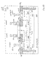
- FIGS. 1A and 1B depict schematic diagram embodiments of an SCR ESD protection device 102 of the present invention.
- Each of the embodiments in schematic diagrams A and B illustratively depicts a portion of an integrated circuit (IC) 100 having protected circuitry (functional circuitry) 101, and an SCR ESD protection device 102 coupled to a pad 104 of the protected circuitry 101.
- IC integrated circuit
- SCR ESD protection device 102 coupled to a pad 104 of the protected circuitry 101.
- the ESD protection device 102 comprises a SCR 103 coupled between the pad 104 and ground 112, with an external on-chip triggering device 105 coupled to the SCR 103.
- the triggering device 105 and SCR 103 together serve as an electrostatic discharge protection device 102 for the circuitry (i.e., functional circuitry) 101 of an integrated circuit (IC) 100.
- the SCR 103 in conjunction with the triggering device 105, protects the IC circuitry 101 from electrostatic discharges (ESD) that may occur at the pad 104 of the IC circuitry 101.
- ESD electrostatic discharges
- the SCR 103 When turned on, the SCR 103 functions as a shunt to redirect any ESD currents from the pad 104, through an anode 122 and cathode 124 of the SCR 103, to ground 112.
- the trigger device 105 turns on, that is "triggers" the SCR 103, to quickly dissipate such over-voltage ESD condition.
- the SCR protection device 102 includes a PNP transistor QP 132 and an NPN transistor QN 131.
- an anode 122 of the SCR 103 is connected to the pad 104 and optionally to a first side of a resistor R N 142.
- the resistor R N 142 is used to suppress unintended triggering at low currents.
- the anode 122 is coupled to an emitter 108 of the PNP transistor QP 132, which is parallel to the shunt resistor R N 142.
- a number of serial diodes D s may be coupled between the anode 122 and the emitter 108 of the PNP transistor QP 132.
- the serially connected diodes D S (typically 1-4 diodes) are optionally provided to increase the holding voltage of the SCR 103 as may be required to fulfill latch-up specifications.
- a first node 134 includes the base of the PNP transistor QP 132, the other side of the resistor R N 142, and the collector of a NPN transistor QN 131. Additionally, the collector of the PNP transistor QP 132 is connected to the base of the NPN transistor QN 131, as well as to one side of a resistor R P 141, which forms a second node 136. The other side of resistor R P 141 is connected to a third node 124, which is coupled to ground 112. The resistor R P 141 is used to suppress unintended triggering at low currents, such as leakage currents. Furthermore, the emitter of the NPN transistor QN 131 is also connected to the grounded third node 124 and functions as a cathode of the SCR 103.
- resistors 141 and 142 can control the total resistance to ground 112, and thus control triggering and
- any leakage currents from the trigger device 105 are shunted to ground 112 via the path through this resistor 141.
- the triggering device 105 in the schematic diagram of FIG. 1A is an external on-chip trigger device 105 that is coupled between the first node 134 and ground 112. Specifically, the trigger device 105 is coupled to the base of the PNP transistor QP 132, which is commonly designated as a second gate G2 of the SCR 103. In an alternate embodiment shown in FIG. 1B, the triggering device 105 is coupled between the pad 104 and the second node 136. Specifically, the trigger device 105 is coupled to the base of the NPN transistor QP 131, which is commonly designated as a first gate G1 of the SCR 103.
- the trigger device 105 is considered “external" to the SCR 103, since the trigger device 105 does not have any structural components that are integrated (i.e., shared by) the structural components of the SCR 103.
- a further aspect of the invention is to provide SCR triggering via various embodiments of external on-chip triggering diodes utilizing a HBT structure, as discussed with regard to FIGS. 5-9. It is noted that the triggering of the SCR is also possible by using internal trigger mechanisms such as the breakdown of the junction formed between the N- epitaxial layer and the first p-doped (p-base) region, as illustrated below in FIG. 2.
- one inventive feature of the SCR of the present invention is the structural formation comprising a lateral bipolar transistor and a vertical bipolar transistor to form the SCR 103.
- Another inventive aspect of the invention pertains to the utilization of silicon germanium (SiGe) technologies in the SCR 103 to form a vertical heterojunction bipolar transistor (HBT).
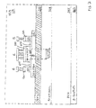
- FIG. 2 depicts a cross-sectional view of a first embodiment of a SCR ESD protection device of FIGS. 1A and 1B.
- the illustrative schematic diagram in FIG. 2 represents the components of the SCR 103, which correspond to the schematic diagram embodiments in FIGS. 1A and 1B. That is, FIG. 2 is illustrated and discussed as a SCR formed by a lateral bipolar transistor and a vertical bipolar transistor. It is noted that the trigger devices 105 are not depicted on the cross-sectional view of FIG. 2.
- the SCR protection device 103 comprises a stack of doped layers that include a P-type substrate 203, a buried N-doped layer (hereinafter referred to as a "buried layer N-type" (BLN)) 205, a N-doped layer (e.g., a lightly doped or N-epitaxial layer) 208, and at least one N+ sinker region 206.
- the SCR ESD protection device also comprises a first P doped region 214, at least one second P doped region 212, a first N+ doped poly silicon region 216, at least one second N+ doped region 210.
- N-epitaxial layer 208 is formed over the BLN 205.
- Lateral isolation of the N-epitaxial layer 208 is provided by a ring of deep trench isolation (DTI) 219. That is, a deep trench is etched around the active device region and filled with an isolating oxide, such as silicon dioxide (SiO 2 ), among others.
- DTI deep trench isolation
- Deep highly N-doped regions i.e., N+ sinker regions 206 1 and 206 2 (collectively N+ sinker regions 206) are formed proximate the DTI 219 by implanting N-type dopants having a doping concentration of about 10 18 atoms/cm -3 .
- the lightly N-doped layer 208 is formed over the BLN 205 and between the N-sinker regions 206.
- the N+ sinker regions 206 are used to form an ohmic connection from N+ diffusion regions 210 down to the BLN 205.
- Shallow trench isolation (STI) 218 is used to separate regions that are designated for formation (e.g., implantation/diffusion) of the high-doped regions (e.g., second N+ and P+ doped regions 210, 212,) as illustrated in FIG. 2.
- the high-doped regions e.g., second N+ and P+ doped regions 210, 212,
- shallow trenches are etched in specific areas, and an insulator material (e.g., silicon dioxide (SiO 2 ) and the like) is deposited in the shallow trenches.
- the regions 210 and 212 may also be separated by other techniques known in the art that are beneficial to the SCR operation, as described in commonly assigned US patent application Serial No. 10/007,833, filed November 5, 2001, which is hereby incorporated by reference in its entirety.
- the SCR 103 is preferably formed symmetrically, such that the cathode 124 is substantially centered between the two P+ regions 212 1 and 212 2 forming the anode 122, where each P+ anode region 122 is on opposing sides of the cathode 124.
- the symmetry is preferably provided as a technique to save real estate on the IC 100, and thus provide a more compact implementation and less area overhead, instead of just providing a single large P+ region 212 to serve as the anode 122. Further, the symmetry allows for more efficient geometric layouts that promote increased current flow.
- N+ and P+ implant and annealing steps are conducted following the STI region formations to form the high-doped N+ and P+ regions 210 and 212, respectively.
- the implantations are provided through separate photo masks for the N+ and P+ to allow the dopants to penetrate only into the dedicated regions of the IC 100. Referring to FIG. 4, the areas surrounding the cathode regions 216, first gate regions 226, anode regions 212, and second gate regions 210 are shown as being covered by the insulative STI material during the processing.
- the second N+ regions (N+ diffusion regions) 210 1 and 210 2 are provided over each N-sinker region 206, which form the second gate G2 134.
- the second P+ region (P+ diffusion region) 212 1 and 212 2 are provided over the N-epi layer 208 to form the anode 122.
- the STI 218 separates and electrically isolates the second N+ regions 210 from the second P+ regions 212, as well as the second P+ regions 212 from the first P+ region 214.
- the vertical NPN transistor QN 131 is formed by the first P doped region 214 formed over the N-epi layer 208 and the first N+ poly silicon region 216 formed over the first P doped region 214.
- the first N+ poly silicon region (N+ emitter) 216 and the first P doped region 214 respectively form the emitter and base of the vertical NPN transistor QN 131.
- the N-epi layer 208, N-sinker regions 206, and BLN 205 together form the collector of the vertical NPN transistor QN 131.
- the first N+ poly silicon region (emitter) 216 is typically a N+ doped poly silicon material that also forms the cathode 124 of the SCR 103.
- FIG. 3 depicts a top view of a second embodiment of the SCR ESD protection device of FIGS. 1A and 1B.
- FIG. 3 illustrates one embodiment of many possible layouts of the SCR components to conserve real estate on the IC 100 and enhance performance by minimizing the SCR transistor base widths. Many aspects shown in FIG. 3 may be applied to the embodiments depicted in FIGS. 2 and 4 herein.
- the cathode 124 is formed by a plurality of the first N+ poly silicon regions (e.g., 216 1 through 216 3 , collectively N+ regions 216), which are linearly interspersed over the first P doped region 214.
- the trigger gate G1 formed by the P+ poly silicon regions 226 are interspersed and aligned with the plurality of second N+ poly silicon regions 216 over the first P doped region 214.
- the anode 122 may be formed by a plurality of the second P+ poly silicon regions (not shown), which are linearly interspersed over the N-epi layer 208.
- the trigger gate G2 which is formed by the second N+ doped region 210, may also comprise a plurality of second N+ doped regions (not shown) that are interspersed and aligned with the plurality of second P+ poly silicon regions over the N-epi layer 208.
- the lateral PNP transistor QP 132 is formed by at least one second P+ doped region (e.g., 212 1 and 212 2 , collectively 212), the N-epi region 208 collectively with the BLN 205, and the first P doped region 214.
- the second P+ doped region 212, the N-epi region 208 collectively with the BLN 205, and the first P doped region 214 respectively form the emitter, base, and collector of the lateral PNP transistor QP 132.
- the second P+ doped region 212 is typically a P+ doped poly silicon material, however, in an alternative embodiment, the second P+ doped region 212 is fabricated from a P+ doped SiGe material, as discussed below in further detail.
- the first P doped region 214 serves dual functions as forming the collector of the lateral PNP transistor QP 132, as well as the base of the vertical NPN transistor QN 131.
- the N-epi layer 208 and the BLN 205 collectively serve dual functions as forming the collector of the vertical NPN transistor QN 131, as well as the base for the lateral PNP transistor QP 132.
- the first gate G1 136 is formed by at least one P+ base poly silicon region 226, which is respectively disposed over first P doped region 214.
- the first gate 136 illustratively comprises a plurality of P+ base poly regions (e.g., regions 226 1 and 226 2 ) located on opposing sides of the first N+ cathode poly silicon region 216.
- the first gate regions 226 1 and 226 2 are respectively disposed proximate and between each of the plurality of first N+ emitter poly silicon regions 216. That is, the first gate regions 226 1 and 226 2 are respectively disposed between the first N+ emitter regions 216 1 and 216 2 , as well as between the first N+ emitter poly silicon regions 216 2 and 216 3 .
- first gate regions 226 in line with the N+ emitter/cathode poly silicon regions 216 allows the anode regions (i.e., second P+ doped regions 212) to be placed closer to the cathode such that the lateral dimensions L N may be reduced for faster turn-on of the SCR 103, as discussed below in further detail with regard to FIG. 2.
- Insulative regions 224 1 and 224 2 isolate the first N+ emitter poly silicon region 216 from the P+ base poly silicon regions 226 of the first gate 136.
- the insulative regions 224 1 and 224 2 are disposed over the first P doped region 214 and between the first N+ emitter poly silicon region 216 and the P+ poly silicon regions 226 1 and 226 2 .
- the first N+ emitter poly silicon region 216 is also formed over a portion of the insulative regions 224 1 and 224 2 .
- the portion of the first N+ emitter poly silicon region 216 positioned between the insulative regions 224 1 and 224 2 define a window (i.e., "emitter opening") 230 therebetween, as is discussed in further detail below.
- a silicide layer 220 is formed over the first N+ poly silicon region 216 (cathode), the first gate regions 226 (G1), the second gate regions, 210 (G2), and the second P+ regions 212 (anode).
- a metal layer e.g., using cobalt, titanium, and the like
- a highly conductive alloy is formed between the metal and the silicon (“silicide").
- the silicide layers 220 serve as a conductive bond between the high-doped regions (216, 210, 212, and 226) and their respective metal contacts, which provide external connectivity at the anode 122, cathode 124, first gate 136, and second gate 134 of the SCR 103.
- ILD 250 oxide layers known as Inter-Level Dielectric (ILD) 250 (drawn in phantom) are deposited over the doped regions. An etching process is performed to form the contact holes, which are subsequently filled with metal to form the metal contacts. Several contact holes may be placed in rows over the emitter opening 230 to increase the maximum current. It is noted that that the total number of contact holes over the anode 122 (i.e., second P+ regions 212) approximately matches the number of contact holes in the cathode 124 (i.e., first N+ poly silicon region 216).
- all of the P and N-type regions are formed from a silicon-only lattice structure.
- the first and second doped regions 214 and 212 have a doping concentration of about 10 21 atoms/cm -3 .
- the first N+ poly silicon region (emitter) 216 and second N+ region (second gate) 210, as well as the P + poly silicon regions 226, have doping concentrations of about 10 21 atoms/cm -3 .
- the BLN layer 205 has a doping concentration of about 10 19 atoms/cm -3
- the N+ sinker region 206 has a doping concentration of about 10 20 atoms/cm -3
- the N- epitaxial layer 208 has a doping concentration in the range of 10 16 to 10 17 atoms/cm -3 , which is the lowest doping concentration of the protection device 103.
- the first P doped region 214 comprises a silicon germanium (SiGe) lattice structure.
- the first P doped region 214 is formed from silicon and Germanium.
- the concentration is gradually increased with the depth of the layer from 0% to up to a peak concentration of approx. 10-13%.
- the silicon concentration reduces respectively from 100% down to approx. 90-87%.
- the SiGe is doped with Boron at a concentration of about 10 19 atoms/cm -3 .
- the remaining layers and regions of the protection device 102 are the same as discussed above.
- the utilization of the silicon germanium lattice structure is particularly suited for circuitry operating under RF applications, such as wireless chips and devices.
- the implementation of the SiGe HBT i.e., vertical NPN transistor 131 has a very low junction capacitance, which makes the SCR suitable for the high (RF) frequencies, since the parasitic junction capacitance of the SCR 103 may be minimized by having a low junction capacitance while providing a very high level of ESD hardness.
- the junction area between the base and collector i.e., SiGe P doped region 214 and the N-epi region 208 region is defined by the emitter opening, and therefore is minimized.
- the N-epi layer 208 (collector) is very lightly doped as compared to a standard non-epi semiconductor processes.
- the typical junction capacitance is 0.7 femto Farad per square-micron area (compared to 1.6 femto Farad per square-micron for P+/N-well per square-micron area).
- parasitic capacitances such as the one between the BLN and the P-substrate or at the sidewalls (DTI) of the device, all capacitance values have been already minimized to meet the high frequency requirement for the functional HBT devices.
- the first and second P doped regions 214 and 212 are each fabricated from SiGe, and are doped with Boron at a concentration of about 10 19 cm -3 .
- the joint formation of the first and second P doped regions 214 and 212 allows for easier fabrication processing, thereby reducing costs.
- the performance of this third embodiment is substantially the same as the second embodiment in which the second P doped region 212 is formed from only a silicon-based lattice structure.
- One objective of the present invention is to increase the speed in which the SCR 103 turns on. Decreasing the turn on time of the SCR 103 is realized by two particular differences over SCRs 103 that are formed by a pair of lateral bipolar transistors in the prior art.
- One difference over the prior art is a reduction in the size of the respective base regions of the transistors QN 131 and QP 132 in the SCR 103, which influences the turn on time of the SCR 103, as well as the current gains ⁇ of the transistors 131 and 132.
- the increased transistor current gains ⁇ help ensure that enough current is provided to forward bias the bases of each transistor QN 131 and QP 132, and thereby quickly and reliably activate the SCR 103.
- the dimensions L P and L N represent the respective base lengths of the vertical NPN transistor QN 131 and the lateral PNP transistor QP 132.
- the base length L P of the NPN transistor QN 131 is in the range of 15-50 nm.
- the base length L N is measured from the edge 211 of the second P+ region 212 to the emitter opening 230.
- the emitter opening 230 is defined as the N-epi region located below the first P+ region 214 that is not covered by the insulative material (e.g., SiO 2 ) 224.
- the size of the emitter opening 230 determines the cross-section for the current flow.
- the base length L N of the PNP transistor QP 132 is in the range of 1.0 to 2.0 microns.
- the SCR turn-on time is related to the combined turn-on times of the each transistor QN 131 and QP 132.
- the turn-on times of the bipolar transistors 131 and 132 are proportionally related to the square of their respective base widths. Accordingly, since the base width (L P ) of the NPN bipolar transistor has been reduced by virtue of implementing the vertical NPN transistor QN 131, the turn on time of the SCR has also been greatly reduced as compared to an SCR having a pair of laterally formed transistors.
- the SiGe heterojunction transistor allows for control of the electrons and holes independently.
- the overall gain-bandwidth product (f max ) which characterizes the maximum frequency of operation, may be improved.
- the overall gain-bandwidth product (f max ) may be improved by two fabrication methods. The first fabrication method is to provide a high germanium concentration in a uniform base, while a second method is to provide a low germanium concentration in a graded base.
- the resistivity in the base layer is greatly reduced.
- the heterojunction at the base-emitter interface of the NPN transistor QN 131 reduces hole injection into the emitter, such that the current gain remains high.
- the speed of the device, as measured by the emitter-collector transit time is equivalent to that of a conventional bipolar transistor, but the gain-bandwidth product is greatly increased due to the large reduction in base spreading resistance.
- This first fabrication method is most suitable for power applications.
- the germanium In the second fabrication method (low germanium concentration in a graded base), the germanium varies from very low concentration at the emitter-base junction to around 10% at the collector-base junction of the NPN transistor QN 131. In this case, the current gain is only slightly affected. However, the speed of the device, as measured by the emitter-collector transit time, is increased due to a built-in field generated by the Germanium concentration gradient across the base. Moreover, the base-width modulation (modulation of the base-collector depletion layer width caused by variations in the collector-base voltage) is diminished, however the high current gain fall-off is increased due to the heterojunction at the collector-base interface. Accordingly, this second fabrication method is most suitable for small signal applications. The latter technique has the drawback of a higher resistivity in the base layer. Therefore, the ESD capability in the mentioned prior art devices is relatively low.
- FIG. 4 depicts a cross-sectional view of a third embodiment of a SCR ESD protection device of FIGS. 1A and 1B.
- the embodiment shown in FIG. 4 is the same as the embodiment of FIG. 2, except that the BLN 205 and N+ sinker regions are omitted, and an N-well 406 is formed over the N-epi layer 208.
- the N-epitaxial layer 208 is formed over the P-substrate 203, and the N-well 406 is diffused into the N-epi layer 208 and laterally isolated by the DTI 219.
- the N-well 406 has an N-doping concentration of about 10 18 atoms/cm -3 , which is less than the BLN 205,
- the first P doped region 214, second P doped regions 212, second N+ doped regions 210, and first N+ doped region 216 are formed over the N-well 406 as discussed above with regard to FIG. 2.
- the first and second P doped regions 214 and 212 may comprise only silicon doped material, or SiGe, as also discussed above with regard to FIG. 2.
- the omission of the BLN 205 and inclusion of the N-well 406 prevents any possible deterioration of the current gain in the distributed lateral PNP transistor QP 132 of the SCR 103.
- the deterioration of the current gain which is due to the high doping concentrations of the BLN 205, may offset the advantages of having a low resistive current path through the BLN 205.
- the diffused N-well 406 forms the base of the lateral PNP transistor 132 (as well as the collector of the vertical NPN transistor 132), with minimal reduction in current gain ⁇ .
- an asymmetric layout may also be implemented.
- a single second P+ doped region 212 e.g., 212 1
- a single second N+ doped region 210 forming the first gate and a single P base poly region 226 forming the second gate.
- the anode 122 defined by the P+ region 212 1 is larger than the symmetrical embodiment, since the number of contact holes in the anode 122 must substantially match the number of contact holes in the cathode 124.
- the DTI ring of insulative material is formed under the STI region approximately where the second P+ base poly silicon region 226 2 is formed.
- ESD protection performance of an asymmetrical SCR of the present invention is comparable with regard to current gain and SCR turn-on time as to the performance of the preferred symmetrical SCR layout.
- the SCR of the present embodiments provide a vertical NPN transistor QN 131 with a distributed (i.e., lateral) PNP transistor QP 132.
- the vertical NPN transistor has reduced base length L P and vertical current flow from the emitter to the collector, which increases the current gain, current flow, and turn-on time, as compared to a SCR having distributed (i.e., lateral) NPN and PNP transistors.
- the SCR 103 is vertically isolated from the P-substrate 203 by the a reverse diode formed by the BLN 205 and P-substrate 203 junction, as well as laterally by the DTI 219. Accordingly, the SCR 103 may be used as an ESD protection device in various situations usually encountered for ICs used in RF applications, such as wireless devices. In such RF circuits, signals may swing above the positive supply voltage or below the negative supply voltage. Protection devices that are isolated from the P-substrate 203 are beneficial in both instances, since only they can comply with the circuit requirement that no conductive path opens to the supply or ground line if such an overshoot or undershoot of the signal occurs.
- the gates may be omitted completely, or only a single gate or both gates (i.e., gate G1 or G2) may be required based upon the circuitry of the IC 100 to be protected.
- gate G1 or G2 only the second gate G2 136 is used to trigger the SCR 103 when protecting against an ESD event occurring at the pad 104.
- the P+ poly silicon base regions 226 that form the first gate G1 would not be required.
- Utilizing only the second gate G2 134 avoids any potential heating issues that may occur by using the first gate G1 136, due to lateral (trigger) current flow through the SiGe base 214 of the NPN transistor 131.
- the first gate G1 134 is used to trigger the SCR 103.
- the N+ regions 210 and N+ sinker regions 206 that form the second gate G2 would not be required. Eliminating an unused gate provides for a more compact layout of the ESD protection device 102.
- the trigger gate G1 136 is a short and direct way of injecting the trigger current into the highly effective HBT base region, as well as lessening the trigger speed of the SCR 102 as compared with using the second gate G2 134 to trigger the lateral PNP transistor 132.
- both gates G1 and G2 134 and 136 may also be implemented to provide connectivity to independent triggering devices 105. Specifically, there are instances where each gate may be used to trigger the SCR 103 and protect against different types of ESD events. Such ESD events may include positive or negative ESD events occurring at a particular pad, ESD events occurring at different components of the functional circuitry 101, among others.
- the trigger gates may be eliminated entirely. Elimination of both gates allows for a more compact IC layout because the N+ sinker region 506, the N+ G2 region 510, and the P+ base poly silicon 522 are no longer required. Omission of both gates G1 and G2 is applicable where the trigger voltage of the SCR can be determined by the avalanche breakdown of the heterojunction between the N-epi and the P-base layer (SiGe).
- FIGS. 5A and 5B depict cross-sectional views of a first embodiment of a diode trigger device 105.
- the SCR is turned on (i.e., "triggered") by an extemal on-chip trigger device 105.
- the trigger device 105 is external to the SCR, since neither the SCR 103 nor the trigger device 105 has any integrated or shared components.
- the triggering devices discussed in FIGS. 5-9 are utilized for SCR embodiments utilizing the SiGe lattice structure in the first P doped region 214. That is, the trigger devices 105 of FIGS. 5-9 may be used in instances where the vertical NPN transistor 131 is a heterojunction bipolar transistor (HBT).
- HBT heterojunction bipolar transistor
- the exemplary triggering device 105 (of both FIGS. 5A and 5B) is a heterojunction diode (HBD) triggering device 105 that utilizes a collector (C) to base (B) breakdown of the heterojunction transistor (HBT).
- the HBD trigger device 105 comprises a stack of doped layers that include a P-type substrate 203, a buried N-doped layer (hereinafter referred to as a "buried layer N-type" (BLN)) 505, an N-epitaxial layer 508, and at least one N+ sinker region 506, as discussed above with regard to the SCR 103.
- the HBD trigger device 105 also comprises a SiGe doped region 514, at least one N+ diffusion region 510, and at least one P+ poly base region 522.
- the structure of the trigger device 105 is similar in many aspects to the structure of the SCR 103.
- the silicon P-substrate 203 is formed the highly conductive BLN 505.
- the N-epitaxial layer 508 is formed over the BLN 205.
- Lateral isolation of the N-epi layer 508 is provided by a ring of deep trench isolation (DTI) 519, such as silicon dioxide (SiO 2 ), among others.
- DTI deep trench isolation
- N+ sinker regions 506 1 and 506 2 Deep highly N-doped regions (i.e., N+ sinker regions 506 1 and 506 2 (collectively N+ sinker regions 506) are formed proximate the DTI 519 by implanting N-type dopants as discussed above with regard to the SCR 103. As such, the N-epi layer 508 is formed over the BLN 205 and between the N+ sinker regions 506. The N+ sinker regions 506 are used to form a low-ohmic connection from N+ diffusion regions 510 down to the BLN 505.
- Shallow trench isolation (STI) 518 is used to separate regions that are designated for formation (e.g., implantation) of the high-doped regions (e.g., N+ diffusion region 510 and SiGe P-doped region 514) as discussed above with regard to the SCR 103.
- STI Shallow trench isolation
- N+ implant and annealing steps are conducted following the STI region formations to form the high-doped N+ regions 510.
- the N+ diffusion regions 510 1 and 510 2 are provided over each N+ sinker region 506, which form the cathode 532 (equivalent to the collector contact of the HBT)) of the heterojunction diode.
- STI regions 518 1 and 518 2 isolate N+ diffusion region 510 1
- STI regions 518 3 and 518 4 isolate N+ diffusion region 510 2
- N-epi layer region 509 is maintained between STI regions 518 2 and 518 3
- the SiGe P doped region 514 is broadly deposited over the N-epi layer region 509 and adjacent STI regions 518 2 and 518 3 .
- the P+ base poly silicon region 522 is formed over the P doped region 514, which collectively form the anode 534 (equivalent to the base contact of the HBT) of the HBD 105.
- the P+ base poly silicon region 522 is centered over the P doped region 514 and N-epi layer 508. That is, the anode 534 has direct contact over the active SiGe P doped region 514.
- the P+ base poly silicon region 522 is divided into two regions 522 1 and 522 2 with each P+ base poly silicon region 522 formed laterally on the P doped region 514 and over the STI 518 formed beneath the SiGe P doped region 514. That is, the anode 534 has indirect contact to the active junction, since the P base poly silicon regions 522 1 and 522 2 are placed lateral to the active SiGe P doped region 514.
- the high-doped regions N+ diffusion and P+ base poly silicon regions 510 and 522) may optionally be silicided 520, as discussed above with regard to the SCR 103.
- the SiGe P doped region (base) 514 forms the anode of the HBD 105, while the N+ diffusion regions 510 1 and 510 2 , N+ sinker regions 506 1 and 506 2 , and N-epi layer 508 collectively form the cathode of the HBD 105.
- the highly doped BLN 505, N+ sinker regions 506, and N+ diffusion regions 510 ensure that there is a low-resistive connection to the cathode terminal 532.
- the reverse breakdown of the trigger diode 105 occurs at the P-N junction between the SiGe P-base and the N-epi layer region 509 disposed thereunder.
- the breakdown voltage of the HBD is in a range between 6 and 9 volts.
- junction capacitance is very low because the N-epi layer 508 is lightly doped (e.g., doping concentration around 10 16 to 10 17 atoms/cm -3 ).
- the low level doping in the N-epi layer 508 allows the depletion layer of the diode to extend further into the silicon of the N-epi layer. A longer depletion layer width results in lower junction capacitance.
- an N-well region 507 (drawn in phantom) is formed in the N-epitaxial layer 508, Specifically, the N-well 507 is formed beneath the SiGe P doped region 514. In particular, the N-well 507 extends laterally between the DTI regions 519 beneath the N+ diffusion regions 510. Accordingly, the N+ sinker regions 506 are no longer required.
- the N-well 507 is provided to further lower the trigger voltage by increasing the doping concentration (e.g., 10 18 atoms/cm -3 ) at the N-side of the junction. A higher doping concentration causes a shorter depletion layer width in which the voltage drops with higher electric field strength. The latter leads to a higher avalanche multiplication factor and a lower breakdown voltage.
- FIGS. 8A-8C depict exemplary schematic diagram embodiments of the trigger devices illustrated in FIGS. 6 and 7.
- each schematic drawing shows the trigger device 105 coupled to the SCR that collectively form the ESD protection device 102 that protects functional circuitry 101 on the IC 100.
- an external on-chip resistor 802 is coupled from the triggering device 105 at node 136 to ground 112.
- FIG. 6 depicts a cross-sectional view of a second embodiment of a trigger device 105 of the present invention.
- FIG. 8A illustrates a collector-base diode of the heterojunction bipolar transistor HBT105 with a shorted base-emitter.
- FIG. 8B illustrates a collector-emitter device with an open base.
- the structure shown in FIG. 6 may be used in either configuration shown in FIGS. 8A and 8B, depending on how the base terminal is externally connected.
- FIG. 6 depicts a trigger device 105 for a SiGe SCR utilizing the collector-emitter breakdown of a heterojunction bipolar transistor (HBT).
- FIG. 6 is structurally the same as depicted in FIG. 5B, except that an N+ emitter region 602 is formed over the SiGe P doped region 514 and between the P base poly silicon regions 522 1 and 522 2 . More specifically, insulative layers 624 are formed between the N+ emitter region 602 and the P base poly silicon regions 522 1 and 522 2 . As such, an emitter opening 630 is defined beneath the N+ emitter region 602 and within the edges of the insulative layers 624, as discussed above with regard to the SCR 103.
- HBT heterojunction bipolar transistor
- N+ emitter region 602 provides an intrinsically more robust trigger element because of the internal current amplification, as well as the vertical current flow from the emitter to the collector. It is noted that the collector is tied to the higher potential in the ESD protection circuit, while the base and emitter are both coupled to a lower potential (e.g., gate G1 136) of the HBT SCR 103.
- an N-well 604 (drawn in phantom) is provided in a similar manner as described in regard to FIGS. 5A and 5B.
- the N-well 604 is provided inside the N-epi layer 508 to further lower the trigger voltage by increasing the doping concentration (e.g. 10 18 atoms/cm -3 at the N-side of the junction in the same manner as discussed with respect to FIGS. 5A and 5B.
- the structure shown in FIG. 6 may have the base externally coupled to the emitter (FIG. 8A) or floating (FIG. 8B).
- the advantage of the structures having the emitter connected (FIG. 8A and 8B) over the structure with collector-base breakdown (FIG. 5A and 5B) is a more robust trigger device, as discussed earlier. Shorting the base-emitter (FIG. 8A) results in a breakdown and thus a triggering voltage for the ESD protection device 102 of typically 6 to 9 Volts.
- a floating base (FIG. 8B) results in a lowered breakdown voltage of typically 4 to 7 Volts.
- the proper version (FIG. 8A or 8B) may be selected.
- FIG. 7 depicts a cross-sectional view of a second embodiment of a trigger device 105 of the present invention
- FIGS. 8C illustrates an emitter-base diode with an open collector, as shown in FIG 7.
- the emitter-base diode trigger device 105 is a SiGe SCR utilizing the base-emitter breakdown of the heterojunction bipolar transistor (HBT).
- the BLN 505 and N-epitaxial layer 508 are disposed over the P-substrate 203, as discussed above with regard to the other trigger device embodiments of FIGS. 5 and 6.
- the SiGe P-base layer 514 is formed over the N-epi layer 508, however an insulative material provided during formation of the STI 518 is formed over the N-epi layer 508, thereby isolating the SiGe P-base layer 514 from the N-epi layer 508.
- the base to collector junction of the HBT is omitted from the trigger device 105.
- the trigger device 105 comprises the base-emitter diode formed between the N+ emitter region 602 and the SiGe P-base layer 514.
- the embodiment of FIG 7 has breakdown voltage that is lower than any of the embodiments in FIGS. 5A, 5B, 6, 8A, and 8B.
- the low breakdown voltage of FIG 7 is due to the heterojunction formed by the highly P doped SiGe base region 514 and the again highly doped N+ emitter region 602. As discussed above, an increase in the doping levels reduces the breakdown voltage.
- the emitter to base breakdown voltage of the trigger device of FIG. 7 is typically in a range between 4 and 6 Volts.
- Providing an SCR 103 with a structural formation including a vertical NPN transistor 131 in conjunction with a lateral PNP transistor decreases the turn-on time of the SCR 103. Specifically, the SCR performance improves due to the high current that flows in the vertical NPN transistor 131, as compared to a SCR having a distributed (i.e., lateral) NPN transistor. Moreover, fabricating the base of the vertical NPN transistor 131 using a Silicon-Germanium lattice allows the SiGe SCR 103 to be used in high frequency applications, such as wireless devices. In particular, the P-doped SiGe base provides an extremely low junction capacitance to the low-doped N-epi collector region underneath it, which is well suited for RF applications.
- the triggering devices 105 may also be fabricated using the SiGe technologies. Specifically, a heterojunction diode is coupled to a gate of the SCR, such that the reverse breakdown voltage of the heterojunction diode defines the trigger voltage to the SCR. Although the heterojunction triggering devices are preferred for high frequency applications, one skilled in the art will appreciate that other triggering devices may be coupled to the SCR 103 of the present invention to trigger the SCR.
- the HBD devices in FIGS. 5A, 5B, 6, and 7 have been discussed in terms of being used as trigger devices for the ESD-SCR.
- the HBD devices may also be used as ESD protection devices by themselves. That is, the diodes can be applied to shunt an ESD pulse having the 'opposite polarity'. Opposite polarity means that the pad connected to the protected circuitry receives a negative ESD pulse with respect to ground. In this case, the diode (and not the e.g. SCR) will provide the conductive path to safely discharge the ESD event.
- FIG. 9 depicts a schematic diagram of the SCR ESD protection device of FIG. 1B coupled to a shunt diode 902.
- FIG. 9 illustrates the use of a shunt diode 902 to shunt an ESD pulse having the opposite polarity.
- the schematic drawing of FIG. 9 is the same as the schematic drawing of FIG. 1B, such that the triggering device 105 is a diode, and the shunt diode 902 is coupled to the anode 122 of the SCR 103 as well as the pad 104, and to ground 112.
- the cathode of the trigger diode 105 is coupled to ground 112 via the resistor 141, while the anode of the trigger diode 105 is coupled to the pad 104.
- the cathode of the shunt diode 902 is coupled directly to ground 112, while the anode of the shunt diode is coupled to pad 104.
- FIG. 9 A preferred embodiment for this type of application in FIG. 9 is the HBD device 500, as shown in Fig. 5A.
- the embodiment shown in FIG. 5A illustrates a direct anode (base) contact providing the lowest possible forward on-resistance, which makes it most suitable as shunt element.
- the direct anode (base) contact of FIG. 5A allows maximum current flow at the heterojunction, as opposed to the prior art devices that utilize indirect anode (base contact), which restricts current flow there through.
- the other HBD diodes as shown in Fig. 5B, 6, and 7 may also be used as ESD shunt devices, however these embodiments are better suited as triggering devices for the SCR.
- These other HBD diodes provide lower performance due to the higher resistance and lower current capability, however, as trigger devices they benefit from a typically lower breakdown voltage.
Abstract
Description
- This invention generally relates to the field of electrostatic discharge (ESD) protection arrangements, and more specifically, to silicon controlled rectifier (SCR) structures useful in ESD protection circuitry.
- Technologies utilizing high frequency signals, such as the mobile telephone and other wireless devices, are currently incorporating silicon germanium (SiGe) into the integrated circuits (ICs). The silicon germanium technology gives the chip manufacturers the ability to satisfy the analog/RF design requirements, such as transistor speed, while maintaining a high transistor current gain. The introduction of a SiGe layer over a silicon layer (e.g., N-epitaxial layer) forms a heterojunction therebetween. Accordingly, a heterojunction bipolar transistor (HBT) may be formed and integrated with functional circuitry, e.g., complimentary metal oxide semiconductor (CMOS) circuitry, on a chip. That is, the HBTs are used as functional RF circuitry, where the SiGe layer allows for producing high-speed transistors, which may be used for RF applications.
- Semiconductor devices, such as IC's having the SiGe HBT transistors are sensitive to the high voltages that may be generated by contact with an ESD event. As such, electrostatic discharge (ESD) protection circuitry is essential for integrated circuits. An ESD event commonly results from the discharge of a high voltage potential (typically, several kilovolts) and leads to pulses of high current (several amperes) of a short duration (typically, 100 nanoseconds).
- Recent studies have shown that functional heterojunction bipolar transistors also have some intrinsic ESD protection capabilities. For example, in one publication, it was shown that a functional HBT, without any additional ESD protection circuitry, was found to have measurable intrinsic ESD protection characteristics, as between two transistor terminals (e.g., base-collector, base-emitter, and the like). For a detailed understanding of one such study, the reader is directed to the publication entitled "Electrostatic Discharge Characterization of Epitaxial-Base Silicon-Germanium Heterojunction Bipolar Transistors" by S. Voldman et al., Electrical Overstress/Electrostatic Discharge Symposium Proceedings 2000, EOS-22, pp.239-250, IEEE Catalog No. OOTH8476, ISBN-1-58537-018-5.
- However, the intrinsic ESD protection capabilities of a functional heterojunction bipolar transistor are limited, such that ESD protection (voltage clamping and current capability) for the functional circuitry may not be adequately provided. For example, an emitter-base junction can handle only very limited ESD current until a destructive failure occurs. One reason is that the ESD stress current has to flow from the base contact to the active base-emitter junction. Therefore, the current will flow in the extremely thin (e.g., 50 nanometers) layer of the SiGe that is connecting the base contact to the active transistor region. This leads to an early failure, as well as a significant voltage build-up at the device terminals, which makes the device unpractical for any ESD application, for example, of protecting RF receiver inputs where the base of the HBT is connected to the input terminal while the emitter is grounded.
- An additional reason for such low current ESD failures may also be attributed to the long and narrow base poly-crystalline silicon connections that become necessary in practical RF transistor layout. Along these base poly-crystalline silicon connections, resistance is increases, while the voltage drops during ESD, which is not permissible. Therefore, there is a need in the art for improved ESD protection devices in semiconductor technologies utilizing silicon-germanium technologies.
- Various respective aspects and features of the invention are defined in the appended claims. Features from the dependent claims may be combined with features of the independent claims as appropriate and not merely as explicitly set out in the claims.
- The disadvantages heretofore associated with the prior art are overcome or at least alleviated by the present invention of an electrostatic discharge (ESD) protection device having a silicon controlled rectifier (SCR) for protecting circuitry of an integrated circuit (IC). The SCR comprises a vertical NPN transistor and a lateral PNP transistor.
- In one embodiment, an N-doped (e.g., lightly doped or N-epitaxial) layer is disposed over a substrate and a first P doped region disposed over the N-epitaxial layer. A first N+ doped region is disposed over the P-doped region and coupled to ground. The first N+ doped region, first P-doped region, and N-epitaxial layer form the vertical NPN transistor of the SCR, where the first N+ doped region forms the cathode of the SCR.
- A second P doped region is coupled to a protected pad. The second P doped region forms an anode of the SCR, and is disposed over the N-epitaxial layer and laterally positioned with respect to the first P doped region and electrically isolated from the first P doped region. The second P doped region, N-epitaxial layer, and first P doped region form the lateral PNP transistor of the SCR. A triggering device may be coupled to a gate of the SCR. For example, an external on-chip triggering device may be coupled to the gate of the SCR, where the triggering device resides on the same IC, but the triggering device does not share any components with the SCR. Alternatively, an integrated triggering device may be coupled to the gate of the SCR, where the triggering device resides on the same IC, as well as shares at least one component with the SCR.
- In one embodiment, the first P-doped region is fabricated from a silicon-germanium (SiGe) lattice. As such, the vertical NPN transistor is a heterojunction bipolar transistor (HBT), which has low junction capacitance between the base (SiGe layer) and the collector (N-epi Si). An SCR incorporating a vertical HBT of the present invention is suitable for protecting circuitry operating under high frequency applications, such as circuitry in wireless devices.
- The invention will now be described by way of example with reference to the accompanying drawings, throughout which like parts are referred to by like references, and in which:
- FIGS. 1A and 1B depict schematic diagram embodiments of an SCR ESD protection device of the present invention;
- FIG. 2 depicts a cross-sectional view of a first embodiment of the SCR ESD protection device of FIGS. 1A and 1B;
- FIG. 3 depicts a top view of a second embodiment of the SCR ESD protection device of FIGS. 1A and 1B;
- FIG. 4 depicts a cross-sectional view of a third embodiment of the SCR ESD protection device of FIGS. 1A and 1B;
- FIGS. 5A and 5B depict cross-sectional views of a first embodiment of a trigger device of the present invention;
- FIG. 6 depicts a cross-sectional view of a second embodiment of a trigger device of the present invention;
- FIG. 7 depicts a cross-sectional view of a third embodiment of a trigger device of the present invention;
- FIGS. 8A-8C depict schematic diagram embodiments of the trigger devices illustrated in FIGS. 6 and 7; and
- FIG, 9 depicts a schematic diagram of the SCR ESD protection device of FIG. 1B coupled to a shunt diode.
-
- To facilitate understanding, identical reference numerals have been used, where possible, to designate identical elements that are common to the figures.
- The process steps and structures described below do not form a complete process flow for manufacturing integrated circuits (ICs). Rather, since the present invention can be practiced in conjunction with integrated circuit fabrication techniques currently used in the art, a portion of the commonly practiced process steps is included as necessary to assist in understanding of the present invention. The figures representing cross-sections and layouts of portions of an IC during fabrication are not drawn to scale, but instead are drawn to illustrate the various features of the invention. Furthermore, where possible, the figures illustratively include a schematic diagram of the circuitry (e.g., an SCR circuit) as related to the P and N-type doped regions of the integrated circuit.
- FIGS. 1A and 1B depict schematic diagram embodiments of an SCR ESD protection device 102 of the present invention. Each of the embodiments in schematic diagrams A and B illustratively depicts a portion of an integrated circuit (IC) 100 having protected circuitry (functional circuitry) 101, and an SCR ESD protection device 102 coupled to a
pad 104 of theprotected circuitry 101. Although asingle pad 104 and SCR ESD protection device 102 is illustratively shown in the schematic drawings, one skilled in the art will appreciate that additional ESD protection devices 102 may be coupled to other pads (e.g., I/O pads) 104 for thefunctional circuitry 101 of theIC 100, as required. - The ESD protection device 102 comprises a
SCR 103 coupled between thepad 104 andground 112, with an external on-chip triggering device 105 coupled to theSCR 103. Thetriggering device 105 and SCR 103 together serve as an electrostatic discharge protection device 102 for the circuitry (i.e., functional circuitry) 101 of an integrated circuit (IC) 100. In particular, theSCR 103, in conjunction with the triggeringdevice 105, protects theIC circuitry 101 from electrostatic discharges (ESD) that may occur at thepad 104 of theIC circuitry 101. When turned on, theSCR 103 functions as a shunt to redirect any ESD currents from thepad 104, through ananode 122 andcathode 124 of theSCR 103, toground 112. Thetrigger device 105 turns on, that is "triggers" theSCR 103, to quickly dissipate such over-voltage ESD condition. - It is noted that the configuration of the
SCR 103, with regard to thepad 104,ground 112, and the protectedcircuitry 101 is the same for both embodiments shown in FIGS. 1A and 1B. Only the coupling of the triggeringdevice 105 to theSCR 103 differs between the schematic diagrams of FIGS. 1A and 1B. - Referring to the exemplary schematic diagram of FIG. 1A, the SCR protection device 102 includes a
PNP transistor QP 132 and anNPN transistor QN 131. Specifically, ananode 122 of theSCR 103 is connected to thepad 104 and optionally to a first side of aresistor R N 142. Theresistor R N 142 is used to suppress unintended triggering at low currents. Additionally, theanode 122 is coupled to anemitter 108 of thePNP transistor QP 132, which is parallel to theshunt resistor R N 142. Optionally, a number of serial diodes Ds (not shown) may be coupled between theanode 122 and theemitter 108 of thePNP transistor QP 132. The serially connected diodes DS (typically 1-4 diodes) are optionally provided to increase the holding voltage of theSCR 103 as may be required to fulfill latch-up specifications. - A
first node 134 includes the base of thePNP transistor QP 132, the other side of theresistor R N 142, and the collector of aNPN transistor QN 131. Additionally, the collector of thePNP transistor QP 132 is connected to the base of theNPN transistor QN 131, as well as to one side of a resistor RP 141, which forms asecond node 136. The other side of resistor RP 141 is connected to athird node 124, which is coupled toground 112. The resistor RP 141 is used to suppress unintended triggering at low currents, such as leakage currents. Furthermore, the emitter of theNPN transistor QN 131 is also connected to the groundedthird node 124 and functions as a cathode of theSCR 103. - Those skilled in the art will appreciate that the
resistors 141 and 142 can control the total resistance toground 112, and thus control triggering and - holding current of the
SCR 103. Furthermore, any leakage currents from thetrigger device 105 are shunted to ground 112 via the path through this resistor 141. - The triggering
device 105 in the schematic diagram of FIG. 1A is an external on-chip trigger device 105 that is coupled between thefirst node 134 andground 112. Specifically, thetrigger device 105 is coupled to the base of thePNP transistor QP 132, which is commonly designated as a second gate G2 of theSCR 103. In an alternate embodiment shown in FIG. 1B, the triggeringdevice 105 is coupled between thepad 104 and thesecond node 136. Specifically, thetrigger device 105 is coupled to the base of theNPN transistor QP 131, which is commonly designated as a first gate G1 of theSCR 103. In either embodiment, thetrigger device 105 is considered "external" to theSCR 103, since thetrigger device 105 does not have any structural components that are integrated (i.e., shared by) the structural components of theSCR 103. A further aspect of the invention is to provide SCR triggering via various embodiments of external on-chip triggering diodes utilizing a HBT structure, as discussed with regard to FIGS. 5-9. It is noted that the triggering of the SCR is also possible by using internal trigger mechanisms such as the breakdown of the junction formed between the N- epitaxial layer and the first p-doped (p-base) region, as illustrated below in FIG. 2. - Various embodiments depicting the structure and doping materials of the SCR are shown and discussed with regard to FIGS. 2-4. For example, one inventive feature of the SCR of the present invention is the structural formation comprising a lateral bipolar transistor and a vertical bipolar transistor to form the
SCR 103. Another inventive aspect of the invention pertains to the utilization of silicon germanium (SiGe) technologies in theSCR 103 to form a vertical heterojunction bipolar transistor (HBT). - FIG. 2 depicts a cross-sectional view of a first embodiment of a SCR ESD protection device of FIGS. 1A and 1B. The illustrative schematic diagram in FIG. 2 represents the components of the
SCR 103, which correspond to the schematic diagram embodiments in FIGS. 1A and 1B. That is, FIG. 2 is illustrated and discussed as a SCR formed by a lateral bipolar transistor and a vertical bipolar transistor. It is noted that thetrigger devices 105 are not depicted on the cross-sectional view of FIG. 2. - In particular, the lateral bipolar transistor is formed by the
PNP transistor QP 132, while the vertical bipolar transistor is formed by theNPN transistor QN 131. TheSCR protection device 103 comprises a stack of doped layers that include a P-type substrate 203, a buried N-doped layer (hereinafter referred to as a "buried layer N-type" (BLN)) 205, a N-doped layer (e.g., a lightly doped or N-epitaxial layer) 208, and at least one N+ sinker region 206. The SCR ESD protection device also comprises a first P dopedregion 214, at least one second P dopedregion 212, a first N+ dopedpoly silicon region 216, at least one second N+ doped region 210. - On the silicon P-
substrate 203, is formed the heavily N-doped (e.g., 2×10¹⁹ atoms/cm-3) and thus highlyconductive BLN 205. The lightly N-doped layer 208 (e.g., 1016 to 1017 atoms/cm-3, and hereinafter illustratively termed "N-epitaxial" layer 208) is formed over theBLN 205. Lateral isolation of the N-epitaxial layer 208 is provided by a ring of deep trench isolation (DTI) 219. That is, a deep trench is etched around the active device region and filled with an isolating oxide, such as silicon dioxide (SiO2), among others. - Deep highly N-doped regions (i.e., N+ sinker regions) 2061 and 2062 (collectively N+ sinker regions 206) are formed proximate the
DTI 219 by implanting N-type dopants having a doping concentration of about 1018 atoms/cm-3. As such, the lightly N-dopedlayer 208 is formed over theBLN 205 and between the N-sinker regions 206. The N+ sinker regions 206 are used to form an ohmic connection from N+ diffusion regions 210 down to theBLN 205. - Shallow trench isolation (STI) 218 is used to separate regions that are designated for formation (e.g., implantation/diffusion) of the high-doped regions (e.g., second N+ and P+ doped
regions 210, 212,) as illustrated in FIG. 2. In particular, shallow trenches are etched in specific areas, and an insulator material (e.g., silicon dioxide (SiO2) and the like) is deposited in the shallow trenches. Theregions 210 and 212 may also be separated by other techniques known in the art that are beneficial to the SCR operation, as described in commonly assigned US patent application Serial No. 10/007,833, filed November 5, 2001, which is hereby incorporated by reference in its entirety. - As illustratively shown in FIG. 2, the
SCR 103 is preferably formed symmetrically, such that thecathode 124 is substantially centered between the twoP+ regions anode 122, where eachP+ anode region 122 is on opposing sides of thecathode 124. The symmetry is preferably provided as a technique to save real estate on theIC 100, and thus provide a more compact implementation and less area overhead, instead of just providing a singlelarge P+ region 212 to serve as theanode 122. Further, the symmetry allows for more efficient geometric layouts that promote increased current flow. - It is noted that N+ and P+ implant and annealing steps are conducted following the STI region formations to form the high-doped N+ and
P+ regions 210 and 212, respectively. The implantations are provided through separate photo masks for the N+ and P+ to allow the dopants to penetrate only into the dedicated regions of theIC 100. Referring to FIG. 4, the areas surrounding thecathode regions 216,first gate regions 226,anode regions 212, and second gate regions 210 are shown as being covered by the insulative STI material during the processing. - During implantation, the second N+ regions (N+ diffusion regions) 2101 and 2102 (collectively second N+ regions 210) are provided over each N-sinker region 206, which form the
second gate G2 134. Additionally, the second P+ region (P+ diffusion region) 2121 and 2122 (collectively second P+ regions 212) are provided over the N-epi layer 208 to form theanode 122. As shown in FIG. 2, theSTI 218 separates and electrically isolates the second N+ regions 210 from thesecond P+ regions 212, as well as thesecond P+ regions 212 from thefirst P+ region 214. - The vertical
NPN transistor QN 131 is formed by the first P dopedregion 214 formed over the N-epi layer 208 and the first N+poly silicon region 216 formed over the first P dopedregion 214. In particular, the first N+ poly silicon region (N+ emitter) 216 and the first P dopedregion 214, respectively form the emitter and base of the verticalNPN transistor QN 131. Furthermore, the N-epi layer 208, N-sinker regions 206, andBLN 205 together form the collector of the verticalNPN transistor QN 131. The first N+ poly silicon region (emitter) 216, as its name implies, is typically a N+ doped poly silicon material that also forms thecathode 124 of theSCR 103. - FIG. 3 depicts a top view of a second embodiment of the SCR ESD protection device of FIGS. 1A and 1B. FIG. 3 illustrates one embodiment of many possible layouts of the SCR components to conserve real estate on the
IC 100 and enhance performance by minimizing the SCR transistor base widths. Many aspects shown in FIG. 3 may be applied to the embodiments depicted in FIGS. 2 and 4 herein. For example, thecathode 124 is formed by a plurality of the first N+ poly silicon regions (e.g., 2161 through 2163, collectively N+ regions 216), which are linearly interspersed over the first P dopedregion 214. Furthermore, the trigger gate G1 formed by the P+poly silicon regions 226 are interspersed and aligned with the plurality of second N+poly silicon regions 216 over the first P dopedregion 214. - Similarly, the
anode 122 may be formed by a plurality of the second P+ poly silicon regions (not shown), which are linearly interspersed over the N-epi layer 208. Moreover, the trigger gate G2, which is formed by the second N+ doped region 210, may also comprise a plurality of second N+ doped regions (not shown) that are interspersed and aligned with the plurality of second P+ poly silicon regions over the N-epi layer 208. - Referring to FIG. 2, the lateral
PNP transistor QP 132 is formed by at least one second P+ doped region (e.g., 2121 and 2122, collectively 212), the N-epi region 208 collectively with theBLN 205, and the first P dopedregion 214. The second P+ dopedregion 212, the N-epi region 208 collectively with theBLN 205, and the first P dopedregion 214 respectively form the emitter, base, and collector of the lateralPNP transistor QP 132. The second P+ dopedregion 212 is typically a P+ doped poly silicon material, however, in an alternative embodiment, the second P+ dopedregion 212 is fabricated from a P+ doped SiGe material, as discussed below in further detail. It is noted that the first P dopedregion 214 serves dual functions as forming the collector of the lateralPNP transistor QP 132, as well as the base of the verticalNPN transistor QN 131. Likewise, the N-epi layer 208 and theBLN 205 collectively serve dual functions as forming the collector of the verticalNPN transistor QN 131, as well as the base for the lateralPNP transistor QP 132. - The
first gate G1 136 is formed by at least one P+ basepoly silicon region 226, which is respectively disposed over first P dopedregion 214. In the embodiment shown in FIG. 2 and 3, thefirst gate 136 illustratively comprises a plurality of P+ base poly regions (e.g.,regions 2261 and 2262) located on opposing sides of the first N+ cathodepoly silicon region 216. - For example, referring to FIG. 3, the
first gate regions poly silicon regions 216. That is, thefirst gate regions N+ emitter regions poly silicon regions first gate regions 226 in line with the N+ emitter/cathodepoly silicon regions 216 allows the anode regions (i.e., second P+ doped regions 212) to be placed closer to the cathode such that the lateral dimensions LN may be reduced for faster turn-on of theSCR 103, as discussed below in further detail with regard to FIG. 2. -
Insulative regions 2241 and 2242 (e.g., silicon dioxide (SiO2)) isolate the first N+ emitterpoly silicon region 216 from the P+ basepoly silicon regions 226 of thefirst gate 136. In particular, theinsulative regions region 214 and between the first N+ emitterpoly silicon region 216 and the P+poly silicon regions poly silicon region 216 is also formed over a portion of theinsulative regions poly silicon region 216 positioned between theinsulative regions - Optionally, a
silicide layer 220 is formed over the first N+ poly silicon region 216 (cathode), the first gate regions 226 (G1), the second gate regions, 210 (G2), and the second P+ regions 212 (anode). In particular, a metal layer (e.g., using cobalt, titanium, and the like) is deposited on the surface of theIC 100. During a thermal treatment, a highly conductive alloy is formed between the metal and the silicon ("silicide"). The silicide layers 220 serve as a conductive bond between the high-doped regions (216, 210, 212, and 226) and their respective metal contacts, which provide external connectivity at theanode 122,cathode 124,first gate 136, andsecond gate 134 of theSCR 103. - To complete processing of the SCR of the present invention, oxide layers known as Inter-Level Dielectric (ILD) 250 (drawn in phantom) are deposited over the doped regions. An etching process is performed to form the contact holes, which are subsequently filled with metal to form the metal contacts. Several contact holes may be placed in rows over the
emitter opening 230 to increase the maximum current. It is noted that that the total number of contact holes over the anode 122 (i.e., second P+ regions 212) approximately matches the number of contact holes in the cathode 124 (i.e., first N+ poly silicon region 216). - In one embodiment of FIG. 2, all of the P and N-type regions (210, 212, 214, and 216) are formed from a silicon-only lattice structure. In particular, the first and second
doped regions poly silicon regions 226, have doping concentrations of about 1021 atoms/cm-3. TheBLN layer 205 has a doping concentration of about 1019 atoms/cm-3, the N+ sinker region 206 has a doping concentration of about 1020 atoms/cm-3, and the N-epitaxial layer 208 has a doping concentration in the range of 1016 to 1017 atoms/cm-3, which is the lowest doping concentration of theprotection device 103. - In a second embodiment of FIG. 2, the first P doped
region 214 comprises a silicon germanium (SiGe) lattice structure. In particular, the first P dopedregion 214 is formed from silicon and Germanium. The concentration is gradually increased with the depth of the layer from 0% to up to a peak concentration of approx. 10-13%. The silicon concentration reduces respectively from 100% down to approx. 90-87%. Furthermore, the SiGe is doped with Boron at a concentration of about 1019 atoms/cm-3. The remaining layers and regions of the protection device 102 are the same as discussed above. The utilization of the silicon germanium lattice structure is particularly suited for circuitry operating under RF applications, such as wireless chips and devices. - The implementation of the SiGe HBT (i.e., vertical NPN transistor 131) has a very low junction capacitance, which makes the SCR suitable for the high (RF) frequencies, since the parasitic junction capacitance of the
SCR 103 may be minimized by having a low junction capacitance while providing a very high level of ESD hardness. Specifically, the junction area between the base and collector (i.e., SiGe P dopedregion 214 and the N-epi region 208 region is defined by the emitter opening, and therefore is minimized. Moreover, the N-epi layer 208 (collector) is very lightly doped as compared to a standard non-epi semiconductor processes. The typical junction capacitance is 0.7 femto Farad per square-micron area (compared to 1.6 femto Farad per square-micron for P+/N-well per square-micron area). For other parasitic capacitances such as the one between the BLN and the P-substrate or at the sidewalls (DTI) of the device, all capacitance values have been already minimized to meet the high frequency requirement for the functional HBT devices. - In a third embodiment of FIG. 2, the first and second P doped
regions regions region 212 is formed from only a silicon-based lattice structure. - One objective of the present invention is to increase the speed in which the
SCR 103 turns on. Decreasing the turn on time of theSCR 103 is realized by two particular differences overSCRs 103 that are formed by a pair of lateral bipolar transistors in the prior art. One difference over the prior art is a reduction in the size of the respective base regions of the transistors QN 131 andQP 132 in theSCR 103, which influences the turn on time of theSCR 103, as well as the current gains β of thetransistors transistor QN 131 andQP 132, and thereby quickly and reliably activate theSCR 103. - In FIG. 2, the dimensions LP and LN represent the respective base lengths of the vertical
NPN transistor QN 131 and the lateralPNP transistor QP 132. In the embodiments where the first P+ dopedregion 214 comprises a crystalline structure of silicon and germanium, the base length LP of theNPN transistor QN 131 is in the range of 15-50 nm. - The base length LN is measured from the edge 211 of the
second P+ region 212 to theemitter opening 230. As discussed above, theemitter opening 230 is defined as the N-epi region located below thefirst P+ region 214 that is not covered by the insulative material (e.g., SiO2) 224. The size of theemitter opening 230 determines the cross-section for the current flow. In one embodiment, the base length LN of thePNP transistor QP 132 is in the range of 1.0 to 2.0 microns. - The SCR turn-on time is related to the combined turn-on times of the each
transistor QN 131 andQP 132. The turn-on times of thebipolar transistors NPN transistor QN 131, the turn on time of the SCR has also been greatly reduced as compared to an SCR having a pair of laterally formed transistors. - Further, for the embodiments utilizing the SiGe lattice structure in the base of the vertical
NPN transistor QN 131, the SiGe heterojunction transistor allows for control of the electrons and holes independently. As a result, the overall gain-bandwidth product (fmax), which characterizes the maximum frequency of operation, may be improved. The overall gain-bandwidth product (fmax) may be improved by two fabrication methods. The first fabrication method is to provide a high germanium concentration in a uniform base, while a second method is to provide a low germanium concentration in a graded base. - In the first fabrication method, the resistivity in the base layer is greatly reduced. In particular, the heterojunction at the base-emitter interface of the
NPN transistor QN 131 reduces hole injection into the emitter, such that the current gain remains high. The speed of the device, as measured by the emitter-collector transit time is equivalent to that of a conventional bipolar transistor, but the gain-bandwidth product is greatly increased due to the large reduction in base spreading resistance. This first fabrication method is most suitable for power applications. - In the second fabrication method (low germanium concentration in a graded base), the germanium varies from very low concentration at the emitter-base junction to around 10% at the collector-base junction of the
NPN transistor QN 131. In this case, the current gain is only slightly affected. However, the speed of the device, as measured by the emitter-collector transit time, is increased due to a built-in field generated by the Germanium concentration gradient across the base. Moreover, the base-width modulation (modulation of the base-collector depletion layer width caused by variations in the collector-base voltage) is diminished, however the high current gain fall-off is increased due to the heterojunction at the collector-base interface. Accordingly, this second fabrication method is most suitable for small signal applications. The latter technique has the drawback of a higher resistivity in the base layer. Therefore, the ESD capability in the mentioned prior art devices is relatively low. - FIG. 4 depicts a cross-sectional view of a third embodiment of a SCR ESD protection device of FIGS. 1A and 1B. The embodiment shown in FIG. 4 is the same as the embodiment of FIG. 2, except that the
BLN 205 and N+ sinker regions are omitted, and an N-well 406 is formed over the N-epi layer 208. - In particular, the N-
epitaxial layer 208 is formed over the P-substrate 203, and the N-well 406 is diffused into the N-epi layer 208 and laterally isolated by theDTI 219. The N-well 406 has an N-doping concentration of about 1018 atoms/cm-3, which is less than theBLN 205, The first P dopedregion 214, second P dopedregions 212, second N+ doped regions 210, and first N+ dopedregion 216 are formed over the N-well 406 as discussed above with regard to FIG. 2. It is further noted, that the first and second P dopedregions - The omission of the
BLN 205 and inclusion of the N-well 406 prevents any possible deterioration of the current gain in the distributed lateralPNP transistor QP 132 of theSCR 103. In particular, the deterioration of the current gain, which is due to the high doping concentrations of theBLN 205, may offset the advantages of having a low resistive current path through theBLN 205. Accordingly, the diffused N-well 406 forms the base of the lateral PNP transistor 132 (as well as the collector of the vertical NPN transistor 132), with minimal reduction in current gain β. - It is further noted that in an alternate embodiment of FIGS. 2-4, an asymmetric layout may also be implemented. In the asymmetric layout, only a single second P+ doped region 212 (e.g., 2121) is utilized, as well as a single second N+ doped region 210 forming the first gate and a single P
base poly region 226 forming the second gate. As such, theanode 122 defined by theP+ region 2121 is larger than the symmetrical embodiment, since the number of contact holes in theanode 122 must substantially match the number of contact holes in thecathode 124. Furthermore, the DTI ring of insulative material is formed under the STI region approximately where the second P+ basepoly silicon region 2262 is formed. Thus, everything to the right of the ring is omitted from theSCR 103. ESD protection performance of an asymmetrical SCR of the present invention is comparable with regard to current gain and SCR turn-on time as to the performance of the preferred symmetrical SCR layout. - The SCR of the present embodiments provide a vertical
NPN transistor QN 131 with a distributed (i.e., lateral)PNP transistor QP 132. The vertical NPN transistor has reduced base length LP and vertical current flow from the emitter to the collector, which increases the current gain, current flow, and turn-on time, as compared to a SCR having distributed (i.e., lateral) NPN and PNP transistors. - In instances where the base of the
NPN transistor 131 comprises Silicon-Germanium, theSCR 103 is vertically isolated from the P-substrate 203 by the a reverse diode formed by theBLN 205 and P-substrate 203 junction, as well as laterally by theDTI 219. Accordingly, theSCR 103 may be used as an ESD protection device in various situations usually encountered for ICs used in RF applications, such as wireless devices. In such RF circuits, signals may swing above the positive supply voltage or below the negative supply voltage. Protection devices that are isolated from the P-substrate 203 are beneficial in both instances, since only they can comply with the circuit requirement that no conductive path opens to the supply or ground line if such an overshoot or undershoot of the signal occurs. - Additionally, it is noted that in some ESD protection applications, the gates may be omitted completely, or only a single gate or both gates (i.e., gate G1 or G2) may be required based upon the circuitry of the
IC 100 to be protected. For example, referring to FIG. 1A, only thesecond gate G2 136 is used to trigger theSCR 103 when protecting against an ESD event occurring at thepad 104. As such, the P+ polysilicon base regions 226 that form the first gate G1 would not be required. Utilizing only thesecond gate G2 134 avoids any potential heating issues that may occur by using thefirst gate G1 136, due to lateral (trigger) current flow through theSiGe base 214 of theNPN transistor 131. - Similarly, referring to FIG. 1B, only the
first gate G1 134 is used to trigger theSCR 103. As such, the N+ regions 210 and N+ sinker regions 206 that form the second gate G2 would not be required. Eliminating an unused gate provides for a more compact layout of the ESD protection device 102. Furthermore, thetrigger gate G1 136 is a short and direct way of injecting the trigger current into the highly effective HBT base region, as well as lessening the trigger speed of the SCR 102 as compared with using thesecond gate G2 134 to trigger thelateral PNP transistor 132. - However, both gates G1 and
G2 devices 105. Specifically, there are instances where each gate may be used to trigger theSCR 103 and protect against different types of ESD events. Such ESD events may include positive or negative ESD events occurring at a particular pad, ESD events occurring at different components of thefunctional circuitry 101, among others. - As mentioned above, in yet another embodiment of the SCR103, the trigger gates may be eliminated entirely. Elimination of both gates allows for a more compact IC layout because the N+ sinker region 506, the
N+ G2 region 510, and the P+base poly silicon 522 are no longer required. Omission of both gates G1 and G2 is applicable where the trigger voltage of the SCR can be determined by the avalanche breakdown of the heterojunction between the N-epi and the P-base layer (SiGe). - FIGS. 5A and 5B depict cross-sectional views of a first embodiment of a
diode trigger device 105. As mentioned above, the SCR is turned on (i.e., "triggered") by an extemal on-chip trigger device 105. Thetrigger device 105 is external to the SCR, since neither theSCR 103 nor thetrigger device 105 has any integrated or shared components. The triggering devices discussed in FIGS. 5-9 are utilized for SCR embodiments utilizing the SiGe lattice structure in the first P dopedregion 214. That is, thetrigger devices 105 of FIGS. 5-9 may be used in instances where thevertical NPN transistor 131 is a heterojunction bipolar transistor (HBT). - The exemplary triggering device 105 (of both FIGS. 5A and 5B) is a heterojunction diode (HBD) triggering
device 105 that utilizes a collector (C) to base (B) breakdown of the heterojunction transistor (HBT). In particular, theHBD trigger device 105 comprises a stack of doped layers that include a P-type substrate 203, a buried N-doped layer (hereinafter referred to as a "buried layer N-type" (BLN)) 505, an N-epitaxial layer 508, and at least one N+ sinker region 506, as discussed above with regard to theSCR 103. TheHBD trigger device 105 also comprises a SiGe dopedregion 514, at least oneN+ diffusion region 510, and at least one P+poly base region 522. - The structure of the
trigger device 105 is similar in many aspects to the structure of theSCR 103. In particular, on the silicon P-substrate 203, is formed the highlyconductive BLN 505. The N-epitaxial layer 508 is formed over theBLN 205. Lateral isolation of the N-epi layer 508 is provided by a ring of deep trench isolation (DTI) 519, such as silicon dioxide (SiO2), among others. - Deep highly N-doped regions (i.e., N+ sinker regions 5061 and 5062 (collectively N+ sinker regions 506) are formed proximate the
DTI 519 by implanting N-type dopants as discussed above with regard to theSCR 103. As such, the N-epi layer 508 is formed over theBLN 205 and between the N+ sinker regions 506. The N+ sinker regions 506 are used to form a low-ohmic connection fromN+ diffusion regions 510 down to theBLN 505. Shallow trench isolation (STI) 518 is used to separate regions that are designated for formation (e.g., implantation) of the high-doped regions (e.g.,N+ diffusion region 510 and SiGe P-doped region 514) as discussed above with regard to theSCR 103. - It is noted that N+ implant and annealing steps are conducted following the STI region formations to form the high-
doped N+ regions 510. During implantation, theN+ diffusion regions 5101 and 5102 (collectively, N+ diffusion regions 510) are provided over each N+ sinker region 506, which form the cathode 532 (equivalent to the collector contact of the HBT)) of the heterojunction diode. - In FIGS. 5A and 5B,
STI regions N+ diffusion region 5101, whileSTI regions N+ diffusion region 5102. Moreover, N-epi layer region 509 is maintained betweenSTI regions region 514 is broadly deposited over the N-epi layer region 509 andadjacent STI regions - In FIG. 5A, the P+ base
poly silicon region 522 is formed over the P dopedregion 514, which collectively form the anode 534 (equivalent to the base contact of the HBT) of theHBD 105. In one embodiment of FIG. 5A, the P+ basepoly silicon region 522 is centered over the P dopedregion 514 and N-epi layer 508. That is, theanode 534 has direct contact over the active SiGe P dopedregion 514. - In FIG. 5B the P+ base
poly silicon region 522 is divided into tworegions poly silicon region 522 formed laterally on the P dopedregion 514 and over theSTI 518 formed beneath the SiGe P dopedregion 514. That is, theanode 534 has indirect contact to the active junction, since the P basepoly silicon regions region 514. In either of the embodiments, it is noted that the high-doped regions (N+ diffusion and P+ basepoly silicon regions 510 and 522) may optionally be silicided 520, as discussed above with regard to theSCR 103. - It is noted that there is no emitter contact region present in the illustrative trigger device layout. Omission of the emitter contact region allows a vertical current flow through the metalization, contacts,
silicided layer 520, and the P+ basepoly silicon region 522, and into the thinSiGe base layer 514. That is, the SiGe P doped region (base) 514 forms the anode of theHBD 105, while theN+ diffusion regions epi layer 508 collectively form the cathode of theHBD 105. It is further noted that the highly dopedBLN 505, N+ sinker regions 506, and N+ diffusion regions 510 (including the silicide layers 520) ensure that there is a low-resistive connection to thecathode terminal 532. - The reverse breakdown of the
trigger diode 105 occurs at the P-N junction between the SiGe P-base and the N-epi layer region 509 disposed thereunder. Typically, the breakdown voltage of the HBD is in a range between 6 and 9 volts. During an ESD event, once the breakdown voltage threshold is met, thetrigger diode 105 conducts, and provides a trigger current to a gate (134 or 136) of theSCR 103, which triggers theSCR 103. - It is also noted that the junction capacitance is very low because the N-
epi layer 508 is lightly doped (e.g., doping concentration around 1016 to 1017 atoms/cm-3). The low level doping in the N-epi layer 508 allows the depletion layer of the diode to extend further into the silicon of the N-epi layer. A longer depletion layer width results in lower junction capacitance. - In an alternative embodiment of FIGS. 5A and 5B, an N-well region 507 (drawn in phantom) is formed in the N-
epitaxial layer 508, Specifically, the N-well 507 is formed beneath the SiGe P dopedregion 514. In particular, the N-well 507 extends laterally between theDTI regions 519 beneath theN+ diffusion regions 510. Accordingly, the N+ sinker regions 506 are no longer required. The N-well 507 is provided to further lower the trigger voltage by increasing the doping concentration (e.g., 1018 atoms/cm-3) at the N-side of the junction. A higher doping concentration causes a shorter depletion layer width in which the voltage drops with higher electric field strength. The latter leads to a higher avalanche multiplication factor and a lower breakdown voltage. - FIGS. 8A-8C depict exemplary schematic diagram embodiments of the trigger devices illustrated in FIGS. 6 and 7. In particular, each schematic drawing shows the
trigger device 105 coupled to the SCR that collectively form the ESD protection device 102 that protectsfunctional circuitry 101 on theIC 100. Further, an external on-chip resistor 802 is coupled from the triggeringdevice 105 atnode 136 toground 112. - FIG. 6 depicts a cross-sectional view of a second embodiment of a
trigger device 105 of the present invention. FIG. 8A illustrates a collector-base diode of the heterojunction bipolar transistor HBT105 with a shorted base-emitter. FIG. 8B illustrates a collector-emitter device with an open base. The structure shown in FIG. 6 may be used in either configuration shown in FIGS. 8A and 8B, depending on how the base terminal is externally connected. - In particular, FIG. 6 depicts a
trigger device 105 for a SiGe SCR utilizing the collector-emitter breakdown of a heterojunction bipolar transistor (HBT). FIG. 6 is structurally the same as depicted in FIG. 5B, except that anN+ emitter region 602 is formed over the SiGe P dopedregion 514 and between the P basepoly silicon regions insulative layers 624 are formed between theN+ emitter region 602 and the P basepoly silicon regions emitter opening 630 is defined beneath theN+ emitter region 602 and within the edges of theinsulative layers 624, as discussed above with regard to theSCR 103. - One advantage of incorporating the
N+ emitter region 602 into thetrigger device 105 is to reduce the trigger voltage. Furthermore, theN+ emitter region 602 provides an intrinsically more robust trigger element because of the internal current amplification, as well as the vertical current flow from the emitter to the collector. It is noted that the collector is tied to the higher potential in the ESD protection circuit, while the base and emitter are both coupled to a lower potential (e.g., gate G1 136) of theHBT SCR 103. - In an alternative embodiment of FIG. 6, an N-well 604 (drawn in phantom) is provided in a similar manner as described in regard to FIGS. 5A and 5B. The N-well 604 is provided inside the N-
epi layer 508 to further lower the trigger voltage by increasing the doping concentration (e.g. 1018 atoms/cm-3 at the N-side of the junction in the same manner as discussed with respect to FIGS. 5A and 5B. - As discussed above, the structure shown in FIG. 6 may have the base externally coupled to the emitter (FIG. 8A) or floating (FIG. 8B). The advantage of the structures having the emitter connected (FIG. 8A and 8B) over the structure with collector-base breakdown (FIG. 5A and 5B) is a more robust trigger device, as discussed earlier. Shorting the base-emitter (FIG. 8A) results in a breakdown and thus a triggering voltage for the ESD protection device 102 of typically 6 to 9 Volts. A floating base (FIG. 8B) results in a lowered breakdown voltage of typically 4 to 7 Volts. Depending on the desired trigger voltage of the specific application, the proper version (FIG. 8A or 8B) may be selected.
- FIG. 7 depicts a cross-sectional view of a second embodiment of a
trigger device 105 of the present invention, and FIGS. 8C illustrates an emitter-base diode with an open collector, as shown in FIG 7. - Referring to FIG. 7, the emitter-base
diode trigger device 105 is a SiGe SCR utilizing the base-emitter breakdown of the heterojunction bipolar transistor (HBT). In particular, theBLN 505 and N-epitaxial layer 508 are disposed over the P-substrate 203, as discussed above with regard to the other trigger device embodiments of FIGS. 5 and 6. - The SiGe P-
base layer 514 is formed over the N-epi layer 508, however an insulative material provided during formation of theSTI 518 is formed over the N-epi layer 508, thereby isolating the SiGe P-base layer 514 from the N-epi layer 508. As such, the base to collector junction of the HBT is omitted from thetrigger device 105. Accordingly, thetrigger device 105 comprises the base-emitter diode formed between theN+ emitter region 602 and the SiGe P-base layer 514. - The embodiment of FIG 7 has breakdown voltage that is lower than any of the embodiments in FIGS. 5A, 5B, 6, 8A, and 8B. The low breakdown voltage of FIG 7 is due to the heterojunction formed by the highly P doped
SiGe base region 514 and the again highly dopedN+ emitter region 602. As discussed above, an increase in the doping levels reduces the breakdown voltage. The emitter to base breakdown voltage of the trigger device of FIG. 7 is typically in a range between 4 and 6 Volts. - Providing an
SCR 103 with a structural formation including avertical NPN transistor 131 in conjunction with a lateral PNP transistor decreases the turn-on time of theSCR 103. Specifically, the SCR performance improves due to the high current that flows in thevertical NPN transistor 131, as compared to a SCR having a distributed (i.e., lateral) NPN transistor. Moreover, fabricating the base of thevertical NPN transistor 131 using a Silicon-Germanium lattice allows theSiGe SCR 103 to be used in high frequency applications, such as wireless devices. In particular, the P-doped SiGe base provides an extremely low junction capacitance to the low-doped N-epi collector region underneath it, which is well suited for RF applications. - The triggering
devices 105 may also be fabricated using the SiGe technologies. Specifically, a heterojunction diode is coupled to a gate of the SCR, such that the reverse breakdown voltage of the heterojunction diode defines the trigger voltage to the SCR. Although the heterojunction triggering devices are preferred for high frequency applications, one skilled in the art will appreciate that other triggering devices may be coupled to theSCR 103 of the present invention to trigger the SCR. - It is noted that the HBD devices in FIGS. 5A, 5B, 6, and 7 have been discussed in terms of being used as trigger devices for the ESD-SCR. However, the HBD devices may also be used as ESD protection devices by themselves. That is, the diodes can be applied to shunt an ESD pulse having the 'opposite polarity'. Opposite polarity means that the pad connected to the protected circuitry receives a negative ESD pulse with respect to ground. In this case, the diode (and not the e.g. SCR) will provide the conductive path to safely discharge the ESD event.
- FIG. 9 depicts a schematic diagram of the SCR ESD protection device of FIG. 1B coupled to a
shunt diode 902. FIG. 9 illustrates the use of ashunt diode 902 to shunt an ESD pulse having the opposite polarity. The schematic drawing of FIG. 9 is the same as the schematic drawing of FIG. 1B, such that the triggeringdevice 105 is a diode, and theshunt diode 902 is coupled to theanode 122 of theSCR 103 as well as thepad 104, and toground 112. Specifically, the cathode of thetrigger diode 105 is coupled toground 112 via the resistor 141, while the anode of thetrigger diode 105 is coupled to thepad 104. Further, the cathode of theshunt diode 902 is coupled directly toground 112, while the anode of the shunt diode is coupled to pad 104. - A preferred embodiment for this type of application in FIG. 9 is the HBD device 500, as shown in Fig. 5A. The embodiment shown in FIG. 5A illustrates a direct anode (base) contact providing the lowest possible forward on-resistance, which makes it most suitable as shunt element. The direct anode (base) contact of FIG. 5A allows maximum current flow at the heterojunction, as opposed to the prior art devices that utilize indirect anode (base contact), which restricts current flow there through. It is noted that the other HBD diodes as shown in Fig. 5B, 6, and 7 may also be used as ESD shunt devices, however these embodiments are better suited as triggering devices for the SCR. These other HBD diodes provide lower performance due to the higher resistance and lower current capability, however, as trigger devices they benefit from a typically lower breakdown voltage.
- Although various embodiments that incorporate the teachings of the present invention have been shown and described in detail herein, those skilled in the art can readily devise many other varied embodiments that still incorporate these teachings.
Claims (10)
- An electrostatic discharge (ESD) protection device (102) having a silicon controlled rectifier (SCR) (103), comprising:a substrate (203);a N-doped layer (208) disposed over said substrate;a first P doped region (214) disposed over said N-doped layer;at least one first N+ doped region (216) forming a cathode (124), said at least one first N+ doped region disposed over said first P doped region and coupled to ground (112), wherein said at least one first N+ doped region, said first P-doped region, and said N-doped layer form a vertical NPN transistor (131) of said SCR; andat least one second P doped region (212) forming an anode (122) of said SCR and adapted for coupling to a protected pad (104), said at least one second P doped region disposed over said N-doped layer and laterally positioned with respect to said first P doped region and electrically isolated from said first P doped region, wherein said at least one second P doped region, said N-doped layer, and said first P doped region form a lateral PNP transistor (132) of said SCR.
- The ESD protection device of claim 1, wherein said first P doped region comprises a P doped silicon-germanium material.
- The ESD protection device of claim 1 or claim 2, wherein said at least one second P doped region comprises a silicon-germanium material.
- The ESD protection device of claim 1, further comprising a first gate (136) electrically coupled to said first P doped region.
- The ESD protection device of claim 4, wherein said first gate comprises at least one P+ poly silicon region (226).
- The ESD protection device of claim 1, further comprising a second gate (134) electrically coupled to said N-doped layer,
- The ESD protection device of claim 6, wherein said second gate comprises at least one second N+ doped region (210) disposed over the N-doped layer.
- An electrostatic discharge (ESD) protection device (102) having a heterojunction diode, comprising:a N-doped layer (508) disposed over a substrate;a P doped region (514) disposed over the N-doped layer, wherein said N-doped layer and P doped region form a vertical PN diode;at least one P+ polysilicon region (522) formed over said P doped region forming an anode (534) of said diode, wherein the at least one P+ polysilicon region is formed directly over a portion of said P doped region that is over said N-doped layer;at least one N+ doped region (510) disposed over said N-doped layer (508) and forming a cathode (532) of said diode; andshallow trench isolation (STI) formed between said at least one N+ doped region and said P doped region; anda deep trench isolation (DTI) ring laterally isolating said N-doped layer.
- An electrostatic discharge (ESD) protection device, comprising:a silicon controlled rectifier (SCR) (103) having an anode (122) adapted for coupling to a pad (104) of protected circuitry (101), and a cathode (124) adapted for coupling to ground (112), said SCR further comprising a plurality of doped regions (203, 208, 214, 216), wherein at least one of said doped regions comprises a silicon-germanium material.
- The ESD protection device of claim 9, wherein said SCR further comprises:a first vertical transistor (131);a second lateral transistor (132) coupled to said first vertical transistor; andwherein said first vertical transistor and said second lateral transistor respectively form said anode and said cathode of the SCR.
Priority Applications (3)
| Application Number | Priority Date | Filing Date | Title |
|---|---|---|---|
| SG200301628A SG107645A1 (en) | 2002-09-10 | 2003-03-13 | Electrostatic discharge protection silicon controlled rectifier (esd-scr) for silicon germanium technologies |
| CNA031216986A CN1482680A (en) | 2002-09-10 | 2003-03-18 | Electrostatic discharge protection silicon controlled rectifier (esd-scr) for silicon germanium technologies |
| KR1020030016877A KR20040023477A (en) | 2002-09-10 | 2003-03-18 | Electrostatic discharge protection silicon controlled rectifier(esd-scr) for silicon germanium technologies |
Applications Claiming Priority (4)
| Application Number | Priority Date | Filing Date | Title |
|---|---|---|---|
| US31855001P | 2001-09-11 | 2001-09-11 | |
| US318550P | 2001-09-11 | ||
| US238699P | 2002-09-10 | ||
| US10/238,699 US6770918B2 (en) | 2001-09-11 | 2002-09-10 | Electrostatic discharge protection silicon controlled rectifier (ESD-SCR) for silicon germanium technologies |
Publications (2)
| Publication Number | Publication Date |
|---|---|
| EP1294025A2 true EP1294025A2 (en) | 2003-03-19 |
| EP1294025A3 EP1294025A3 (en) | 2006-10-25 |
Family
ID=26931878
Family Applications (1)
| Application Number | Title | Priority Date | Filing Date |
|---|---|---|---|
| EP02256293A Withdrawn EP1294025A3 (en) | 2001-09-11 | 2002-09-11 | Scr electrostatic discharge protection for integrated circuits |
Country Status (3)
| Country | Link |
|---|---|
| US (1) | US6770918B2 (en) |
| EP (1) | EP1294025A3 (en) |
| JP (1) | JP2003179150A (en) |
Cited By (3)
| Publication number | Priority date | Publication date | Assignee | Title |
|---|---|---|---|---|
| DE102004009981A1 (en) * | 2004-03-01 | 2005-09-22 | Infineon Technologies Ag | ESD protection circuit with collector-current-controlled ignition for a monolithic integrated circuit |
| WO2007135146A1 (en) * | 2006-05-24 | 2007-11-29 | Robert Bosch Gmbh | Semiconductor component and rectifier arrangement |
| US7732834B2 (en) | 2007-01-26 | 2010-06-08 | Infineon Technologies Ag | Semiconductor ESD device and method of making same |
Families Citing this family (59)
| Publication number | Priority date | Publication date | Assignee | Title |
|---|---|---|---|---|
| US6717219B1 (en) * | 2002-04-12 | 2004-04-06 | National Semiconductor Corporation | High holding voltage ESD protection structure for BiCMOS technology |
| US6690069B1 (en) * | 2002-08-02 | 2004-02-10 | National Semiconductor Corp | Low voltage complement ESD protection structures |
| TW546743B (en) * | 2002-10-07 | 2003-08-11 | Taiwan Semiconductor Mfg | Silicon controlled rectifier for SiGe processing and the manufacturing method thereof |
| US7119401B2 (en) * | 2004-01-07 | 2006-10-10 | International Business Machines Corporation | Tunable semiconductor diodes |
| US7202114B2 (en) * | 2004-01-13 | 2007-04-10 | Intersil Americas Inc. | On-chip structure for electrostatic discharge (ESD) protection |
| US20050275029A1 (en) * | 2004-06-15 | 2005-12-15 | Jeffrey Watt | Fast turn-on and low-capacitance SCR ESD protection |
| US7525779B2 (en) * | 2004-08-30 | 2009-04-28 | Zi-Ping Chen | Diode strings and electrostatic discharge protection circuits |
| TWI233688B (en) * | 2004-08-30 | 2005-06-01 | Ind Tech Res Inst | Diode structure with low substrate leakage current and applications thereof |
| JP2006080160A (en) * | 2004-09-07 | 2006-03-23 | Toshiba Corp | Electrostatic protective circuit |
| US7408754B1 (en) | 2004-11-18 | 2008-08-05 | Altera Corporation | Fast trigger ESD device for protection of integrated circuits |
| DE102005006121A1 (en) * | 2005-02-10 | 2007-01-04 | Texas Instruments Deutschland Gmbh | Vertical thyristor for ESD protection and method for manufacturing a vertical thyristor for ESD protection |
| US7309905B2 (en) * | 2005-02-25 | 2007-12-18 | Taiwan Semiconductor Manufacturing Co., Ltd | Bipolar-based SCR for electrostatic discharge protection |
| US7763908B2 (en) * | 2005-07-25 | 2010-07-27 | Lsi Corporation | Design of silicon-controlled rectifier by considering electrostatic discharge robustness in human-body model and charged-device model devices |
| US7005686B1 (en) | 2005-07-26 | 2006-02-28 | International Business Machines Corporation | Mixed voltage tolerant electrostatic discharge protection silicon controlled rectifier with enhanced turn-on time |
| US7459367B2 (en) * | 2005-07-27 | 2008-12-02 | International Business Machines Corporation | Method of forming a vertical P-N junction device |
| US20070023866A1 (en) * | 2005-07-27 | 2007-02-01 | International Business Machines Corporation | Vertical silicon controlled rectifier electro-static discharge protection device in bi-cmos technology |
| US9165920B2 (en) * | 2005-10-15 | 2015-10-20 | Globalfoundries Singapore Pte. Ltd. | Tunable protection system for integrated circuits |
| US7709896B2 (en) * | 2006-03-08 | 2010-05-04 | Infineon Technologies Ag | ESD protection device and method |
| JP2007305917A (en) * | 2006-05-15 | 2007-11-22 | Nec Electronics Corp | Semiconductor device |
| US7538409B2 (en) * | 2006-06-07 | 2009-05-26 | International Business Machines Corporation | Semiconductor devices |
| US7456441B2 (en) * | 2006-09-15 | 2008-11-25 | Semiconductor Components Industries, Llc | Single well excess current dissipation circuit |
| US7940499B2 (en) * | 2006-09-15 | 2011-05-10 | Semiconductor Components Industries, Llc | Multi-pad shared current dissipation with heterogenic current protection structures |
| US7554839B2 (en) * | 2006-09-30 | 2009-06-30 | Alpha & Omega Semiconductor, Ltd. | Symmetric blocking transient voltage suppressor (TVS) using bipolar transistor base snatch |
| US8431958B2 (en) * | 2006-11-16 | 2013-04-30 | Alpha And Omega Semiconductor Ltd | Optimized configurations to integrate steering diodes in low capacitance transient voltage suppressor (TVS) |
| US9793256B2 (en) * | 2006-11-30 | 2017-10-17 | Alpha And Omega Semiconductor Incorporated | Optimized configurations to integrate steering diodes in low capacitance transient voltage suppressor (TVS) |
| US7514751B2 (en) * | 2007-08-02 | 2009-04-07 | National Semiconductor Corporation | SiGe DIAC ESD protection structure |
| KR100870973B1 (en) * | 2007-09-03 | 2008-12-01 | 한국과학기술원 | Semiconductor package having a pad |
| US7969697B2 (en) * | 2008-04-22 | 2011-06-28 | Exar Corporation | Low-voltage CMOS space-efficient 15 KV ESD protection for common-mode high-voltage receivers |
| JP5595751B2 (en) * | 2009-03-11 | 2014-09-24 | ルネサスエレクトロニクス株式会社 | ESD protection element |
| JP5136544B2 (en) * | 2009-12-16 | 2013-02-06 | 三菱電機株式会社 | Semiconductor device |
| JP5641879B2 (en) | 2010-11-02 | 2014-12-17 | ルネサスエレクトロニクス株式会社 | Semiconductor device |
| US8299533B2 (en) | 2010-11-24 | 2012-10-30 | International Business Machines Corporation | Vertical NPNP structure in a triple well CMOS process |
| US8692290B2 (en) | 2011-09-07 | 2014-04-08 | International Business Machines Corporation | Silicon controlled rectifier structure with improved junction breakdown and leakage control |
| US8551841B2 (en) | 2012-01-06 | 2013-10-08 | Taiwan Semiconductor Manufacturing Company, Ltd. | IO ESD device and methods for forming the same |
| US9184586B2 (en) * | 2012-06-26 | 2015-11-10 | Taiwan Semiconductor Manufacturing Co., Ltd. | SiGe based gate driven PMOS trigger circuit |
| CN103839985B (en) * | 2012-11-26 | 2016-08-17 | 上海华虹宏力半导体制造有限公司 | The most parasitic PNP device in germanium silicium HBT technique and manufacture method |
| CN103325782A (en) * | 2013-04-24 | 2013-09-25 | 苏州硅智源微电子有限公司 | Electrostatic discharge clip using vertical NPN transistor |
| US9373612B1 (en) | 2013-05-31 | 2016-06-21 | Altera Corporation | Electrostatic discharge protection circuits and methods |
| US9601607B2 (en) * | 2013-11-27 | 2017-03-21 | Qualcomm Incorporated | Dual mode transistor |
| EP2879182B1 (en) * | 2013-11-28 | 2018-07-11 | Nxp B.V. | Transistor, amplifier circuit and integrated circuit |
| JP6311468B2 (en) | 2014-06-12 | 2018-04-18 | 株式会社ソシオネクスト | Semiconductor device and integrated circuit |
| US20160020307A1 (en) * | 2014-07-16 | 2016-01-21 | Win Semiconductors Corp. | Heterojunction Bipolar Transistor |
| US9633993B1 (en) * | 2016-04-01 | 2017-04-25 | Texas Instruments Incorporated | Bipolar SCR |
| US9761664B1 (en) * | 2016-04-20 | 2017-09-12 | Globalfoundries Singapore Pte. Ltd. | Integrated circuits with lateral bipolar transistors and methods for fabricating the same |
| KR102166618B1 (en) * | 2016-09-26 | 2020-10-16 | 온세미컨덕터코리아 주식회사 | Electrostatic discharge circuit and manufaturing method |
| US10186514B1 (en) * | 2017-09-06 | 2019-01-22 | Qualcomm Incorporated | Bi-stable static random access memory (SRAM) bit cells formed from III-V compounds and configured to achieve higher operating speeds |
| US10312244B2 (en) | 2017-09-19 | 2019-06-04 | Qualcomm Incorporated | Bi-stable static random access memory (SRAM) bit cells that facilitate direct writing for storage |
| US10340266B2 (en) * | 2017-10-02 | 2019-07-02 | Globalfoundries Singapore Pte. Ltd. | ESD protection circuit and method of making the same |
| US10727327B2 (en) * | 2018-01-29 | 2020-07-28 | Globalfoundries Inc. | Silicon controlled rectifiers integrated into a heterojunction bipolar transistor process |
| US11201466B2 (en) | 2018-07-12 | 2021-12-14 | Globalfoundries U.S. Inc. | Electrostatic discharge clamp structures |
| US10971632B2 (en) * | 2019-06-24 | 2021-04-06 | Semiconductor Components Industries, Llc | High voltage diode on SOI substrate with trench-modified current path |
| US11316063B2 (en) * | 2020-03-13 | 2022-04-26 | Globalfoundries Singapore Pte. Ltd. | Diode devices and methods of forming a diode device |
| CN111354798B (en) * | 2020-03-16 | 2022-07-01 | 上海晶丰明源半导体股份有限公司 | Bidirectional asymmetric dual-channel switch device and manufacturing method thereof |
| CN111354799B (en) * | 2020-04-10 | 2022-07-01 | 上海晶丰明源半导体股份有限公司 | Bidirectional asymmetric double-channel switch device and manufacturing method thereof |
| US11508853B2 (en) | 2020-07-28 | 2022-11-22 | Amazing Microelectronic Corp. | Vertical bipolar transistor device |
| US11611211B2 (en) | 2021-04-19 | 2023-03-21 | Analog Devices, Inc. | Multiple trigger electrostatic discharge (ESD) protection device for integrated circuits with multiple power supply domains |
| CN113299640A (en) * | 2021-04-27 | 2021-08-24 | 西安理工大学 | ESD protector based on SCR in SiGe technology |
| CN113871382B (en) * | 2021-09-23 | 2023-05-09 | 电子科技大学 | DCSCR device for optimizing ESD protection performance |
| US20230238454A1 (en) * | 2022-01-26 | 2023-07-27 | Infineon Technologies Ag | Scr structure for esd protection in soi technologies |
Citations (1)
| Publication number | Priority date | Publication date | Assignee | Title |
|---|---|---|---|---|
| US6239463B1 (en) * | 1997-08-28 | 2001-05-29 | Siliconix Incorporated | Low resistance power MOSFET or other device containing silicon-germanium layer |
Family Cites Families (10)
| Publication number | Priority date | Publication date | Assignee | Title |
|---|---|---|---|---|
| US3827073A (en) * | 1969-05-01 | 1974-07-30 | Texas Instruments Inc | Gated bilateral switching semiconductor device |
| US5591661A (en) | 1992-04-07 | 1997-01-07 | Shiota; Philip | Method for fabricating devices for electrostatic discharge protection and voltage references, and the resulting structures |
| US5268588A (en) | 1992-09-30 | 1993-12-07 | Texas Instruments Incorporated | Semiconductor structure for electrostatic discharge protection |
| US5747834A (en) | 1995-09-29 | 1998-05-05 | Texas Instruments Inc | Adjustable Bipolar SCR holding voltage for ESD protection circuits in high speed Bipolar/BiCMOS circuits |
| US5708288A (en) * | 1995-11-02 | 1998-01-13 | Motorola, Inc. | Thin film silicon on insulator semiconductor integrated circuit with electrostatic damage protection and method |
| US5808342A (en) | 1996-09-26 | 1998-09-15 | Texas Instruments Incorporated | Bipolar SCR triggering for ESD protection of high speed bipolar/BiCMOS circuits |
| US5821572A (en) | 1996-12-17 | 1998-10-13 | Symbios, Inc. | Simple BICMOS process for creation of low trigger voltage SCR and zener diode pad protection |
| US6169309B1 (en) | 1997-09-30 | 2001-01-02 | Texas Instruments Incorporated | High breakdown-voltage transistor with transient protection |
| US6396107B1 (en) | 2000-11-20 | 2002-05-28 | International Business Machines Corporation | Trench-defined silicon germanium ESD diode network |
| US6576959B2 (en) * | 2001-04-10 | 2003-06-10 | Texas Instruments Incorporated | Device and method of low voltage SCR protection for high voltage failsafe ESD applications |
-
2002
- 2002-09-10 US US10/238,699 patent/US6770918B2/en not_active Expired - Lifetime
- 2002-09-11 EP EP02256293A patent/EP1294025A3/en not_active Withdrawn
- 2002-09-11 JP JP2002265936A patent/JP2003179150A/en active Pending
Patent Citations (1)
| Publication number | Priority date | Publication date | Assignee | Title |
|---|---|---|---|---|
| US6239463B1 (en) * | 1997-08-28 | 2001-05-29 | Siliconix Incorporated | Low resistance power MOSFET or other device containing silicon-germanium layer |
Non-Patent Citations (2)
| Title |
|---|
| CHEN J Z ET AL: "BIPOLAR SCR ESD PROTECTION CIRCUIT FOR HIGH SPEED SUBMICRON BIPOLAR/BICMOS CIRCUITS" TECHNICAL DIGEST OF THE INTERNATIONAL ELECTRON DEVICES MEETING. (IEDM). WASHINGTON, DEC. 10 - 13, 1995, NEW YORK, IEEE, US, 10 December 1995 (1995-12-10), pages 337-340, XP000624732 ISBN: 0-7803-2701-2 * |
| VOLDMAN S ET AL: "Electrostatic discharge characterization of epitaxial-base silicon-germanium heterojunction bipolar transistors" ELECTRICAL OVERSTRESS/ELECTROSTATIC DISCHARGE SYMPOSIUM PROCEEDINGS 2000 SEPT. 26-28, 2000, PISCATAWAY, NJ, USA,IEEE, 26 September 2000 (2000-09-26), pages 3A11-3A112, XP010527039 ISBN: 1-58537-018-5 * |
Cited By (8)
| Publication number | Priority date | Publication date | Assignee | Title |
|---|---|---|---|---|
| DE102004009981A1 (en) * | 2004-03-01 | 2005-09-22 | Infineon Technologies Ag | ESD protection circuit with collector-current-controlled ignition for a monolithic integrated circuit |
| DE102004009981B4 (en) * | 2004-03-01 | 2005-12-29 | Infineon Technologies Ag | ESD protection circuit with collector-current-controlled ignition for a monolithic integrated circuit |
| US7087938B2 (en) | 2004-03-01 | 2006-08-08 | Infineon Technologies Ag | ESD protective circuit with collector-current-controlled triggering for a monolithically integrated circuit |
| WO2007135146A1 (en) * | 2006-05-24 | 2007-11-29 | Robert Bosch Gmbh | Semiconductor component and rectifier arrangement |
| US7732834B2 (en) | 2007-01-26 | 2010-06-08 | Infineon Technologies Ag | Semiconductor ESD device and method of making same |
| DE102008005932B4 (en) * | 2007-01-26 | 2011-02-24 | Infineon Technologies Ag | Semiconductor ESD device and method of operating the same |
| US7985983B2 (en) | 2007-01-26 | 2011-07-26 | Infineon Technologies Ag | Semiconductor ESD device and method of making same |
| DE102008064703B4 (en) | 2007-01-26 | 2018-05-09 | Infineon Technologies Ag | Semiconductor ESD device |
Also Published As
| Publication number | Publication date |
|---|---|
| EP1294025A3 (en) | 2006-10-25 |
| JP2003179150A (en) | 2003-06-27 |
| US20030047750A1 (en) | 2003-03-13 |
| US6770918B2 (en) | 2004-08-03 |
Similar Documents
| Publication | Publication Date | Title |
|---|---|---|
| US6770918B2 (en) | Electrostatic discharge protection silicon controlled rectifier (ESD-SCR) for silicon germanium technologies | |
| US6909149B2 (en) | Low voltage silicon controlled rectifier (SCR) for electrostatic discharge (ESD) protection of silicon-on-insulator technologies | |
| US7696580B2 (en) | Diode and applications thereof | |
| KR100537585B1 (en) | Frequency cutoff electrostatic discharge protection network for high frequency applications | |
| US9576945B2 (en) | Methods and apparatus for increased holding voltage in silicon controlled rectifiers for ESD protection | |
| US8035190B2 (en) | Semiconductor devices | |
| US8466489B2 (en) | Apparatus and method for transient electrical overstress protection | |
| US6791122B2 (en) | Silicon controlled rectifier electrostatic discharge protection device with external on-chip triggering and compact internal dimensions for fast triggering | |
| US9899368B2 (en) | ESD protection circuit with plural avalanche diodes | |
| US20050212051A1 (en) | Low voltage silicon controlled rectifier (SCR) for electrostatic discharge (ESD) protection of silicon-on-insulator technologies | |
| US9443840B2 (en) | Methods and apparatus for ESD structures | |
| US20070023866A1 (en) | Vertical silicon controlled rectifier electro-static discharge protection device in bi-cmos technology | |
| US7242071B1 (en) | Semiconductor structure | |
| US7145206B2 (en) | MOS field effect transistor with reduced parasitic substrate conduction | |
| US20070241421A1 (en) | Semiconductor structure and method of manufacture | |
| KR20040023477A (en) | Electrostatic discharge protection silicon controlled rectifier(esd-scr) for silicon germanium technologies | |
| US10930641B2 (en) | Series connected ESD protection circuit | |
| US20040016992A1 (en) | Esd protection device for enhancing reliability and for providing control of esd trigger voltage | |
| US20050006706A1 (en) | Symmetrical high frequency SCR structure and method | |
| WO2005109501A2 (en) | ESD PROTECTION STRUCTURE WITH SiGe BJT DEVICES | |
| JP2003509866A (en) | Semiconductor device having electrostatic breakdown protection | |
| US20090045436A1 (en) | Localized trigger esd protection device | |
| US6841829B1 (en) | Self protecting bipolar SCR |
Legal Events
| Date | Code | Title | Description |
|---|---|---|---|
| PUAI | Public reference made under article 153(3) epc to a published international application that has entered the european phase |
Free format text: ORIGINAL CODE: 0009012 |
|
| AK | Designated contracting states |
Kind code of ref document: A2 Designated state(s): AT BE BG CH CY CZ DE DK EE ES FI FR GB GR IE IT LI LU MC NL PT SE SK TR Designated state(s): AT BE BG CH CY CZ DE DK EE ES FI FR GB GR IE IT LI LU MC NL PT SE SK TR |
|
| AX | Request for extension of the european patent |
Extension state: AL LT LV MK RO SI |
|
| RIN1 | Information on inventor provided before grant (corrected) |
Inventor name: JOZWIAK, PHILLIP CZESLAW Inventor name: ARMER, JOHN Inventor name: MERGENS, MARKUS PAUL JOSEF Inventor name: RUSS, CORNELIUS CHRISTIAN |
|
| PUAL | Search report despatched |
Free format text: ORIGINAL CODE: 0009013 |
|
| AK | Designated contracting states |
Kind code of ref document: A3 Designated state(s): AT BE BG CH CY CZ DE DK EE ES FI FR GB GR IE IT LI LU MC NL PT SE SK TR |
|
| AX | Request for extension of the european patent |
Extension state: AL LT LV MK RO SI |
|
| 17P | Request for examination filed |
Effective date: 20070413 |
|
| AKX | Designation fees paid |
Designated state(s): AT BE BG CH CY CZ DE DK EE ES FI FR GB GR IE IT LI LU MC NL PT SE SK TR |
|
| RAP1 | Party data changed (applicant data changed or rights of an application transferred) |
Owner name: SARNOFF EUROPE BVBA Owner name: SARNOFF CORPORATION |
|
| STAA | Information on the status of an ep patent application or granted ep patent |
Free format text: STATUS: THE APPLICATION IS DEEMED TO BE WITHDRAWN |
|
| 18D | Application deemed to be withdrawn |
Effective date: 20100401 |