EP1310377A2 - Electron beam cured raised pattern printing - Google Patents
Electron beam cured raised pattern printing Download PDFInfo
- Publication number
- EP1310377A2 EP1310377A2 EP02257663A EP02257663A EP1310377A2 EP 1310377 A2 EP1310377 A2 EP 1310377A2 EP 02257663 A EP02257663 A EP 02257663A EP 02257663 A EP02257663 A EP 02257663A EP 1310377 A2 EP1310377 A2 EP 1310377A2
- Authority
- EP
- European Patent Office
- Prior art keywords
- coating
- printing process
- pattern
- printed
- ink
- Prior art date
- Legal status (The legal status is an assumption and is not a legal conclusion. Google has not performed a legal analysis and makes no representation as to the accuracy of the status listed.)
- Withdrawn
Links
- 238000010894 electron beam technology Methods 0.000 title claims abstract description 11
- 239000011248 coating agent Substances 0.000 claims abstract description 53
- 238000000576 coating method Methods 0.000 claims abstract description 53
- 238000000034 method Methods 0.000 claims abstract description 25
- 239000000758 substrate Substances 0.000 claims abstract description 19
- 239000000654 additive Substances 0.000 claims abstract description 11
- 230000000996 additive effect Effects 0.000 claims abstract description 11
- 239000000976 ink Substances 0.000 claims description 26
- 239000011347 resin Substances 0.000 claims description 9
- 229920005989 resin Polymers 0.000 claims description 9
- 239000004721 Polyphenylene oxide Substances 0.000 claims description 3
- BLRPTPMANUNPDV-UHFFFAOYSA-N Silane Chemical compound [SiH4] BLRPTPMANUNPDV-UHFFFAOYSA-N 0.000 claims description 3
- 239000011104 metalized film Substances 0.000 claims description 3
- 229920000570 polyether Polymers 0.000 claims description 3
- 229910000077 silane Inorganic materials 0.000 claims description 3
- 239000010408 film Substances 0.000 claims description 2
- 239000011888 foil Substances 0.000 claims description 2
- 239000002966 varnish Substances 0.000 claims description 2
- 238000001723 curing Methods 0.000 description 5
- 238000004049 embossing Methods 0.000 description 4
- 230000000007 visual effect Effects 0.000 description 4
- 239000012855 volatile organic compound Substances 0.000 description 3
- 238000001227 electron beam curing Methods 0.000 description 2
- 238000004519 manufacturing process Methods 0.000 description 2
- 238000004806 packaging method and process Methods 0.000 description 2
- NIXOWILDQLNWCW-UHFFFAOYSA-M Acrylate Chemical compound [O-]C(=O)C=C NIXOWILDQLNWCW-UHFFFAOYSA-M 0.000 description 1
- 150000001875 compounds Chemical class 0.000 description 1
- 229910003460 diamond Inorganic materials 0.000 description 1
- 239000010432 diamond Substances 0.000 description 1
- 239000003999 initiator Substances 0.000 description 1
- 230000002045 lasting effect Effects 0.000 description 1
- 239000000178 monomer Substances 0.000 description 1
- 235000019645 odor Nutrition 0.000 description 1
- 239000002243 precursor Substances 0.000 description 1
- KCTAWXVAICEBSD-UHFFFAOYSA-N prop-2-enoyloxy prop-2-eneperoxoate Chemical group C=CC(=O)OOOC(=O)C=C KCTAWXVAICEBSD-UHFFFAOYSA-N 0.000 description 1
- 239000011253 protective coating Substances 0.000 description 1
- 239000007787 solid Substances 0.000 description 1
Images

Classifications
-
- B—PERFORMING OPERATIONS; TRANSPORTING
- B41—PRINTING; LINING MACHINES; TYPEWRITERS; STAMPS
- B41M—PRINTING, DUPLICATING, MARKING, OR COPYING PROCESSES; COLOUR PRINTING
- B41M3/00—Printing processes to produce particular kinds of printed work, e.g. patterns
- B41M3/008—Sequential or multiple printing, e.g. on previously printed background; Mirror printing; Recto-verso printing; using a combination of different printing techniques; Printing of patterns visible in reflection and by transparency; by superposing printed artifacts
-
- B—PERFORMING OPERATIONS; TRANSPORTING
- B41—PRINTING; LINING MACHINES; TYPEWRITERS; STAMPS
- B41M—PRINTING, DUPLICATING, MARKING, OR COPYING PROCESSES; COLOUR PRINTING
- B41M3/00—Printing processes to produce particular kinds of printed work, e.g. patterns
- B41M3/06—Veined printings; Fluorescent printings; Stereoscopic images; Imitated patterns, e.g. tissues, textiles
-
- B—PERFORMING OPERATIONS; TRANSPORTING
- B41—PRINTING; LINING MACHINES; TYPEWRITERS; STAMPS
- B41M—PRINTING, DUPLICATING, MARKING, OR COPYING PROCESSES; COLOUR PRINTING
- B41M3/00—Printing processes to produce particular kinds of printed work, e.g. patterns
-
- Y—GENERAL TAGGING OF NEW TECHNOLOGICAL DEVELOPMENTS; GENERAL TAGGING OF CROSS-SECTIONAL TECHNOLOGIES SPANNING OVER SEVERAL SECTIONS OF THE IPC; TECHNICAL SUBJECTS COVERED BY FORMER USPC CROSS-REFERENCE ART COLLECTIONS [XRACs] AND DIGESTS
- Y10—TECHNICAL SUBJECTS COVERED BY FORMER USPC
- Y10T—TECHNICAL SUBJECTS COVERED BY FORMER US CLASSIFICATION
- Y10T428/00—Stock material or miscellaneous articles
- Y10T428/24—Structurally defined web or sheet [e.g., overall dimension, etc.]
- Y10T428/24802—Discontinuous or differential coating, impregnation or bond [e.g., artwork, printing, retouched photograph, etc.]
- Y10T428/24893—Discontinuous or differential coating, impregnation or bond [e.g., artwork, printing, retouched photograph, etc.] including particulate material
- Y10T428/24901—Discontinuous or differential coating, impregnation or bond [e.g., artwork, printing, retouched photograph, etc.] including particulate material including coloring matter
-
- Y—GENERAL TAGGING OF NEW TECHNOLOGICAL DEVELOPMENTS; GENERAL TAGGING OF CROSS-SECTIONAL TECHNOLOGIES SPANNING OVER SEVERAL SECTIONS OF THE IPC; TECHNICAL SUBJECTS COVERED BY FORMER USPC CROSS-REFERENCE ART COLLECTIONS [XRACs] AND DIGESTS
- Y10—TECHNICAL SUBJECTS COVERED BY FORMER USPC
- Y10T—TECHNICAL SUBJECTS COVERED BY FORMER US CLASSIFICATION
- Y10T428/00—Stock material or miscellaneous articles
- Y10T428/24—Structurally defined web or sheet [e.g., overall dimension, etc.]
- Y10T428/24802—Discontinuous or differential coating, impregnation or bond [e.g., artwork, printing, retouched photograph, etc.]
- Y10T428/24917—Discontinuous or differential coating, impregnation or bond [e.g., artwork, printing, retouched photograph, etc.] including metal layer
Definitions
- the present invention relates to a method of printing and printed products. More specifically, the present invention relates to a method of printing profile ridges by applying resin to a low surface tension ink.
- holograms present a three dimensional image to the consumer.
- holograms are expensive to produce, requiring high precision embossing equipment and tools.
- the capital expense required to produce holograms is high enough that holograms are often used as a security device.
- Simpler embossing methods can be used at lower cost than holograms to produce a graphic with a textured or raised look and feel. Embossing can produce interesting visual effects when a clear profile is embossed over an image. The underlying image appears differently from various viewing angles due to refraction of light through the embossed profile.
- simple embossing equipment typically requires a significant capital expenditure.
- the present invention provides a printing process and a printed product in which a coating is combined with an additive that lowers the surface tension of the dried coating.
- the printing process comprises the steps of providing a coating with a surface lowing additive, printing the coating onto a pubstrate in a pattern, curing the coating with electron beam (“EB") processing, printing ink over the coating, and allowing the ink to dry.
- EB electron beam
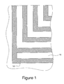
- Figure 1 is a top view of a portion of printed matter according to the present invention.
- Figure 2 is a cross section showing clear resin applied to a substrate and ink lines according to the present invention before any flow has occurred in the ink due to different surface tensions.
- Figure 3 is a cross section of printed matter according to the present invention.
- Figures 1-3 show a section of printed matter according to the present invention.
- Figures 1 and 3 show the printed matter following curing, and
- Figure 2 shows the printed matter immediately prior to curing.
- the coating which can be a resin or varnish, is combined with an additive that lowers the surface tension of the dried coating.
- an additive that lowers the surface tension of the dried coating.
- One such additive is a hydroxy-modified polyether silane manufactured and sold by BYK-Chemie.
- the additive enhanced coating 14 is formed over the substrate 10 in a pattern of substantially parallel profile lines, leaving spaces between adjacent lines of coating 14 so that the substrate remains exposed.
- the substrate is preferably a non-printed metallized film, foil, or other reflective surface.
- the pattern is then electron beam cured. Electron beam curing produces higher ridges 16 (shown in Figure 3) due to its 100% solids chemistry. EB curing also does not produce no volatile organic compounds (VOCs) or odors, as it is performed in a vacuum. Finally, EB processing allows for nearly instantaneous curing.
- VOCs volatile organic compounds
- the electron beam curable coating is cured using a suitable electron beam source.
- Suitable electron beam sources may be obtained commercially from Energy Science, Inc. of Wilmington, Massachusetts.
- the amount of energy absorbed, also known as the dose, is measured in units of MegaRads (MR or Mrad) or kiloGrays (kGy), where one Mrad is 10 kGy, one kGy being equal to 1,000 Joules per kilogram.
- the electron energy output should be within the range of 110 keV to 170 keV at a dosage of 2.5 to 5.0 MegaRads.
- the energy is within the range of 125 keV to 135 keV at a dosage of 3.0 to 4.0 MegaRads.
- an acrylate monomer When exposed to an electron beam from a suitable source, an acrylate monomer reacts with the epoxy acrylate chains to form crosslinks.
- the precursor molecules are excited directly by the ionizing electron beam. Therefore no initiator compounds are required, so no residual volatile organic compounds are present in the finished product.
- curing is substantially instantaneous and provides a cure percentage at or near one hundred percent.
- Figure 1 shows a section of substrate 10 which has been overprinted with coating 14 in a profile pattern.
- the particular printing method used to apply the coating to the substrate is not important, and those of ordinary skill in the art will recognize that a variety of printing methods are available.
- One example of a suitable printing method is the rotogravure process. Rotogravure is preferable because it produces highly accurate images, while allowing for high press and production speeds. Rotogravure cylinders engraved by a laser will yield both the production volume and continuous channels necessary to produce the desired visual effect.
- the laser engraver is capable of engraving deep continuous channels for the ink 12, as well. Mechanical engraving with a diamond stylus will only produce large cells with narrow channels of a much smaller volume.
- An ink 12 is applied over the printed coating pattern area 14.
- the coating is preferably clear when dried.
- Figure 2 shows a cross section of some printed matter immediately after the ink 12 has been applied.
- the ink 12 is in contact with both the printed dried coating 14 and the substrate 10 between lines of coating 14. Because the surface tension of the coating 14 is lower than the surface tension of the substrate 10, the ink 12 flows away from the coating 14 and toward the areas of exposed substrate 10.
- Figure 3 shows a cross section of printed matter according to the invention after the ink has completed its flow.
- the ink 12 has collected in the areas of exposed substrate 10 between the profile lines of coating 14.
- the ink 12 forms raised ridges 16 that are oriented along the patterned lines of coating 14.
- the coating is usually clear or translucent, refraction of light through the resin will cause the printed matter to change appearance when viewed from different angles.
- the coating 14 is allowed to set to form lasting raised profile ridges 16 oriented along the lines of the ink 12.
- the ink would normally flow out to a continuous film and would not yield a refraction pattern as contemplated by the raised ridges in the present invention.
- Other visual effects can be created by the use of various colored or metallic inks that may be substituted for the clear profile resin.
Abstract
Description
- The present invention relates to a method of printing and printed products. More specifically, the present invention relates to a method of printing profile ridges by applying resin to a low surface tension ink.
- In today's marketplace, products are often distinguished as much by the packaging in which they are presented as the quality of the product itself. A package which catches the eye of the consumer is therefore very desirable. To that end, increasingly colorful and creative graphics have been applied to packaging in an attempt to distinguish one package, and hence one product, from another.
- One popular graphic with visual appeal for consumers is the hologram. Holograms present a three dimensional image to the consumer. Unfortunately, holograms are expensive to produce, requiring high precision embossing equipment and tools. The capital expense required to produce holograms is high enough that holograms are often used as a security device.
Simpler embossing methods can be used at lower cost than holograms to produce a graphic with a textured or raised look and feel. Embossing can produce interesting visual effects when a clear profile is embossed over an image. The underlying image appears differently from various viewing angles due to refraction of light through the embossed profile. However, even simple embossing equipment typically requires a significant capital expenditure. - The present invention provides a printing process and a printed product in which a coating is combined with an additive that lowers the surface tension of the dried coating. The printing process comprises the steps of providing a coating with a surface lowing additive, printing the coating onto a pubstrate in a pattern, curing the coating with electron beam ("EB") processing, printing ink over the coating, and allowing the ink to dry. The ink flows away from the clear resin due to the difference in surface tension, forming patterns of raised ink.
- For the purpose of illustrating the invention, there is shown in the drawings a form which is presently preferred; it being understood, however, that this invention is not limited to the precise arrangements and instrumentalities shown.
- Figure 1 is a top view of a portion of printed matter according to the present invention.
- Figure 2 is a cross section showing clear resin applied to a substrate and ink lines according to the present invention before any flow has occurred in the ink due to different surface tensions.
- Figure 3 is a cross section of printed matter according to the present invention.
- In order to more clearly illustrate the invention, Figures 1-3 show a section of printed matter according to the present invention. Figures 1 and 3 show the printed matter following curing, and Figure 2 shows the printed matter immediately prior to curing.
- Before printing, the coating, which can be a resin or varnish, is combined with an additive that lowers the surface tension of the dried coating. One such additive is a hydroxy-modified polyether silane manufactured and sold by BYK-Chemie. The additive enhanced
coating 14 is formed over thesubstrate 10 in a pattern of substantially parallel profile lines, leaving spaces between adjacent lines ofcoating 14 so that the substrate remains exposed. The substrate is preferably a non-printed metallized film, foil, or other reflective surface. The pattern is then electron beam cured. Electron beam curing produces higher ridges 16 (shown in Figure 3) due to its 100% solids chemistry. EB curing also does not produce no volatile organic compounds (VOCs) or odors, as it is performed in a vacuum. Finally, EB processing allows for nearly instantaneous curing. - The electron beam curable coating is cured using a suitable electron beam source. Suitable electron beam sources may be obtained commercially from Energy Science, Inc. of Wilmington, Massachusetts. The amount of energy absorbed, also known as the dose, is measured in units of MegaRads (MR or Mrad) or kiloGrays (kGy), where one Mrad is 10 kGy, one kGy being equal to 1,000 Joules per kilogram. The electron energy output should be within the range of 110 keV to 170 keV at a dosage of 2.5 to 5.0 MegaRads. Preferably, the energy is within the range of 125 keV to 135 keV at a dosage of 3.0 to 4.0 MegaRads.
- When exposed to an electron beam from a suitable source, an acrylate monomer reacts with the epoxy acrylate chains to form crosslinks. The precursor molecules are excited directly by the ionizing electron beam. Therefore no initiator compounds are required, so no residual volatile organic compounds are present in the finished product. Moreover, curing is substantially instantaneous and provides a cure percentage at or near one hundred percent.
- Figure 1 shows a section of
substrate 10 which has been overprinted with coating 14 in a profile pattern. The particular printing method used to apply the coating to the substrate is not important, and those of ordinary skill in the art will recognize that a variety of printing methods are available. One example of a suitable printing method is the rotogravure process. Rotogravure is preferable because it produces highly accurate images, while allowing for high press and production speeds. Rotogravure cylinders engraved by a laser will yield both the production volume and continuous channels necessary to produce the desired visual effect. - The laser engraver is capable of engraving deep continuous channels for the
ink 12, as well. Mechanical engraving with a diamond stylus will only produce large cells with narrow channels of a much smaller volume. - An
ink 12 is applied over the printedcoating pattern area 14. The coating is preferably clear when dried. Figure 2 shows a cross section of some printed matter immediately after theink 12 has been applied. Theink 12 is in contact with both the printed driedcoating 14 and thesubstrate 10 between lines ofcoating 14. Because the surface tension of thecoating 14 is lower than the surface tension of thesubstrate 10, theink 12 flows away from thecoating 14 and toward the areas of exposedsubstrate 10. - Figure 3 shows a cross section of printed matter according to the invention after the ink has completed its flow. The
ink 12 has collected in the areas of exposedsubstrate 10 between the profile lines ofcoating 14. Thus, theink 12 forms raisedridges 16 that are oriented along the patterned lines of coating 14. Because the coating is usually clear or translucent, refraction of light through the resin will cause the printed matter to change appearance when viewed from different angles. Thecoating 14 is allowed to set to form lasting raisedprofile ridges 16 oriented along the lines of theink 12. - Without the additive in the coating, the ink would normally flow out to a continuous film and would not yield a refraction pattern as contemplated by the raised ridges in the present invention. Other visual effects can be created by the use of various colored or metallic inks that may be substituted for the clear profile resin.
- It should be understood that when producing the printed structure on press, independent registration control is possible for the individual profile stations, resulting in better overall registration. Further, by the use of a laser engraver, highly accurate patterns can be created. Also, more volume of the resin or coating can be deposited on the surface due to the large volume of cells produced on the laser engraver. This large volume is possible with the present invention substantially without the occurrence of "flow outs". A later applied viscous coating would also discourage such "flow outs."
- It is contemplated that further variations of the present invention are possible by the use of four color printing techniques and by the addition of scuff resistant protective coatings or the like.
- The present invention may be embodied in still further specific forms without departing from the spirit or essential attributes thereof and, accordingly, reference should be made to the appended claims, rather than to the foregoing specification, as indicating the scope of the invention.
Claims (19)
- A printing process comprising the steps of:a) providing a coating;b) adding a surface tension lowering additive to the coating;c) printing the coating onto a substrate in a pattern;d) curing the coating by electron beam processing;e) applying an ink over the substrate and the printed coating;f) allowing the ink to flow from the coating pattern areas to the non- pattern areas; andg) allowing the ink to dry in the form of raised profile ridges.
- The printing process of claim 1 wherein the coating is printed in a pattern of substantially parallel lines.
- The printing process of claim 2 wherein the coating pattern is printed such that non-printed areas remain between the substantially parallel lines of printed coating.
- The printing process of claim 2 wherein the ink forms raised ridges oriented along the printed coating pattern.
- The printing process of claim 1 wherein the coating is a resin.
- The printing process of claim 5 wherein the resin coating is clear.
- The printing process of claim 1 wherein the coating is a varnish.
- The printing process of claim 1 wherein the coating is a pattern of colored inks.
- The printing process of claim 1 wherein the coating is a metallic ink.
- The printing process of claim 1 wherein the substrate is a reflective surface.
- The printing process of claim 10 wherein the reflective surface is a metallized film.
- The printing process of claim 10 wherein the reflective surface is a foil.
- The printing process of claim 1 wherein the substrate is a clear film.
- A printing process as claimed in claim 17 wherein the additive is hydroxy-modified polyether silane.
- A printed product comprising:a) a substrate;b) a coating having a surface tension lowering additive, the coating printed in a pattern onto the substrate and cured using electron beam processing; andc) an ink printed over the cured coating pattern and forming a raised pattern within the non-coated areas of the substrate.
- The printed product of claim 15, wherein the coating pattern comprises substantially parallel lines.
- The printed product of claim 15 wherein the coating additive is hydroxy-modified polyether silane.
- The printed product of claim 15 wherein the substrate is a metallized film.
- The printed product of claim 15 wherein the coating is a metallic ink.
Applications Claiming Priority (2)
| Application Number | Priority Date | Filing Date | Title |
|---|---|---|---|
| US37271 | 2001-11-07 | ||
| US10/037,271 US7131380B2 (en) | 2001-11-07 | 2001-11-07 | EB pattern profile printing |
Publications (2)
| Publication Number | Publication Date |
|---|---|
| EP1310377A2 true EP1310377A2 (en) | 2003-05-14 |
| EP1310377A3 EP1310377A3 (en) | 2004-01-14 |
Family
ID=21893430
Family Applications (1)
| Application Number | Title | Priority Date | Filing Date |
|---|---|---|---|
| EP02257663A Withdrawn EP1310377A3 (en) | 2001-11-07 | 2002-11-05 | Electron beam cured raised pattern printing |
Country Status (7)
| Country | Link |
|---|---|
| US (1) | US7131380B2 (en) |
| EP (1) | EP1310377A3 (en) |
| JP (1) | JP2003182201A (en) |
| AR (1) | AR037157A1 (en) |
| BR (1) | BR0204611A (en) |
| CA (1) | CA2411239C (en) |
| MX (1) | MXPA02010929A (en) |
Cited By (2)
| Publication number | Priority date | Publication date | Assignee | Title |
|---|---|---|---|---|
| WO2007033250A1 (en) * | 2005-09-15 | 2007-03-22 | Sonoco Development, Inc. | Controlled peel force packaging with pattern-applied energy-cured coating |
| WO2011151536A1 (en) * | 2010-06-03 | 2011-12-08 | Pierre Guigan | Manufacture of embossed structures by printing processes |
Families Citing this family (13)
| Publication number | Priority date | Publication date | Assignee | Title |
|---|---|---|---|---|
| DE10146912A1 (en) * | 2001-09-24 | 2003-04-10 | Giesecke & Devrient Gmbh | Procedure for individualizing security documents and corresponding security document |
| US20050040643A1 (en) * | 2003-08-20 | 2005-02-24 | Mancuso Robert J. | Variable color print of an image |
| US7383999B2 (en) | 2004-12-28 | 2008-06-10 | Digimarc Corporation | ID document structure with pattern coating providing variable security features |
| US7639426B2 (en) * | 2007-12-05 | 2009-12-29 | Eastman Kodak Company | Micro-lens enhanced element |
| JP2009172943A (en) * | 2008-01-28 | 2009-08-06 | Toppan Printing Co Ltd | Printed matter and its manufacturing method |
| CN102555567B (en) * | 2010-12-31 | 2015-03-25 | 鸿富锦精密工业(深圳)有限公司 | Mark printing method |
| CA2850965C (en) * | 2011-10-05 | 2017-06-13 | Maax Bath Inc. | Decorative panel and method for manufacturing the same |
| US8934826B2 (en) | 2013-05-30 | 2015-01-13 | Xerox Corporation | Surface tension interference coating process for precise feature control |
| CA3130498C (en) | 2013-07-19 | 2024-01-02 | Maax Bath Inc. | Decorative panel having a digitally printed pattern and printing method therefor |
| US11299325B2 (en) | 2016-03-10 | 2022-04-12 | The Procter & Gamble Company | Packages with raised portions |
| US11299332B2 (en) | 2016-03-10 | 2022-04-12 | The Procter & Gamble Company | Packages with raised portions |
| US11261003B2 (en) * | 2016-03-10 | 2022-03-01 | The Procter & Gamble Company | Package with raised portions |
| JP2020006643A (en) * | 2018-07-11 | 2020-01-16 | 株式会社フォトクラフト社 | Printed material and printing method |
Citations (5)
| Publication number | Priority date | Publication date | Assignee | Title |
|---|---|---|---|---|
| US3504059A (en) * | 1965-10-12 | 1970-03-31 | Gen Electric | Method and apparatus for making three dimensional pictures |
| US4169907A (en) * | 1974-11-15 | 1979-10-02 | J. J. Barker Company Limited | Simulated ceramic tile |
| US4233343A (en) * | 1978-08-10 | 1980-11-11 | J. J. Barker Company Limited | Three-dimensional decorative surface |
| US4490410A (en) * | 1983-05-20 | 1984-12-25 | Showa Highpolymer Co., Ltd. | Method of affixing a decorative pattern to a stock or a molded component |
| GB2259874A (en) * | 1991-09-28 | 1993-03-31 | Waddingtons Cartons Ltd | Printed substrates having relief surfaces |
Family Cites Families (67)
| Publication number | Priority date | Publication date | Assignee | Title |
|---|---|---|---|---|
| US1509664A (en) | 1922-04-12 | 1924-09-23 | George H Brown | Color printing |
| US2793585A (en) | 1953-06-26 | 1957-05-28 | American Optical Corp | Embossing dies and method of making same |
| US3134892A (en) * | 1960-08-06 | 1964-05-26 | United Aircraft Corp | Method and apparatus for the machining of material by means of a beam of charge carriers |
| US3647959A (en) * | 1968-06-24 | 1972-03-07 | Robert J Schlesinger | System for generating a hologram |
| US3811915A (en) * | 1971-04-27 | 1974-05-21 | Inmont Corp | Printing method for forming three dimensional simulated wood grain,and product formed thereby |
| US3750117A (en) * | 1971-09-30 | 1973-07-31 | Gen Electric | Electron beam addressable archival memory |
| GB1414504A (en) | 1972-11-06 | 1975-11-19 | British American Tobacco Co | Surface finishes |
| US4124947A (en) | 1975-11-14 | 1978-11-14 | Adolf Kuhl | Graphic pattern or the like and method of producing the same |
| US4184700A (en) | 1975-11-17 | 1980-01-22 | Lgz Landis & Gyr Zug Ag | Documents embossed with optical markings representing genuineness information |
| US4079673A (en) | 1975-12-30 | 1978-03-21 | Bernstein Donald J | Raised printing on light-transmitting sheet material |
| DE2812841A1 (en) * | 1978-03-23 | 1979-09-27 | Siemens Ag | IDENTIFICATION WITH A HOLOGRAM AND PROCEDURE FOR ITS PRODUCTION |
| JPS55146785A (en) | 1979-05-04 | 1980-11-15 | Noda Plywood Mfg Co Ltd | Decorative material and preparation thereof |
| US4329409A (en) * | 1980-08-04 | 1982-05-11 | Hughes Aircraft Company | Process for fabricating stable holograms |
| US4330604A (en) * | 1980-08-04 | 1982-05-18 | Hughes Aircraft Company | Fabrication of holograms on plastic substrates |
| DE3314327C1 (en) * | 1983-04-20 | 1984-07-26 | GAO Gesellschaft für Automation und Organisation mbH, 8000 München | ID card and method of making the same |
| US4758296A (en) * | 1983-06-20 | 1988-07-19 | Mcgrew Stephen P | Method of fabricating surface relief holograms |
| EP0201323B1 (en) * | 1985-05-07 | 1994-08-17 | Dai Nippon Insatsu Kabushiki Kaisha | Article incorporating a transparent hologramm |
| US4926255A (en) * | 1986-03-10 | 1990-05-15 | Kohorn H Von | System for evaluation of response to broadcast transmissions |
| US5697844A (en) * | 1986-03-10 | 1997-12-16 | Response Reward Systems, L.C. | System and method for playing games and rewarding successful players |
| US5759101A (en) * | 1986-03-10 | 1998-06-02 | Response Reward Systems L.C. | Central and remote evaluation of responses of participatory broadcast audience with automatic crediting and couponing |
| US5508731A (en) * | 1986-03-10 | 1996-04-16 | Response Reward Systems L.C. | Generation of enlarged participatory broadcast audience |
| US4759982A (en) | 1986-12-12 | 1988-07-26 | Minnesota Mining And Manufacturing Company | Transfer graphic article with rounded and sealed edges and method for making same |
| GB8615908D0 (en) * | 1986-06-30 | 1986-08-06 | Hugle W B | Integrated circuits |
| US4970129A (en) * | 1986-12-19 | 1990-11-13 | Polaroid Corporation | Holograms |
| US4842633A (en) * | 1987-08-25 | 1989-06-27 | Matsushita Electric Industrial Co., Ltd. | Method of manufacturing molds for molding optical glass elements and diffraction gratings |
| DE3731853A1 (en) * | 1987-09-22 | 1989-03-30 | Gao Ges Automation Org | MULTI-LAYER ID CARD USED AS A PRINT AND METHOD FOR THE PRODUCTION THEREOF |
| US5019202A (en) * | 1987-12-15 | 1991-05-28 | Dai Nippon Insatsu Kabushiki Kaisha | Process for producing decorative sheets having embossed pattern |
| US5003915A (en) * | 1988-04-18 | 1991-04-02 | American Bank Note Holographics, Inc. | Apparatus for printing and for forming a hologram on sheet material |
| US4933120A (en) * | 1988-04-18 | 1990-06-12 | American Bank Note Holographics, Inc. | Combined process of printing and forming a hologram |
| JPH0243590A (en) * | 1988-08-03 | 1990-02-14 | Sharp Corp | Production of blaze hologram |
| US5058992A (en) * | 1988-09-07 | 1991-10-22 | Toppan Printing Co., Ltd. | Method for producing a display with a diffraction grating pattern and a display produced by the method |
| US4910292A (en) * | 1988-10-14 | 1990-03-20 | Eastman Kodak Company | Water-dissipatable polyester resins and coatings prepared therefrom |
| US4908063A (en) | 1988-11-04 | 1990-03-13 | Petrolite Corporation | Additive composition for water-based inks |
| US5008144A (en) | 1988-11-04 | 1991-04-16 | Petrolite Corporation | Overprint aqueous varnish |
| US4898648A (en) * | 1988-11-15 | 1990-02-06 | Pacific Bell | Method for providing a strengthened conductive circuit pattern |
| US4933218A (en) * | 1988-12-28 | 1990-06-12 | Longobardi Lawrence J | Sign with transparent substrate |
| US5085514A (en) * | 1989-08-29 | 1992-02-04 | American Bank Note Holographics, Inc. | Technique of forming a separate information bearing printed pattern on replicas of a hologram or other surface relief diffraction pattern |
| US5116548A (en) | 1989-08-29 | 1992-05-26 | American Bank Note Holographics, Inc. | Replicaton of microstructures by casting in controlled areas of a substrate |
| US5639391A (en) * | 1990-09-24 | 1997-06-17 | Dale Electronics, Inc. | Laser formed electrical component and method for making the same |
| US5633735A (en) * | 1990-11-09 | 1997-05-27 | Litel Instruments | Use of fresnel zone plates for material processing |
| US5106126A (en) * | 1990-11-29 | 1992-04-21 | Longobardi Lawrence J | Process printed image with reflective coating |
| US5742432A (en) | 1991-12-19 | 1998-04-21 | Bianco; James S. | Apparatus for manufacture of diffraction gratings for identification means |
| US5539440A (en) | 1992-03-30 | 1996-07-23 | Kabushiki Kaisha Toshiba | Image forming apparatus having colorant holding regions and a colorant repelling region |
| US5304411A (en) * | 1992-05-13 | 1994-04-19 | Borden, Inc. | Chemical embossed polyvinyl chloride film |
| US5330799A (en) | 1992-09-15 | 1994-07-19 | The Phscologram Venture, Inc. | Press polymerization of lenticular images |
| DE4243987C2 (en) * | 1992-12-23 | 2003-10-09 | Gao Ges Automation Org | ID cards with visually visible authenticity |
| EP0608458B1 (en) * | 1993-01-29 | 2002-01-02 | Citizen Watch Co. Ltd. | A method of operating an optical modulator device |
| US5538674A (en) | 1993-11-19 | 1996-07-23 | Donnelly Corporation | Method for reproducing holograms, kinoforms, diffractive optical elements and microstructures |
| US5401303A (en) | 1994-04-26 | 1995-03-28 | E. I. Du Pont De Nemours And Company | Aqueous inks having improved halo characteristics |
| JP3321596B2 (en) * | 1994-07-18 | 2002-09-03 | 凸版印刷株式会社 | Three-dimensional patterned decorative paper and method for producing the same |
| US5505320A (en) * | 1994-11-22 | 1996-04-09 | International Business Machines Corporation | Method employing laser ablating for providing a pattern on a substrate |
| US5716682A (en) * | 1995-12-06 | 1998-02-10 | S & G Chromium Graphics | Three dimensional card |
| GB9524862D0 (en) * | 1995-12-06 | 1996-02-07 | The Technology Partnership Plc | Colour diffractive structure |
| US5838468A (en) * | 1996-04-12 | 1998-11-17 | Nec Corporation | Method and system for forming fine patterns using hologram |
| EP2254003A3 (en) * | 1996-09-19 | 2011-11-16 | Dai Nippon Printing Co., Ltd. | Multilayered volume hologram structure, and label for making multilayered volume hologram structure |
| CA2200675C (en) * | 1997-03-21 | 2003-12-23 | Chen Wu | A printed antenna structure for wireless data communications |
| US5982545A (en) * | 1997-10-17 | 1999-11-09 | Industrial Technology Research Institute | Structure and method for manufacturing surface relief diffractive optical elements |
| US5968607A (en) * | 1997-12-10 | 1999-10-19 | Chromium Graphics | Device and method for etch and emboss process printing |
| US6222157B1 (en) * | 1998-04-17 | 2001-04-24 | L.A. Batchelder And Sons Consulting, Inc. | Seamless holographic transfer using laser generated optical effect patterns |
| WO1999055530A1 (en) * | 1998-04-24 | 1999-11-04 | Fargo Electronics, Inc. | Refractive overlaminate panel technique for the production of identification cards |
| US6087416A (en) | 1998-07-22 | 2000-07-11 | E.I. Du Pont De Nemours And Company | Aqueous pigmented ink jet inks for printing on vinyls |
| US6439708B1 (en) | 1998-07-27 | 2002-08-27 | Seiko Epson Corporation | Method of ink-jet recording with two fluids |
| US6087940A (en) * | 1998-07-28 | 2000-07-11 | Novavision, Inc. | Article surveillance device and method for forming |
| ATE260181T1 (en) | 1998-12-18 | 2004-03-15 | Avecia Ltd | INKJET PRINTING PROCESS USING POLYMER BIGUANIDES |
| US6147662A (en) * | 1999-09-10 | 2000-11-14 | Moore North America, Inc. | Radio frequency identification tags and labels |
| US6551694B1 (en) * | 1999-11-12 | 2003-04-22 | Toppan Printing Co., Ltd. | Thermosetting resin decorative board and method of producing the same |
| US6546872B1 (en) * | 2000-11-27 | 2003-04-15 | Sonoco Development, Inc. | Profile printing method with additive technology |
-
2001
- 2001-11-07 US US10/037,271 patent/US7131380B2/en not_active Expired - Fee Related
-
2002
- 2002-10-30 AR ARP020104125A patent/AR037157A1/en unknown
- 2002-11-04 BR BR0204611-3A patent/BR0204611A/en not_active Application Discontinuation
- 2002-11-05 EP EP02257663A patent/EP1310377A3/en not_active Withdrawn
- 2002-11-06 MX MXPA02010929A patent/MXPA02010929A/en active IP Right Grant
- 2002-11-06 CA CA2411239A patent/CA2411239C/en not_active Expired - Fee Related
- 2002-11-06 JP JP2002322528A patent/JP2003182201A/en not_active Withdrawn
Patent Citations (5)
| Publication number | Priority date | Publication date | Assignee | Title |
|---|---|---|---|---|
| US3504059A (en) * | 1965-10-12 | 1970-03-31 | Gen Electric | Method and apparatus for making three dimensional pictures |
| US4169907A (en) * | 1974-11-15 | 1979-10-02 | J. J. Barker Company Limited | Simulated ceramic tile |
| US4233343A (en) * | 1978-08-10 | 1980-11-11 | J. J. Barker Company Limited | Three-dimensional decorative surface |
| US4490410A (en) * | 1983-05-20 | 1984-12-25 | Showa Highpolymer Co., Ltd. | Method of affixing a decorative pattern to a stock or a molded component |
| GB2259874A (en) * | 1991-09-28 | 1993-03-31 | Waddingtons Cartons Ltd | Printed substrates having relief surfaces |
Cited By (4)
| Publication number | Priority date | Publication date | Assignee | Title |
|---|---|---|---|---|
| WO2007033250A1 (en) * | 2005-09-15 | 2007-03-22 | Sonoco Development, Inc. | Controlled peel force packaging with pattern-applied energy-cured coating |
| WO2011151536A1 (en) * | 2010-06-03 | 2011-12-08 | Pierre Guigan | Manufacture of embossed structures by printing processes |
| FR2960820A1 (en) * | 2010-06-03 | 2011-12-09 | Pierre Guigan | FABRICATION OF STRUCTURES IN RELIEF BY PRINTING PROCESSES |
| US9242270B2 (en) | 2010-06-03 | 2016-01-26 | Pierre Guigan | Manufacture of embossed structures by printing processes |
Also Published As
| Publication number | Publication date |
|---|---|
| JP2003182201A (en) | 2003-07-03 |
| MXPA02010929A (en) | 2004-07-16 |
| CA2411239A1 (en) | 2003-05-07 |
| EP1310377A3 (en) | 2004-01-14 |
| CA2411239C (en) | 2010-08-10 |
| US20030087072A1 (en) | 2003-05-08 |
| US7131380B2 (en) | 2006-11-07 |
| AR037157A1 (en) | 2004-10-27 |
| BR0204611A (en) | 2003-09-16 |
Similar Documents
| Publication | Publication Date | Title |
|---|---|---|
| US6546872B1 (en) | Profile printing method with additive technology | |
| US7131380B2 (en) | EB pattern profile printing | |
| CA2536533C (en) | Engraved optically variable image device | |
| RU2590880C2 (en) | Method of forming three-dimensional images in coatings | |
| EP3526043B1 (en) | Method for generating a superficial structure | |
| FI122671B (en) | Method of manufacturing a visually identifiable pattern on a substrate | |
| CN1272753C (en) | Method for producing a laser-printable film | |
| RU2350997C2 (en) | Composition and method of making colour hologram | |
| EP1685974B1 (en) | Security marking and manufacturing process therefor | |
| JPH11320804A (en) | Decorative sheet with tuned emboss and manufacture thereof | |
| JP6293130B2 (en) | How to create a three-dimensional pattern on a liquid crystal coating | |
| JPS5814312B2 (en) | Decorative sheet and its manufacturing method | |
| CN111892858A (en) | Lithographic offset printing ink fountain UV gloss oil capable of realizing local laser transfer and lithographic offset printing method | |
| JP6914954B2 (en) | A method of printing a substrate with a printing substance containing a metal pigment, and a substrate printed with a printing substance containing metal particles. | |
| KR101397348B1 (en) | The intaglio printing paper coated side effects of treatment manufacturing methods and matte etched pattern imprint | |
| JPH0257345A (en) | Embossed pattern forming method by printing | |
| US20210107274A1 (en) | An apparatus and process for printing with tactile and glitter effect on flexible substrate and printed substrate thereof | |
| JPS631577A (en) | Production of natural wood tone facing capable of freely being colored | |
| JPH0477254A (en) | Formation of uneven pattern | |
| ITUD20070229A1 (en) | PROCEDURE AND RELATIVE EQUIPMENT TO REALIZE A PANEL AND PANEL SO REALIZABLE |
Legal Events
| Date | Code | Title | Description |
|---|---|---|---|
| PUAI | Public reference made under article 153(3) epc to a published international application that has entered the european phase |
Free format text: ORIGINAL CODE: 0009012 |
|
| AK | Designated contracting states |
Designated state(s): AT BE BG CH CY CZ DE DK EE ES FI FR GB GR IE IT LI LU MC NL PT SE SK TR |
|
| AX | Request for extension of the european patent |
Extension state: AL LT LV MK RO SI |
|
| PUAL | Search report despatched |
Free format text: ORIGINAL CODE: 0009013 |
|
| AK | Designated contracting states |
Kind code of ref document: A3 Designated state(s): AT BE BG CH CY CZ DE DK EE ES FI FR GB GR IE IT LI LU MC NL PT SE SK TR |
|
| AX | Request for extension of the european patent |
Extension state: AL LT LV MK RO SI |
|
| 17P | Request for examination filed |
Effective date: 20040213 |
|
| 17Q | First examination report despatched |
Effective date: 20040406 |
|
| AKX | Designation fees paid |
Designated state(s): DE FR GB IT |
|
| STAA | Information on the status of an ep patent application or granted ep patent |
Free format text: STATUS: THE APPLICATION IS DEEMED TO BE WITHDRAWN |
|
| 18D | Application deemed to be withdrawn |
Effective date: 20060601 |