EP1317399B1 - Microelectromechanical flexible membrane electrostatic valve device and related fabrication methods - Google Patents
Microelectromechanical flexible membrane electrostatic valve device and related fabrication methods Download PDFInfo
- Publication number
- EP1317399B1 EP1317399B1 EP01970902A EP01970902A EP1317399B1 EP 1317399 B1 EP1317399 B1 EP 1317399B1 EP 01970902 A EP01970902 A EP 01970902A EP 01970902 A EP01970902 A EP 01970902A EP 1317399 B1 EP1317399 B1 EP 1317399B1
- Authority
- EP
- European Patent Office
- Prior art keywords
- substrate
- valve
- electrode
- dielectric layer
- mems
- Prior art date
- Legal status (The legal status is an assumption and is not a legal conclusion. Google has not performed a legal analysis and makes no representation as to the accuracy of the status listed.)
- Expired - Lifetime
Links
Images


Classifications
-
- F—MECHANICAL ENGINEERING; LIGHTING; HEATING; WEAPONS; BLASTING
- F16—ENGINEERING ELEMENTS AND UNITS; GENERAL MEASURES FOR PRODUCING AND MAINTAINING EFFECTIVE FUNCTIONING OF MACHINES OR INSTALLATIONS; THERMAL INSULATION IN GENERAL
- F16K—VALVES; TAPS; COCKS; ACTUATING-FLOATS; DEVICES FOR VENTING OR AERATING
- F16K99/00—Subject matter not provided for in other groups of this subclass
- F16K99/0001—Microvalves
-
- B—PERFORMING OPERATIONS; TRANSPORTING
- B81—MICROSTRUCTURAL TECHNOLOGY
- B81B—MICROSTRUCTURAL DEVICES OR SYSTEMS, e.g. MICROMECHANICAL DEVICES
- B81B3/00—Devices comprising flexible or deformable elements, e.g. comprising elastic tongues or membranes
- B81B3/0018—Structures acting upon the moving or flexible element for transforming energy into mechanical movement or vice versa, i.e. actuators, sensors, generators
- B81B3/0021—Transducers for transforming electrical into mechanical energy or vice versa
-
- F—MECHANICAL ENGINEERING; LIGHTING; HEATING; WEAPONS; BLASTING
- F15—FLUID-PRESSURE ACTUATORS; HYDRAULICS OR PNEUMATICS IN GENERAL
- F15C—FLUID-CIRCUIT ELEMENTS PREDOMINANTLY USED FOR COMPUTING OR CONTROL PURPOSES
- F15C5/00—Manufacture of fluid circuit elements; Manufacture of assemblages of such elements integrated circuits
-
- F—MECHANICAL ENGINEERING; LIGHTING; HEATING; WEAPONS; BLASTING
- F16—ENGINEERING ELEMENTS AND UNITS; GENERAL MEASURES FOR PRODUCING AND MAINTAINING EFFECTIVE FUNCTIONING OF MACHINES OR INSTALLATIONS; THERMAL INSULATION IN GENERAL
- F16K—VALVES; TAPS; COCKS; ACTUATING-FLOATS; DEVICES FOR VENTING OR AERATING
- F16K99/00—Subject matter not provided for in other groups of this subclass
- F16K99/0001—Microvalves
- F16K99/0003—Constructional types of microvalves; Details of the cutting-off member
- F16K99/0005—Lift valves
- F16K99/0007—Lift valves of cantilever type
-
- F—MECHANICAL ENGINEERING; LIGHTING; HEATING; WEAPONS; BLASTING
- F16—ENGINEERING ELEMENTS AND UNITS; GENERAL MEASURES FOR PRODUCING AND MAINTAINING EFFECTIVE FUNCTIONING OF MACHINES OR INSTALLATIONS; THERMAL INSULATION IN GENERAL
- F16K—VALVES; TAPS; COCKS; ACTUATING-FLOATS; DEVICES FOR VENTING OR AERATING
- F16K99/00—Subject matter not provided for in other groups of this subclass
- F16K99/0001—Microvalves
- F16K99/0003—Constructional types of microvalves; Details of the cutting-off member
- F16K99/0028—Valves having multiple inlets or outlets
-
- F—MECHANICAL ENGINEERING; LIGHTING; HEATING; WEAPONS; BLASTING
- F16—ENGINEERING ELEMENTS AND UNITS; GENERAL MEASURES FOR PRODUCING AND MAINTAINING EFFECTIVE FUNCTIONING OF MACHINES OR INSTALLATIONS; THERMAL INSULATION IN GENERAL
- F16K—VALVES; TAPS; COCKS; ACTUATING-FLOATS; DEVICES FOR VENTING OR AERATING
- F16K99/00—Subject matter not provided for in other groups of this subclass
- F16K99/0001—Microvalves
- F16K99/0034—Operating means specially adapted for microvalves
- F16K99/0042—Electric operating means therefor
- F16K99/0051—Electric operating means therefor using electrostatic means
-
- B—PERFORMING OPERATIONS; TRANSPORTING
- B81—MICROSTRUCTURAL TECHNOLOGY
- B81B—MICROSTRUCTURAL DEVICES OR SYSTEMS, e.g. MICROMECHANICAL DEVICES
- B81B2201/00—Specific applications of microelectromechanical systems
- B81B2201/05—Microfluidics
- B81B2201/054—Microvalves
-
- B—PERFORMING OPERATIONS; TRANSPORTING
- B81—MICROSTRUCTURAL TECHNOLOGY
- B81B—MICROSTRUCTURAL DEVICES OR SYSTEMS, e.g. MICROMECHANICAL DEVICES
- B81B2203/00—Basic microelectromechanical structures
- B81B2203/01—Suspended structures, i.e. structures allowing a movement
- B81B2203/0127—Diaphragms, i.e. structures separating two media that can control the passage from one medium to another; Membranes, i.e. diaphragms with filtering function
-
- B—PERFORMING OPERATIONS; TRANSPORTING
- B81—MICROSTRUCTURAL TECHNOLOGY
- B81B—MICROSTRUCTURAL DEVICES OR SYSTEMS, e.g. MICROMECHANICAL DEVICES
- B81B2203/00—Basic microelectromechanical structures
- B81B2203/04—Electrodes
-
- F—MECHANICAL ENGINEERING; LIGHTING; HEATING; WEAPONS; BLASTING
- F16—ENGINEERING ELEMENTS AND UNITS; GENERAL MEASURES FOR PRODUCING AND MAINTAINING EFFECTIVE FUNCTIONING OF MACHINES OR INSTALLATIONS; THERMAL INSULATION IN GENERAL
- F16K—VALVES; TAPS; COCKS; ACTUATING-FLOATS; DEVICES FOR VENTING OR AERATING
- F16K99/00—Subject matter not provided for in other groups of this subclass
- F16K2099/0073—Fabrication methods specifically adapted for microvalves
- F16K2099/0074—Fabrication methods specifically adapted for microvalves using photolithography, e.g. etching
-
- F—MECHANICAL ENGINEERING; LIGHTING; HEATING; WEAPONS; BLASTING
- F16—ENGINEERING ELEMENTS AND UNITS; GENERAL MEASURES FOR PRODUCING AND MAINTAINING EFFECTIVE FUNCTIONING OF MACHINES OR INSTALLATIONS; THERMAL INSULATION IN GENERAL
- F16K—VALVES; TAPS; COCKS; ACTUATING-FLOATS; DEVICES FOR VENTING OR AERATING
- F16K99/00—Subject matter not provided for in other groups of this subclass
- F16K2099/0073—Fabrication methods specifically adapted for microvalves
- F16K2099/008—Multi-layer fabrications
-
- H—ELECTRICITY
- H01—ELECTRIC ELEMENTS
- H01H—ELECTRIC SWITCHES; RELAYS; SELECTORS; EMERGENCY PROTECTIVE DEVICES
- H01H59/00—Electrostatic relays; Electro-adhesion relays
- H01H59/0009—Electrostatic relays; Electro-adhesion relays making use of micromechanics
- H01H2059/0081—Electrostatic relays; Electro-adhesion relays making use of micromechanics with a tapered air-gap between fixed and movable electrodes
Definitions
- the present invention relates to microelectromechanical system (MEMS) valve structures, and more particularly to low-power, high speed electrostatically actuating MEMS valve structures and the associated fabrication methods.
- MEMS microelectromechanical system
- MEMS Micro Electro Mechanical System
- MEMS structures are typically capable of motion or applying force.
- Many different varieties of MEMS devices have been created, including microsensors, microgears, micromotors, and other microengineered devices. MEMS devices are being developed for a wide variety of applications because they provide the advantages of low cost, high reliability and extremely small size.
- microcantilevers have been used to apply rotational mechanical force to rotate micromachined springs and gears.
- Electromagnetic fields have been used to drive micromotors.
- Piezoelectric forces have also been successfully been used to controllably move micromachined structures.
- Controlled thermal expansion of actuators or other MEMS components has been used to create forces for driving microdevices.
- One such device is found in United States Patent No. 5,475,318 entitled “Microprobe” issued December 12, 1995 in the name of inventors Marcus et al., which leverages thermal expansion to move a microdevice.
- a micro cantilever is constructed from materials having different thermal coefficients of expansion. When heated, the bimorph layers arch differently, causing the micro cantilever to move accordingly.
- a similar mechanism is used to activate a micromachined thermal switch as described in United States Patent No. 5,463,233 entitled “Micromachined Thermal Switch” issued October 31, 1995 in the name of inventor Norling.
- Electrostatic forces have also been used to move structures.
- Traditional electrostatic devices were constructed from laminated films cut from plastic or mylar materials. A flexible electrode was attached to the film, and another electrode was affixed to a base structure. Electrically energizing the respective electrodes created an electrostatic force attracting the electrodes to each other or repelling them from each other.
- a representative example of these devices is found in United States Patent No. 4,266,339 entitled “Method for Making Rolling Electrode for Electrostatic Device” issued May 12, 1981 in the name of inventor Kalt. These devices work well for typical motive applications, but these devices cannot be constructed in dimensions suitable for miniaturized integrated circuits, biomedical applications, or MEMS structures.
- MEMS electrostatic devices are used advantageously in various applications because of their extremely small size. Electrostatic forces due to the electric field between electrical charges can generate relatively large forces given the small electrode separations inherent in MEMS devices.
- An example of these devices can be found in United States Patent Application No. 09/345,300 entitled “ARC resistant High Voltage Micromachined Electrostatic Switch” filed on June 30, 1999 in the name of inventor Goodwin-Johansson and Untied States Patent Application No. 09/320,891 entitled “Micromachined Electrostatic Actuator with Air Gap” filed on May 27, 1999 in the name of inventor Goodwin-Johansson. Both of these applications are assigned to MCNC, the assignee of the present invention.
- Typical MEMS valves have employed thermal actuation/activation methods to control valves with high flow rates (i.e. large apertures and large clearance areas around the aperture). Thermal actuation has been preferred because it is able to provide the large forces necessary to control the valve over the requisite large distances. However, these valves have relatively slow operation rates due to the thermal time constraints related to the valve materials. Additionally, thermally activated MEMS valves use resistive heating where the power consumed is calculated by the current squared times the resistance and considerable power is consumed in operating the valve.
- US 5,441,597 discloses a process for fabricating a flow control device which includes a flexible membrane forming a partition between a main flow passage and a control chamber.
- US 5,771,902 discloses devices for navigation of endovascular guidewires and/or catheters including micromachined cantilevered actuators, rudders, microvalves, force sensors and positioning or steering mechanisms.
- MEMS valve device using electrostatic actuation that is capable of both large displacements and large forces.
- the electrostatic nature of the MEMS valve will allow for relatively low power consumption and, therefore, no unwarranted heating of the flowing gas or fluid would occur. Additionally, the electrostatic valve will provide for relatively fast operation, allowing for more precise control of the open and closed states of the valve.
- Stiction which is a well-known concept in microelectronics, is defined as the tendency for contacting MEMS surfaces to stick to one another. Stiction is especially a concern in valve devices in which a pressure differential exists across the closed valve. It would be beneficial to devise a MEMS valve that relieves the pressure differential prior to opening the valve.
- MEMS electrostatic valves that have improved performance characteristics are desired for many applications.
- micromachined valves capable of fast actuation, large valve force and large valve flap displacements that utilize minimal power are desirable, but are currently unavailable.
- the present invention provides for improved MEMS electrostatic valves that benefit from large valve force, fast actuation and large displacement of the moveable membrane to allow for the efficient transport of increased amounts of gas or liquid through the valve. Further, methods for making the MEMS electrostatic valve according to the present invention are provided.
- a MEMS valve device driven by electrostatic forces is provided as claimed in claim 1.
- the resiliently compressible dielectric layer is formed on the substrate electrode and provides for the valve seat surface.
- the resiliently compressible dielectric layer is formed on the moveable membrane and provides for the valve seal surface.
- resiliently compressible dielectric layers are formed on both the substrate electrode and the moveable membrane and provide for both the valve seat surface and the valve seal surface. The resiliently compressible nature of the dielectric layer allows for a secure closed valve to form that benefits from a low leakage rate.
- the resiliently compressible dielectric layer has a textured surface; either at the valve seat, the valve seal or at both surfaces.
- a textured surface By texturing these surfaces the valve is able to overcome stiction that causes the MEMS films to stick together after the electrostatic voltage is removed. In effect, texturing reduces the surface area around the valve seat to seal interface thereby reducing the effects of stiction. Additionally, texturing allows pressure to be advantageously used in easing the opening of the valve.
- a pressure-relieving aperture is defined within the planar substrate and is positioned to underlie the moveable membrane.
- the pressure-relieving aperture provides a decrease in the pressure differential across the valve aperture by alleviating pressure prior to the opening of the valve.
- another embodiment of the present invention provides for a MEMS valve array driven by electrostatic forces as claimed in claim 20.
- the array configuration allows for increased gas or liquid flows.
- the substrate has a plurality of apertures and a plurality of substrate electrodes is provided; wherein each aperture has a corresponding substrate electrode.
- the substrate electrodes can be individually supplied electrostatic voltages, thus controlling the number of apertures opened or closed. This configuration effectuates a variable flow rate valve.
- the array of the present invention is embodied in a substrate having a plurality of apertures and a shaped electrode element within the moveable membrane and/or the substrate.
- the shaped nature of the electrode element allows for the amount of membrane uncurling to be adjusted in accordance with the amount of voltage applied between the electrodes.
- An example provides a method for making the MEMS valve device described above.
- the method comprises the steps of etching the frontside of a substrate to define an aperture extending partially through the substrate, filling the aperture with a plug material, forming a membrane valve structure on the frontside of the substrate, removing the plug material, etching the backside of the valve aperture up to the release layer and removing the release layer to at least partially release the membrane from the substrate.
- the method provided allows for the alignment of the aperture and the substrate electrode to be accomplished on the frontside of the substrate.
- the MEMS valve device driven by electrostatic force is capable of both large displacements and large forces.
- the electrostatic nature of the MEMS valve allows for relatively low power consumption and, therefore, no unwarranted heating of the flowing gas or fluid occurs.
- the electrostatic valve will provide for relatively fast operation, allowing for faster cycle time and more precise control of the open and closed states.
- the MEMS valve provides for a secure valve seat to valve cover interface to assure low leakage rates.
- An additional benefit is realized in providing for a MEMS valve that minimizes the occurrence of stiction between the substrate and moveable membrane. Stiction is overcome by providing for textured surfaces at the valve seat and/or valve seal interface or allowing for a pressure-relieving aperture to be defined in the substrate.
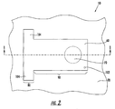
- an electrostatic MEMS valve device comprises in layers, a generally planar substrate 20 , a substrate insulator 30 , a substrate electrode 40 , a substrate dielectric 50 , and a moveable membrane 60 .
- the substrate defines an aperture 70 formed therethrough that serves as the valve opening,
- the aperture is formed in cooperation with the substrate, the substrate insulator, the substrate electrode and the substrate dielectric.
- the aperture may be formed through the substrate, the substrate insulator, the substrate electrode and/or the substrate dielectric.
- the aperture will be cylindrical in shape.
- other shapes such as, a funnel shape having a smaller perimeter at the valve seat and a larger perimeter at the backside opening of the substrate, are also possible and within the breadth of the invention disclosed.
- the movable membrane may be described as having two portions referred to as the fixed portion 80 and the distal portion 90 .
- the portions are deposited horizontally along the length of the moveable membrane.
- the fixed portion is substantially affixed to the underlying substrate or intermediate layers at the attachment point 100 .
- the distal portion is released from the underlying substrate or intermediate layers during fabrication of the MEMS valve device.
- the distal portion of the device is moveable with respect to the underlying substrate and substrate electrode. The movement of the distal portion thereby controllably adjusts the portion of the aperture covered by the moveable membrane.
- the moveable membrane 60 comprises multiple layers including at least one electrode element layer 62 and at least one biasing element layer 64 and/or 66 .
- the biasing element(s) provide the moveable membrane with the biased shape shown in FIG.1 . Once the moveable membrane is released from the substrate during fabrication, the biasing element allows the overall membrane structure to position itself distant from the substrate. In the embodiment shown in FIG. 1 biasing provides for the upward curled shape of the moveable membrane. Biasing can be accomplished by providing for materials of dissimilar coefficients of thermal expansion, materials having substantive differences in cross-sectional thickness or other material characteristics may also effect biasing.
- the electrode element provides the moveable membrane with a means for electrostatic actuation. In valve operation a voltage is supplied to the electrode element and it is electrostatically attracted toward the substrate electrode. As the electrode element comes in contact with the substrate construct, the moveable membrane forms a valve seal that serves to seal-off the aperture formed in the substrate.
- the electrostatic MEMS valve device including the moveable membrane and underlying substrate layers, is constructed using known integrated circuit materials and microengineering techniques. Those skilled in the art will understand that different materials, various numbers of layers, and numerous arrangements of layers may also be used to form the underlying substrate layers and the moveable membrane. Although the MEMS valve device illustrated in the figures will be used as an example to describe manufacturing details, this discussion applies equally to all MEMS valve devices provided by the present invention unless otherwise noted.
- a substrate 20 defines a generally planar surface 22 upon which the electrostatic MEMS valve device is constructed.
- the substrate comprises a microelectronic substrate, such as silicon, although any suitable substrate material having a generally planar surface can be used.
- the further processing steps involved in the fabrication of the present invention may be performed at relatively low temperatures and, therefore, the substrate that is used is not limited to conventional higher temperature substrates.
- quartz, glass, or other suitable materials having insulating tendencies may serve as the substrate.
- a substrate insulator layer 30 typically overlies the planar surface of the substrate and provides electrical isolation. In certain embodiments that implement substrate materials having strong insulation characteristics it may be possible to form the MEMS valve device without the substrate insulator layer.
- the substrate insulator layer preferably comprises a non-oxidation-based insulator or polymer, such as polyimide or nitride.
- oxide based insulators are avoided if certain acids (such as hydrofluoric acid) are used in processing to remove the release layer.
- the substrate insulator layer is preferably formed by using a standard deposition technique, such as conventional spinning or low-pressure chemical vapor deposition (LPCVD), to deposit the insulating layer on the planar surface of the substrate.
- LPCVD low-pressure chemical vapor deposition
- a substrate electrode 40 is deposited as a generally planar layer affixed to at least a portion of the surface of the underlying substrate insulator layer 30 or substrate 20 .
- the substrate electrode preferably comprises a gold layer deposited on the top surface of the insulator layer. If the substrate electrode is formed from a layer of gold, optionally a thin layer of chromium may be deposited prior to depositing the substrate signal electrode layer to allow better adhesion to the insulating layer and/or after the substrate signal electrode layer has been deposited to allow better adhesion to any subsequent adjacent materials. Alternatively, other suitable metallic or conductive materials may be used for the substrate signal electrode so long as release layer processing operations does not result in electrode erosion. Standard photolithography and etching techniques are typically used to deposit the electrode on the surface of the substrate.
- a substrate dielectric layer 50 is deposited on the substrate electrode to provide for a dielectric that electrically isolates the substrate signal from the electrode element found in the moveable membrane.
- this layer serves as the valve seat 52 that surrounds the valve aperture.
- the substrate dielectric layer will comprise a resiliently compressible material. Resiliency for any given material can be assessed by comparing (a) the ratio of the electrostatic force of the valve around the aperture to the valve seat area (i.e. the applied pressure) versus (b) the product of Young's modulus (measure of elasticity) for the given material and the ratio of the surface roughness of the valve seat to the thickness of the valve seat.
- the resiliently compressible nature of the substrate dielectric layer will allow for the valve seat to deform upon contact with the moveable membrane.
- the deforming characteristic of the valve seat provides for a sound valve seal to form, thus providing for improved off-flow.
- One such resiliently compressable substrate dielectric material comprises polyimide, although other resiliently compressible dielectric insulators or polymers tolerant of release layer processing may also be used.
- the substrate dielectric layer is formed using a conventional deposition technique, such as standard spinning techniques or low-pressure chemical vapor deposition LPCVD.
- the substrate dielectric layer 50 may be formed with a generally planar surface (as shown in FIG.1 ) or the substrate dielectric layer may be formed with a textured surface.
- a textured surface at the valve seat 52 area may be preferred in those embodiments in which the moveable membrane "sticks" to the underlying substrate when release is desired.
- the MEMS phenomena related to the tendency of two mating MEMS surfaces to stick together is known in the art as stiction.
- stiction By providing for a textured surface at the valve seat less surface area is contacting the moveable membrane when the valve seal is closed and thus less force is necessary to overcome the stiction. Textured surfaces are typically formed during fabrication and the implementation and fabrication of such surfaces is well known in the art.
- a release layer (not shown in FIGS. 1 and 2 ), is deposited on the surface of the substrate dielectric layer 50 in the area generally underneath the distal portion of the overlying moveable membrane.
- the release layer is only deposited on those regions below moveable membrane portions not being affixed to the underlying substrate structure.
- the release layer comprises an oxide or other suitable material that may be etched away when acid is applied thereto.
- the release layer may be removed through standard microengineering acidic etching techniques, such as a hydrofluoric acid etch. When the release layer has been removed, the distal portion 90 of moveable membrane 60 is separated from the underlying surface.
- the release of the moveable membrane from the substrate in conjunction with the biasing characteristics of the biasing element will typically result in the thin film membrane having a distal portion that has a curled shape. Biasing in the moveable membrane will typically result in the moveable membrane curling away from the substrate (as shown in FIG.1 ) when no electrostatic force is applied. It is also possible to bias the moveable membrane such that it curls toward the substrate when no electrostatic force is applied.
- Biasing in the moveable membrane may be accomplished by providing for biasing element and electrode element materials that differ in thickness, thermal coefficient of expansion or any other known biasing characteristic. Alternately, biasing may be induced during fabrication by employing process steps that create intrinsic stresses so as to curl the moveable membrane.
- a polymeric biasing element can be deposited as a liquid and then cured by elevated temperatures so that it forms a solid biasing layer.
- the biasing element may comprise a polymer material having a higher thermal coefficient of expansion than the electrode element. Next, the biasing element and the electrode element are cooled, inducing stresses in the membrane due to differences in the thermal coefficients of expansion. The moveable membrane curls because the polymeric biasing element shrinks faster than the electrode layer.
- providing differential thermal coefficients of expansion between the biasing element layers and the electrode element layer can create bias. Assuming an increase in temperature, the moveable membrane will curl toward the layer having the lower thermal coefficient of expansion because the layers accordingly expand at different rates. As such, the moveable membrane having two layers with different thermal coefficients of expansion will curl toward the layer having a lower thermal coefficient of expansion as the temperature rises.
- two polymer film layers having different thermal coefficients of expansion can be used in tandem with an electrode layer to bias the moveable membrane as necessary.
- the layers of the moveable membrane 60 generally overlie the substrate electrode 40 and the aperture 70 .
- Known integrated circuit manufacturing processes are used to construct the layers comprising moveable membrane 60 .
- the moveable membrane is comprised of an electrode element and a biasing element.
- one or more layers of the moveable membrane comprise the electrode element and one or more additional layers comprise the biasing element.
- one preferred embodiment of the moveable membrane comprises an electrode element layer 62 positioned between two biasing element layers 64 and 66 . It is also possible to configure the moveable membrane with an electrode element layer having only one biasing layer positioned on either side of the electrode element layer.
- the biasing element layer may also serve as an insulator that allows for the complete electrical isolation between the substrate electrode and the electrode element of the moveable membrane.
- the layers comprising the moveable membrane is formed from a flexible material, for instance flexible polymers (i.e: the biasing element) and/or flexible conductors (i.e. the electrodes) may be used.
- the biasing element will comprise a flexible polymer film used to hold the moveable membrane in a stationary position absent electrostatic forces.
- the biasing element contacts the substrate to form the valve seal the biasing element comprises a resiliently compressible material.
- the resiliently compressible nature of the biasing element layer will allow for the valve seal to deform upon contact with the underlying substrate structure.
- the deforming characteristic of the contacting biasing element surface provides for a sound valve seal to form, thus providing for improved off-flow.
- a polymer film material that has resiliently compressible characteristics may include a polyimide material, however, other suitable flexible polymers having resilient characteristics and capable of withstanding the release layer etch process can also be employed.
- both the substrate dielectric layer and the biasing element layer of the moveable membrane are formed of a resiliently compressible material, such as a polyimide material.
- the electrode element 62 of the moveable membrane 60 preferably comprises a layer of flexible conductor material.
- the electrode element may be deposited directly upon the uppermost planar surface of the substrate construct and the release layer or over an optional first biasing layer (i.e. polymer film), as needed.
- the electrode element preferably comprises gold, although other conductors tolerant of release layer processing and other flexible materials, such as conductive polymer film, may be used.
- the surface area and/or configuration of the electrode element can be varied as required to allow for the desired electrostatic forces to operate the MEMS valve device. By shaping the electrode element in a predetermined fashion it is possible to effectuate changes in the valve release rate. If gold is used to form the electrode element, a thin layer of chromium may be deposited onto the electrode element to allow better adhesion of the gold layer to the adjacent materials, such as to one or more biasing layers of flexible polymer film or the like.
- the number of layers, thickness of layers, arrangement of layers, and choice of materials used in the moveable membrane may be selected to bias the moveable membrane as required.
- the distal portion can be varyingly biased as it extends from the fixed portion.
- the biased position of the distal portion can be customized individually or collectively to provide a desired separation from the underlying planar surface and the substrate electrode.
- the distal portion can be biased to remain parallel to the underlying planar surface.
- the distal portion can be biased to alter the separation from the underlying planar surface by curling toward or curling away from the underlying planar surface.
- the distal portion biased to curl away from the underlying substrate and alter the separation therefrom.
- more than one polymer film layer may be used, and that the films may be deposited on either side or both sides of the electrode elements.
- the valve can be configured so that a pressure difference can be applied in either direction across the membrane when the membrane seals the aperture. If the pressure is coming from the backside of the substrate and pushing up against the membrane when the valve is closed, then the pressure will assist in the re-curling of the film when the voltage is removed. If, however, the pressure is coming from the frontside of the substrate and pushing down against the membrane when it is closed, the stress in the membrane will have to work against the applied pressure to open the valve. This pressure build-up can be minimized by providing for a small aperture through the substrate proximate the end of the distal portion of the moveable membrane.
- the curling stress can be increased in comparison to the pressure exerted at the small pressure-relieving aperture by providing for this small aperture. Once the small pressure-relieving aperture has been opened, the pressure differential across the membrane at the valve aperture will be reduced, making it easier for the stress in the membrane to open the valve.
- An example of such a pressure-relieving aperture 102 is shown in FIGS. 1 and 2 .
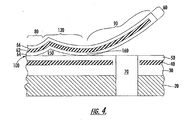
- FIG. 3 illustrates a cross-sectional view of an alternative embodiment of the MEMS electrostatic valve in accordance with the present invention.
- the MEMS electrostatic valve 10 of this embodiment has a characteristically uniform air gap 110 underlying a medial portion 120 of the moveable membrane 60 .
- the medial portion of the moveable membrane is defined as the horizontal region between the fixed portion 80 and the distal portion 90 .
- a release layer (not shown in FIG. 3 ) is deposited on the uppermost layer of the substrate construct in the area underlying the medial and distal portions of the moveable membrane. The release layer is subsequently removed and results in the overall spatial separation between the medial and distal portions of the membrane and the underlying substrate.
- the medial portion is constructed generally similar in make-up to the distal portion and, therefore, the differential in thermal coefficients of expansion between the electrode element and the biasing element cause the medial portion to exhibit curling.
- the curling nature of the moveable membrane is desired for the distal portion, but is generally undesirable for the medial portion. It is important to provide for a predictable medial portion, and thus a predictable air gap, because predictability lends itself to improved operating voltage characteristics.
- a bias control layer 130 is typically provided for that overlies the fixed and medial portions of the moveable membrane and structurally constrains the medial portion.
- the bias control layer will overlay the fixed and medial portion of the membrane and extend outward, over the sides of the membrane, in order to allow for the bias control layer to be anchored to the substrate.
- the biasing control layer can be formed from a metallic material and will generally have a thermal coefficient of expansion that differs from the underlying membrane materials so as to hold the medial portion in a stationary position.
- the biasing control layer may be a generally solid layer, or it may comprise, lines, grids, cross-hatchings, or other patterns as required to support the medial portion and control the shape of the air gap.
- the medial portion 120 of the moveable membrane 60 can be restrained during release by implementing tabs 104 (shown in the plan view perspective of FIG. 2) on the moveable membrane at the fixed portion 80 .
- the tabs which are typically extensions of the layers that comprise the membranes, provide an added holding force to insure that a uniform air gap is provided for under the medial portion.
- the tabs may be formed from one or more layers that comprise the moveable membrane.
- FIG. 4 illustrates a cross-sectional view of yet another alternative embodiment of the MEMS electrostatic valve in accordance with the present invention.
- the MEMS electrostatic valve 10 of this embodiment has a characteristic decreasing air gap 150 underlying a medial portion 120 of the moveable membrane 60 .
- the cantilevered portion slopes downward until it contacts the underlying substrate construct at which point the moveable membrane transitions into the distal portion and the membrane curls away from the underlying planar surface.
- the sloping medial portion may be fabricated by patterning the biasing layer so as to effect a thin region at the inflection area 160 or patterning the sloping region of the medial portion to cause the medial portion to slope toward the substrate.
- FIGS. 6 - 7 illustrate perspective views of various MEMS electrostatic valve arrays in accordance with further embodiments of the present invention.
- FIG. 5 is a MEMS valve array 200 shown for background information wherein apertures 210 are defined within the substrate 220 in a predetermined arrangement and each valve aperture has a corresponding moveable membrane 230 .
- apertures 210 are defined within the substrate 220 in a predetermined arrangement and each valve aperture has a corresponding moveable membrane 230 .
- FIG. 6 is a MEMS valve array 250 wherein apertures 210 are defined within the substrate 220 in a predetermined arrangement and each valve aperture has a corresponding fixed substrate electrode disposed on the substrate.
- variable flow rates can be obtained by controlling the number of valves opened and closed. With a single large moveable membrane 230 this will typically involve supplying voltage to a row(s) of apertures. Rows in this context are defined as lines of apertures running perpendicular to the lengthwise direction of the moveable membrane.
- an array of this nature may provide for the rows of apertures to be canted, at a slight angle, with respect to the underlying rows of substrate electrodes to provided for a greater degree of variable flow as opposed to step-like changes in flow.
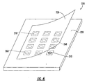
- FIG. 7 is a MEMS valve array 270 wherein apertures 210 are defined within the substrate 220 in a predetermined arrangement and the moveable membrane 230 has a shaped electrode element 280 (outlined in FIG.7 by the broken double lines) that allows for the amount of membrane uncurling to be proportional to the amount of voltage supplied to the electrode element.
- supplying full voltage to the electrode element will cause the moveable membrane to fully uncurl thus sealing-off all valves in the array.
- the membrane may uncurl partially, thus sealing-off only those valves underlying the uncurled portion of the membrane.
- the shape of the electrode element is shown by way of example.
- the shape of the electrode element will be predetermined based upon size of the moveable membrane, size of the array and the configuration of the array. Alternately, the shaped electrode can be the substrate electrode. Shaping the substrate electrode, as opposed to the membrane electrode, may be preferred to insure uniform curl in the moveable membrane.
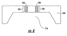
- FIGS. 8-11 illustrate various stages in the fabrication of the MEMS electrostatic valve.
- This method in which initial aperture formation commences prior to the valve construction and is completed after valve construction, has the advantage of allowing the.alignment between the aperture and the surrounding substrate electrode to be performed on the frontside of the substrate construct Since the moveable membrane needs to be formed so that it overlies the aperture, the final opening of the aperture will be completed after the formation of the membrane.
- the thin film nature of the fabrication technology requires that the build surfaces be generally flat prior to forming the substrate electrode and the flexible electrode element of the membrane.
- FIG. 8 is an illustration of a cross-sectional view of a substrate 300 that has undergone backside etch to define a large cavity 310 and front side etch to define valve apertures 320 .
- a large cavity may be defined in the backside of the substrate.
- a conventional wet etch process will be used to form the large cavity.
- the large cavity typically, results in thinning the substrate down to approximately 50 micrometers, although other desirable thicknesses are also possible.
- the large cavity etch process is an optional process that provides for minimization of flow restrictions and simplifies the subsequent formation of the valve apertures.
- the valve apertures are etched partially through the frontside of the substrate.
- RIE reactive ion etch
- FIG. 9 depicts a cross-sectional view of the MEMS valve construct after the valve structure has been formed on the frontside surface of the substrate.
- the formation of the valve structure will include disposing an insulator layer 340 on the substrate; disposing, patterning and etching a substrate electrode layer 350 on the insulator layer; and disposing a dielectric layer 360 on the substrate electrode layer.
- the formation of these layers is followed by the formation of a release layer 370 , typically an oxide that will subsequently be removed to facilitate release of a portion of the membrane from the substrate.
- the membrane 380 is then disposed on the release layer and anchored to the substrate via the dielectric layer.
- the membrane comprises a first biasing element/dielectric layer 390 disposed on the release layer and the dielectric layer, an electrode element layer 400 disposed on the first biasing element/dielectric layer and a second biasing element layer 410 disposed on the electrode.
- first biasing element/dielectric layer 390 disposed on the release layer and the dielectric layer
- electrode element layer 400 disposed on the first biasing element/dielectric layer
- second biasing element layer 410 disposed on the electrode.
- FIG. 10 illustrates a cross-sectional view of the MEMS valve construct after the backside of the substrate has been etched to expose the plug material, the plug material is removed and the aperture 320 has been etched to expose the release layer.
- the backside etch of the substrate is typically performed with a wet etch process. Once the etch process exposes the backside of the sacrificial plug material, the plug is removed by performing an etch process. Typically, the plug material will be removed by a conventional wet etch process. After the plug material has been removed, the aperture is furthered formed into the valve construct up to the release layer 370 . A reactive ion etch process will, typically, be used to further form the aperture and insure that the aperture has precision facings.
- FIG. 11 shows the completed MEMS valve construct after the release layer has been removed, thus, allowing for the distal portion of the membrane to be released from the substrate.
- This method in which initial aperture formation commences prior to the valve construction and is completed after valve construction, has the advantage of allowing the alignment between the aperture and the surrounding substrate electrode to be performed on the frontside of the substrate construct.
Abstract
Description
- The present invention relates to microelectromechanical system (MEMS) valve structures, and more particularly to low-power, high speed electrostatically actuating MEMS valve structures and the associated fabrication methods.
- Advances in thin film technology have enabled the development of sophisticated integrated circuits. This advanced semiconductor technology has also been leveraged to create MEMS (Micro Electro Mechanical System) structures. MEMS structures are typically capable of motion or applying force. Many different varieties of MEMS devices have been created, including microsensors, microgears, micromotors, and other microengineered devices. MEMS devices are being developed for a wide variety of applications because they provide the advantages of low cost, high reliability and extremely small size.
- Design freedom afforded to engineers of MEMS devices has led to the development of various techniques and structures for providing the force necessary to cause the desired motion within microstructures. For example, microcantilevers have been used to apply rotational mechanical force to rotate micromachined springs and gears. Electromagnetic fields have been used to drive micromotors. Piezoelectric forces have also been successfully been used to controllably move micromachined structures. Controlled thermal expansion of actuators or other MEMS components has been used to create forces for driving microdevices. One such device is found in United States Patent No. 5,475,318 entitled "Microprobe" issued December 12, 1995 in the name of inventors Marcus et al., which leverages thermal expansion to move a microdevice. A micro cantilever is constructed from materials having different thermal coefficients of expansion. When heated, the bimorph layers arch differently, causing the micro cantilever to move accordingly. A similar mechanism is used to activate a micromachined thermal switch as described in United States Patent No. 5,463,233 entitled "Micromachined Thermal Switch" issued October 31, 1995 in the name of inventor Norling.
- Electrostatic forces have also been used to move structures. Traditional electrostatic devices were constructed from laminated films cut from plastic or mylar materials. A flexible electrode was attached to the film, and another electrode was affixed to a base structure. Electrically energizing the respective electrodes created an electrostatic force attracting the electrodes to each other or repelling them from each other. A representative example of these devices is found in United States Patent No. 4,266,339 entitled "Method for Making Rolling Electrode for Electrostatic Device" issued May 12, 1981 in the name of inventor Kalt. These devices work well for typical motive applications, but these devices cannot be constructed in dimensions suitable for miniaturized integrated circuits, biomedical applications, or MEMS structures.
- MEMS electrostatic devices are used advantageously in various applications because of their extremely small size. Electrostatic forces due to the electric field between electrical charges can generate relatively large forces given the small electrode separations inherent in MEMS devices. An example of these devices can be found in United States Patent Application No. 09/345,300 entitled "ARC resistant High Voltage Micromachined Electrostatic Switch" filed on June 30, 1999 in the name of inventor Goodwin-Johansson and Untied States Patent Application No. 09/320,891 entitled "Micromachined Electrostatic Actuator with Air Gap" filed on May 27, 1999 in the name of inventor Goodwin-Johansson. Both of these applications are assigned to MCNC, the assignee of the present invention.
- Typical MEMS valves have employed thermal actuation/activation methods to control valves with high flow rates (i.e. large apertures and large clearance areas around the aperture). Thermal actuation has been preferred because it is able to provide the large forces necessary to control the valve over the requisite large distances. However, these valves have relatively slow operation rates due to the thermal time constraints related to the valve materials. Additionally, thermally activated MEMS valves use resistive heating where the power consumed is calculated by the current squared times the resistance and considerable power is consumed in operating the valve.
- US 5,441,597 (Bonne et al) discloses a process for fabricating a flow control device which includes a flexible membrane forming a partition between a main flow passage and a control chamber.
- US 5,771,902 (Lee at all) discloses devices for navigation of endovascular guidewires and/or catheters including micromachined cantilevered actuators, rudders, microvalves, force sensors and positioning or steering mechanisms.
- It would be advantageous to construct a MEMS valve device using electrostatic actuation that is capable of both large displacements and large forces. The electrostatic nature of the MEMS valve will allow for relatively low power consumption and, therefore, no unwarranted heating of the flowing gas or fluid would occur. Additionally, the electrostatic valve will provide for relatively fast operation, allowing for more precise control of the open and closed states of the valve. In addition, it would be advantageous to develop a MEMS valve that forms a secure valve seat to valve cover interface to assure low leakage rates are realized. It would also be beneficial to provide for a MEMS valve that minimizes the occurrence of stiction between the substrate and moveable membrane. Stiction, which is a well-known concept in microelectronics, is defined as the tendency for contacting MEMS surfaces to stick to one another. Stiction is especially a concern in valve devices in which a pressure differential exists across the closed valve. It would be beneficial to devise a MEMS valve that relieves the pressure differential prior to opening the valve.
- As such, MEMS electrostatic valves that have improved performance characteristics are desired for many applications. For example, micromachined valves capable of fast actuation, large valve force and large valve flap displacements that utilize minimal power are desirable, but are currently unavailable.
- The present invention provides for improved MEMS electrostatic valves that benefit from large valve force, fast actuation and large displacement of the moveable membrane to allow for the efficient transport of increased amounts of gas or liquid through the valve. Further, methods for making the MEMS electrostatic valve according to the present invention are provided.
- A MEMS valve device driven by electrostatic forces is provided as claimed in claim 1.
- In one embodiment of the MEMS valve device according to the present invention the resiliently compressible dielectric layer is formed on the substrate electrode and provides for the valve seat surface. In another embodiment of the present invention the resiliently compressible dielectric layer is formed on the moveable membrane and provides for the valve seal surface. In yet another embodiment resiliently compressible dielectric layers are formed on both the substrate electrode and the moveable membrane and provide for both the valve seat surface and the valve seal surface. The resiliently compressible nature of the dielectric layer allows for a secure closed valve to form that benefits from a low leakage rate.
- In yet another embodiment the resiliently compressible dielectric layer has a textured surface; either at the valve seat, the valve seal or at both surfaces. By texturing these surfaces the valve is able to overcome stiction that causes the MEMS films to stick together after the electrostatic voltage is removed. In effect, texturing reduces the surface area around the valve seat to seal interface thereby reducing the effects of stiction. Additionally, texturing allows pressure to be advantageously used in easing the opening of the valve.
- In another embodiment of the invention a pressure-relieving aperture is defined within the planar substrate and is positioned to underlie the moveable membrane. The pressure-relieving aperture provides a decrease in the pressure differential across the valve aperture by alleviating pressure prior to the opening of the valve.
- Alternatively, another embodiment of the present invention provides for a MEMS valve array driven by electrostatic forces as claimed in
claim 20. The array configuration allows for increased gas or liquid flows. - In another embodiment of the array, the substrate has a plurality of apertures and a plurality of substrate electrodes is provided; wherein each aperture has a corresponding substrate electrode. In this manner, the substrate electrodes can be individually supplied electrostatic voltages, thus controlling the number of apertures opened or closed. This configuration effectuates a variable flow rate valve.
- Additionally, the array of the present invention is embodied in a substrate having a plurality of apertures and a shaped electrode element within the moveable membrane and/or the substrate. The shaped nature of the electrode element allows for the amount of membrane uncurling to be adjusted in accordance with the amount of voltage applied between the electrodes.
- An example provides a method for making the MEMS valve device described above. The method comprises the steps of etching the frontside of a substrate to define an aperture extending partially through the substrate, filling the aperture with a plug material, forming a membrane valve structure on the frontside of the substrate, removing the plug material, etching the backside of the valve aperture up to the release layer and removing the release layer to at least partially release the membrane from the substrate. The method provided allows for the alignment of the aperture and the substrate electrode to be accomplished on the frontside of the substrate.
- As such the MEMS valve device driven by electrostatic force is capable of both large displacements and large forces. The electrostatic nature of the MEMS valve allows for relatively low power consumption and, therefore, no unwarranted heating of the flowing gas or fluid occurs. Additionally, the electrostatic valve will provide for relatively fast operation, allowing for faster cycle time and more precise control of the open and closed states. Furthermore, the MEMS valve provides for a secure valve seat to valve cover interface to assure low leakage rates. An additional benefit is realized in providing for a MEMS valve that minimizes the occurrence of stiction between the substrate and moveable membrane. Stiction is overcome by providing for textured surfaces at the valve seat and/or valve seal interface or allowing for a pressure-relieving aperture to be defined in the substrate. These and many more advantages can be realized with the MEMS valve device of the present invention.
-
- FIG. 1 is a cross-sectional view of a MEMS electrostatic valve in accordance with an embodiment of the present invention.
- FIG. 2 is a top plan view of a MEMS electrostatic valve in accordance with an embodiment of the present invention.
- FIG. 3 is a cross-sectional view of a MEMS electrostatic valve having an air gap between the substrate and the moveable membrane in accordance with an embodiment of the present invention.
- FIG. 4 is a cross-sectional view of a MEMS electrostatic valve having a decreasing air gap between the substrate and the moveable membrane in accordance with an embodiment of the present invention.
- FIG. 5 is a perspective view of a MEMS electrostatic valve array having individual moveable membranes associated with array apertures.
- FIG. 6 is a perspective view of a MEMS electrostatic valve array having individual substrate electrodes associated with array apertures in accordance with an alternate embodiment of the present invention.
- FIG. 7 is a perspective view of a MEMS electrostatic valve array having a shaped electrode element within the moveable membrane in accordance with an alternate embodiment of the present invention.
- FIGS. 8 - 11 are cross-sectional views of a MEMS valve construct during various stages of fabrication.
- The present invention now will be described more fully hereinafter with reference to the accompanying drawings, in which preferred embodiments of the invention are shown. This invention may, however, be embodied in many different forms and should not be construed as limited to the embodiments set forth herein; rather, these embodiments are provided so that this disclosure will be thorough and complete, and will fully convey the scope of the invention to those skilled in the art. Like numbers refer to like elements throughout.
- Referring to FIGS. 1 and 2, a cross-sectional view (FIG. 1) and a top view of the substrate construct (FIG. 2) of an embodiment of the present invention provides a
MEMS valve device 10 driven by electrostatic forces that can provide high and variable flow rates. As shown in FIG. 1, the layers of the MEMS valve device construct are arranged and shown vertically. In a first embodiment, an electrostatic MEMS valve device comprises in layers, a generallyplanar substrate 20, asubstrate insulator 30, asubstrate electrode 40, asubstrate dielectric 50, and amoveable membrane 60. The substrate defines anaperture 70 formed therethrough that serves as the valve opening, In the embodiment shown the aperture is formed in cooperation with the substrate, the substrate insulator, the substrate electrode and the substrate dielectric. In this manner, the aperture may be formed through the substrate, the substrate insulator, the substrate electrode and/or the substrate dielectric. It is also possible and within the inventive concepts herein disclosed to form the aperture in various other configurations that allow for the flowable media (i.e. gas, liquid, light, etc.) to enter at one side of the substrate construct and exit at the opposite side of the substrate construct. Typically, the aperture will be cylindrical in shape. However, other shapes such as, a funnel shape having a smaller perimeter at the valve seat and a larger perimeter at the backside opening of the substrate, are also possible and within the breadth of the invention disclosed. - The movable membrane may be described as having two portions referred to as the fixed
portion 80 and thedistal portion 90. The portions are deposited horizontally along the length of the moveable membrane. The fixed portion is substantially affixed to the underlying substrate or intermediate layers at theattachment point 100. The distal portion is released from the underlying substrate or intermediate layers during fabrication of the MEMS valve device. During MEMS device operation the distal portion of the device is moveable with respect to the underlying substrate and substrate electrode. The movement of the distal portion thereby controllably adjusts the portion of the aperture covered by the moveable membrane. - In the FIG. 1 cross-sectional view, the
moveable membrane 60 comprises multiple layers including at least oneelectrode element layer 62 and at least one biasingelement layer 64 and/or 66. The biasing element(s) provide the moveable membrane with the biased shape shown in FIG.1. Once the moveable membrane is released from the substrate during fabrication, the biasing element allows the overall membrane structure to position itself distant from the substrate. In the embodiment shown in FIG. 1 biasing provides for the upward curled shape of the moveable membrane. Biasing can be accomplished by providing for materials of dissimilar coefficients of thermal expansion, materials having substantive differences in cross-sectional thickness or other material characteristics may also effect biasing. The electrode element provides the moveable membrane with a means for electrostatic actuation. In valve operation a voltage is supplied to the electrode element and it is electrostatically attracted toward the substrate electrode. As the electrode element comes in contact with the substrate construct, the moveable membrane forms a valve seal that serves to seal-off the aperture formed in the substrate. - The electrostatic MEMS valve device, including the moveable membrane and underlying substrate layers, is constructed using known integrated circuit materials and microengineering techniques. Those skilled in the art will understand that different materials, various numbers of layers, and numerous arrangements of layers may also be used to form the underlying substrate layers and the moveable membrane. Although the MEMS valve device illustrated in the figures will be used as an example to describe manufacturing details, this discussion applies equally to all MEMS valve devices provided by the present invention unless otherwise noted.
- Referring to FIGS. 1 and 2, a
substrate 20 defines a generallyplanar surface 22 upon which the electrostatic MEMS valve device is constructed. Preferably the substrate comprises a microelectronic substrate, such as silicon, although any suitable substrate material having a generally planar surface can be used. The further processing steps involved in the fabrication of the present invention may be performed at relatively low temperatures and, therefore, the substrate that is used is not limited to conventional higher temperature substrates. By way of example, quartz, glass, or other suitable materials having insulating tendencies may serve as the substrate. Asubstrate insulator layer 30 typically overlies the planar surface of the substrate and provides electrical isolation. In certain embodiments that implement substrate materials having strong insulation characteristics it may be possible to form the MEMS valve device without the substrate insulator layer. The substrate insulator layer preferably comprises a non-oxidation-based insulator or polymer, such as polyimide or nitride. In this application, oxide based insulators are avoided if certain acids (such as hydrofluoric acid) are used in processing to remove the release layer. The substrate insulator layer is preferably formed by using a standard deposition technique, such as conventional spinning or low-pressure chemical vapor deposition (LPCVD), to deposit the insulating layer on the planar surface of the substrate. - A
substrate electrode 40 is deposited as a generally planar layer affixed to at least a portion of the surface of the underlyingsubstrate insulator layer 30 orsubstrate 20. The substrate electrode preferably comprises a gold layer deposited on the top surface of the insulator layer. If the substrate electrode is formed from a layer of gold, optionally a thin layer of chromium may be deposited prior to depositing the substrate signal electrode layer to allow better adhesion to the insulating layer and/or after the substrate signal electrode layer has been deposited to allow better adhesion to any subsequent adjacent materials. Alternatively, other suitable metallic or conductive materials may be used for the substrate signal electrode so long as release layer processing operations does not result in electrode erosion. Standard photolithography and etching techniques are typically used to deposit the electrode on the surface of the substrate. - Once the substrate electrode has been formed, preferably, a
substrate dielectric layer 50 is deposited on the substrate electrode to provide for a dielectric that electrically isolates the substrate signal from the electrode element found in the moveable membrane. In embodiments that employ a substrate dielectric layer, this layer serves as thevalve seat 52 that surrounds the valve aperture. In a preferred embodiment the substrate dielectric layer will comprise a resiliently compressible material. Resiliency for any given material can be assessed by comparing (a) the ratio of the electrostatic force of the valve around the aperture to the valve seat area (i.e. the applied pressure) versus (b) the product of Young's modulus (measure of elasticity) for the given material and the ratio of the surface roughness of the valve seat to the thickness of the valve seat. The resiliently compressible nature of the substrate dielectric layer will allow for the valve seat to deform upon contact with the moveable membrane. The deforming characteristic of the valve seat provides for a sound valve seal to form, thus providing for improved off-flow. One such resiliently compressable substrate dielectric material comprises polyimide, although other resiliently compressible dielectric insulators or polymers tolerant of release layer processing may also be used. The substrate dielectric layer is formed using a conventional deposition technique, such as standard spinning techniques or low-pressure chemical vapor deposition LPCVD. - The
substrate dielectric layer 50 may be formed with a generally planar surface (as shown in FIG.1) or the substrate dielectric layer may be formed with a textured surface. A textured surface at thevalve seat 52 area may be preferred in those embodiments in which the moveable membrane "sticks" to the underlying substrate when release is desired. The MEMS phenomena related to the tendency of two mating MEMS surfaces to stick together is known in the art as stiction. By providing for a textured surface at the valve seat less surface area is contacting the moveable membrane when the valve seal is closed and thus less force is necessary to overcome the stiction. Textured surfaces are typically formed during fabrication and the implementation and fabrication of such surfaces is well known in the art. - A release layer (not shown in FIGS. 1 and 2), is deposited on the surface of the
substrate dielectric layer 50 in the area generally underneath the distal portion of the overlying moveable membrane. The release layer is only deposited on those regions below moveable membrane portions not being affixed to the underlying substrate structure. Preferably, the release layer comprises an oxide or other suitable material that may be etched away when acid is applied thereto. After the overlying layers of the moveable membrane have been deposited on the substrate, the release layer may be removed through standard microengineering acidic etching techniques, such as a hydrofluoric acid etch. When the release layer has been removed, thedistal portion 90 ofmoveable membrane 60 is separated from the underlying surface. The release of the moveable membrane from the substrate in conjunction with the biasing characteristics of the biasing element will typically result in the thin film membrane having a distal portion that has a curled shape. Biasing in the moveable membrane will typically result in the moveable membrane curling away from the substrate (as shown in FIG.1) when no electrostatic force is applied. It is also possible to bias the moveable membrane such that it curls toward the substrate when no electrostatic force is applied. - Biasing in the moveable membrane may be accomplished by providing for biasing element and electrode element materials that differ in thickness, thermal coefficient of expansion or any other known biasing characteristic. Alternately, biasing may be induced during fabrication by employing process steps that create intrinsic stresses so as to curl the moveable membrane. For example, a polymeric biasing element can be deposited as a liquid and then cured by elevated temperatures so that it forms a solid biasing layer. Preferably, the biasing element may comprise a polymer material having a higher thermal coefficient of expansion than the electrode element. Next, the biasing element and the electrode element are cooled, inducing stresses in the membrane due to differences in the thermal coefficients of expansion. The moveable membrane curls because the polymeric biasing element shrinks faster than the electrode layer.
- Additionally, providing differential thermal coefficients of expansion between the biasing element layers and the electrode element layer can create bias. Assuming an increase in temperature, the moveable membrane will curl toward the layer having the lower thermal coefficient of expansion because the layers accordingly expand at different rates. As such, the moveable membrane having two layers with different thermal coefficients of expansion will curl toward the layer having a lower thermal coefficient of expansion as the temperature rises. In addition, two polymer film layers having different thermal coefficients of expansion can be used in tandem with an electrode layer to bias the moveable membrane as necessary.
- The layers of the
moveable membrane 60 generally overlie thesubstrate electrode 40 and theaperture 70. Known integrated circuit manufacturing processes are used to construct the layers comprisingmoveable membrane 60. The moveable membrane is comprised of an electrode element and a biasing element. Preferably, one or more layers of the moveable membrane comprise the electrode element and one or more additional layers comprise the biasing element. As shown in FIG.1, one preferred embodiment of the moveable membrane comprises anelectrode element layer 62 positioned between two biasing element layers 64 and 66. It is also possible to configure the moveable membrane with an electrode element layer having only one biasing layer positioned on either side of the electrode element layer. The biasing element layer may also serve as an insulator that allows for the complete electrical isolation between the substrate electrode and the electrode element of the moveable membrane. - Preferably, at least one of the layers comprising the moveable membrane is formed from a flexible material, for instance flexible polymers (i.e: the biasing element) and/or flexible conductors (i.e. the electrodes) may be used. In a preferred embodiment the biasing element will comprise a flexible polymer film used to hold the moveable membrane in a stationary position absent electrostatic forces. In those applications in which the biasing element contacts the substrate to form the valve seal the biasing element comprises a resiliently compressible material. The resiliently compressible nature of the biasing element layer will allow for the valve seal to deform upon contact with the underlying substrate structure. The deforming characteristic of the contacting biasing element surface provides for a sound valve seal to form, thus providing for improved off-flow. A polymer film material that has resiliently compressible characteristics may include a polyimide material, however, other suitable flexible polymers having resilient characteristics and capable of withstanding the release layer etch process can also be employed. In one embodiment both the substrate dielectric layer and the biasing element layer of the moveable membrane are formed of a resiliently compressible material, such as a polyimide material.
- The use of polyimide materials in the moveable membrane has been shown to withstand the pressure generated across the aperture that the membrane is intended to seal. Additionally, the strength of polyimide materials has shown to be resistant to rupturing or blistering even after prolonged use. Calculations have shown that the deflection of a polyimide membrane over a hole having a circumference of 80 micrometers with a pressure difference of 300 psi is approximately 0.064 micrometers for a 3 micrometer membrane and 0.22 micrometers for a 2 micrometer membrane. These calculations do not take into account the electrode element layer that will invariably further limit the amount of deflection of the overall moveable membrane.
- The
electrode element 62 of themoveable membrane 60 preferably comprises a layer of flexible conductor material. The electrode element may be deposited directly upon the uppermost planar surface of the substrate construct and the release layer or over an optional first biasing layer (i.e. polymer film), as needed. The electrode element preferably comprises gold, although other conductors tolerant of release layer processing and other flexible materials, such as conductive polymer film, may be used. The surface area and/or configuration of the electrode element can be varied as required to allow for the desired electrostatic forces to operate the MEMS valve device. By shaping the electrode element in a predetermined fashion it is possible to effectuate changes in the valve release rate. If gold is used to form the electrode element, a thin layer of chromium may be deposited onto the electrode element to allow better adhesion of the gold layer to the adjacent materials, such as to one or more biasing layers of flexible polymer film or the like. - The number of layers, thickness of layers, arrangement of layers, and choice of materials used in the moveable membrane may be selected to bias the moveable membrane as required. In particular, the distal portion can be varyingly biased as it extends from the fixed portion. The biased position of the distal portion can be customized individually or collectively to provide a desired separation from the underlying planar surface and the substrate electrode. For example, the distal portion can be biased to remain parallel to the underlying planar surface. Alternatively, the distal portion can be biased to alter the separation from the underlying planar surface by curling toward or curling away from the underlying planar surface. Preferably, the distal portion biased to curl away from the underlying substrate and alter the separation therefrom. Those skilled in the art will appreciate that more than one polymer film layer may be used, and that the films may be deposited on either side or both sides of the electrode elements.
- When a voltage is applied between the electrode element of the moveable membrane and the substrate electrode, the electrostatic force between the electrode attracts the flexible electrode element towards the substrate, unrolling the moveable membrane to effectuate coverage of the aperture. The close proximity of the two electrodes when the valve is closed results in a strong electrostatic force. This strong electrostatic force results in a valve seal having a low leakage rate. When the voltage is removed from the electrodes, the stress in the film causes the flexible electrode to curl away from the substrate and open the valves. In the open position, since the portion of the membrane that covers the aperture is a relatively large distance from the substrate, large flows through the aperture can be realized without flow restrictions.
- The valve can be configured so that a pressure difference can be applied in either direction across the membrane when the membrane seals the aperture. If the pressure is coming from the backside of the substrate and pushing up against the membrane when the valve is closed, then the pressure will assist in the re-curling of the film when the voltage is removed. If, however, the pressure is coming from the frontside of the substrate and pushing down against the membrane when it is closed, the stress in the membrane will have to work against the applied pressure to open the valve. This pressure build-up can be minimized by providing for a small aperture through the substrate proximate the end of the distal portion of the moveable membrane. Since the stress required to curl up the membrane will be proportional to the overall width of the membrane, the curling stress can be increased in comparison to the pressure exerted at the small pressure-relieving aperture by providing for this small aperture. Once the small pressure-relieving aperture has been opened, the pressure differential across the membrane at the valve aperture will be reduced, making it easier for the stress in the membrane to open the valve. An example of such a pressure-relieving
aperture 102 is shown in FIGS. 1 and 2. - FIG. 3 illustrates a cross-sectional view of an alternative embodiment of the MEMS electrostatic valve in accordance with the present invention. The MEMS
electrostatic valve 10 of this embodiment has a characteristicallyuniform air gap 110 underlying amedial portion 120 of themoveable membrane 60. The medial portion of the moveable membrane is defined as the horizontal region between the fixedportion 80 and thedistal portion 90. A release layer (not shown in FIG. 3) is deposited on the uppermost layer of the substrate construct in the area underlying the medial and distal portions of the moveable membrane. The release layer is subsequently removed and results in the overall spatial separation between the medial and distal portions of the membrane and the underlying substrate. - The medial portion is constructed generally similar in make-up to the distal portion and, therefore, the differential in thermal coefficients of expansion between the electrode element and the biasing element cause the medial portion to exhibit curling. The curling nature of the moveable membrane is desired for the distal portion, but is generally undesirable for the medial portion. It is important to provide for a predictable medial portion, and thus a predictable air gap, because predictability lends itself to improved operating voltage characteristics. To alleviate the tendency for the medial portion to curl, a
bias control layer 130 is typically provided for that overlies the fixed and medial portions of the moveable membrane and structurally constrains the medial portion. Typically, the bias control layer will overlay the fixed and medial portion of the membrane and extend outward, over the sides of the membrane, in order to allow for the bias control layer to be anchored to the substrate. The biasing control layer can be formed from a metallic material and will generally have a thermal coefficient of expansion that differs from the underlying membrane materials so as to hold the medial portion in a stationary position. The biasing control layer may be a generally solid layer, or it may comprise, lines, grids, cross-hatchings, or other patterns as required to support the medial portion and control the shape of the air gap. - Alternatively, the
medial portion 120 of themoveable membrane 60 can be restrained during release by implementing tabs 104 (shown in the plan view perspective of FIG. 2) on the moveable membrane at the fixedportion 80. The tabs, which are typically extensions of the layers that comprise the membranes, provide an added holding force to insure that a uniform air gap is provided for under the medial portion. The tabs may be formed from one or more layers that comprise the moveable membrane. - FIG. 4 illustrates a cross-sectional view of yet another alternative embodiment of the MEMS electrostatic valve in accordance with the present invention. The MEMS
electrostatic valve 10 of this embodiment has a characteristic decreasingair gap 150 underlying amedial portion 120 of themoveable membrane 60. In this embodiment the cantilevered portion slopes downward until it contacts the underlying substrate construct at which point the moveable membrane transitions into the distal portion and the membrane curls away from the underlying planar surface. By way of example, the sloping medial portion may be fabricated by patterning the biasing layer so as to effect a thin region at theinflection area 160 or patterning the sloping region of the medial portion to cause the medial portion to slope toward the substrate. - By predefining the shape of the air gap, recently developed MEMS electrostatic devices can operate with lower and less erratic operating voltages. Further discussion of recently development MEMS electrostatic devices having predefined air gaps is being omitted from this disclosure so as not to overcomplicate the present invention. For an example of a recently developed improved MEMS device, see United States Patent Application No. 09/320,891, entitled "Micromachined Electrostatic Actuator with Air Crap" filed on May 27, 1999, in the name of inventor Goodwin-Johansson and assigned to MCNC, the assignee of the present invention.
- Increased gas or liquid flows can be achieved by creating an array of apertures defined with a single substrate. FIGS. 6 - 7 illustrate perspective views of various MEMS electrostatic valve arrays in accordance with further embodiments of the present invention. FIG. 5 is a
MEMS valve array 200 shown for background information whereinapertures 210 are defined within thesubstrate 220 in a predetermined arrangement and each valve aperture has a correspondingmoveable membrane 230. By selectively addressing electrode elements within the individual membranes variable flow rates can be obtained by controlling the number of valves opened and closed. - FIG. 6 is a
MEMS valve array 250 whereinapertures 210 are defined within thesubstrate 220 in a predetermined arrangement and each valve aperture has a corresponding fixed substrate electrode disposed on the substrate. By selectively addressing the fixedsubstrate electrodes 260 within the substrate variable flow rates can be obtained by controlling the number of valves opened and closed. With a single largemoveable membrane 230 this will typically involve supplying voltage to a row(s) of apertures. Rows in this context are defined as lines of apertures running perpendicular to the lengthwise direction of the moveable membrane. For example if electrostatic voltage is supplied to the substrate electrodes associated with the row of apertures nearest the fixed portion of the valve structure, the moveable membrane will be pulled down to seal-off these apertures and the remaining distal portion of the membrane will maintain a curled position. Additionally, an array of this nature may provide for the rows of apertures to be canted, at a slight angle, with respect to the underlying rows of substrate electrodes to provided for a greater degree of variable flow as opposed to step-like changes in flow. - FIG. 7 is a
MEMS valve array 270 whereinapertures 210 are defined within thesubstrate 220 in a predetermined arrangement and themoveable membrane 230 has a shaped electrode element 280 (outlined in FIG.7 by the broken double lines) that allows for the amount of membrane uncurling to be proportional to the amount of voltage supplied to the electrode element. In this regard, supplying full voltage to the electrode element will cause the moveable membrane to fully uncurl thus sealing-off all valves in the array. In instances where less than full voltage is supplied the membrane may uncurl partially, thus sealing-off only those valves underlying the uncurled portion of the membrane. The shape of the electrode element is shown by way of example. The shape of the electrode element will be predetermined based upon size of the moveable membrane, size of the array and the configuration of the array. Alternately, the shaped electrode can be the substrate electrode. Shaping the substrate electrode, as opposed to the membrane electrode, may be preferred to insure uniform curl in the moveable membrane. - FIGS. 8-11 illustrate various stages in the fabrication of the MEMS electrostatic valve. This method, in which initial aperture formation commences prior to the valve construction and is completed after valve construction, has the advantage of allowing the.alignment between the aperture and the surrounding substrate electrode to be performed on the frontside of the substrate construct Since the moveable membrane needs to be formed so that it overlies the aperture, the final opening of the aperture will be completed after the formation of the membrane. The thin film nature of the fabrication technology requires that the build surfaces be generally flat prior to forming the substrate electrode and the flexible electrode element of the membrane.
- FIG. 8 is an illustration of a cross-sectional view of a
substrate 300 that has undergone backside etch to define alarge cavity 310 and front side etch to definevalve apertures 320. Initially, a large cavity may be defined in the backside of the substrate. Typically, a conventional wet etch process will be used to form the large cavity. The large cavity, typically, results in thinning the substrate down to approximately 50 micrometers, although other desirable thicknesses are also possible. The large cavity etch process is an optional process that provides for minimization of flow restrictions and simplifies the subsequent formation of the valve apertures. After the large cavity is formed, the valve apertures are etched partially through the frontside of the substrate. Typically a reactive ion etch (RIE) process will used to perform the precision etching required of the valve apertures. Asacrificial plug material 330 is then disposed in the apertures to facilitate a continuous substrate layer upon which the valve can be constructed. The sacrificial plug material will typically comprise copper or any other suitable material may be used as the sacrificial plug material. Once the plug material has been disposed, it is typically subjected to a polishing procedure to assure planarization of the surface and ready the substrate for valve construction. - FIG. 9 depicts a cross-sectional view of the MEMS valve construct after the valve structure has been formed on the frontside surface of the substrate. Typically, the formation of the valve structure will include disposing an
insulator layer 340 on the substrate; disposing, patterning and etching asubstrate electrode layer 350 on the insulator layer; and disposing adielectric layer 360 on the substrate electrode layer. The formation of these layers is followed by the formation of arelease layer 370, typically an oxide that will subsequently be removed to facilitate release of a portion of the membrane from the substrate. Themembrane 380 is then disposed on the release layer and anchored to the substrate via the dielectric layer. In the embodiment shown, the membrane comprises a first biasing element/dielectric layer 390 disposed on the release layer and the dielectric layer, anelectrode element layer 400 disposed on the first biasing element/dielectric layer and a secondbiasing element layer 410 disposed on the electrode. These valve construct layers and fabrication steps are shown by way of example. The surfaces that will eventually form the valve seat and the valve cover may be textured surfaces to allow for the MEMS device to overcome common release problems related to stiction. In the embodiment shown it may be desirable to texture thedielectric layer 360 and/or the first biasing element/dielectric layer 390. The texturing of these surfaces can be accomplished in conjunction with the deposition and removal of the release layer. The process of texturing a surface on a MEMS device is well known by those of ordinary skill in the art. - FIG. 10 illustrates a cross-sectional view of the MEMS valve construct after the backside of the substrate has been etched to expose the plug material, the plug material is removed and the
aperture 320 has been etched to expose the release layer. The backside etch of the substrate is typically performed with a wet etch process. Once the etch process exposes the backside of the sacrificial plug material, the plug is removed by performing an etch process. Typically, the plug material will be removed by a conventional wet etch process. After the plug material has been removed, the aperture is furthered formed into the valve construct up to therelease layer 370. A reactive ion etch process will, typically, be used to further form the aperture and insure that the aperture has precision facings. FIG. 11 shows the completed MEMS valve construct after the release layer has been removed, thus, allowing for the distal portion of the membrane to be released from the substrate. - This method, in which initial aperture formation commences prior to the valve construction and is completed after valve construction, has the advantage of allowing the alignment between the aperture and the surrounding substrate electrode to be performed on the frontside of the substrate construct.
- Many modifications and other embodiments of the invention will come to mind to one skilled in the art to which this invention pertains having the benefit of the teachings presented in the foregoing descriptions and the associated drawings.
Claims (23)
- A MEMS (Micro Electro Mechanical System) valve driven by electrostatic forces, comprising:a substrate (20) having a generally planar surface (22) having an aperture (70) formed therein;a substrate electrode (40) disposed upon said planar surface (22) of said substrate (20),a moveable membrane (60) generally overlying said aperture (70) in an uncurled state and fully supported by the substrate (20), the moveable membrane (60) comprising an electrode element (62) and a biasing element (64), wherein the moveable membrane (60) includes a fixed portion (80) attached to said planar surface (22) of said substrate (20) and a distal portion (90) adjacent to the fixed portion (80), the distal portion (90) being in a curled state absent electrostatic force and moveable via electrostatic force with respect to said substrate electrode (40); andat least one resiliently compressible dielectric layer (50) disposed between said substrate electrode (40) and said membrane electrode element (62),wherein said resiliently compressible dielectric layer (50) is a polymeric dielectric layer,
wherein the substrate electrode (40) extends laterally throughout an area overlaid by said moveable membrane (60), and said membrane (60) is configured to move from said curled state to a generally uncurled state in response to a voltage differential established between said substrate electrode (40) and said moveable membrane electrode (62). - The MEMS valve of Claim 1, wherein said at least one polymeric dielectric layer (50) comprises a first polymeric dielectric layer (50) disposed on said substrate electrode (40), wherein said substrate (20), said substrate electrode (40) and said first polymeric dielectric layer (50) cooperate to define the aperture therethrough and said first polymeric dielectric layer (50) defines a valve seat (52).
- The MEMS valve of Claim 2, wherein said first polymeric dielectric layer (50) comprises a textured valve seat surface, wherein the textured valve seat surface facilitates release of the moveable membrane (60) from said planar surface (22) of the said substrate (20) during valve operation.
- The MEMS valve of Claim 2, wherein said first polymeric dielectric layer (50) comprises a polyimide material.
- The MEMS valve of Claim 1, wherein said at least one polymeric dielectric layer (64) is a first polymeric dielectric layer disposed on said moveable membrane (60) and defines a surface that acts as a valve seal.
- The MEMS valve of Claim 5, wherein said first polymeric dielectric layer (64) comprises a textured valve seal surface, wherein the textured valve seal surface facilitates release of the moveable membrane (60) from said planar surface (22) of the said substrate (20) during valve operation.
- The MEMS valve of Claim 5, wherein said first polymeric dielectric layer (64) comprises a polyimide material.
- The MEMS valve of Claim 1, wherein said at least one polymeric dielectric layer (50) comprises a first polymeric dielectric layer (50) disposed on said substrate (20) and a second polymeric dielectric layer (64) disposed on said moveable membrane(60), wherein the first polymeric dielectric layer (50) defines a valve seat (52) and the second polymeric dielectric layer (64) defines a valve seal.
- The MEMS valve of Claim 8, wherein said first polymeric dielectric layer (50) comprises a textured valve seat surface and said second polymeric dielectric layer comprises a textured valve seal surface, wherein the textured valve seal surface and the textured valve seat surface facilitate release of the moveable membrane (60) from said planar surface (22) of the said substrate (20) during valve operation.
- The MEMS valve of Claim 8, wherein said first and second polymeric dielectric layers (50,64) comprise polyimide materials.
- The MEMS valve of Claim 1, wherein said aperture (70) is generally funnel-like in shape, having a smallest radius nearest the moveable membrane (60).
- The MEMS valve according to Claim 1, wherein said biasing element (64) comprises at least one polymer film layer.
- The MEMS valve according to Claim 1, wherein said biasing element (64) comprises two polymer film layers (64,66) deposited on opposite sides of an electrode layer comprising said electrode element.
- The MEMS valve according to Claim 1, wherein said electrode element (62) and said biasing element (64) have different thermal coefficients of expansion so as to impart curl in said moveable membrane (60) absent electrostatic force.
- The MEMS valve according to Claim 1, wherein said biasing element (64) comprises at least two polymer films of different thickness so as to impart curl in said moveable membrane (60) absent electrostatic force.
- The MEMS valve according to Claim 15, wherein said at least two polymer films of different thickness comprise a first polymer film (64) having a thinner thickness deposited on a surface of the electrode element (62) nearest said substrate and a second polymer film (66) having a thicker thickness deposited on a surface of the electrode element (62) furthest from said substrate.
- The MEMS valve device according to Claim 1, wherein said biasing element (64) comprises at least two polymer films of different coefficients of expansion so as to impart curl in said moveable membrane absent electrostatic force.
- The MEMS valve according to Claim 1, further comprising a source of electrostatic energy electrically connected to at least one of said substrate electrode (40) and said electrode element (62).
- The MEMS valve according to Claim 1, wherein said substrate (20) further defines a pressure-relieving aperture that underlies said moveable membrane (60).
- A MEMS valve array (250) driven by electrostatic forces, comprising:a substrate (220) having a generally planar surface having a plurality of apertures (210) formed therein;a substrate electrode (260) disposed upon said planar surface of said substrate,a single moveable membrane (230) generally overlying said plurality of apertures in an uncurled state and fully supported by said substrate, the moveable membrane comprising an electrode element and a biasing element, wherein the moveable membrane (230) includes a fixed portion attached to said planar surface of said substrate and a distal portion adjacent to the fixed portion, the distal portion being in a curled state absent electrostatic force and moveable via electrostatic force with respect to said substrate electrode; andat least one resiliently compressible dielectric layer disposed between said substrate electrode and said electrode element,wherein said resiliently compressible dielectric layer is a polymeric dielectric layer,
wherein said membrane (230) is configured to move from said curled state to a generally uncurled state in response to a voltage differential established between said substrate electric and said moveable membrane electrode. - The MEMS valve array of Claim 20, wherein said substrate electrode further comprises a plurality of substrate electrodes (260) disposed upon said planar surface of said substrate (220), wherein said plurality of substrate electrodes (260) and said substrate (220) cooperate to define a plurality of apertures (210) therethrough and each substrate electrode has a corresponding aperture,
whereby a voltage differential established between one or more of the plurality of said substrate electrodes and said electrode element moves said membrane (230) from said curled state to a generally uncurled state to thereby controllably adjust one or more of said plurality of apertures (210) covered by said moveable membrane (230). - The MEMS valve array of Claim 21, wherein the plurality of apertures (210) are positioned in rows that extend generally perpendicular to a lengthwise direction of the moveable membrane (230).
- The MEMS valve array of Claim 22, wherein the rows of apertures (210) are generally canted at a predetermined angle with respect to the corresponding substrate electrode (260) to provide variable flow.
Applications Claiming Priority (3)
| Application Number | Priority Date | Filing Date | Title |
|---|---|---|---|
| US661997 | 2000-09-14 | ||
| US09/661,997 US6590267B1 (en) | 2000-09-14 | 2000-09-14 | Microelectromechanical flexible membrane electrostatic valve device and related fabrication methods |
| PCT/US2001/028608 WO2002022492A2 (en) | 2000-09-14 | 2001-09-14 | Microelectromechanical flexible membrane electrostatic valve device and related fabrication methods |
Publications (2)
| Publication Number | Publication Date |
|---|---|
| EP1317399A2 EP1317399A2 (en) | 2003-06-11 |
| EP1317399B1 true EP1317399B1 (en) | 2006-08-30 |
Family
ID=24655972
Family Applications (1)
| Application Number | Title | Priority Date | Filing Date |
|---|---|---|---|
| EP01970902A Expired - Lifetime EP1317399B1 (en) | 2000-09-14 | 2001-09-14 | Microelectromechanical flexible membrane electrostatic valve device and related fabrication methods |
Country Status (8)
| Country | Link |
|---|---|
| US (1) | US6590267B1 (en) |
| EP (1) | EP1317399B1 (en) |
| JP (2) | JP2004508952A (en) |
| AT (1) | ATE338010T1 (en) |
| AU (1) | AU2001290851A1 (en) |
| CA (1) | CA2421934C (en) |
| DE (1) | DE60122749T2 (en) |
| WO (1) | WO2002022492A2 (en) |
Families Citing this family (105)
| Publication number | Priority date | Publication date | Assignee | Title |
|---|---|---|---|---|
| US6827584B2 (en) * | 1999-12-28 | 2004-12-07 | Formfactor, Inc. | Interconnect for microelectronic structures with enhanced spring characteristics |
| US6660564B2 (en) * | 2002-01-25 | 2003-12-09 | Sony Corporation | Wafer-level through-wafer packaging process for MEMS and MEMS package produced thereby |
| GB0205794D0 (en) * | 2002-03-12 | 2002-04-24 | Montelius Lars G | Mems devices on a nanometer scale |
| US6859300B2 (en) * | 2002-09-30 | 2005-02-22 | Lucent Technologies Inc. | Monolithic two-axis MEMS device for optical switches |
| US6924581B2 (en) * | 2002-09-30 | 2005-08-02 | Lucent Technologies Inc. | Split spring providing multiple electrical leads for MEMS devices |
| US6850354B2 (en) * | 2002-09-30 | 2005-02-01 | Lucent Technologies Inc. | Monolithic MEMS device for optical switches |
| DE50209239D1 (en) * | 2002-10-17 | 2007-02-22 | Ford Global Tech Llc | Valve device for a motor vehicle |
| DE10257822B3 (en) * | 2002-12-10 | 2004-08-12 | Forschungszentrum Jülich GmbH | Frequency tuning device for a cavity resonator or dielectric resonator |
| US20040118621A1 (en) * | 2002-12-18 | 2004-06-24 | Curtis Marc D. | Live hydraulics for utility vehicles |
| US7195026B2 (en) * | 2002-12-27 | 2007-03-27 | American Air Liquide, Inc. | Micro electromechanical systems for delivering high purity fluids in a chemical delivery system |
| US6807892B2 (en) * | 2002-12-30 | 2004-10-26 | Xerox Corporation | Pneumatic actuator with elastomeric membrane and low-power electrostatic flap valve arrangement |
| DE10302304B3 (en) * | 2003-01-22 | 2004-01-29 | Festo Ag & Co. | Electronic microvalve and method for its operation |
| CA2435538A1 (en) * | 2003-07-18 | 2005-01-18 | Universite Laval | Solvent resistant asymmetric integrally skinned membranes |
| US6930367B2 (en) | 2003-10-31 | 2005-08-16 | Robert Bosch Gmbh | Anti-stiction technique for thin film and wafer-bonded encapsulated microelectromechanical systems |
| JP4552432B2 (en) * | 2003-12-11 | 2010-09-29 | ダイキン工業株式会社 | Compressor |
| WO2005104717A2 (en) * | 2004-04-23 | 2005-11-10 | Research Triangle Institute | Flexible electrostatic actuator |
| US7484940B2 (en) * | 2004-04-28 | 2009-02-03 | Kinetic Ceramics, Inc. | Piezoelectric fluid pump |
| US7753072B2 (en) * | 2004-07-23 | 2010-07-13 | Afa Controls Llc | Valve assemblies including at least three chambers and related methods |
| US7193492B2 (en) * | 2004-09-29 | 2007-03-20 | Lucent Technologies Inc. | Monolithic MEMS device having a balanced cantilever plate |
| US7222639B2 (en) * | 2004-12-29 | 2007-05-29 | Honeywell International Inc. | Electrostatically actuated gas valve |
| US7328882B2 (en) * | 2005-01-06 | 2008-02-12 | Honeywell International Inc. | Microfluidic modulating valve |
| US7540469B1 (en) | 2005-01-25 | 2009-06-02 | Sandia Corporation | Microelectromechanical flow control apparatus |
| US7445017B2 (en) * | 2005-01-28 | 2008-11-04 | Honeywell International Inc. | Mesovalve modulator |
| CA2537569C (en) * | 2005-02-24 | 2014-04-29 | National Research Council Of Canada | Microblinds and a method of fabrication thereof |
| US7652372B2 (en) * | 2005-04-11 | 2010-01-26 | Intel Corporation | Microfluidic cooling of integrated circuits |
| US20060245951A1 (en) * | 2005-04-13 | 2006-11-02 | Par Technologies, Llc | Multilayer valve structures, methods of making, and pumps using same |
| US7449355B2 (en) * | 2005-04-27 | 2008-11-11 | Robert Bosch Gmbh | Anti-stiction technique for electromechanical systems and electromechanical device employing same |
| US7246524B1 (en) | 2005-05-02 | 2007-07-24 | Sandia Corporation | MEMS fluidic actuator |
| US7517201B2 (en) * | 2005-07-14 | 2009-04-14 | Honeywell International Inc. | Asymmetric dual diaphragm pump |
| US7438030B1 (en) | 2005-08-26 | 2008-10-21 | The United States Of America As Represented By The Administrator Of The National Aeronautics And Space Administration | Actuator operated microvalves |
| US20070051415A1 (en) * | 2005-09-07 | 2007-03-08 | Honeywell International Inc. | Microvalve switching array |
| US7913928B2 (en) | 2005-11-04 | 2011-03-29 | Alliant Techsystems Inc. | Adaptive structures, systems incorporating same and related methods |
| US9067047B2 (en) * | 2005-11-09 | 2015-06-30 | The Invention Science Fund I, Llc | Injectable controlled release fluid delivery system |
| US7817030B2 (en) | 2005-11-09 | 2010-10-19 | Invention Science Fund 1, Llc | Remote controller for in situ reaction device |
| US7942867B2 (en) | 2005-11-09 | 2011-05-17 | The Invention Science Fund I, Llc | Remotely controlled substance delivery device |
| US8273071B2 (en) * | 2006-01-18 | 2012-09-25 | The Invention Science Fund I, Llc | Remote controller for substance delivery system |
| US8936590B2 (en) * | 2005-11-09 | 2015-01-20 | The Invention Science Fund I, Llc | Acoustically controlled reaction device |
| US20070106277A1 (en) * | 2005-11-09 | 2007-05-10 | Searete Llc, A Limited Liability Corporation Of The State Of Delaware | Remote controller for substance delivery system |
| US8992511B2 (en) * | 2005-11-09 | 2015-03-31 | The Invention Science Fund I, Llc | Acoustically controlled substance delivery device |
| US8998886B2 (en) | 2005-12-13 | 2015-04-07 | The Invention Science Fund I, Llc | Remote control of osmotic pump device |
| DE112006003102T5 (en) * | 2005-12-13 | 2008-10-23 | Borgwarner Inc., Auburn Hills | Hydraulic clamp with a band-like check valve |
| US7482664B2 (en) * | 2006-01-09 | 2009-01-27 | Microsoft Corporation | Out-of-plane electrostatic actuator |
| US20070170528A1 (en) | 2006-01-20 | 2007-07-26 | Aaron Partridge | Wafer encapsulated microelectromechanical structure and method of manufacturing same |
| GB2434643B (en) * | 2006-01-31 | 2011-06-01 | Microsaic Systems Ltd | Planar micromachined valve and thermal desorber |
| US20080140057A1 (en) * | 2006-03-09 | 2008-06-12 | Searete Llc, A Limited Liability Corporation Of State Of The Delaware | Injectable controlled release fluid delivery system |
| US7543604B2 (en) * | 2006-09-11 | 2009-06-09 | Honeywell International Inc. | Control valve |
| WO2008052363A1 (en) * | 2006-11-03 | 2008-05-08 | Mcgill University | Electrical microvalve and method of manufacturing thereof |
| US7644731B2 (en) | 2006-11-30 | 2010-01-12 | Honeywell International Inc. | Gas valve with resilient seat |
| EP2174360A4 (en) | 2007-06-29 | 2013-12-11 | Artificial Muscle Inc | Electroactive polymer transducers for sensory feedback applications |
| US20090250021A1 (en) * | 2007-10-02 | 2009-10-08 | Artificial Muscle, Inc. | Fluid control systems employing compliant electroactive materials |
| EP2239793A1 (en) | 2009-04-11 | 2010-10-13 | Bayer MaterialScience AG | Electrically switchable polymer film structure and use thereof |
| CN102667544B (en) | 2009-07-17 | 2015-09-02 | 惠普开发有限公司 | Aperiodicity optical grating reflection mirror with focusing power and preparation method thereof |
| EP2480917A4 (en) | 2009-09-23 | 2013-05-29 | Hewlett Packard Development Co | Optical devices based on diffraction gratings |
| US20110073188A1 (en) * | 2009-09-30 | 2011-03-31 | Marcus Michael A | Microvalve for control of compressed fluids |
| WO2011093893A1 (en) | 2010-01-29 | 2011-08-04 | Hewlett-Packard Development Company, L.P. | Optical devices based on non-periodic sub-wavelength gratings |
| US8842363B2 (en) * | 2010-01-29 | 2014-09-23 | Hewlett-Packard Development Company, L.P. | Dynamically varying an optical characteristic of light by a sub-wavelength grating |
| JP2013518430A (en) | 2010-01-29 | 2013-05-20 | ヒューレット−パッカード デベロップメント カンパニー エル.ピー. | Vertical cavity surface emitting laser with aperiodic diffraction grating. |
| JP5627279B2 (en) * | 2010-04-28 | 2014-11-19 | パナソニック株式会社 | Vibration power generation device and manufacturing method thereof |
| US8139354B2 (en) | 2010-05-27 | 2012-03-20 | International Business Machines Corporation | Independently operable ionic air moving devices for zonal control of air flow through a chassis |
| JP5777722B2 (en) | 2010-10-29 | 2015-09-09 | ヒューレット−パッカード デベロップメント カンパニー エル.ピー.Hewlett‐Packard Development Company, L.P. | Small-mode volume vertical cavity surface emitting laser |
| US8479580B2 (en) | 2011-02-18 | 2013-07-09 | Schneider Electric Buildings, Llc | Pressure transducer arrangement |
| CA2828809A1 (en) | 2011-03-01 | 2012-09-07 | Francois EGRON | Automated manufacturing processes for producing deformable polymer devices and films |
| CN103703404A (en) | 2011-03-22 | 2014-04-02 | 拜耳知识产权有限责任公司 | Electroactive polymer actuator lenticular system |
| US20120279762A1 (en) * | 2011-05-03 | 2012-11-08 | Industry-Academic Cooperation Foundation, Yonsei University | Composition for forming stretchable conductive pattern, method of producing the stretchable conductive pattern using the composition, and electronic device including stretchable conductive electrode |
| US8975193B2 (en) | 2011-08-02 | 2015-03-10 | Teledyne Dalsa Semiconductor, Inc. | Method of making a microfluidic device |
| CN102303845B (en) * | 2011-08-16 | 2014-02-19 | 上海交通大学 | Preparation method of drug-delivery type three-dimensional carbon microelectrode with microfluid channel |
| MY155726A (en) * | 2011-11-01 | 2015-11-17 | Mimos Berhad | A microfluidic system and method thereof |
| US9557059B2 (en) | 2011-12-15 | 2017-01-31 | Honeywell International Inc | Gas valve with communication link |
| US9074770B2 (en) | 2011-12-15 | 2015-07-07 | Honeywell International Inc. | Gas valve with electronic valve proving system |
| US9835265B2 (en) | 2011-12-15 | 2017-12-05 | Honeywell International Inc. | Valve with actuator diagnostics |
| US8947242B2 (en) | 2011-12-15 | 2015-02-03 | Honeywell International Inc. | Gas valve with valve leakage test |
| US9995486B2 (en) | 2011-12-15 | 2018-06-12 | Honeywell International Inc. | Gas valve with high/low gas pressure detection |
| US9846440B2 (en) | 2011-12-15 | 2017-12-19 | Honeywell International Inc. | Valve controller configured to estimate fuel comsumption |
| US8839815B2 (en) | 2011-12-15 | 2014-09-23 | Honeywell International Inc. | Gas valve with electronic cycle counter |
| US9851103B2 (en) | 2011-12-15 | 2017-12-26 | Honeywell International Inc. | Gas valve with overpressure diagnostics |
| US8899264B2 (en) | 2011-12-15 | 2014-12-02 | Honeywell International Inc. | Gas valve with electronic proof of closure system |
| US8905063B2 (en) | 2011-12-15 | 2014-12-09 | Honeywell International Inc. | Gas valve with fuel rate monitor |
| US8983097B2 (en) * | 2012-02-29 | 2015-03-17 | Infineon Technologies Ag | Adjustable ventilation openings in MEMS structures |
| WO2013142552A1 (en) | 2012-03-21 | 2013-09-26 | Bayer Materialscience Ag | Roll-to-roll manufacturing processes for producing self-healing electroactive polymer devices |
| US9761790B2 (en) | 2012-06-18 | 2017-09-12 | Parker-Hannifin Corporation | Stretch frame for stretching process |
| CN103517169B (en) | 2012-06-22 | 2017-06-09 | 英飞凌科技股份有限公司 | MEMS structure and MEMS device with adjustable ventilation opening |
| US9234661B2 (en) | 2012-09-15 | 2016-01-12 | Honeywell International Inc. | Burner control system |
| US10422531B2 (en) | 2012-09-15 | 2019-09-24 | Honeywell International Inc. | System and approach for controlling a combustion chamber |
| US9387731B2 (en) * | 2012-09-19 | 2016-07-12 | Stemco Lp | Central tire inflation system pressure regulator |
| GB2506174A (en) * | 2012-09-24 | 2014-03-26 | Wolfson Microelectronics Plc | Protecting a MEMS device from excess pressure and shock |
| WO2014066576A1 (en) | 2012-10-24 | 2014-05-01 | Bayer Intellectual Property Gmbh | Polymer diode |
| US9422954B2 (en) | 2012-12-05 | 2016-08-23 | Rensselaer Polytechnic Institute | Piezoelectric driven oscillating surface |
| JP6212913B2 (en) * | 2013-04-04 | 2017-10-18 | 株式会社デンソー | Open / close control system and open / close control device |
| EP2868970B1 (en) | 2013-10-29 | 2020-04-22 | Honeywell Technologies Sarl | Regulating device |
| JP6125412B2 (en) * | 2013-11-22 | 2017-05-10 | 三菱重工業株式会社 | Shaft sealing device, rotating machine, and manufacturing method of shaft sealing device |
| US10024439B2 (en) | 2013-12-16 | 2018-07-17 | Honeywell International Inc. | Valve over-travel mechanism |
| US9841122B2 (en) | 2014-09-09 | 2017-12-12 | Honeywell International Inc. | Gas valve with electronic valve proving system |
| US9645584B2 (en) | 2014-09-17 | 2017-05-09 | Honeywell International Inc. | Gas valve with electronic health monitoring |
| GB201519620D0 (en) | 2015-11-06 | 2015-12-23 | Univ Manchester | Device and method of fabricating such a device |
| US10288191B2 (en) * | 2015-12-23 | 2019-05-14 | University Of Louisville Research Foundation, Inc. | Bilayer microvalve arrays for pneumatic and fluidic applications |
| US10503181B2 (en) | 2016-01-13 | 2019-12-10 | Honeywell International Inc. | Pressure regulator |
| US10564062B2 (en) | 2016-10-19 | 2020-02-18 | Honeywell International Inc. | Human-machine interface for gas valve |
| US11073281B2 (en) | 2017-12-29 | 2021-07-27 | Honeywell International Inc. | Closed-loop programming and control of a combustion appliance |
| WO2019215674A1 (en) | 2018-05-11 | 2019-11-14 | Matthews International Corporation | Systems and methods for sealing micro-valves for use in jetting assemblies |
| WO2019215668A1 (en) | 2018-05-11 | 2019-11-14 | Matthews International Corporation | Micro-valves for use in jetting assemblies |
| WO2019215671A2 (en) | 2018-05-11 | 2019-11-14 | Matthews International Corporation | Methods of fabricating micro-valves and jetting assemblies including such micro-valves |
| WO2019215672A1 (en) | 2018-05-11 | 2019-11-14 | Matthews International Corporation | Systems and methods for controlling operation of micro-valves for use in jetting assemblies |
| US10697815B2 (en) | 2018-06-09 | 2020-06-30 | Honeywell International Inc. | System and methods for mitigating condensation in a sensor module |
| DE112021007773A5 (en) | 2021-06-04 | 2024-03-28 | Fraunhofer-Gesellschaft zur Förderung der angewandten Forschung eingetragener Verein | MEMS for controlling fluid flow |
| CN114137028A (en) * | 2021-11-16 | 2022-03-04 | 河海大学 | MEMS multilayer thin film material Young modulus online extraction device and method |
Family Cites Families (106)
| Publication number | Priority date | Publication date | Assignee | Title |
|---|---|---|---|---|
| BE538344A (en) | 1954-06-03 | |||
| US2927255A (en) | 1954-07-02 | 1960-03-01 | Erdco Inc | Electrostatic controls |
| US2942077A (en) | 1954-07-02 | 1960-06-21 | Erdco Inc | Electrostatic controls |
| US3796976A (en) | 1971-07-16 | 1974-03-12 | Westinghouse Electric Corp | Microwave stripling circuits with selectively bondable micro-sized switches for in-situ tuning and impedance matching |
| US3772537A (en) | 1972-10-27 | 1973-11-13 | Trw Inc | Electrostatically actuated device |
| US4317611A (en) | 1980-05-19 | 1982-03-02 | International Business Machines Corporation | Optical ray deflection apparatus |
| US4554519A (en) | 1983-10-17 | 1985-11-19 | Westinghouse Electric Corp. | Magnetostatic wave delay line |
| US4516091A (en) | 1983-12-19 | 1985-05-07 | Motorola, Inc. | Low RCS RF switch and phase shifter using such a switch |
| US4581624A (en) | 1984-03-01 | 1986-04-08 | Allied Corporation | Microminiature semiconductor valve |
| US4598585A (en) | 1984-03-19 | 1986-07-08 | The Charles Stark Draper Laboratory, Inc. | Planar inertial sensor |
| JPS6116429A (en) | 1984-06-29 | 1986-01-24 | オムロン株式会社 | Drive circuit of 2 layer bonded electrostrictive element |
| US4710732A (en) | 1984-07-31 | 1987-12-01 | Texas Instruments Incorporated | Spatial light modulator and method |
| US4736202A (en) | 1984-08-21 | 1988-04-05 | Bos-Knox, Ltd. | Electrostatic binary switching and memory devices |
| US4794370A (en) | 1984-08-21 | 1988-12-27 | Bos-Knox Ltd. | Peristaltic electrostatic binary device |
| US5061049A (en) | 1984-08-31 | 1991-10-29 | Texas Instruments Incorporated | Spatial light modulator and method |
| US4662746A (en) | 1985-10-30 | 1987-05-05 | Texas Instruments Incorporated | Spatial light modulator and method |
| JPS61280104A (en) | 1985-06-05 | 1986-12-10 | Murata Mfg Co Ltd | Dielectric resonator device |
| US5172262A (en) | 1985-10-30 | 1992-12-15 | Texas Instruments Incorporated | Spatial light modulator and method |
| US4747670A (en) | 1986-03-17 | 1988-05-31 | Display Science, Inc. | Electrostatic device and terminal therefor |
| US4824073A (en) * | 1986-09-24 | 1989-04-25 | Stanford University | Integrated, microminiature electric to fluidic valve |
| US4789803A (en) | 1987-08-04 | 1988-12-06 | Sarcos, Inc. | Micropositioner systems and methods |
| US5016072A (en) | 1988-01-13 | 1991-05-14 | The Charles Stark Draper Laboratory, Inc. | Semiconductor chip gyroscopic transducer |
| US5065978A (en) | 1988-04-27 | 1991-11-19 | Dragerwerk Aktiengesellschaft | Valve arrangement of microstructured components |
| US4826131A (en) | 1988-08-22 | 1989-05-02 | Ford Motor Company | Electrically controllable valve etched from silicon substrates |
| CH677136A5 (en) | 1988-11-01 | 1991-04-15 | Univ Neuchatel | Electrostatically operated medical micro-valve - has integrated structure with channels and components formed in engraved layers |
| US5097354A (en) | 1989-07-27 | 1992-03-17 | Omron Corporation | Beam scanner |
| US5082242A (en) | 1989-12-27 | 1992-01-21 | Ulrich Bonne | Electronic microvalve apparatus and fabrication |
| US5473945A (en) | 1990-02-14 | 1995-12-12 | The Charles Stark Draper Laboratory, Inc. | Micromechanical angular accelerometer with auxiliary linear accelerometer |
| JPH0419674U (en) * | 1990-06-08 | 1992-02-19 | ||
| US5043043A (en) | 1990-06-22 | 1991-08-27 | Massachusetts Institute Of Technology | Method for fabricating side drive electrostatic micromotor |
| US5083857A (en) | 1990-06-29 | 1992-01-28 | Texas Instruments Incorporated | Multi-level deformable mirror device |
| US5051643A (en) | 1990-08-30 | 1991-09-24 | Motorola, Inc. | Electrostatically switched integrated relay and capacitor |
| US5408119A (en) | 1990-10-17 | 1995-04-18 | The Charles Stark Draper Laboratory, Inc. | Monolithic micromechanical vibrating string accelerometer with trimmable resonant frequency |
| US5205171A (en) | 1991-01-11 | 1993-04-27 | Northrop Corporation | Miniature silicon accelerometer and method |
| US5233459A (en) | 1991-03-06 | 1993-08-03 | Massachusetts Institute Of Technology | Electric display device |
| US5260596A (en) | 1991-04-08 | 1993-11-09 | Motorola, Inc. | Monolithic circuit with integrated bulk structure resonator |
| US5203208A (en) | 1991-04-29 | 1993-04-20 | The Charles Stark Draper Laboratory | Symmetrical micromechanical gyroscope |
| US5164688A (en) | 1991-05-31 | 1992-11-17 | Hughes Aircraft Company | Miniature microwave and millimeter wave tuner |
| US5168249A (en) | 1991-06-07 | 1992-12-01 | Hughes Aircraft Company | Miniature microwave and millimeter wave tunable circuit |
| US5278368A (en) | 1991-06-24 | 1994-01-11 | Matsushita Elec. Works, Ltd | Electrostatic relay |
| US5635639A (en) | 1991-09-11 | 1997-06-03 | The Charles Stark Draper Laboratory, Inc. | Micromechanical tuning fork angular rate sensor |
| US5258591A (en) | 1991-10-18 | 1993-11-02 | Westinghouse Electric Corp. | Low inductance cantilever switch |
| EP0539889A3 (en) | 1991-10-30 | 1993-07-28 | Steinbichler, Hans, Dr. | Micromechanical actuator |
| US5202785A (en) | 1991-12-20 | 1993-04-13 | Texas Instruments Incorporated | Method and device for steering light |
| US5212582A (en) | 1992-03-04 | 1993-05-18 | Texas Instruments Incorporated | Electrostatically controlled beam steering device and method |
| US5408877A (en) | 1992-03-16 | 1995-04-25 | The Charles Stark Draper Laboratory, Inc. | Micromechanical gyroscopic transducer with improved drive and sense capabilities |
| US5268696A (en) | 1992-04-06 | 1993-12-07 | Westinghouse Electric Corp. | Slotline reflective phase shifting array element utilizing electrostatic switches |
| US5349855A (en) | 1992-04-07 | 1994-09-27 | The Charles Stark Draper Laboratory, Inc. | Comb drive micromechanical tuning fork gyro |
| US5179499A (en) | 1992-04-14 | 1993-01-12 | Cornell Research Foundation, Inc. | Multi-dimensional precision micro-actuator |
| DE4235593A1 (en) | 1992-04-16 | 1993-10-21 | Technologie Plattform Thuering | Two=dimensional micro-mechanical on=chip mirror deflection system - has mirror frame attached to frame by diametric conductive tracks orthogonal to tracks connected to frame |
| US5311360A (en) | 1992-04-28 | 1994-05-10 | The Board Of Trustees Of The Leland Stanford, Junior University | Method and apparatus for modulating a light beam |
| US5353656A (en) | 1992-08-18 | 1994-10-11 | Satcon Technology Corporation | Electrostatically controlled micromechanical gyroscope |
| US5441597A (en) | 1992-12-01 | 1995-08-15 | Honeywell Inc. | Microstructure gas valve control forming method |
| JP3402642B2 (en) | 1993-01-26 | 2003-05-06 | 松下電工株式会社 | Electrostatic drive type relay |
| US5479042A (en) | 1993-02-01 | 1995-12-26 | Brooktree Corporation | Micromachined relay and method of forming the relay |
| US5650568A (en) | 1993-02-10 | 1997-07-22 | The Charles Stark Draper Laboratory, Inc. | Gimballed vibrating wheel gyroscope having strain relief features |
| US5555765A (en) | 1993-02-10 | 1996-09-17 | The Charles Stark Draper Laboratory, Inc. | Gimballed vibrating wheel gyroscope |
| JPH08506690A (en) | 1993-02-18 | 1996-07-16 | シーメンス アクチエンゲゼルシャフト | Micromechanical relay with hybrid drive |
| JP3123301B2 (en) | 1993-04-16 | 2001-01-09 | 株式会社村田製作所 | Angular velocity sensor |
| FR2704357B1 (en) | 1993-04-20 | 1995-06-02 | Thomson Csf | Integrated electronic elements with variable electrical characteristics, in particular for microwave frequencies. |
| GB9309327D0 (en) | 1993-05-06 | 1993-06-23 | Smith Charles G | Bi-stable memory element |
| US5536988A (en) | 1993-06-01 | 1996-07-16 | Cornell Research Foundation, Inc. | Compound stage MEM actuator suspended for multidimensional motion |
| US5673139A (en) | 1993-07-19 | 1997-09-30 | Medcom, Inc. | Microelectromechanical television scanning device and method for making the same |
| US5367136A (en) | 1993-07-26 | 1994-11-22 | Westinghouse Electric Corp. | Non-contact two position microeletronic cantilever switch |
| US5619061A (en) | 1993-07-27 | 1997-04-08 | Texas Instruments Incorporated | Micromechanical microwave switching |
| US5552925A (en) | 1993-09-07 | 1996-09-03 | John M. Baker | Electro-micro-mechanical shutters on transparent substrates |
| US5629790A (en) | 1993-10-18 | 1997-05-13 | Neukermans; Armand P. | Micromachined torsional scanner |
| US5367584A (en) | 1993-10-27 | 1994-11-22 | General Electric Company | Integrated microelectromechanical polymeric photonic switching arrays |
| US5492596A (en) | 1994-02-04 | 1996-02-20 | The Charles Stark Draper Laboratory, Inc. | Method of making a micromechanical silicon-on-glass tuning fork gyroscope |
| US5530342A (en) | 1994-09-30 | 1996-06-25 | Rockwell International Corporation | Micromachined rate sensor comb drive device and method |
| DE4437261C1 (en) | 1994-10-18 | 1995-10-19 | Siemens Ag | Micromechanical electrostatic relay |
| DE4437259C1 (en) | 1994-10-18 | 1995-10-19 | Siemens Ag | Micro-mechanical electrostatic relay with spiral contact spring bars |
| US5616864A (en) | 1995-02-22 | 1997-04-01 | Delco Electronics Corp. | Method and apparatus for compensation of micromachined sensors |
| US5644177A (en) | 1995-02-23 | 1997-07-01 | Wisconsin Alumni Research Foundation | Micromechanical magnetically actuated devices |
| US5656778A (en) | 1995-04-24 | 1997-08-12 | Kearfott Guidance And Navigation Corporation | Micromachined acceleration and coriolis sensor |
| US5771902A (en) * | 1995-09-25 | 1998-06-30 | Regents Of The University Of California | Micromachined actuators/sensors for intratubular positioning/steering |
| US5635640A (en) | 1995-06-06 | 1997-06-03 | Analog Devices, Inc. | Micromachined device with rotationally vibrated masses |
| US5635638A (en) | 1995-06-06 | 1997-06-03 | Analog Devices, Inc. | Coupling for multiple masses in a micromachined device |
| US5661592A (en) | 1995-06-07 | 1997-08-26 | Silicon Light Machines | Method of making and an apparatus for a flat diffraction grating light valve |
| US5578976A (en) | 1995-06-22 | 1996-11-26 | Rockwell International Corporation | Micro electromechanical RF switch |
| US5640133A (en) | 1995-06-23 | 1997-06-17 | Cornell Research Foundation, Inc. | Capacitance based tunable micromechanical resonators |
| US5862003A (en) | 1995-06-23 | 1999-01-19 | Saif; Muhammad T. A. | Micromotion amplifier |
| JP3611637B2 (en) | 1995-07-07 | 2005-01-19 | ヒューレット・パッカード・カンパニー | Electrical connection structure of circuit members |
| US5652374A (en) | 1995-07-10 | 1997-07-29 | Delco Electronics Corp. | Method and apparatus for detecting failure in vibrating sensors |
| JP3106389B2 (en) | 1995-08-18 | 2000-11-06 | 株式会社村田製作所 | Variable capacitance capacitor |
| US5696662A (en) | 1995-08-21 | 1997-12-09 | Honeywell Inc. | Electrostatically operated micromechanical capacitor |
| US5759870A (en) | 1995-08-28 | 1998-06-02 | Bei Electronics, Inc. | Method of making a surface micro-machined silicon pressure sensor |
| US6227824B1 (en) | 1995-09-15 | 2001-05-08 | HAN-SCHICKARD-GESELLSCHAFT FüR ANGEWANDTE FORSCHUNG E.V. | Fluid pump without non-return valves |
| US5838351A (en) * | 1995-10-26 | 1998-11-17 | Hewlett-Packard Company | Valve assembly for controlling fluid flow within an ink-jet pen |
| GB2334000B (en) | 1995-10-26 | 1999-10-27 | Hewlett Packard Co | Method of fabricating a valve assembly for controlling fluid flow within an ink-jet pen |
| US5638946A (en) | 1996-01-11 | 1997-06-17 | Northeastern University | Micromechanical switch with insulated switch contact |
| WO1997029538A1 (en) | 1996-02-10 | 1997-08-14 | Fraunhofer-Gesellschaft zur Förderung der angewandten Forschung e.V. | Bistable microactuator with coupled membranes |
| DE19626428A1 (en) | 1996-07-01 | 1998-01-15 | Heinzl Joachim | Droplet cloud generator |
| DE19637878C2 (en) | 1996-09-17 | 1998-08-06 | Fraunhofer Ges Forschung | Micro valve with preloaded valve flap structure |
| US6116863A (en) * | 1997-05-30 | 2000-09-12 | University Of Cincinnati | Electromagnetically driven microactuated device and method of making the same |
| US5914553A (en) | 1997-06-16 | 1999-06-22 | Cornell Research Foundation, Inc. | Multistable tunable micromechanical resonators |
| US6127908A (en) | 1997-11-17 | 2000-10-03 | Massachusetts Institute Of Technology | Microelectro-mechanical system actuator device and reconfigurable circuits utilizing same |
| US6098661A (en) * | 1997-12-19 | 2000-08-08 | Xerox Corporation | Unstable flap valve for fluid flow control |
| US6126140A (en) * | 1997-12-29 | 2000-10-03 | Honeywell International Inc. | Monolithic bi-directional microvalve with enclosed drive electric field |
| US6032923A (en) * | 1998-01-08 | 2000-03-07 | Xerox Corporation | Fluid valves having cantilevered blocking films |
| US6223088B1 (en) | 1998-11-09 | 2001-04-24 | Katecho, Incorporated | Electrode and connector assembly and method for using same |
| US6067183A (en) | 1998-12-09 | 2000-05-23 | Eastman Kodak Company | Light modulator with specific electrode configurations |
| US6236491B1 (en) | 1999-05-27 | 2001-05-22 | Mcnc | Micromachined electrostatic actuator with air gap |
| US6229683B1 (en) | 1999-06-30 | 2001-05-08 | Mcnc | High voltage micromachined electrostatic switch |
| US6179586B1 (en) | 1999-09-15 | 2001-01-30 | Honeywell International Inc. | Dual diaphragm, single chamber mesopump |
| US6229684B1 (en) | 1999-12-15 | 2001-05-08 | Jds Uniphase Inc. | Variable capacitor and associated fabrication method |
-
2000
- 2000-09-14 US US09/661,997 patent/US6590267B1/en not_active Expired - Fee Related
-
2001
- 2001-09-14 AT AT01970902T patent/ATE338010T1/en not_active IP Right Cessation
- 2001-09-14 AU AU2001290851A patent/AU2001290851A1/en not_active Abandoned
- 2001-09-14 JP JP2002526693A patent/JP2004508952A/en not_active Withdrawn
- 2001-09-14 EP EP01970902A patent/EP1317399B1/en not_active Expired - Lifetime
- 2001-09-14 WO PCT/US2001/028608 patent/WO2002022492A2/en active IP Right Grant
- 2001-09-14 CA CA002421934A patent/CA2421934C/en not_active Expired - Fee Related
- 2001-09-14 DE DE60122749T patent/DE60122749T2/en not_active Expired - Lifetime
-
2007
- 2007-07-30 JP JP2007197284A patent/JP4704398B2/en not_active Expired - Fee Related
Also Published As
| Publication number | Publication date |
|---|---|
| WO2002022492A8 (en) | 2003-11-20 |
| WO2002022492A2 (en) | 2002-03-21 |
| JP2007321986A (en) | 2007-12-13 |
| EP1317399A2 (en) | 2003-06-11 |
| US6590267B1 (en) | 2003-07-08 |
| JP4704398B2 (en) | 2011-06-15 |
| AU2001290851A1 (en) | 2002-03-26 |
| JP2004508952A (en) | 2004-03-25 |
| ATE338010T1 (en) | 2006-09-15 |
| CA2421934C (en) | 2006-07-11 |
| DE60122749D1 (en) | 2006-10-12 |
| CA2421934A1 (en) | 2002-03-21 |
| DE60122749T2 (en) | 2007-11-08 |
| WO2002022492A3 (en) | 2002-08-01 |
Similar Documents
| Publication | Publication Date | Title |
|---|---|---|
| EP1317399B1 (en) | Microelectromechanical flexible membrane electrostatic valve device and related fabrication methods | |
| US6373682B1 (en) | Electrostatically controlled variable capacitor | |
| US6485273B1 (en) | Distributed MEMS electrostatic pumping devices | |
| EP1183566B1 (en) | Micromachined electrostatic actuator with air gap | |
| US6731492B2 (en) | Overdrive structures for flexible electrostatic switch | |
| US6229683B1 (en) | High voltage micromachined electrostatic switch | |
| US6275320B1 (en) | MEMS variable optical attenuator | |
| US6057520A (en) | Arc resistant high voltage micromachined electrostatic switch | |
| US6255757B1 (en) | Microactuators including a metal layer on distal portions of an arched beam | |
| US6324748B1 (en) | Method of fabricating a microelectro mechanical structure having an arched beam | |
| EP1658627B1 (en) | Micro electromechanical system switch. | |
| US6396620B1 (en) | Electrostatically actuated electromagnetic radiation shutter | |
| WO2000028650A1 (en) | Buckled actuator with enhanced restoring force |
Legal Events
| Date | Code | Title | Description |
|---|---|---|---|
| PUAI | Public reference made under article 153(3) epc to a published international application that has entered the european phase |
Free format text: ORIGINAL CODE: 0009012 |
|
| 17P | Request for examination filed |
Effective date: 20030313 |
|
| AK | Designated contracting states |
Designated state(s): AT BE CH CY DE DK ES FI FR GB GR IE IT LI LU MC NL PT SE TR |
|
| AX | Request for extension of the european patent |
Extension state: AL LT LV MK RO SI |
|
| 17Q | First examination report despatched |
Effective date: 20030922 |
|
| GRAP | Despatch of communication of intention to grant a patent |
Free format text: ORIGINAL CODE: EPIDOSNIGR1 |
|
| GRAS | Grant fee paid |
Free format text: ORIGINAL CODE: EPIDOSNIGR3 |
|
| GRAJ | Information related to disapproval of communication of intention to grant by the applicant or resumption of examination proceedings by the epo deleted |
Free format text: ORIGINAL CODE: EPIDOSDIGR1 |
|
| GRAP | Despatch of communication of intention to grant a patent |
Free format text: ORIGINAL CODE: EPIDOSNIGR1 |
|
| GRAS | Grant fee paid |
Free format text: ORIGINAL CODE: EPIDOSNIGR3 |
|
| GRAA | (expected) grant |
Free format text: ORIGINAL CODE: 0009210 |
|
| AK | Designated contracting states |
Kind code of ref document: B1 Designated state(s): AT BE CH CY DE DK ES FI FR GB GR IE IT LI LU MC NL PT SE TR |
|
| PG25 | Lapsed in a contracting state [announced via postgrant information from national office to epo] |
Ref country code: BE Free format text: LAPSE BECAUSE OF FAILURE TO SUBMIT A TRANSLATION OF THE DESCRIPTION OR TO PAY THE FEE WITHIN THE PRESCRIBED TIME-LIMIT Effective date: 20060830 Ref country code: AT Free format text: LAPSE BECAUSE OF FAILURE TO SUBMIT A TRANSLATION OF THE DESCRIPTION OR TO PAY THE FEE WITHIN THE PRESCRIBED TIME-LIMIT Effective date: 20060830 Ref country code: LI Free format text: LAPSE BECAUSE OF FAILURE TO SUBMIT A TRANSLATION OF THE DESCRIPTION OR TO PAY THE FEE WITHIN THE PRESCRIBED TIME-LIMIT Effective date: 20060830 Ref country code: CH Free format text: LAPSE BECAUSE OF FAILURE TO SUBMIT A TRANSLATION OF THE DESCRIPTION OR TO PAY THE FEE WITHIN THE PRESCRIBED TIME-LIMIT Effective date: 20060830 Ref country code: FI Free format text: LAPSE BECAUSE OF FAILURE TO SUBMIT A TRANSLATION OF THE DESCRIPTION OR TO PAY THE FEE WITHIN THE PRESCRIBED TIME-LIMIT Effective date: 20060830 Ref country code: NL Free format text: LAPSE BECAUSE OF FAILURE TO SUBMIT A TRANSLATION OF THE DESCRIPTION OR TO PAY THE FEE WITHIN THE PRESCRIBED TIME-LIMIT Effective date: 20060830 |
|
| REG | Reference to a national code |
Ref country code: GB Ref legal event code: FG4D |
|
| PG25 | Lapsed in a contracting state [announced via postgrant information from national office to epo] |
Ref country code: IE Free format text: LAPSE BECAUSE OF NON-PAYMENT OF DUE FEES Effective date: 20060914 |
|
| REG | Reference to a national code |
Ref country code: CH Ref legal event code: EP |
|
| PG25 | Lapsed in a contracting state [announced via postgrant information from national office to epo] |
Ref country code: MC Free format text: LAPSE BECAUSE OF NON-PAYMENT OF DUE FEES Effective date: 20060930 |
|
| REG | Reference to a national code |
Ref country code: IE Ref legal event code: FG4D |
|
| RAP2 | Party data changed (patent owner data changed or rights of a patent transferred) |
Owner name: RESEARCH TRIANGLE INSTITUTE |
|
| REF | Corresponds to: |
Ref document number: 60122749 Country of ref document: DE Date of ref document: 20061012 Kind code of ref document: P |
|
| PG25 | Lapsed in a contracting state [announced via postgrant information from national office to epo] |
Ref country code: DK Free format text: LAPSE BECAUSE OF FAILURE TO SUBMIT A TRANSLATION OF THE DESCRIPTION OR TO PAY THE FEE WITHIN THE PRESCRIBED TIME-LIMIT Effective date: 20061130 |
|
| NLT2 | Nl: modifications (of names), taken from the european patent patent bulletin |
Owner name: RESEARCH TRIANGLE INSTITUTE Effective date: 20061011 |
|
| PG25 | Lapsed in a contracting state [announced via postgrant information from national office to epo] |
Ref country code: ES Free format text: LAPSE BECAUSE OF FAILURE TO SUBMIT A TRANSLATION OF THE DESCRIPTION OR TO PAY THE FEE WITHIN THE PRESCRIBED TIME-LIMIT Effective date: 20061211 |
|
| REG | Reference to a national code |
Ref country code: SE Ref legal event code: TRGR |
|
| PG25 | Lapsed in a contracting state [announced via postgrant information from national office to epo] |
Ref country code: PT Free format text: LAPSE BECAUSE OF FAILURE TO SUBMIT A TRANSLATION OF THE DESCRIPTION OR TO PAY THE FEE WITHIN THE PRESCRIBED TIME-LIMIT Effective date: 20070212 |
|
| REG | Reference to a national code |
Ref country code: CH Ref legal event code: PL |
|
| NLV1 | Nl: lapsed or annulled due to failure to fulfill the requirements of art. 29p and 29m of the patents act | ||
| EN | Fr: translation not filed | ||
| PLBE | No opposition filed within time limit |
Free format text: ORIGINAL CODE: 0009261 |
|
| STAA | Information on the status of an ep patent application or granted ep patent |
Free format text: STATUS: NO OPPOSITION FILED WITHIN TIME LIMIT |
|
| 26N | No opposition filed |
Effective date: 20070531 |
|
| PG25 | Lapsed in a contracting state [announced via postgrant information from national office to epo] |
Ref country code: GR Free format text: LAPSE BECAUSE OF FAILURE TO SUBMIT A TRANSLATION OF THE DESCRIPTION OR TO PAY THE FEE WITHIN THE PRESCRIBED TIME-LIMIT Effective date: 20061201 Ref country code: FR Free format text: LAPSE BECAUSE OF FAILURE TO SUBMIT A TRANSLATION OF THE DESCRIPTION OR TO PAY THE FEE WITHIN THE PRESCRIBED TIME-LIMIT Effective date: 20070511 |
|
| PG25 | Lapsed in a contracting state [announced via postgrant information from national office to epo] |
Ref country code: TR Free format text: LAPSE BECAUSE OF FAILURE TO SUBMIT A TRANSLATION OF THE DESCRIPTION OR TO PAY THE FEE WITHIN THE PRESCRIBED TIME-LIMIT Effective date: 20060830 Ref country code: LU Free format text: LAPSE BECAUSE OF NON-PAYMENT OF DUE FEES Effective date: 20060914 |
|
| PG25 | Lapsed in a contracting state [announced via postgrant information from national office to epo] |
Ref country code: FR Free format text: LAPSE BECAUSE OF FAILURE TO SUBMIT A TRANSLATION OF THE DESCRIPTION OR TO PAY THE FEE WITHIN THE PRESCRIBED TIME-LIMIT Effective date: 20060830 Ref country code: CY Free format text: LAPSE BECAUSE OF FAILURE TO SUBMIT A TRANSLATION OF THE DESCRIPTION OR TO PAY THE FEE WITHIN THE PRESCRIBED TIME-LIMIT Effective date: 20060830 |
|
| PGFP | Annual fee paid to national office [announced via postgrant information from national office to epo] |
Ref country code: SE Payment date: 20130911 Year of fee payment: 13 Ref country code: DE Payment date: 20130911 Year of fee payment: 13 |
|
| PGFP | Annual fee paid to national office [announced via postgrant information from national office to epo] |
Ref country code: GB Payment date: 20130911 Year of fee payment: 13 |
|
| PGFP | Annual fee paid to national office [announced via postgrant information from national office to epo] |
Ref country code: IT Payment date: 20130910 Year of fee payment: 13 |
|
| REG | Reference to a national code |
Ref country code: DE Ref legal event code: R119 Ref document number: 60122749 Country of ref document: DE |
|
| REG | Reference to a national code |
Ref country code: SE Ref legal event code: EUG |
|
| GBPC | Gb: european patent ceased through non-payment of renewal fee |
Effective date: 20140914 |
|
| PG25 | Lapsed in a contracting state [announced via postgrant information from national office to epo] |
Ref country code: SE Free format text: LAPSE BECAUSE OF NON-PAYMENT OF DUE FEES Effective date: 20140915 |
|
| REG | Reference to a national code |
Ref country code: DE Ref legal event code: R119 Ref document number: 60122749 Country of ref document: DE Effective date: 20150401 |
|
| PG25 | Lapsed in a contracting state [announced via postgrant information from national office to epo] |
Ref country code: DE Free format text: LAPSE BECAUSE OF NON-PAYMENT OF DUE FEES Effective date: 20150401 Ref country code: GB Free format text: LAPSE BECAUSE OF NON-PAYMENT OF DUE FEES Effective date: 20140914 |
|
| PG25 | Lapsed in a contracting state [announced via postgrant information from national office to epo] |
Ref country code: IT Free format text: LAPSE BECAUSE OF NON-PAYMENT OF DUE FEES Effective date: 20140914 |