EP1320154B1 - Electrical slip ring apparatus having multiple spaced apart support structures - Google Patents
Electrical slip ring apparatus having multiple spaced apart support structures Download PDFInfo
- Publication number
- EP1320154B1 EP1320154B1 EP02027207A EP02027207A EP1320154B1 EP 1320154 B1 EP1320154 B1 EP 1320154B1 EP 02027207 A EP02027207 A EP 02027207A EP 02027207 A EP02027207 A EP 02027207A EP 1320154 B1 EP1320154 B1 EP 1320154B1
- Authority
- EP
- European Patent Office
- Prior art keywords
- slip ring
- comb
- rings
- slots
- conductive rings
- Prior art date
- Legal status (The legal status is an assumption and is not a legal conclusion. Google has not performed a legal analysis and makes no representation as to the accuracy of the status listed.)
- Expired - Lifetime
Links
- 230000004888 barrier function Effects 0.000 claims description 21
- 238000000034 method Methods 0.000 description 11
- 238000004519 manufacturing process Methods 0.000 description 7
- 238000000465 moulding Methods 0.000 description 7
- 238000007747 plating Methods 0.000 description 6
- 239000004593 Epoxy Substances 0.000 description 5
- 238000003754 machining Methods 0.000 description 4
- 239000000463 material Substances 0.000 description 2
- 235000012771 pancakes Nutrition 0.000 description 2
- 210000001520 comb Anatomy 0.000 description 1
- 239000012811 non-conductive material Substances 0.000 description 1
- 238000005096 rolling process Methods 0.000 description 1
Images

Classifications
-
- H—ELECTRICITY
- H01—ELECTRIC ELEMENTS
- H01R—ELECTRICALLY-CONDUCTIVE CONNECTIONS; STRUCTURAL ASSOCIATIONS OF A PLURALITY OF MUTUALLY-INSULATED ELECTRICAL CONNECTING ELEMENTS; COUPLING DEVICES; CURRENT COLLECTORS
- H01R39/00—Rotary current collectors, distributors or interrupters
- H01R39/02—Details for dynamo electric machines
- H01R39/08—Slip-rings
-
- Y—GENERAL TAGGING OF NEW TECHNOLOGICAL DEVELOPMENTS; GENERAL TAGGING OF CROSS-SECTIONAL TECHNOLOGIES SPANNING OVER SEVERAL SECTIONS OF THE IPC; TECHNICAL SUBJECTS COVERED BY FORMER USPC CROSS-REFERENCE ART COLLECTIONS [XRACs] AND DIGESTS
- Y10—TECHNICAL SUBJECTS COVERED BY FORMER USPC
- Y10T—TECHNICAL SUBJECTS COVERED BY FORMER US CLASSIFICATION
- Y10T29/00—Metal working
- Y10T29/49—Method of mechanical manufacture
- Y10T29/49002—Electrical device making
- Y10T29/49009—Dynamoelectric machine
- Y10T29/49011—Commutator or slip ring assembly
Description
- The present invention relates generally to a method of manufacturing an electrical slip ring assembly and to an electrical slip ring apparatus. More particularly, the present invention relates to a method and apparatus of constructing an electrical slip ring assembly using a plurality of spaced apart comb-like structures for supporting multiple electrically conductive slip rings.
- Electrical slip rings are well known devices for communicating electrical signals from one structural member to another where one of the structural members is rotatable with respect to the other. Such a slip ring assembly, for example, may comprise a relatively stationary annular base member which has a plurality of conductive rings extending around an outer circumferential face thereof. Each of the rings extends around a substantial portion of the circumference of the slip ring base. A series of electrically conductive brushes are arranged on a relatively rotatable structural member to rotate about the slip ring base, and each of the brushes is arranged to contact a surface of one of the conductive rings thereby forming a series of electrical connections between the two structural members.
- Heretofore, the methods of manufacturing slip ring bases of the type discussed herein above have included either molding the conductive rings as a part of the base while the base itself is being molded or plating the conductive rings into previously completed slip ring bases having grooves formed therein for the conductive rings. Both techniques require expensive tooling and machining operations which are now proving to be prohibitively expensive.
- In connection with the molding process mentioned above, it is necessary that conductive rings be positioned within a mold so that, for example, epoxy can be cast around the rings to produce the slip ring base. Expensive tooling is required to support and maintain the rings at the proper position as the molding process is carried out. These rings are then plated, once the molding process has been completed, and this requires additional tooling. Using this technique, if the casted epoxy happens to have voids or otherwise does not properly bond to the conductive ring materials, it is not unusual to find that plating solutions can be trapped in the epoxy or around the rings. After a short period of use of the slip ring, these solutions can migrate to the ring surfaces and cause excessive wear and intermittent electrical contact problems.
- Using those techniques where plating occurs after molding, it is not unusual to find that the plating does not adhere properly to the base member. In this event, the conductive rings must be removed, remachined and replated. It can readily be seen that these will be expensive and time consuming operations. In many cases it is not possible to repair the damage and at least the entire slip ring based must be discarded. This loss is a significant one.
- A prior art method for manufacturing an electrical slip ring is described in
U.S. Patent No. 5,054,189 to Bowman et al. (hereinafter "the '189 patent", entitled "Method of Manufacturing An Electrical Slip Ring Assembly". The difficulty with the method described in the '189 patent is that there is expensive tooling and machining required to fabricate the electrical slip ring assembly. More specifically, theannular base member 10 in the 189 patent,grooves conductive strips 20 are placed therein. Further, rolling theconductive rings 20 into thegrooves -
DE 917496 refers to a support member for slip rings. The support member includes a plurality of support elements so that the slip rings may be engaged between adjacent support elements. - Document
US-A-5745976 is considered to be the closest prior art to the subject-matter of independent claim 1 and discloses an electrical slip ring assembly, comprising a first plurality of annular conductive rings spaced from one another, an electrically-nonconductive support structure having inwardly-extending slots; wherein said support structures has a comb-like structure; wherein said slots include ring slots and barrier slots, each ring slot having a barrier slot adjacent thereto; said conductive rings being mounted in said ring slots and extending outwardly having a top surface that does not extend beyond the top surface of said comb-like structure. - It is, therefore, an object of the present invention to provide an electrical slip ring assembly which does not require expensive tooling and machining to fabricate the assembly and reduces manufacturing costs.
- It is another object of the present invention to provide an electrical slip ring assembly which eliminates the need for an annular base member.
- Another object of the present invention is to provide a plurality of comb-like structures which support a plurality of electrically conductive slip rings.
- The present invention is directed to an electrical slip ring assembly having a plurality of conductive rings held in place by multiple spaced apart comb-like structures that advantageously eliminates the need for molding the conductive rings as part of the base or plating the conductive rings into completed bases. Further, the present invention eliminates the need to machine an annular base or perform expensive and time consuming operations to roll conductive strips into a machined base member.
- According to the present invention, the above objects are achieved by the subject-matter of claim 1.
- These and other objects of the present invention are achieved by an electrical slip ring assembly. The electrical slip ring assembly includes a first plurality of annular conductive rings spaced from each other and a second plurality of circumferentially spaced electrically non-conductive support structures. The non-conductive support structures each have inwardly extending slots. The first plurality of conductive rings are each mounted in the inwardly extending slots in one of each of the second plurality of support structures such that each of conductive rings is spaced from adjacent ones of the conductive rings.
- The foregoing and other objects of the present invention are achieved by an electrical slip ring assembly. The electrical slip ring assembly includes a first plurality of annular conductive rings spaced from each other and a second plurality of circumferentially spaced electrically non-conductive support structures. The non-conductive support structures each have inwardly extending slots. The first plurality of conductive rings are each mounted in the inwardly extending slots in one of each of the second plurality of support structures such that each of conductive rings is spaced from adjacent ones of the conductive rings. The conductive rings are vertically spaced from each other when mounted to the second plurality of support structures.
- The foregoing and other objects of the present invention are achieved by an electrical slip ring assembly. The electrical slip ring assembly includes a first plurality of annular conductive rings spaced from each other and a second plurality of circumferentially spaced electrically non-conductive support structures. The non-conductive support structures each have inwardly extending slots. The first plurality of conductive rings are each mounted in the inwardly extending slots in one of each of the second plurality of support structures such that each of conductive rings is spaced from adjacent ones of the conductive rings. The conductive rings are horizontally spaced from each other when mounted to the second plurality of support structures.
- Still other objects and advantages of the present invention will become readily apparent to those skilled in the art from the following detailed description, wherein the preferred embodiments of the invention are shown and described, simply by way of illustration of the best mode contemplated of carrying out the invention. As will be realized, the invention is capable of other and different embodiments, all without departing from the scope of the appended claims. Accordingly, the drawings and description thereof are to be regarded as illustrative in nature, and not as restrictive.
- The present invention is illustrated by way of example, and not by limitation, in the figures of the accompanying drawings, wherein elements having the same reference numeral designations represent like elements throughout and wherein:
-
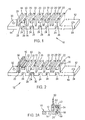
Figure 1 is a perspective view of a comb-like support structure according to the present invention; -
Figure 2 is a perspective view of the comb-like support structure including a barrier and an electrically conductive ring installed in a slot of the comb-like structure; -
Figure 2A is a cross-sectional view of a portion of the comb-like structure including the barrier and electrically conductive ring mounted to the comb-like support structure; -
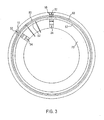
Figure 3 is a top plan view of a pancake type slip ring according to the present invention; -
Figure 4A is a side elevational view of a second embodiment according to the present invention in which each of the slip rings have the same diameter; and -
Figure 4B is a top plan view of the embodiment shown inFigure 4A . - Referring first to
Figure 1 , a perspective view of a comb-like structure 10 is illustrated. As described below, the comb-like structure advantageously eliminates the need for molding the conductive rings as part of the base or plating the conductive rings into completed bases. Further, the present invention eliminates the need to machine an annular base or perform expensive and time consuming operations to roll conductive strips into a machined base member. The comb-like structure 10 has anupper surface 12 and alower surface 14. The electrically non-conductive comb-like structure 10 can be machined or molded from a suitable material. The comb includes a series of relativelynarrow grooves 20 extending from atop surface 16. Although thegrooves 20 appear to terminate at approximately same height asupper surface 12, thegrooves 20 can extend downwardly belowupper surface 12 as depicted inFigure 1 . A series of relativelywider grooves 22 are located betweengrooves 20. As depicted inFigure 1 , there are two adjacent relativelynarrow grooves 20' and 20", the purpose of which will be explained in detail below. - Extending inwardly from the
lower surface 14 are a plurality of relativelywider grooves 24 which are aligned withgrooves 22. A throughhole 26 extends frombottom surface 28 ofgrooves 22 through to eachbottom surface 30 ofgrooves 24. - Turning now to
Figure 2 , the comb-like structure 10 is shown with abarrier 50 and an electricallyconductive slip ring 52 installed inslots barrier 50 andconductive ring 52 are illustrated although eachslot corresponding barrier 50 orconductive ring 52. - UL has standards for voltage creapage paths.
- The high voltage circuits, which could be as high as 500 volts or more, would need multiple barriers to stop arcing from one circuit to another.
- The
barrier 50 and theconductive ring 52 are engaged with thecomb 10, although it should be understood, particularly with reference toFigures 3 and4 , that therings rings grooves - As depicted in
Figure 2A , thebarrier 50 is mounted in theslot 20 by means such as press-fit, epoxy or the like. Thering 52 has a plurality ofstuds 54 which are welded or otherwise affixed to thering 52. Thestud 54 extends through a correspondinghole 26 in the comb-like structure 10. A washer andnut groove 24 and secure the respective section ofring 52 to the comb-like structure 10. As depicted inFigures 2 and 2A , thering 52 is shallower than the correspondingslot 20 such that atop surface 60 of thering 52 is positioned below thetop surface 16 of the comb-like structure 10. By contrast, thebarrier 50 extends upwardly from thetop surface 16. In this manner, brushes (not shown) are kept electrically isolated from adjacent brushes and rings during the rotatable structural member (not shown). - A pancake type embodiment is depicted in
Figure 3 whereas an annular slip ring assembly is depicted inFigures 4A and 4B . InFigure 3 , a plurality of comb-like structure 10 are fastened to a base orbracket 70 throughholes like structure 10, using any type of known fastener. The comb-like structures 10 are circumferentially spaced from each other. The number of combs around the circumference is controlled by the mechanical stiffness of the conductive rings 52. A sufficient number of comb-like structures 10 must be installed on therings 52 to maintain electrical contact as the brush moves over the non-supported area between comb-like structures 10. As depicted inFigure 3 , therings 52 andbarriers 50 are mounted to the comb-like structure 10. Electrical connections are made to each of the rings and the electrical connections exit the comb-like structures 10 to the inner diameter of the slip ring. Theelectrical barriers 50 between theconductive rings 52 can be epoxied or mechanically locked in place. The barriers are manufactured from a suitable, flexible, non-conductive material that can be easily installed in theslots 20 in the comb-like structures 10. The comb-like structures 10, rings 50, 52 can be secured to an epoxy base, either on the face as depicted inFigure 3 or around the circumference as depicted inFigure 4 . As depicted inFigure 3 , each of therings - As depicted in
Figure 4 , the individual comb-like structures 10 are mounted to a base or to individual brackets to support the comb-like structures. As depicted inFigure 4B each of theelectrical rings 52 has the same diameter. In all other respects, theFigure 4 embodiment is identical to theFigure 3 embodiment. - It will be readily seen by one of ordinary skill in the art that the present invention fulfills all of the objects set forth above. It is intended that the protection granted hereon be limited only by the definition contained in the appended claims and equivalents thereof.
Claims (5)
- An electrical slip ring assembly, comprising:a first plurality of annular conductive rings (52) spaced from one another;a second plurality of circularly-spaced electrically-nonconductive support structures (10), each having inwardly-extending slots (20, 22);a third plurality of annular electrically-isolating barriers (50);wherein each of said support structures (10) has a comb-like structure;wherein said slots include ring slots (22) and barrier slots (20), each ring slot (22) having a barrier slot (20) adjacent thereto;wherein said barrier slots (20) extend inwardly into said comb-like structure from the top surface (16) thereof a greater distance than do the adjacent ring slots (22);said conductive rings (52) being mounted in said ring slots (22) and extending outwardly having a top surface (60) that does not extend beyond the top surface (16) of said comb-like structure;said electrically-isolating barriers (50) being mounted in said barrier slots (20) and extending outwardly beyond the top surface (16) of said comb-like structure; andwherein the top surface of each barrier extends outwardly beyond the top surfaces (60) of the adjacent conductive rings.
- An electrical slip ring assembly as set forth in claim 1 wherein said conductive rings (52) are spaced vertically from one another when mounted on said support structures (10).
- An electrical slip ring assembly as set forth in claim 1 wherein said conductive rings (52) are spaced horizontally from one another when mounted on said support structures.
- An electrical slip ring assembly as set forth in claim 1 wherein each of said conductive rings (52) has the same diameter.
- An electrical slip ring assembly as set forth in claim 1 wherein each of said conductive rings (52) has a different diameter.
Applications Claiming Priority (2)
| Application Number | Priority Date | Filing Date | Title |
|---|---|---|---|
| US10/013,535 US6664697B2 (en) | 2001-12-13 | 2001-12-13 | Electrical slip ring apparatus having multiple spaced apart support structures |
| US13535 | 2001-12-13 |
Publications (2)
| Publication Number | Publication Date |
|---|---|
| EP1320154A1 EP1320154A1 (en) | 2003-06-18 |
| EP1320154B1 true EP1320154B1 (en) | 2011-10-26 |
Family
ID=21760452
Family Applications (1)
| Application Number | Title | Priority Date | Filing Date |
|---|---|---|---|
| EP02027207A Expired - Lifetime EP1320154B1 (en) | 2001-12-13 | 2002-12-05 | Electrical slip ring apparatus having multiple spaced apart support structures |
Country Status (4)
| Country | Link |
|---|---|
| US (1) | US6664697B2 (en) |
| EP (1) | EP1320154B1 (en) |
| JP (1) | JP4446328B2 (en) |
| CA (1) | CA2414104C (en) |
Families Citing this family (7)
| Publication number | Priority date | Publication date | Assignee | Title |
|---|---|---|---|---|
| US7105983B2 (en) | 2004-06-18 | 2006-09-12 | Moog Inc. | Electrical contact technology and methodology for the manufacture of large-diameter electrical slip rings |
| US7009323B1 (en) | 2004-12-06 | 2006-03-07 | Siemens Vdo Automotive Inc. | Robust commutator bar anchoring configuration with dove-tailed features |
| US7131844B1 (en) | 2005-12-19 | 2006-11-07 | Insul-8 Corporation | Collector ring assembly |
| US7597565B1 (en) | 2008-03-11 | 2009-10-06 | Textron Systems Corporation | Continuous sliding electrical contact tape |
| US9214777B2 (en) * | 2014-03-24 | 2015-12-15 | Goodrich Corporation | Landing gear electrical swivel |
| EP3217487B1 (en) | 2016-03-08 | 2019-05-08 | Schleifring GmbH | Modular slip ring system |
| ES2866408T3 (en) * | 2018-08-21 | 2021-10-19 | Flender Gmbh | Slip ring bridge, slip ring unit, electric machine and wind turbine |
Citations (3)
| Publication number | Priority date | Publication date | Assignee | Title |
|---|---|---|---|---|
| DE1094867B (en) * | 1955-10-10 | 1960-12-15 | Siemens Schuckertwerke Gmbh | Process for the production of a slip ring body for electrical machines or the like. |
| US4782580A (en) * | 1986-04-30 | 1988-11-08 | National Machine Company, Inc. | Method of manufacture of slip ring assembly |
| US5745976A (en) * | 1996-05-13 | 1998-05-05 | Litton Systems Inc. | Method of manufacturing an electrical slip ring base |
Family Cites Families (5)
| Publication number | Priority date | Publication date | Assignee | Title |
|---|---|---|---|---|
| DE917496C (en) | 1951-10-07 | 1954-09-06 | Pintsch Bamag Ag | Support body for slip rings on electrical equipment |
| US5054189A (en) | 1990-10-25 | 1991-10-08 | Litton Systetms, Inc. | Method of manufacturing an electrical slip ring assembly |
| JPH11505668A (en) * | 1995-03-20 | 1999-05-21 | エムシーエヌシー | Solder bump manufacturing method and structure including titanium barrier layer |
| US5734218A (en) * | 1996-05-13 | 1998-03-31 | Litton Systems, Inc. | Electrical slip ring and method of manufacturing same |
| US6356002B1 (en) * | 1999-02-08 | 2002-03-12 | Northrop Grumman Corporation | Electrical slip ring having a higher circuit density |
-
2001
- 2001-12-13 US US10/013,535 patent/US6664697B2/en not_active Expired - Lifetime
-
2002
- 2002-12-05 EP EP02027207A patent/EP1320154B1/en not_active Expired - Lifetime
- 2002-12-12 CA CA002414104A patent/CA2414104C/en not_active Expired - Fee Related
- 2002-12-13 JP JP2002362817A patent/JP4446328B2/en not_active Expired - Fee Related
Patent Citations (3)
| Publication number | Priority date | Publication date | Assignee | Title |
|---|---|---|---|---|
| DE1094867B (en) * | 1955-10-10 | 1960-12-15 | Siemens Schuckertwerke Gmbh | Process for the production of a slip ring body for electrical machines or the like. |
| US4782580A (en) * | 1986-04-30 | 1988-11-08 | National Machine Company, Inc. | Method of manufacture of slip ring assembly |
| US5745976A (en) * | 1996-05-13 | 1998-05-05 | Litton Systems Inc. | Method of manufacturing an electrical slip ring base |
Also Published As
| Publication number | Publication date |
|---|---|
| CA2414104C (en) | 2009-04-07 |
| EP1320154A1 (en) | 2003-06-18 |
| JP2003204658A (en) | 2003-07-18 |
| US20030111928A1 (en) | 2003-06-19 |
| US6664697B2 (en) | 2003-12-16 |
| JP4446328B2 (en) | 2010-04-07 |
| CA2414104A1 (en) | 2003-06-13 |
Similar Documents
| Publication | Publication Date | Title |
|---|---|---|
| US4559464A (en) | Molded commutator and method of manufacture | |
| EP1320154B1 (en) | Electrical slip ring apparatus having multiple spaced apart support structures | |
| CA1048657A (en) | Gang bonding interconnect tape for semiconductive devices and method of making same | |
| US5734218A (en) | Electrical slip ring and method of manufacturing same | |
| US4684179A (en) | Slip ring assembly for method of making same | |
| KR101687157B1 (en) | Stator system for an electric motor | |
| US5491373A (en) | Commutators | |
| US3861027A (en) | Method of manufacturing a rotor assembly for a dynamo electric machine | |
| CN1247403A (en) | Motor and mfg. method thereof | |
| HK1081330A1 (en) | Commutator for an electrical machine and method for producing the same | |
| KR20150100538A (en) | Apparatus for liquid treatment of wafer shaped articles | |
| US5054189A (en) | Method of manufacturing an electrical slip ring assembly | |
| US6161275A (en) | Method of manufacturing commutators for electric motors | |
| US4638202A (en) | Commutator and method of making same | |
| EP0116582A1 (en) | Rail insulator for the securing of a conductor rail on a rail support. | |
| US3376443A (en) | Commutator and method of making | |
| US4710664A (en) | Space block control means for dynamoelectric machine | |
| US3182217A (en) | Commutating apparatus | |
| WO2004105213A3 (en) | Permanent magnet electric generator | |
| EP3217487B1 (en) | Modular slip ring system | |
| US4890377A (en) | Method of making cummutators | |
| EP0994554B1 (en) | Commutator and method of manufacturing the same | |
| EP1094553A1 (en) | Contact discs for conducting plates of busbars | |
| US20200136482A1 (en) | Modular stator | |
| US5993718A (en) | Molded plastic mounting part |
Legal Events
| Date | Code | Title | Description |
|---|---|---|---|
| PUAI | Public reference made under article 153(3) epc to a published international application that has entered the european phase |
Free format text: ORIGINAL CODE: 0009012 |
|
| AK | Designated contracting states |
Designated state(s): AT BE BG CH CY CZ DE DK EE ES FI FR GB GR IE IT LI LU MC NL PT SE SI SK TR |
|
| AX | Request for extension of the european patent |
Extension state: AL LT LV MK RO |
|
| 17P | Request for examination filed |
Effective date: 20031217 |
|
| AKX | Designation fees paid |
Designated state(s): CH DE GB LI SE |
|
| 17Q | First examination report despatched |
Effective date: 20090810 |
|
| RAP1 | Party data changed (applicant data changed or rights of an application transferred) |
Owner name: MOOG COMPONENTS GROUP INC. |
|
| RAP1 | Party data changed (applicant data changed or rights of an application transferred) |
Owner name: MOOG INC. |
|
| GRAP | Despatch of communication of intention to grant a patent |
Free format text: ORIGINAL CODE: EPIDOSNIGR1 |
|
| GRAJ | Information related to disapproval of communication of intention to grant by the applicant or resumption of examination proceedings by the epo deleted |
Free format text: ORIGINAL CODE: EPIDOSDIGR1 |
|
| GRAP | Despatch of communication of intention to grant a patent |
Free format text: ORIGINAL CODE: EPIDOSNIGR1 |
|
| GRAS | Grant fee paid |
Free format text: ORIGINAL CODE: EPIDOSNIGR3 |
|
| GRAA | (expected) grant |
Free format text: ORIGINAL CODE: 0009210 |
|
| AK | Designated contracting states |
Kind code of ref document: B1 Designated state(s): CH DE GB LI SE |
|
| REG | Reference to a national code |
Ref country code: GB Ref legal event code: FG4D |
|
| REG | Reference to a national code |
Ref country code: CH Ref legal event code: EP |
|
| REG | Reference to a national code |
Ref country code: DE Ref legal event code: R096 Ref document number: 60241392 Country of ref document: DE Effective date: 20111229 |
|
| PG25 | Lapsed in a contracting state [announced via postgrant information from national office to epo] |
Ref country code: SE Free format text: LAPSE BECAUSE OF FAILURE TO SUBMIT A TRANSLATION OF THE DESCRIPTION OR TO PAY THE FEE WITHIN THE PRESCRIBED TIME-LIMIT Effective date: 20111026 |
|
| REG | Reference to a national code |
Ref country code: CH Ref legal event code: PL |
|
| PLBE | No opposition filed within time limit |
Free format text: ORIGINAL CODE: 0009261 |
|
| STAA | Information on the status of an ep patent application or granted ep patent |
Free format text: STATUS: NO OPPOSITION FILED WITHIN TIME LIMIT |
|
| 26N | No opposition filed |
Effective date: 20120727 |
|
| PG25 | Lapsed in a contracting state [announced via postgrant information from national office to epo] |
Ref country code: CH Free format text: LAPSE BECAUSE OF NON-PAYMENT OF DUE FEES Effective date: 20111231 Ref country code: LI Free format text: LAPSE BECAUSE OF NON-PAYMENT OF DUE FEES Effective date: 20111231 |
|
| REG | Reference to a national code |
Ref country code: DE Ref legal event code: R097 Ref document number: 60241392 Country of ref document: DE Effective date: 20120727 |
|
| PGFP | Annual fee paid to national office [announced via postgrant information from national office to epo] |
Ref country code: GB Payment date: 20171227 Year of fee payment: 16 |
|
| PGFP | Annual fee paid to national office [announced via postgrant information from national office to epo] |
Ref country code: DE Payment date: 20171229 Year of fee payment: 16 |
|
| REG | Reference to a national code |
Ref country code: DE Ref legal event code: R119 Ref document number: 60241392 Country of ref document: DE |
|
| GBPC | Gb: european patent ceased through non-payment of renewal fee |
Effective date: 20181205 |
|
| PG25 | Lapsed in a contracting state [announced via postgrant information from national office to epo] |
Ref country code: DE Free format text: LAPSE BECAUSE OF NON-PAYMENT OF DUE FEES Effective date: 20190702 |
|
| PG25 | Lapsed in a contracting state [announced via postgrant information from national office to epo] |
Ref country code: GB Free format text: LAPSE BECAUSE OF NON-PAYMENT OF DUE FEES Effective date: 20181205 |