EP1326203A2 - Method and device for protecting digital circuit parts - Google Patents
Method and device for protecting digital circuit parts Download PDFInfo
- Publication number
- EP1326203A2 EP1326203A2 EP02102850A EP02102850A EP1326203A2 EP 1326203 A2 EP1326203 A2 EP 1326203A2 EP 02102850 A EP02102850 A EP 02102850A EP 02102850 A EP02102850 A EP 02102850A EP 1326203 A2 EP1326203 A2 EP 1326203A2
- Authority
- EP
- European Patent Office
- Prior art keywords
- gate
- inverter
- sensor
- sensors
- output
- Prior art date
- Legal status (The legal status is an assumption and is not a legal conclusion. Google has not performed a legal analysis and makes no representation as to the accuracy of the status listed.)
- Withdrawn
Links
Images
Classifications
-
- H—ELECTRICITY
- H01—ELECTRIC ELEMENTS
- H01L—SEMICONDUCTOR DEVICES NOT COVERED BY CLASS H10
- H01L23/00—Details of semiconductor or other solid state devices
- H01L23/57—Protection from inspection, reverse engineering or tampering
-
- G—PHYSICS
- G06—COMPUTING; CALCULATING OR COUNTING
- G06K—GRAPHICAL DATA READING; PRESENTATION OF DATA; RECORD CARRIERS; HANDLING RECORD CARRIERS
- G06K19/00—Record carriers for use with machines and with at least a part designed to carry digital markings
- G06K19/06—Record carriers for use with machines and with at least a part designed to carry digital markings characterised by the kind of the digital marking, e.g. shape, nature, code
- G06K19/067—Record carriers with conductive marks, printed circuits or semiconductor circuit elements, e.g. credit or identity cards also with resonating or responding marks without active components
- G06K19/07—Record carriers with conductive marks, printed circuits or semiconductor circuit elements, e.g. credit or identity cards also with resonating or responding marks without active components with integrated circuit chips
- G06K19/073—Special arrangements for circuits, e.g. for protecting identification code in memory
- G06K19/07309—Means for preventing undesired reading or writing from or onto record carriers
- G06K19/07372—Means for preventing undesired reading or writing from or onto record carriers by detecting tampering with the circuit
-
- H—ELECTRICITY
- H01—ELECTRIC ELEMENTS
- H01L—SEMICONDUCTOR DEVICES NOT COVERED BY CLASS H10
- H01L2924/00—Indexing scheme for arrangements or methods for connecting or disconnecting semiconductor or solid-state bodies as covered by H01L24/00
- H01L2924/0001—Technical content checked by a classifier
- H01L2924/0002—Not covered by any one of groups H01L24/00, H01L24/00 and H01L2224/00
Definitions
- the invention relates to a method and an arrangement for protecting digital circuit parts, which can be used in particular to store storage units on such digital circuits, in particular smart card controllers, which contain secret data, protect against attacks that follow the approach, digital circuit parts, in particular the digital part of a smart card controller, due to brief voltage drops, e.g. by flashes of light to put them in an undefined state.
- smart cards In a smart card are data storage and arithmetic logic Units integrated in a single chip a few square millimeters in size. Smart cards are used in particular as telephone cards, GSM SIM cards, in the banking sector and used in healthcare. The smart card is thus ubiquitous Computing platform.
- Smart cards are currently primarily used as a safe place to keep secret data and viewed as a secure execution platform for cryptographic algorithms.
- the Assumption of a relatively high security of the data and algorithms on the card lies in the Hardware structure of the card and the external interfaces are justified.
- Critical data such as secret key a public key procedure
- access from outside can even be completely removed.
- a smart card is able to execute algorithms without the Execution of the individual operations can be observed from the outside.
- the algorithms themselves can be protected against changes and readouts on the card.
- object-oriented The smart card can be understood as an abstract data type, the over has a well-defined interface, a specified behavior and even in is able to comply with certain integrity conditions regarding its condition sure.
- Smart cards There are two main types of smart cards. Own memory cards only a serial interface, addressing and security logic and ROM and EEPROM memory. These cards have limited functionality and serve a specific application. But they are particularly cheap to manufacture. As Smart cards made from microprocessor cards are in principle a complete universal computer represents.
- each phase is carried out by a company that specializes in the respective work carried out.
- the semiconductors When manufacturing the semiconductors is especially hard-wired for cards Security logic to pay attention to good internal security. So from the manufacturer a complete final test can be carried out, the complete memory must be free be accessible. The chip is only secured by a transport code after the final test. After that, access to the card memory is only for authorized entities that have the Knowing the transport code, possible. Theft of brand new semiconductors is therefore not an option Consequences.
- Authorized bodies can be personalizers or card issuers. For embedding and printing no further security functions are necessary. The concerned Companies do not need to know the transport code.
- the issuing body e.g. Bank, telephone company, health insurance etc.
- the personal data in the card This process is called personalization. For them, the knowledge of the transport code necessary.
- Chips on chip cards apply to the encryption of this data; a fuse against unauthorized access to the chip is minimal or non-existent; at a Chip card is usually a mechanical access to the data or its extraction chemical removal of the plastic layer with an existing passivation cover of the pierced stylus possible.
- Some hacker attacks also pursue the approach of converting the digital part of a smart card controller into an undefined one Bring condition. Brief voltage drops, e.g. by Flash attacks provoked.
- WO 98/18102 describes a method and an arrangement for protecting electronic ones Computing units described against unwanted access.
- the computing unit is at one or more measuring points the casing determines measured values after at a specified signal feed point signals defined by the computing unit have been applied to the casing.
- a signature is formed from the measured values recorded and in a register stored. Because any injury or damage the special properties of the sheath change, the measured value recorded after an injury results in another Signature as filed in the register for the intact casing. A comparison of the In this case, signatures lead to an error message and further messages for one Case provided steps.
- US 5,465,349 describes a security method for monitoring integrated Circuits to undefined states; first of all, before each data transfer to an external device and secondly before any change (write or delete) from Memory data of the integrated circuit, which is usually in an EPROM or EEPROM are stored, a status query of one or more security registers.
- the Status of the security register is changed if the system has an undefined state detects, for this purpose also sensors, e.g. a sensor which measures the working frequency of the circuit monitored, or an optical sensor can be used can.
- US Pat. No. 6,092,147 describes a distributed check of hardware-independent, executable bytecode described by a computer to a virtual machine is transferred to run there.
- the test is carried out as follows. After the test on the sending computer system has been completed, the test result first confirmed by the virtual machine before the bytecode on the virtual machine is performed.
- protection against unauthorized access to protected memory of an electronic system, in particular of a computer system improved by performing the following steps: setting the Computer system in a mode in which a confirmation process is performed; then a safety circuit is switched into a first one before leaving this operating mode set status; the status of the safety circuit is then checked, the operations performed by the computer system be stopped if the safety circuit is in a different one than that given status.
- the invention is therefore based on the object of a method and an arrangement of the Specify generic type, through which the disadvantages of conventional protective measures be fixed and in particular it is prevented that secret, in one digital circuit part stored data become accessible after it has been possible to bring this digital circuit part into an undefined state.
- An arrangement for protecting digital circuit parts is advantageously constructed in such a way that that the digital circuit part (glue logic) comprises at least one digital sensor 1.
- Another advantage of the method according to the invention is that the voltage drops can be detected within the glue logic.
- this is the invention Process can be used to reduce voltage dips within a smart card controller to detect.
- the Sensors are activated by setting the reset signal to logic zero.
- the senor (s) is (are) designed as a special standard cell, which a NOR gate, an inverter and a capacitor.
- the NOR gate and inverter are connected as a latch.
- the standard cell (s) has a NOR gate and an inverter, the input of the NOR gate with the output of the inverter and a capacitor with the Supply voltage is connected and the input of the inverter to the output of the NOR gate is connected and the reset signal can be applied to the input of the NOR gate and the error signal can be tapped at the output of the NOR gate.
- the threshold voltage in the NOR gate and the transistors used in the inverter are designed differently.
- the sensor (s) is designed as a light or voltage sensor is (are).
- the so-called glue logic is part of a smart card controller.
- a special sensor system distributed over the digital part (glue logic), protects against the above Attacks. Because the sensors are located within the glue logic, the following advantage is obtained. First, the sensors can experience voltage dips there recognize where they are most critical. Second, the sensors are no more than that recognizable.
- the security of the entire chip is significantly increased. Attacks on the glue logic itself, e.g. due to flashes of light, are recognized directly on site.
- the sensors are further very small, which means that a higher number of instances is distributed on the glue logic can be made without losing a lot of chip area.
- the sensors are not recognizable as such or to be distinguished from the standard cells.
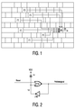
- the digital part according to FIG. 1 is presented below.
- the output signals of standard cells 1 operating as sensors are linked to one another with an OR circuit 2.
- a final output signal 3 of the OR circuit 2 is active when one or more sensors 1 deliver an error signal.
- the exemplary arrangement shown in FIG. 2 of a sensor 1 constructed as a standard cell comprises a NOR gate 1a and an inverter 1b; these work as a latch.
- a node 1d, in which an input of the NOR gate 1a is connected to the output of the inverter 1b, is connected to a supply voltage VDD via a capacitor 1c.
- the input of the inverter 1b is connected to the output of the NOR gate 1a.
- a reset signal can be applied to a further input of NOR gate 1a and the error signal to be supplied by this sensor 1 can be tapped at the output of NOR gate 1a.
- the latch comprising the NOR gate 1a and the inverter 1b can by means of the reset signal be reset so that the error signal emitted by sensor 1 becomes inactive and assumes the state logic "0". In this state, node 1d is logically "1".
Landscapes
- Engineering & Computer Science (AREA)
- Computer Hardware Design (AREA)
- Physics & Mathematics (AREA)
- General Physics & Mathematics (AREA)
- Microelectronics & Electronic Packaging (AREA)
- Computer Security & Cryptography (AREA)
- General Engineering & Computer Science (AREA)
- Theoretical Computer Science (AREA)
- Condensed Matter Physics & Semiconductors (AREA)
- Power Engineering (AREA)
- Storage Device Security (AREA)
- Techniques For Improving Reliability Of Storages (AREA)
Abstract
Description
Die Erfindung betrifft ein Verfahren und eine Anordnung zum Schutz von digitalen Schaltungsteilen, die insbesondere genutzt werden können, um Speichereinheiten auf solchen digitalen Schaltungen, insbesondere Smartcard-Controllern, die geheime Daten enthalten, gegen Attacken zu schützen, die den Ansatz verfolgen, digitale Schaltungsteile, insbesondere den Digitalteil eines Smartcard-Controllers, durch kurzzeitige Spannungseinbrüche, z.B. durch Lichtblitzattacken, in einen undefinierten Zustand zu versetzen.The invention relates to a method and an arrangement for protecting digital circuit parts, which can be used in particular to store storage units on such digital circuits, in particular smart card controllers, which contain secret data, protect against attacks that follow the approach, digital circuit parts, in particular the digital part of a smart card controller, due to brief voltage drops, e.g. by flashes of light to put them in an undefined state.
Die Entwicklung der Mikroelektronik in den 70er Jahren ermöglichte es, kleine Computer im Kreditkartenformat ohne Benutzungsschnittstelle herzustellen. Solche Computer werden als Smartcards bezeichnet. In einer Smartcard sind Datenspeicher und arithmetischlogische Einheiten in einem einzigen Chip von wenigen Quadratmillimetern Größe integriert. Smartcards werden insbesondere als Telefonkarten, GSM-SIM-Karten, im Bankenbereich und im Gesundheitswesen eingesetzt. Die Smartcard ist damit zur allgegenwärtigen Rechenplattform geworden.The development of microelectronics in the 1970s made it possible to use small computers in credit card format without a user interface. Such computers will referred to as smart cards. In a smart card are data storage and arithmetic logic Units integrated in a single chip a few square millimeters in size. Smart cards are used in particular as telephone cards, GSM SIM cards, in the banking sector and used in healthcare. The smart card is thus ubiquitous Computing platform.
Smartcards werden derzeit vornehmlich als sicherer Aufbewahrungsort für geheime Daten und als sichere Ausführungsplattform für kryptographische Algorithmen betrachtet. Die Annahme einer relativ hohen Sicherheit der Daten und Algorithmen auf der Karte liegt im Hardwareaufbau der Karte und den nach außen geführten Schnittstellen begründet. Die Karte stellt sich nach außen als "Black Box" dar, deren Funktionalität nur über eine wohldefinierte Hardware- und Softwareschnittstelle in Anspruch genommen werden kann und die bestimmte Sicherheitspolicies erzwingen kann. Zum einen kann der Zugriff auf Daten an bestimmte Bedingungen geknüpft werden. Kritische Daten, wie z.B. geheime Schlüssel eines Public-Key-Verfahrens, können dem Zugriff von außen sogar völlig entzogen werden. Zum anderen ist eine Smartcard in der Lage, Algorithmen auszuführen, ohne dass die Ausführung der einzelnen Operationen von außen beobachtet werden kann. Die Algorithmen selbst können auf der Karte vor Veränderung und Auslesen geschützt werden. Im objektorientierten Sinn läßt sich die Smartcard als abstrakter Datentyp auffassen, der über eine wohldefinierte Schnittstelle verfügt, ein spezifiziertes Verhalten aufweist und selbst in der Lage ist, die Einhaltung bestimmter Integritätsbedingungen bezüglich seines Zustandes sicherzustellen.Smart cards are currently primarily used as a safe place to keep secret data and viewed as a secure execution platform for cryptographic algorithms. The Assumption of a relatively high security of the data and algorithms on the card lies in the Hardware structure of the card and the external interfaces are justified. The Outwardly, the card presents itself as a "black box", the functionality of which is only possible via a well-defined one Hardware and software interface can be used and that can enforce certain security policies. Firstly, access to data subject to certain conditions. Critical data, such as secret key a public key procedure, access from outside can even be completely removed. On the other hand, a smart card is able to execute algorithms without the Execution of the individual operations can be observed from the outside. The algorithms themselves can be protected against changes and readouts on the card. In object-oriented The smart card can be understood as an abstract data type, the over has a well-defined interface, a specified behavior and even in is able to comply with certain integrity conditions regarding its condition sure.
Es gibt im Wesentlichen zwei verschiedene Typen von Smartcards. Speicherkarten besitzen lediglich eine serielle Schnittstelle, eine Adressierungs- und Sicherheitslogik und ROMund EEPROM-Speicher. Diese Karten besitzen nur eingeschränkte Funktionalität und dienen einer spezifischen Anwendung. Dafür sind sie besonders billig herzustellen. Als Mikroprozessorkarten hergestellte Smartcards stellen im Prinzip einen vollständigen Universalrechner dar.There are two main types of smart cards. Own memory cards only a serial interface, addressing and security logic and ROM and EEPROM memory. These cards have limited functionality and serve a specific application. But they are particularly cheap to manufacture. As Smart cards made from microprocessor cards are in principle a complete universal computer represents.
Der Herstellungs- und Auslieferungsprozeß für Chipkarten gliedert sich in folgende Phasen:
- Herstellen des Halbleiters,
- Einbetten des Halbleiters,
- Bedrucken der Karte,
- Personalisierung der Karte,
- Ausgeben der Karte.
- Manufacturing the semiconductor,
- Embedding the semiconductor,
- Printing on the card,
- Personalization of the card,
- Issue the card.
Im Allgemeinen wird jede Phase von einer auf die jeweilige Arbeit spezialisierten Firma durchgeführt. Beim Herstellen der Halbleiter ist insbesondere bei Karten mit fest verdrahteter Sicherheitslogik auf eine gute betriebsinterne Sicherheit zu achten. Damit vom Hersteller ein korrekter Endtest durchgeführt werden kann, muß der komplette Speicher frei zugänglich sein. Erst nach dem Endtest wird der Chip durch einen Transportcode gesichert. Danach ist der Zugriff auf den Kartenspeicher nur für berechtigte Stellen, die den Transportcode kennen, möglich. Ein Diebstahl fabrikneuer Halbleiter bleibt damit ohne Folgen. Berechtigte Stellen können Personalisierer bzw. Kartenausgeber sein. Für das Einbetten und Bedrucken sind keine weiteren Sicherungsfunktionen notwendig. Die betreffenden Firmen brauchen den Transportcode nicht zu kennen. In general, each phase is carried out by a company that specializes in the respective work carried out. When manufacturing the semiconductors is especially hard-wired for cards Security logic to pay attention to good internal security. So from the manufacturer a complete final test can be carried out, the complete memory must be free be accessible. The chip is only secured by a transport code after the final test. After that, access to the card memory is only for authorized entities that have the Knowing the transport code, possible. Theft of brand new semiconductors is therefore not an option Consequences. Authorized bodies can be personalizers or card issuers. For embedding and printing no further security functions are necessary. The concerned Companies do not need to know the transport code.
Im Allgemeinen überträgt nicht der Kartenhersteller, sondern die ausgebende Stelle (z.B. Bank, Telefongesellschaft, Krankenkasse etc.) die personenspezifischen Daten in die Karte. Diesen Vorgang nennt man Personalisierung. Für sie ist die Kenntnis des Transportcodes notwendig.In general, it is not the card manufacturer that transfers, but the issuing body (e.g. Bank, telephone company, health insurance etc.) the personal data in the card. This process is called personalization. For them, the knowledge of the transport code necessary.
Das Ausgeben der Karte, also der Transport von der ausgebenden Stelle zum Karteninhaber, stellt ein weiteres Sicherheitsproblem dar. Genau genommen ist nur die persönliche Ausgabe an den Karteninhaber gegen Unterschrift und Vorlage des Personalausweises sicher. Ein Versand per Post ist zwar oft wirtschaftlicher, aber auch ziemlich unsicher. Ein Problem ist auch das Übermitteln der PIN an den Karteninhaber, hier muß die gleiche Sorgfalt wie für die Karte gelten.Issuing the card, i.e. the transport from the issuing point to the card holder, is another security problem. Strictly speaking, only personal Issue to the cardholder securely upon signature and presentation of the identity card. Sending by post is often more economical, but also rather unsafe. On Another problem is the transmission of the PIN to the cardholder, the same must be the case here Care as for the card.
Bedingt durch die brisanten, sicherheitsrelevanten Inhalte der auf Smartcard-Controllern befindlichen Speicher ist neben der Beachtung dieser Sicherungsmaßnahmen ein zusätzlicher Schutz gegen mögliche Aktivitäten von Hackern zu gewährleisten, die sich auf alle Phasen des Lebenslaufes einer Smartcard - beginnend von der Herstellung, über Transport, Nutzung der Karte bis zu Manipulationen unbrauchbar gewordener Karten - erstrecken.Due to the explosive, security-relevant content of the smart card controllers existing storage is an additional to the observance of these security measures Ensure protection against possible activities by hackers that affect everyone Phases of the life cycle of a smart card - starting with the production, through transport, Use of the card to manipulate cards that have become unusable - extend.
Das größte Augenmerk beim Schutz gegen ein Ausspähen von Daten und Programmen auf Datenträgern, z.B. Chips auf Chipkarten, gilt der Verschlüsselung dieser Daten; eine Sicherung gegen unerlaubten Zugriff zum Chip ist minimal oder nicht gegeben; bei einer Chipkarte ist ein mechanischer Zugriff auf die Daten bzw. deren Entnahme meist nach chemischer Entfernung der Kunststoffschicht mit einer durch eine vorhandene Passivierungsabdeckung des Chips durchgestochenen Tastnadel möglich. Einige Hacker-Attacken verfolgen auch den Ansatz, den Digitalteil eines Smartcard-Controllers in einen undefinierten Zustand zu bringen. Hierbei werden kurzzeitige Spannungseinbrüche z.B. durch Lichtblitzattacken provoziert.The greatest attention in protecting against spying on data and programs Data carriers, e.g. Chips on chip cards apply to the encryption of this data; a fuse against unauthorized access to the chip is minimal or non-existent; at a Chip card is usually a mechanical access to the data or its extraction chemical removal of the plastic layer with an existing passivation cover of the pierced stylus possible. Some hacker attacks also pursue the approach of converting the digital part of a smart card controller into an undefined one Bring condition. Brief voltage drops, e.g. by Flash attacks provoked.
In der WO 98/18102 ist ein Verfahren und eine Anordnung zum Schutz von elektronischen Recheneinheiten gegen unerwünschten Zugriff beschrieben. Dabei wird die einem Angriff ausgesetzte Seite der Recheneinheit mit einer Ummantelung mit inhomogenen Eigenschaften versehen. Von der Recheneinheit werden an einer oder mehreren Meßstellen der Ummantelung Meßwerte ermittelt, nachdem an einer festgelegten Signalaufgabestelle der Ummantelung von der Recheneinheit definierte Signale angelegt wurden. Mit den dabei aufgenommenen Meßwerten wird eine Signatur gebildet und in einem Register abgelegt. Da jede Verletzung bzw. Beschädigung die speziellen Eigenschaften der Ummantelung verändern, ergibt der nach einer Verletzung aufgenommene Meßwert eine andere Signatur, als im Register für die unversehrte Ummantelung abgelegt ist. Ein Vergleich der Signaturen führt in diesem Fall zu einer Fehlermeldung und zu weiteren für einen solchen Fall vorgesehenen Schritten.WO 98/18102 describes a method and an arrangement for protecting electronic ones Computing units described against unwanted access. The one Attack exposed side of the computing unit with a casing with inhomogeneous Provide properties. The computing unit is at one or more measuring points the casing determines measured values after at a specified signal feed point signals defined by the computing unit have been applied to the casing. With A signature is formed from the measured values recorded and in a register stored. Because any injury or damage the special properties of the sheath change, the measured value recorded after an injury results in another Signature as filed in the register for the intact casing. A comparison of the In this case, signatures lead to an error message and further messages for one Case provided steps.
Eine Methode, um unbefugtes Ausführen von sicherheitsrelevanten Programmen, z.B. in Smartcards, zu verhindern, wird in der US-Patentschrift 5,682,031 beschrieben. Bei Anwendung der Methode werden von einem in den EPROM der Smartcard eingeschriebenen logischen Riegel (lock) mehrere Kopien erzeugt, welche an unterschiedlichen Speicherorten im EPROM abgelegt und durch eine ODER-Logik verknüpft werden. Eine Sicherung nach dieser Methode verhindert zwar die unbefugte Ausführung der so geschützten sicherheitsrelevanten Programme, wenn sie blockiert werden. Allerdings wird damit nicht garantiert, dass dieser Schutz wirksam ist, wenn sich der Smartcard-Controller in einem undefinierten Zustand befindet.A method to prevent unauthorized execution of security-relevant programs, e.g. in Preventing smart cards is described in U.S. Patent No. 5,682,031. When using The method are written in the EPROM of the smart card logical lock (lock) creates multiple copies, which are in different locations stored in the EPROM and linked by an OR logic. A backup According to this method, the unauthorized execution of the protected security-related products is prevented Programs if they are blocked. However, this does not guarantee that this protection is effective if the smart card controller is in an undefined Condition.
Die US 5,465,349 beschreibt ein Sicherungsverfahren zur Überwachung von integrierten Schaltkreisen auf undefinierte Zustände; dazu erfolgt erstens vor jeder Datenübertragung an ein externes Gerät und zweitens vor jeder Änderung (Schreiben bzw. Löschen) von Speicherdaten des integrierten Schaltkreises, die in der Regel in einem EPROM oder EEPROM abgelegt sind, eine Statusabfrage eines oder mehrerer Sicherheitsregister. Der Status der Sicherheitsregister wird verändert, wenn das System einen nicht definierten Zustand feststellt, wobei zu diesem Zweck auch Sensoren, z.B. ein Sensor, welcher die Arbeitsfrequenz des Schaltkreises überwacht, oder ein optischer Sensor, eingesetzt werden können.US 5,465,349 describes a security method for monitoring integrated Circuits to undefined states; first of all, before each data transfer to an external device and secondly before any change (write or delete) from Memory data of the integrated circuit, which is usually in an EPROM or EEPROM are stored, a status query of one or more security registers. The Status of the security register is changed if the system has an undefined state detects, for this purpose also sensors, e.g. a sensor which measures the working frequency of the circuit monitored, or an optical sensor can be used can.
In der US-Patentschrift US 6,092,147 wird eine verteilte Überprüfung von hardwareunabhängigem, ausführbarem Bytecode beschrieben, der von einer Rechenanlage an eine virtuelle Maschine übertragen wird, um dort ausgeführt zu werden. Bei der Prüfung wird der Bytecode mit vorgegebenen Kriterien verglichen; dabei erfolgt die Prüfung folgenderweise. Nach abgeschlossener Prüfung auf der sendenden Rechenanlage wird das Prüfergebnis von der virtuellen Maschine erst bestätigt, bevor der Bytecode auf der virtuellen Maschine ausgeführt wird.US Pat. No. 6,092,147 describes a distributed check of hardware-independent, executable bytecode described by a computer to a virtual machine is transferred to run there. When examining comparing the bytecode with specified criteria; the test is carried out as follows. After the test on the sending computer system has been completed, the test result first confirmed by the virtual machine before the bytecode on the virtual machine is performed.
Mit einer in der US-Patentschrift 6,249,872 angegebenen Methode wird der Schutz gegen unerlaubten Zugriff auf geschützte Speicher eines elektronischen Systems, insbesondere eines Computersystems, verbessert, indem folgende Schritte ausgeführt werden: Setzen des Computersystems in eine Betriebsart, in der ein Bestätigungsprozeß durchgeführt wird; anschließend wird vor Verlassen dieser Betriebsart ein Sicherheits-Schaltkreis in einen ersten vorgegebenen Status versetzt; anschließend erfolgt eine Prüfung des Status des Sicherheits-Schaltkreises, wobei die von dem Computersystem ausgeführten Operationen gestoppt werden, wenn sich der Sicherheits-Schaltkreis in einem anderen als dem vorgegebenen Status befindet.With a method specified in US Pat. No. 6,249,872, protection against unauthorized access to protected memory of an electronic system, in particular of a computer system, improved by performing the following steps: setting the Computer system in a mode in which a confirmation process is performed; then a safety circuit is switched into a first one before leaving this operating mode set status; the status of the safety circuit is then checked, the operations performed by the computer system be stopped if the safety circuit is in a different one than that given status.
Die sich auf Smartcard-Controllern befindende Sensorik basiert üblicherweise aufAnalogschaltungstechnik. Diese analog ausgeführten Schaltungsteile (z.B. Spannungs-, Licht-, Temperatur- und Lichtsensoren) müssen heute von der sog. Glue-Logic getrennt gehalten werden. Die Gründe dafür sind:
- Störungsempfindlichkeit ― Eng benachbarte digitale Schaltungsteile stören die empfindliche Sensorik.
- Schaltungselemente ― In analogen Schaltungen werden nicht nur die NMOS- und PMOS-Standardtransistoren verwendet, sondern auch speziell dimensionierte Transistoren, Kondensatoren und Widerstände. Diese passen aufgrund ihrer Größe nicht in das vorgegebene Raster der Standardzellen.
- Interference sensitivity - Closely adjacent digital circuit parts interfere with the sensitive sensors.
- Circuit elements - In analog circuits not only the NMOS and PMOS standard transistors are used, but also specially dimensioned transistors, capacitors and resistors. Due to their size, these do not fit into the specified grid of standard cells.
Die Folge davon ist, dass Spezialisten die Sensorik lokalisieren können. Darüber hinaus ist es mit speziellen Geräten (z.B. mit Focus Ion Beam, FIB) möglich, die bereits lokalisierte Sensorik auszuschalten.The consequence of this is that specialists can localize the sensors. Beyond that it is possible with special devices (e.g. with Focus Ion Beam, FIB) that have already been localized Switch off sensors.
Natürlich können sensible Schaltungsteile mittels speziellem Layout geschützt werden, dies bedeutet aber einen hohen Aufwand, der heute bei Smartcard-Controllern üblich ist. Zum Teil kann ein erfahrener Hacker trotzdem Manipulationen vornehmen. Of course, sensitive circuit parts can be protected using a special layout, this but means a lot of effort, which is common today with smart card controllers. To the Some experienced hackers can still perform manipulations.
Der Erfindung liegt deshalb die Aufgabe zugrunde, ein Verfahren und eine Anordnung der gattungsgemäßen Art anzugeben, durch welche die Nachteile der herkömmlichen Schutzmaßnamen behoben werden und insbesondere verhindert wird, dass geheime, in einem digitalen Schaltungsteil gespeicherte Daten zugänglich werden, nachdem es gelungen ist, diesen digitalen Schaltungsteil in einen undefinierten Zustand zu bringen.The invention is therefore based on the object of a method and an arrangement of the Specify generic type, through which the disadvantages of conventional protective measures be fixed and in particular it is prevented that secret, in one digital circuit part stored data become accessible after it has been possible to bring this digital circuit part into an undefined state.
Erfindungsgemäß wird diese Aufgabe gelöst durch die Merkmale im kennzeichnenden Teil
der Ansprüche 1 und 6 im Zusammenwirken mit den Merkmalen im Oberbegriff. Zweckmäßige
Ausgestaltungen der Erfindung sind in den Unteransprüchen enthalten.According to the invention, this object is achieved by the features in the characterizing part
of
Ein besonderer Vorteil des Verfahrens zum Schutz von digitalen Schaltungsteilen besteht darin, dass Spannungseinbrüche detektiert werden.There is a particular advantage of the method for protecting digital circuit parts in that voltage dips are detected.
Eine Anordnung zum Schutz von digitalen Schaltungsteilen ist vorteilhaft so aufgebaut,
dass der digitale Schaltungsteil (Glue-Logic) mindestens einen digitalen Sensor 1 umfaßt.An arrangement for protecting digital circuit parts is advantageously constructed in such a way that
that the digital circuit part (glue logic) comprises at least one
Ein weiterer Vorteil des erfindungsgemäßen Verfahrens besteht darin, dass die Spannungseinbrüche innerhalb der Glue-Logic detektiert werden. Insbesondere ist das erfindungsgemäße Verfahren einsetzbar, um Spannungseinbrüche innerhalb eines Smartcard-Controllers zu detektieren.Another advantage of the method according to the invention is that the voltage drops can be detected within the glue logic. In particular, this is the invention Process can be used to reduce voltage dips within a smart card controller to detect.
In einer weiteren bevorzugter Anwendung des erfindungsgemäßen Verfahrens ist vorgesehen, dass die Spannungseinbrüche durch digitale Sensoren detektiert werden.In a further preferred application of the method according to the invention, that the voltage dips are detected by digital sensors.
Als vorteilhaft erweist es sich außerdem, wenn bei dem erfindungsgemäßen Verfahren, die Sensoren aktiviert werden, indem das Reset-Signal auf logisch Null gesetzt wird.It also proves to be advantageous if, in the method according to the invention, the Sensors are activated by setting the reset signal to logic zero.
In bevorzugter Ausführung der erfindungsgemäßen Anordnung ist vorgesehen, dass beim Vorhandensein mehrerer Sensoren diese mit einer ODER-Schaltung verknüpft sind.In a preferred embodiment of the arrangement according to the invention it is provided that the The presence of several sensors which are linked with an OR circuit.
Eine weitere bevorzugter Ausführung der erfindungsgemäßen Anordnung ist dadurch ausgezeichnet, dass der (die) Sensor(en) als spezielle Standardzelle ausgebildet ist (sind), welche ein NOR-Gatter, einen Inverter und einen Kondensator umfaßt. Another preferred embodiment of the arrangement according to the invention is distinguished by that the sensor (s) is (are) designed as a special standard cell, which a NOR gate, an inverter and a capacitor.
Vorteilhaft ist es auch, dass NOR-Gatter und Inverter als Latch geschaltet sind. Darüber hinaus ist in bevorzugter Ausgestaltung der Erfindung vorgesehen, dass die Standardzelle(n) ein NOR-Gatter sowie einen Inverter aufweist (aufweisen), wobei der Eingang des NOR-Gatters mit dem Ausgang des Inverters sowie über einen Kondensator mit der Versorgungsspannung verbunden ist und der Eingang des Inverters mit dem Ausgang des NOR-Gatters verbunden ist und am Eingang des NOR-Gatters das Reset-Signal anlegbar und am Ausgang des NOR-Gatters das Fehlersignal abgreifbar ist.It is also advantageous that the NOR gate and inverter are connected as a latch. About that In a preferred embodiment of the invention, it is also provided that the standard cell (s) has a NOR gate and an inverter, the input of the NOR gate with the output of the inverter and a capacitor with the Supply voltage is connected and the input of the inverter to the output of the NOR gate is connected and the reset signal can be applied to the input of the NOR gate and the error signal can be tapped at the output of the NOR gate.
Ebenso erweist es sich als Vorteil, dass die Schwellenspannung der in dem NOR-Gatter und dem Inverter verwendeten Transistoren unterschiedlich ausgelegt sind. Ein weiterer Vorteil besteht darin, dass der (die) Sensor(en) als Licht- oder Spannungssensor ausgebildet ist (sind). In einer bevorzugten Ausgestaltung der erfindungsgemäßen Anordnung ist vorgesehen, dass die sog. Glue-Logic Bestandteil eines Smartcard-Controllers ist.It also proves to be an advantage that the threshold voltage in the NOR gate and the transistors used in the inverter are designed differently. Another The advantage is that the sensor (s) is designed as a light or voltage sensor is (are). In a preferred embodiment of the arrangement according to the invention, that the so-called glue logic is part of a smart card controller.
Eine spezielle Sensorik, über den Digitalteil (Glue-Logic) verteilt, schützt gegen die genannten Attacken. Dadurch, dass sich die Sensoren innerhalb der Glue-Logic befinden, wird folgender Vorteil erlangt. Die Sensoren können erstens Spannungseinbrüche dort erkennen, wo sie am kritischsten sind. Zweitens sind die Sensoren nicht mehr als solche erkennbar.A special sensor system, distributed over the digital part (glue logic), protects against the above Attacks. Because the sensors are located within the glue logic, the following advantage is obtained. First, the sensors can experience voltage dips there recognize where they are most critical. Second, the sensors are no more than that recognizable.
Die Sicherheit des gesamten Chips wird deutlich erhöht. Attacken auf die Glue-Logic selbst, z.B. durch Lichtblitzattacken, werden direkt vor Ort erkannt. Weiter sind die Sensoren sehr klein, wodurch eine höhere Anzahl von Instanzen auf der Glue-logic verteilt werden kann, ohne viel Chipfläche zu verlieren. Die Sensoren sind als solche nicht erkennbar oder von den Standardzellen zu unterscheiden.The security of the entire chip is significantly increased. Attacks on the glue logic itself, e.g. due to flashes of light, are recognized directly on site. The sensors are further very small, which means that a higher number of instances is distributed on the glue logic can be made without losing a lot of chip area. The sensors are not recognizable as such or to be distinguished from the standard cells.
Die Erfindung wird nachfolgend in einem Ausführungsbeispiel anhand der zugehörigen Zeichnungen näher erläutert. Es zeigen:
- Fig. 1
- eine Verteilung der speziellen Standardzellen als Sensoren in einem Digitalteil,
- Fig. 2
- einen Aufbau eines als Standardzelle aufgebauten Sensors.
- Fig. 1
- a distribution of the special standard cells as sensors in a digital part,
- Fig. 2
- a structure of a sensor constructed as a standard cell.
Im Folgenden wird der Digitalteil nach Fig. 1 vorgestellt. Die Ausgangssignale als Sensor
arbeitender Standardzellen 1 werden mit einer ODER-Schaltung 2 miteinander verknüpft.
Ein endgültiges Ausgangssignal 3 der ODER-Schaltung 2 ist dann aktiv, wenn einer oder
mehrere Sensoren 1 ein Fehlersignal liefern.
Die in Fig. 2 gezeigte, beispielhafte Anordnung eines als Standardzelle aufgebauten Sensors
1 umfaßt ein NOR-Gatter 1a und einen Inverter 1b; diese arbeiten als Latch. Ein Knoten
1d, in dem ein Eingang des NOR-Gatters 1a mit dem Ausgang des Inverters 1b verbunden
ist, ist über einen Kondensator 1c mit einer Versorgungsspannung VDD verbunden. Der
Eingang des Inverters 1b ist mit dem Ausgang des NOR-Gatters 1a verbunden. An einem
weiteren Eingang des NOR-Gatters 1a ist ein Reset-Signal anlegbar und am Ausgang des
NOR-Gatters 1a ist das von diesem Sensor 1 zu liefernde Fehlersignal abgreifbar.The digital part according to FIG. 1 is presented below. The output signals of
The exemplary arrangement shown in FIG. 2 of a
Das das NOR-Gatter 1a und den Inverter 1b umfassende Latch kann mittels des Reset-Signals
so zurückgesetzt werden, dass das vom Sensor 1 abgegebene Fehlersignal inaktiv wird
und den Zustand logisch "0" annimmt. Der Knoten 1d ist in diesem Zustand logisch "1".The latch comprising the NOR
Sobald das Reset-Signal auf logisch "0" wechselt, ist der Sensor 1 "scharf". Spannungseinbrüche
an der Versorgungsspannung VDD passieren den Kondensator 1c, so dass am Knoten
1d ein kurzer Spannungseinbruch ankommt. Aufgrund einer speziellen Eigenschaft des
Latches, bestehend aus 1a und 1b, führt dieser Spannungseinbruch zum Kippen des Latches,
das Fehlersignal wechselt auf logisch "1". Dieser Zustand bleibt bis zum nächsten Reset-Puls
gespeichert.As soon as the reset signal changes to logic "0",
Die oben genannte spezielle Eigenschaft ist z.B. durch Asymmetrie gegeben, indem man
die Schwellenspannungen der in den Gattern 1a und 1b verwendeten Transistoren unterschiedlich
auslegt. Hierdurch erhält das Latch eine Vorzugsrichtung, die dem Fehlerzustand
entspricht.The above special property is e.g. given by asymmetry by
the threshold voltages of the transistors used in
Die Erfindung ist nicht beschränkt auf die hier dargestellten Ausführungsbeispiele. Vielmehr ist es möglich, durch Kombination und Modifikation der genannten Mittel und Merkmale weitere Ausführungsvarianten zu realisieren, ohne den Rahmen der Erfindung zu verlassen. The invention is not restricted to the exemplary embodiments shown here. Much more it is possible to combine and modify the means and Features to implement further variants without the scope of the invention to leave.
- 11
- als Sensor arbeitende StandardzelleStandard cell working as a sensor
- 1a1a
- NOR-GatterNOR gate
- 1b1b
- Inverterinverter
- 1c1c
- Kondensatorcapacitor
- 1d1d
- Knotennode
- 22
- ODER-SchaltungOR circuit
- 33
- Ausgangssignaloutput
Claims (13)
dadurch gekennzeichnet, dass Spannungseinbrüche detektiert werden.Process for protecting digital circuit parts,
characterized in that voltage dips are detected.
dadurch gekennzeichnet, dass die Spannungseinbrüche innerhalb wenigstens eines der (als "Glue-Logic" bezeichneten) digitalen Schaltungsteile detektiert werden.Method according to claim 1,
characterized in that the voltage dips are detected within at least one of the digital circuit parts (referred to as "glue logic").
dadurch gekennzeichnet, dass die Spannungseinbrüche innerhalb eines Smartcard-Controllers detektiert werden.Method according to one of the preceding claims,
characterized in that the voltage dips are detected within a smart card controller.
dadurch gekennzeichnet, dass die Spannungseinbrüche durch digitale Sensoren detektiert werden.Method according to one of the preceding claims,
characterized in that the voltage dips are detected by digital sensors.
dadurch gekennzeichnet, dass die Sensoren aktiviert werden, indem das Reset-Signal auf logisch Null gesetzt wird.Method according to one of the preceding claims,
characterized in that the sensors are activated by setting the reset signal to logic zero.
dadurch gekennzeichnet, dass der digitale Schaltungsteil (Glue-Logic) mindestens einen digitalen Sensor (1) umfaßt. Arrangement for the protection of digital circuit parts
characterized in that the digital circuit part (glue logic) comprises at least one digital sensor (1).
dadurch gekennzeichnet, dass beim Vorhandensein mehrerer Sensoren (1) diese mit einer ODER-Schaltung (2) verknüpft sind.Arrangement according to claim 6,
characterized in that in the presence of several sensors (1) these are linked with an OR circuit (2).
dadurch gekennzeichnet, dass der (die) Sensor(en) (1) als spezielle Standardzelle ausgebildet ist (sind), welche ein NOR-Gatter (1a), einen Inverter (1b) und einen Kondensator (1c) umfaßt.Arrangement according to one of claims 6 or 7,
characterized in that the sensor (s) (1) is (are) designed as a special standard cell which comprises a NOR gate (1a), an inverter (1b) and a capacitor (1c).
dadurch gekennzeichnet, dass NOR-Gatter (1a) und Inverter (1b) als Latch geschaltet sind.Arrangement according to claim 8,
characterized in that the NOR gate (1a) and inverter (1b) are connected as a latch.
dadurch gekennzeichnet, dass die Standardzelle(n) (1) ein NOR-Gatter (1a) sowie einen Inverter (1b) aufweist (aufweisen), wobei ein Eingang des NOR-Gatters (1a) mit dem Ausgang des Inverters (1b) sowie über einen Kondensator (1c) mit einer Versorgungsspannung (VDD) verbunden ist und der Eingang des Inverters (1b) mit dem Ausgang des NOR-Gatters (1a) verbunden ist und an einem weiteren Eingang des NOR-Gatters (1a) das Reset-Signal anlegbar und am Ausgang des NOR-Gatters (1a) ein Fehlersignal abgreifbar ist.Arrangement according to claim 8,
characterized in that the standard cell (s) (1) has a NOR gate (1a) and an inverter (1b), an input of the NOR gate (1a) with the output of the inverter (1b) and via a capacitor (1c) is connected to a supply voltage (VDD) and the input of the inverter (1b) is connected to the output of the NOR gate (1a) and the reset signal can be applied to a further input of the NOR gate (1a) and an error signal can be tapped at the output of the NOR gate (1a).
dadurch gekennzeichnet, dass Schwellenspannungen im NOR-Gatter (1a) und im Inverter (1b) verwendeter Transistoren unterschiedlich ausgelegt sind.Arrangement according to one of claims 8 to 10,
characterized in that threshold voltages in the NOR gate (1a) and in the inverter (1b) of transistors used are designed differently.
dadurch gekennzeichnet, dass der (die) Sensor(en) (1) als Licht- oder Spannungssensor ausgebildet ist (sind). Arrangement according to one of claims 6 to 11,
characterized in that the sensor (s) (1) is (are) designed as a light or voltage sensor.
dadurch gekennzeichnet, dass die "Glue-Logic" Bestandteil eines Smartcard-Controllers ist.Arrangement according to one of claims 6 to 12,
characterized in that the "glue logic" is part of a smart card controller.
Applications Claiming Priority (2)
| Application Number | Priority Date | Filing Date | Title |
|---|---|---|---|
| DE10164419A DE10164419A1 (en) | 2001-12-29 | 2001-12-29 | Method and arrangement for protecting digital circuit parts |
| DE10164419 | 2001-12-29 |
Publications (2)
| Publication Number | Publication Date |
|---|---|
| EP1326203A2 true EP1326203A2 (en) | 2003-07-09 |
| EP1326203A3 EP1326203A3 (en) | 2003-10-01 |
Family
ID=7711111
Family Applications (1)
| Application Number | Title | Priority Date | Filing Date |
|---|---|---|---|
| EP02102850A Withdrawn EP1326203A3 (en) | 2001-12-29 | 2002-12-20 | Method and device for protecting digital circuit parts |
Country Status (5)
| Country | Link |
|---|---|
| US (1) | US20030133241A1 (en) |
| EP (1) | EP1326203A3 (en) |
| JP (1) | JP2003233790A (en) |
| CN (1) | CN1430153A (en) |
| DE (1) | DE10164419A1 (en) |
Cited By (1)
| Publication number | Priority date | Publication date | Assignee | Title |
|---|---|---|---|---|
| DE102007059923B4 (en) | 2006-12-06 | 2022-03-17 | Samsung Electronics Co., Ltd. | smart card |
Families Citing this family (7)
| Publication number | Priority date | Publication date | Assignee | Title |
|---|---|---|---|---|
| KR100884566B1 (en) * | 2006-11-16 | 2009-02-19 | 삼성전자주식회사 | Smart card having laser attack detector |
| IL199272A0 (en) * | 2009-06-10 | 2012-07-16 | Nds Ltd | Protection of secret value using hardware instability |
| FR2958078B1 (en) * | 2010-03-24 | 2012-04-20 | St Microelectronics Rousset | METHOD AND DEVICE FOR COUNTERVATING AGAINST ERROR INJECTION ATTACK IN AN ELECTRONIC MICROCIRCUIT |
| EP2369622B1 (en) * | 2010-03-24 | 2015-10-14 | STMicroelectronics Rousset SAS | Method and device of coutermeasure against a fault-injection error attack within an electronic microcircuit |
| EP2541599A1 (en) * | 2011-06-28 | 2013-01-02 | Nxp B.V. | Security semiconductor product |
| CN114968651A (en) * | 2016-06-24 | 2022-08-30 | 国民技术股份有限公司 | System with attack protection architecture |
| CN111460747B (en) * | 2020-04-10 | 2023-03-31 | 重庆百瑞互联电子技术有限公司 | Standard unit tracking method for integrated circuit design |
Citations (5)
| Publication number | Priority date | Publication date | Assignee | Title |
|---|---|---|---|---|
| US4952796A (en) * | 1987-08-31 | 1990-08-28 | SGS-Thomson Microeleronics SA | Light detection circuit having a junction reverse-biased by a current generator |
| US5060261A (en) * | 1989-07-13 | 1991-10-22 | Gemplus Card International | Microcircuit card protected against intrusion |
| DE19601390A1 (en) * | 1996-01-16 | 1997-07-17 | Siemens Ag | Microchip with a completely or partially surrounding opaque casing section |
| US5935223A (en) * | 1996-05-21 | 1999-08-10 | Texas Instruments Incorporated | System for blocking access to a computer device using a glue logic circuit operable to force a target computer device to perform a target abort |
| US6232591B1 (en) * | 1996-11-21 | 2001-05-15 | Atmel Research | Light detection device |
Family Cites Families (7)
| Publication number | Priority date | Publication date | Assignee | Title |
|---|---|---|---|---|
| FR2668274B1 (en) * | 1990-10-19 | 1992-12-31 | Gemplus Card Int | INTEGRATED CIRCUIT WITH IMPROVED ACCESS SECURITY. |
| FR2676294B1 (en) * | 1991-05-06 | 1993-07-16 | Gemplus Card Int | LOCKING METHOD FOR MEMORY CARD. |
| US5835594A (en) * | 1996-02-09 | 1998-11-10 | Intel Corporation | Methods and apparatus for preventing unauthorized write access to a protected non-volatile storage |
| US5847587A (en) * | 1997-01-07 | 1998-12-08 | Holtek Microelectronics Inc. | Means for instantaneously detecting abnormal voltage in a micro controller |
| US6092147A (en) * | 1997-04-15 | 2000-07-18 | Sun Microsystems, Inc. | Virtual machine with securely distributed bytecode verification |
| US5999392A (en) * | 1998-06-26 | 1999-12-07 | Industrial Technology Research Institute | Reset circuit with transient detection function |
| US6658597B1 (en) * | 1999-10-22 | 2003-12-02 | Industrial Technology Research Institute | Method and apparatus for automatic recovery of microprocessors/microcontrollers during electromagnetic compatibility (EMC) testing |
-
2001
- 2001-12-29 DE DE10164419A patent/DE10164419A1/en not_active Withdrawn
-
2002
- 2002-12-20 EP EP02102850A patent/EP1326203A3/en not_active Withdrawn
- 2002-12-20 US US10/324,767 patent/US20030133241A1/en not_active Abandoned
- 2002-12-26 JP JP2002378080A patent/JP2003233790A/en active Pending
- 2002-12-26 CN CN02128167.XA patent/CN1430153A/en active Pending
Patent Citations (5)
| Publication number | Priority date | Publication date | Assignee | Title |
|---|---|---|---|---|
| US4952796A (en) * | 1987-08-31 | 1990-08-28 | SGS-Thomson Microeleronics SA | Light detection circuit having a junction reverse-biased by a current generator |
| US5060261A (en) * | 1989-07-13 | 1991-10-22 | Gemplus Card International | Microcircuit card protected against intrusion |
| DE19601390A1 (en) * | 1996-01-16 | 1997-07-17 | Siemens Ag | Microchip with a completely or partially surrounding opaque casing section |
| US5935223A (en) * | 1996-05-21 | 1999-08-10 | Texas Instruments Incorporated | System for blocking access to a computer device using a glue logic circuit operable to force a target computer device to perform a target abort |
| US6232591B1 (en) * | 1996-11-21 | 2001-05-15 | Atmel Research | Light detection device |
Cited By (1)
| Publication number | Priority date | Publication date | Assignee | Title |
|---|---|---|---|---|
| DE102007059923B4 (en) | 2006-12-06 | 2022-03-17 | Samsung Electronics Co., Ltd. | smart card |
Also Published As
| Publication number | Publication date |
|---|---|
| US20030133241A1 (en) | 2003-07-17 |
| CN1430153A (en) | 2003-07-16 |
| JP2003233790A (en) | 2003-08-22 |
| EP1326203A3 (en) | 2003-10-01 |
| DE10164419A1 (en) | 2003-07-17 |
Similar Documents
| Publication | Publication Date | Title |
|---|---|---|
| DE112007002037B4 (en) | Detecting Radiation Based Attacks | |
| DE10162306A1 (en) | Method and arrangement for verifying NV fuses as well as a corresponding computer program product and a corresponding computer-readable storage medium | |
| EP0891601B1 (en) | Smart card | |
| DE10164415A1 (en) | Method and arrangement for programming and verification of EEPROM pages as well as a corresponding computer program product and a corresponding computer-readable storage medium | |
| DE69913142T2 (en) | DEVICE AND METHOD FOR SAFE INFORMATION PROCESSING | |
| EP0280035B1 (en) | Method for the programme securing and for integrity checking of a secured programme | |
| EP1326203A2 (en) | Method and device for protecting digital circuit parts | |
| DE102006035610B4 (en) | Memory access control and memory access control method | |
| EP1661069B1 (en) | Processor circuit and method for allocating a logic chip to a memory chip | |
| EP1664978B1 (en) | Device and method for the reliable execution of a program | |
| EP1338970B1 (en) | Method and system to control access to EEPROMs as well as corresponding computer program product and computer readable storage medium | |
| DE602004011965T2 (en) | PROCEDURE AND CIRCUIT FOR IDENTIFYING AND / OR VERIFYING HARDWARE AND / OR SOFTWARE OF A DEVICE AND A DEVICE WORKING WITH THE DEVICE | |
| DE102005042790B4 (en) | Integrated circuit arrangement and method for operating such | |
| DE102004036889A1 (en) | Detector circuit and access detection method for a smart card | |
| DE102013014587B4 (en) | Method for IT protection of security-relevant data and its processing | |
| EP2652665B1 (en) | Portable data storage medium with control error counter | |
| DE10162291A1 (en) | Method for preventing unauthorized execution of a computer program, especially for preventing unauthorized execution of a ROM based self-test of a smart card, by incorporation of an internal signature within the self-test routine | |
| EP1643405A1 (en) | tamper-proof microprocessor system and method of operation thereof | |
| DE10162310A1 (en) | Method for signal transmission e.g. for small computers in credit card format, signal transmission takes place via smart card controller | |
| WO1998041880A2 (en) | Integrated circuit and method for testing the same | |
| WO2004036649A1 (en) | Attack protected chip | |
| DE10162307A1 (en) | Production of mask-programmed ROMs, using a mask containing several systems, whereby encryption using the mask is carried out so that the produced systems have different keys | |
| DE10258178B4 (en) | Circuit with security measures against spying on the circuit | |
| EP1899883B1 (en) | Method for protecting confidential data | |
| DE102005027709A1 (en) | Method for operating a portable data carrier |
Legal Events
| Date | Code | Title | Description |
|---|---|---|---|
| PUAI | Public reference made under article 153(3) epc to a published international application that has entered the european phase |
Free format text: ORIGINAL CODE: 0009012 |
|
| AK | Designated contracting states |
Designated state(s): AT BE BG CH CY CZ DE DK EE ES FI FR GB GR IE IT LI LU MC NL PT SE SI SK TR |
|
| AX | Request for extension of the european patent |
Extension state: AL LT LV MK RO |
|
| PUAL | Search report despatched |
Free format text: ORIGINAL CODE: 0009013 |
|
| AK | Designated contracting states |
Kind code of ref document: A3 Designated state(s): AT BE BG CH CY CZ DE DK EE ES FI FR GB GR IE IT LI LU MC NL PT SE SI SK TR |
|
| AX | Request for extension of the european patent |
Extension state: AL LT LV MK RO |
|
| 17P | Request for examination filed |
Effective date: 20040401 |
|
| AKX | Designation fees paid |
Designated state(s): AT BE BG CH CY CZ DE DK EE ES FI FR GB GR IE IT LI LU MC NL PT SE SI SK TR |
|
| STAA | Information on the status of an ep patent application or granted ep patent |
Free format text: STATUS: THE APPLICATION HAS BEEN WITHDRAWN |
|
| 18W | Application withdrawn |
Effective date: 20051103 |