EP1343135A2 - Brightness control device and display device with duty ratio control of a lighting device - Google Patents
Brightness control device and display device with duty ratio control of a lighting device Download PDFInfo
- Publication number
- EP1343135A2 EP1343135A2 EP03004510A EP03004510A EP1343135A2 EP 1343135 A2 EP1343135 A2 EP 1343135A2 EP 03004510 A EP03004510 A EP 03004510A EP 03004510 A EP03004510 A EP 03004510A EP 1343135 A2 EP1343135 A2 EP 1343135A2
- Authority
- EP
- European Patent Office
- Prior art keywords
- frequency
- signal
- brightness
- brightness control
- pwm signal
- Prior art date
- Legal status (The legal status is an assumption and is not a legal conclusion. Google has not performed a legal analysis and makes no representation as to the accuracy of the status listed.)
- Withdrawn
Links
Images

Classifications
-
- G—PHYSICS
- G09—EDUCATION; CRYPTOGRAPHY; DISPLAY; ADVERTISING; SEALS
- G09G—ARRANGEMENTS OR CIRCUITS FOR CONTROL OF INDICATING DEVICES USING STATIC MEANS TO PRESENT VARIABLE INFORMATION
- G09G3/00—Control arrangements or circuits, of interest only in connection with visual indicators other than cathode-ray tubes
- G09G3/20—Control arrangements or circuits, of interest only in connection with visual indicators other than cathode-ray tubes for presentation of an assembly of a number of characters, e.g. a page, by composing the assembly by combination of individual elements arranged in a matrix no fixed position being assigned to or needed to be assigned to the individual characters or partial characters
- G09G3/34—Control arrangements or circuits, of interest only in connection with visual indicators other than cathode-ray tubes for presentation of an assembly of a number of characters, e.g. a page, by composing the assembly by combination of individual elements arranged in a matrix no fixed position being assigned to or needed to be assigned to the individual characters or partial characters by control of light from an independent source
- G09G3/3406—Control of illumination source
-
- G—PHYSICS
- G09—EDUCATION; CRYPTOGRAPHY; DISPLAY; ADVERTISING; SEALS
- G09G—ARRANGEMENTS OR CIRCUITS FOR CONTROL OF INDICATING DEVICES USING STATIC MEANS TO PRESENT VARIABLE INFORMATION
- G09G2310/00—Command of the display device
- G09G2310/08—Details of timing specific for flat panels, other than clock recovery
-
- G—PHYSICS
- G09—EDUCATION; CRYPTOGRAPHY; DISPLAY; ADVERTISING; SEALS
- G09G—ARRANGEMENTS OR CIRCUITS FOR CONTROL OF INDICATING DEVICES USING STATIC MEANS TO PRESENT VARIABLE INFORMATION
- G09G2320/00—Control of display operating conditions
- G09G2320/02—Improving the quality of display appearance
-
- G—PHYSICS
- G09—EDUCATION; CRYPTOGRAPHY; DISPLAY; ADVERTISING; SEALS
- G09G—ARRANGEMENTS OR CIRCUITS FOR CONTROL OF INDICATING DEVICES USING STATIC MEANS TO PRESENT VARIABLE INFORMATION
- G09G2320/00—Control of display operating conditions
- G09G2320/06—Adjustment of display parameters
- G09G2320/0626—Adjustment of display parameters for control of overall brightness
- G09G2320/064—Adjustment of display parameters for control of overall brightness by time modulation of the brightness of the illumination source
-
- G—PHYSICS
- G09—EDUCATION; CRYPTOGRAPHY; DISPLAY; ADVERTISING; SEALS
- G09G—ARRANGEMENTS OR CIRCUITS FOR CONTROL OF INDICATING DEVICES USING STATIC MEANS TO PRESENT VARIABLE INFORMATION
- G09G2320/00—Control of display operating conditions
- G09G2320/06—Adjustment of display parameters
- G09G2320/0626—Adjustment of display parameters for control of overall brightness
- G09G2320/0653—Controlling or limiting the speed of brightness adjustment of the illumination source
-
- G—PHYSICS
- G09—EDUCATION; CRYPTOGRAPHY; DISPLAY; ADVERTISING; SEALS
- G09G—ARRANGEMENTS OR CIRCUITS FOR CONTROL OF INDICATING DEVICES USING STATIC MEANS TO PRESENT VARIABLE INFORMATION
- G09G2360/00—Aspects of the architecture of display systems
- G09G2360/14—Detecting light within display terminals, e.g. using a single or a plurality of photosensors
- G09G2360/144—Detecting light within display terminals, e.g. using a single or a plurality of photosensors the light being ambient light
-
- G—PHYSICS
- G09—EDUCATION; CRYPTOGRAPHY; DISPLAY; ADVERTISING; SEALS
- G09G—ARRANGEMENTS OR CIRCUITS FOR CONTROL OF INDICATING DEVICES USING STATIC MEANS TO PRESENT VARIABLE INFORMATION
- G09G3/00—Control arrangements or circuits, of interest only in connection with visual indicators other than cathode-ray tubes
- G09G3/20—Control arrangements or circuits, of interest only in connection with visual indicators other than cathode-ray tubes for presentation of an assembly of a number of characters, e.g. a page, by composing the assembly by combination of individual elements arranged in a matrix no fixed position being assigned to or needed to be assigned to the individual characters or partial characters
- G09G3/34—Control arrangements or circuits, of interest only in connection with visual indicators other than cathode-ray tubes for presentation of an assembly of a number of characters, e.g. a page, by composing the assembly by combination of individual elements arranged in a matrix no fixed position being assigned to or needed to be assigned to the individual characters or partial characters by control of light from an independent source
- G09G3/36—Control arrangements or circuits, of interest only in connection with visual indicators other than cathode-ray tubes for presentation of an assembly of a number of characters, e.g. a page, by composing the assembly by combination of individual elements arranged in a matrix no fixed position being assigned to or needed to be assigned to the individual characters or partial characters by control of light from an independent source using liquid crystals
Definitions
- the present invention relates to a brightness control device which controls brightness of a display screen in a display device by controlling the duty ratio of a brightness control signal applied to an inverter type lighting device.
- the invention also relates to a monitor device having such brightness control device.
- a monitor device the brightness of a display screen can be controlled appropriately (dimmer control) in response to the brightness of the operating environment. This helps improving sight recognition and reducing fatigue of eyes caused by long time use.
- the monitor device of a car navigation system is widely used under an environment having large differences of brightness and darkness from bright daylight to night with hardly any ambient light. Therefore, brightness control of a display screen is required. It is a common technique to control the brightness in response the lamps of the automobile being turned on or off, or to control the brightness depending on the brightness of ambient light as detected through a light sensor.
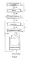
- Such monitor device 51 generally comprises a display device 52, a brightness control device 53 and a lighting device 4 as shown in Fig. 4.
- the display device 52 separates and demodulates the luminance signal, the carrier chrominance signal, and the color burst-signal from an input image signal and reproduces primary color signals RGB. Further, the display device 52 separates synchronizing signals (a horizontal synchronizing signal and a vertical synchronizing signal) from the image signal and varies the brightness of each RGB pixel composing the display screen 52a in response to the respective primary color signals, while the display screen 52a is scanned in a horizontal direction and a vertical direction by the horizontal and vertical synchronizing signals in each period. Hence, a color image can be displayed on the display screen 52a.
- synchronizing signals a horizontal synchronizing signal and a vertical synchronizing signal
- the brightness control device 53 comprises a light sensor 3a, a filter 3b and a control portion 53c.
- the light sensor 3a detects the ambient light and outputs as a detecting signal S1 a DC voltage.
- the filter 3b has a comparatively large time constant to remove a noise component (a high frequency component) in the detecting signal S1 and outputs as a detecting signal S2 a voltage which corresponds to the average ambient brightness.
- the control portion 53c generates ambient light data by A/D conversion of the detecting signal S2 and produces, based on this ambient light data, a PWM (Pulse Width Modulation) signal Sc having a given frequency of 100 Hz or more as a brightness control signal by means of a program-controlled signal processor.
- the control portion 53c changes the duty ratio of the PWM signal Sc in response to the brightness of the ambient light.
- the lighting device 4 comprises an inverter 4a and a fluorescent lamp (back light) 4b.
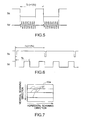
- the inverter 4a generates a driving signal Sd by intermittent oscillation of several tens of kHz, the on and off periods of the intermittent oscillation being controlled in response to the duty ratio of the PWM signal Sc, as shown in Fig. 5.
- the fluorescent lamp 4b flashes on and off since it is driven by this driving signal Sd.
- the flashing period of the fluorescent lamp 4b that is the frequency fc of the PWM signal Sc (period Tc) is equal to or larger than 100 Hz.
- flashing of the fluorescent lamp 4b (flicker) is not sensed by human eyes.
- brightness of the display screen 52a lighted up by illumination-light L from the fluorescent lamp 4b is merely recognized as average brightness corresponding to the duty ratio of the PWM signal Sc.
- the brightness of the display screen 52a in the display device 52 is increased by controlling the duty ratio of the PWM signal Sc to be relatively large.
- the images can be recognized well even in bright environment.
- the brightness on the display screen 52a in the display device 52 is decreased by controlling the duty ratio of the PWM signal Sc to be relatively small.
- the images can be recognized without dazzling.
- this conventional brightness control device 53 and the monitor device 51 include the following problems. Namely, the frequency fc of the PWM signal Sc is determined without considering the vertical synchronization frequency fv (the frequency of the vertical synchronizing signal Sv) of the image signal inputted to the display device 52.
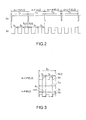
- the frequency fc of the PWM signal Sc (period Tc) is an integral multiple (2 as an example in this figure) of the frequency fv (period Tv)
- each rising edge and falling edge of the PWM signal Sc is always at the same position every vertical scanning period (every field). In this case, switching noise occurs synchronously with this rising and falling edges of the PWM signal Sc since the inverter 4a is turned on and off synchronously with it.
- the main object of the present invention is to provide a brightness control device that can substantially reduce or even avoid these lateral stripes.
- Another object of the present invention is to provide a monitor device using such brightness control device.
- the frequency of a brightness control signal is controlled to depend on the vertical synchronization frequency of the image signal to be displayed on a display device. This allows preventing the frequency of the brightness control signal to be an integer multiple of the vertical synchronization frequency of the image signal. With the frequency of the brightness control signal not being an integer multiple of the vertical synchronization frequency of the image signal the rising edges and falling edges of the brightness control signal continuously shift relative to the vertical synchronizing signal, i.e., they are at different positions each vertical scanning. Thus, switching noise of an inverter that would otherwise occur and manifest itself as lateral stripes on the screen can be avoided or sufficiently reduced.
- the structure of the monitor device 1 is described with reference to the Fig. 1.
- Structural elements same or similar to those in the monitor device 51 are denoted with the same reference numerals.
- the monitor device 1 is a multi-frequency monitor device capable of receiving image signals of either the PAL or SECAM system or the NTSC system. As shown in Fig. 1, monitor device 1 comprises a display device 2, a brightness control device 3 and the lighting device 4.
- the display device 2 consists of a liquid crystal display device, for example.
- the display device 2 reproduces primary color signals corresponding to RGB by separating and demodulating a luminance signal, a carrier chrominance signal and a color burst- signal from an input image signal.
- the display device 52 separates synchronizing signals (a horizontal synchronizing signal and a vertical synchronizing signal) from the image signal and varies the brightness of each RGB pixel composing the display screen 2a in response to the primary color signals while the display screen 2a is scanned in the horizontal direction and the vertical direction each period of each synchronizing signal. Further, the display device 2 detects the vertical synchronization frequency fv and produces corresponding frequency data Df.
- synchronizing signals a horizontal synchronizing signal and a vertical synchronizing signal
- the brightness control device 3 comprises the light sensor 3a, the filter 3b and a control portion 3c.
- the light sensor 3a detects the brightness of ambient light and outputs the detecting signal 31.
- the detecting signal S1 includes an irregular noise component (a high frequency component) corresponding to a little instant changes of ambient light which cannot be recognized by a human eye.
- the filter 3b removes this noise component from the detecting signal S1 and outputs the detecting signal S2.
- the control portion 3c comprises an analog-to-digital (A/D) converter, a CPU and an internal memory, for example.
- the A/D converter converts the detecting signal S2 into digital ambient light data representing the brightness of the ambient light.
- a CPU is operated in accordance with a program stored in an internal memory and produces the PWM signal (the brightness control signal) Sc based on the ambient light data and frequency data Df generated by the display device 2.
- the CPU produces the PWM signal Sc by utilizing a programmed timer that is operated by the clock signal used for CPU operation. Further, the CPU determines the frequency fc of the PWM signal Sc based on the frequency of the vertical synchronization frequency fv specified by the frequency data Df in accordance with expression (1) when the PWM signal Sc is generated.
- Expression (1) is stored in the internal memory beforehand. Furthermore, CPU determines the duty ratio of the PWM signal Sc based on the ambient light data.
- fc (n ⁇ 1/2) x fv
- n is a natural number, and the frequency fc of the PWM signal Sc is higher than 100 Hz according to the present embodiment. Thus, flicker can be reduced.
- the lighting device 4 comprises the inverter 4a and the fluorescent lamp 4b.
- the inverter 4a produces the driving signal Sd shown in Fig. 5 by intermittent oscillation of several tens of kHz in response to the duty ratio of the PWM signal Sc.
- the fluorescent lamp 4b is driven by the driving signal Sd and flashes on and off thereby. Hence, it generates illumination light L irradiating onto the display device 2.
- the display device 2 displays an image on the display screen 2a based on an image signal.
- the display device 2 detects the frequency (the vertical synchronization frequency) fv of the vertical synchronizing signal Sv separated from the image signal and produces corresponding frequency data Df.
- frequency data Df of the value 60 is generated since the value of vertical synchronization frequency fv of an NTSC image signal is 60 Hz.
- the period of the vertical synchronizing signal Sv is denoted Tv herein.
- the light sensor 3a detects the brightness of the ambient light and generates the detecting signal S1.
- the filter 3b removes a noise component from the detecting signal S1 and outputs the detecting signal S2.
- the control portion 3c produces ambient light data based on the detecting signal S2.
- the control portion 3c determines the frequency fc of the PWM signal Sc by inserting frequency data Df into expression (1).
- the control portion 3c determines the duty ratio of the PWM signal Sc based on the ambient light data, and the PWM signal Sc shown in Fig. 2 is produced based on the frequency fc and duty ratio as determined.
- the period of the PWM signal Sc is denoted Tc.
- the inverter 4a generates the driving signal Sd by intermittent oscillation at a frequency of several tens of kHz, the on and off periods of the intermittent oscillation being controlled in response to the duty ratio of the PWM signal Sc.
- the fluorescent lamp 4b flashes on and off, and lights up the display screen 2a with illumination light L.
- the amount of light of the illumination light L is determined by the duty ratio of the PWM signal Sc.
- the display screen 2a of a the display device 2 is lighted up with illumination light L whose brightness corresponds to that of the ambient light, i.e. is automatically controlled (dimmer control).
- frequency fc of the PWM signal Sc is always set automatically to a multiple of the vertical synchronization frequency fv of the input image signal, the multiple being a value in the middle between two successive integers.
- the PWM signal Sc becomes maximally asynchronous with respect to the vertical synchronizing signal Sv.
- the rising edges and the falling edges of the PWM signals Sc in successive fields do not coincide.
- switching noise caused by the inverter 4a switching between on and off operations of its intermittent oscillation synchronously with a rising (or falling) edge and a falling (or rising) edge of the PWM signal Sc, occurs at the same timing every vertical scanning. Therefore, with the monitor device 1, lateral stripes (dimmer control stripes) ST occurring on the display screen 2a due to switching noise, can be sufficiently reduced irrespective of the vertical synchronization frequency fv. Even if a frequency of the PWM signal Sc fluctuates to some extent, due to constants of used electronic components changing with the ambient temperature, the frequency of the PWM signal Sc can be kept asynchronous with respect to the vertical synchronizing signal Sv. Hence, lateral stripes occurring on the display screen 2a caused by switching noise can be significantly reduced.
- the frequency fc of the PWM signal Sc is determined using the plus sign (+) in expression (1).
- the minus sign (-) may be used instead as long as the resulting frequency fc of the PWM signal Sc is high enough to prevent flickering.
- the present invention can be applied to a mono-frequency monitor device, i.e., one adapted to process image signals of only one predetermined vertical synchronization frequency fv, e.g., a PAL or SECAM signal or an NTSC signal.
- a mono-frequency monitor device i.e., one adapted to process image signals of only one predetermined vertical synchronization frequency fv, e.g., a PAL or SECAM signal or an NTSC signal.
- lateral stripes can be significantly reduced as with the multi-frequency monitor device of the foregoing embodiment.
- the frequency fc of the PWM signal Sc produced by the brightness control device is preset to be (n ⁇ 1/2) times the predetermined one vertical synchronization frequency fv.
- a single expression namely expression (1), is used for determining the frequency fc of the PWM signal Sc.
- a plurality of expressions for determining the frequency fc of the PWM signal Sc may be prepared in advance, and then, one of these expressions selected depending on the vertical synchronization frequency fv of the input image signal. An example will be used to explain this in more detail.
- a multi-frequency monitor device where either signal, a PAL or SECAM image signal and an NTSC image signal, can be inputted.
- the basic configuration of this monitor device is the same as that of the monitor device 1 in the embodiment explained above and the same elements will be denoted by the same reference numbers.
- the vertical synchronization frequency fvP of a PAL image signal and that of a SECAM image signal is 50 Hz
- the vertical synchronization frequency fvN of an NTSC image signal is 60 Hz.
- the CPU of the control portion 3c selects one of these expressions (2) and (3) depending on the frequency data Df.
- the frequency fc (fcN, fcP) of the PWM signal Sc is determined by inserting the vertical synchronization frequency fv (fvN, fvP), specified by the frequency data Df, into the selected expression.
- the CPU calculates the frequency fcN of the PWM signal Sc based on the expression (2) when the frequency data Df represents a value of 60 (namely, when an NTSC image signal is inputted); and it calculates the frequency fcP of the PWM signal Sc based on the expression (3) when the frequency data Df represents a value of 50 (namely, when a PAL or SECAM image signal is inputted).
- n 1
- the frequency fcN of the PWM signal Sc becomes 270 Hz (or 330 Hz) when the frequency data Df represents a value of 60
- the frequency fcP of the PWM signal Sc becomes 275 Hz (or 325 Hz) when the frequency data Df represents a value of 50.
- the difference between the frequencies fcN and fcP can always be kept at only 5 Hz in this example. Therefore, modification of the contents of software (a program for processing) can be reduced when the frequencies fcN and fcP are to be switched.
- the CPU of the control portion 3c determines the duty ratio of the PWM signal Sc for each of the frequencies fcN and fcP based on the ambient light data.
- the duty ratio of the PWM signal Sc for the frequency fcN and that for fcP are the same when the brightness of ambient light is the same.
- the inverter's output signal is a little bit smaller at the begin of each on period due to the transient response of the inverter 4a.
- the duty ratios of the PWM signal Sc for the frequencies fcN and fcP are the same in this multi-frequency monitor device and the difference between the frequencies fcN and fcP can always be kept at only 5 Hz, the brightness difference of the display screen 2a between modes for NTSC signals and PAL (SECAM) signals can be minimized to be negligible. Hence, the quality of dimmer control of a multi-frequency monitor can be improved.
- the present invention has been described with reference to a multi-frequency monitor device displaying an image signal of either the NTSC system or the PAL (SECAM) system.
- the present invention is applicable not only to the cases where the vertical synchronization frequency fv is 50 Hz or 60 Hz, but can also be applied to multi-frequency monitor devices for displaying image signals of any other vertical synchronization frequency fv.
- a signal having a luminance signal, a carrier chrominance signal, a color burst signal and synchronizing signals integrated as an image signal is inputted.
- the present invention can also be applied to monitor devices into which an image signal is inputted, in which, for example, synchronizing signals are separated from other signals.
- an oscillator including a PLL or DDS (Direct Digital Synthesizer) for producing the PWM signal Sc may provided so that the control portion 3c can switch the oscillation frequency of such oscillator.
Abstract
Description
- The present invention relates to a brightness control device which controls brightness of a display screen in a display device by controlling the duty ratio of a brightness control signal applied to an inverter type lighting device. The invention also relates to a monitor device having such brightness control device.
- It is preferable that in a monitor device the brightness of a display screen can be controlled appropriately (dimmer control) in response to the brightness of the operating environment. This helps improving sight recognition and reducing fatigue of eyes caused by long time use. In particular, the monitor device of a car navigation system is widely used under an environment having large differences of brightness and darkness from bright daylight to night with hardly any ambient light. Therefore, brightness control of a display screen is required. It is a common technique to control the brightness in response the lamps of the automobile being turned on or off, or to control the brightness depending on the brightness of ambient light as detected through a light sensor.
-
Such monitor device 51 generally comprises adisplay device 52, abrightness control device 53 and alighting device 4 as shown in Fig. 4. - The
display device 52 separates and demodulates the luminance signal, the carrier chrominance signal, and the color burst-signal from an input image signal and reproduces primary color signals RGB. Further, thedisplay device 52 separates synchronizing signals (a horizontal synchronizing signal and a vertical synchronizing signal) from the image signal and varies the brightness of each RGB pixel composing thedisplay screen 52a in response to the respective primary color signals, while thedisplay screen 52a is scanned in a horizontal direction and a vertical direction by the horizontal and vertical synchronizing signals in each period. Hence, a color image can be displayed on thedisplay screen 52a. - The
brightness control device 53 comprises alight sensor 3a, afilter 3b and acontrol portion 53c. Thelight sensor 3a detects the ambient light and outputs as a detecting signal S1 a DC voltage. Thefilter 3b has a comparatively large time constant to remove a noise component (a high frequency component) in the detecting signal S1 and outputs as a detecting signal S2 a voltage which corresponds to the average ambient brightness. Thecontrol portion 53c generates ambient light data by A/D conversion of the detecting signal S2 and produces, based on this ambient light data, a PWM (Pulse Width Modulation) signal Sc having a given frequency of 100 Hz or more as a brightness control signal by means of a program-controlled signal processor. Thecontrol portion 53c changes the duty ratio of the PWM signal Sc in response to the brightness of the ambient light. - The
lighting device 4 comprises aninverter 4a and a fluorescent lamp (back light) 4b. Theinverter 4a generates a driving signal Sd by intermittent oscillation of several tens of kHz, the on and off periods of the intermittent oscillation being controlled in response to the duty ratio of the PWM signal Sc, as shown in Fig. 5. Thefluorescent lamp 4b flashes on and off since it is driven by this driving signal Sd. The flashing period of thefluorescent lamp 4b, that is the frequency fc of the PWM signal Sc (period Tc) is equal to or larger than 100 Hz. Hence, flashing of thefluorescent lamp 4b (flicker) is not sensed by human eyes. Thus, brightness of thedisplay screen 52a lighted up by illumination-light L from thefluorescent lamp 4b is merely recognized as average brightness corresponding to the duty ratio of the PWM signal Sc. - Therefore, in this
monitor device 51, during daylight time when the ambient light is bright, the brightness of thedisplay screen 52a in thedisplay device 52 is increased by controlling the duty ratio of the PWM signal Sc to be relatively large. As a result of the increased brightness of images displayed on thedisplay screen 52a, the images can be recognized well even in bright environment. On the other hand, during the time from the evening to the night when the ambient light becomes darker, the brightness on thedisplay screen 52a in thedisplay device 52 is decreased by controlling the duty ratio of the PWM signal Sc to be relatively small. As a result of the decreased brightness of the images displayed on thedisplay screen 52a, the images can be recognized without dazzling. - However, this conventional
brightness control device 53 and themonitor device 51 include the following problems. Namely, the frequency fc of the PWM signal Sc is determined without considering the vertical synchronization frequency fv (the frequency of the vertical synchronizing signal Sv) of the image signal inputted to thedisplay device 52. Hence, as shown in Fig. 6, when the frequency fc of the PWM signal Sc (period Tc) is an integral multiple (2 as an example in this figure) of the frequency fv (period Tv), each rising edge and falling edge of the PWM signal Sc is always at the same position every vertical scanning period (every field). In this case, switching noise occurs synchronously with this rising and falling edges of the PWM signal Sc since theinverter 4a is turned on and off synchronously with it. Hence, this switching noise always occurs every field. Therefore, as shown in Fig. 7, lateral stripes (dimmer control stripes) ST caused by such switching noise being piled up every vertical scanning period show up in a given location (fixed location) on thedisplay screen 52a. This deteriorates the display quality of themonitor device 51. This problem also occurs in a multi-frequency monitor device which is designed to display a normal image irrespective of whether, for example, an NTSC image signal (whose vertical synchronization frequency is 60 Hz) or a PAL (or SECAM ) image signal (whose vertical synchronization frequency is 50 Hz) is inputted. - In order to overcome the above-mentioned problem, the main object of the present invention is to provide a brightness control device that can substantially reduce or even avoid these lateral stripes. Another object of the present invention is to provide a monitor device using such brightness control device.
- This object is achieved by a brightness control device as claimed in
claim 1 and a monitor device as claimed inclaim 4. Preferred embodiments of the invention are subject-matter of the dependent claims. - According to the present invention, the frequency of a brightness control signal is controlled to depend on the vertical synchronization frequency of the image signal to be displayed on a display device. This allows preventing the frequency of the brightness control signal to be an integer multiple of the vertical synchronization frequency of the image signal. With the frequency of the brightness control signal not being an integer multiple of the vertical synchronization frequency of the image signal the rising edges and falling edges of the brightness control signal continuously shift relative to the vertical synchronizing signal, i.e., they are at different positions each vertical scanning. Thus, switching noise of an inverter that would otherwise occur and manifest itself as lateral stripes on the screen can be avoided or sufficiently reduced. Preferred embodiments of the present invention will be explained hereinafter with reference to the accompanying drawings, in which:
- Fig. 1 shows a block diagram of the
monitor device 1 according to one embodiment of the present invention, - Fig. 2 shows a timing chart of the vertical synchronizing signal Sv and the PWM signal Sc,
- Fig. 3 shows a timing chart illustrating the situation when the rising or falling edge of the PWM signal Sc is shifted every period of the vertical synchronizing signal Sv,
- Fig. 4 shows a block diagram of the
monitor device 51, - Fig. 5 shows a timing chart of the relationship of the PWM signal Sc with the driving signal Sd in the
monitor device 51 and themonitor device 1, - Fig. 6 shows a timing chart of the relationship of the vertical synchronizing signal Sv with the PWM signal Sc in the
monitor device 51, and - Fig. 7 shows the
display screen 52a of themonitor device 51 with dimmer control stripes. - Firstly, the structure of the
monitor device 1 is described with reference to the Fig. 1. Structural elements same or similar to those in themonitor device 51 are denoted with the same reference numerals. - The
monitor device 1 is a multi-frequency monitor device capable of receiving image signals of either the PAL or SECAM system or the NTSC system. As shown in Fig. 1,monitor device 1 comprises adisplay device 2, abrightness control device 3 and thelighting device 4. Thedisplay device 2 consists of a liquid crystal display device, for example. Thedisplay device 2 reproduces primary color signals corresponding to RGB by separating and demodulating a luminance signal, a carrier chrominance signal and a color burst- signal from an input image signal. Further, thedisplay device 52 separates synchronizing signals (a horizontal synchronizing signal and a vertical synchronizing signal) from the image signal and varies the brightness of each RGB pixel composing thedisplay screen 2a in response to the primary color signals while thedisplay screen 2a is scanned in the horizontal direction and the vertical direction each period of each synchronizing signal. Further, thedisplay device 2 detects the vertical synchronization frequency fv and produces corresponding frequency data Df. - The
brightness control device 3 comprises thelight sensor 3a, thefilter 3b and acontrol portion 3c. Thelight sensor 3a detects the brightness of ambient light and outputs the detecting signal 31. The detecting signal S1 includes an irregular noise component (a high frequency component) corresponding to a little instant changes of ambient light which cannot be recognized by a human eye. Thefilter 3b removes this noise component from the detecting signal S1 and outputs the detecting signal S2. Thecontrol portion 3c comprises an analog-to-digital (A/D) converter, a CPU and an internal memory, for example. The A/D converter converts the detecting signal S2 into digital ambient light data representing the brightness of the ambient light. A CPU is operated in accordance with a program stored in an internal memory and produces the PWM signal (the brightness control signal) Sc based on the ambient light data and frequency data Df generated by thedisplay device 2. In this embodiment, the CPU produces the PWM signal Sc by utilizing a programmed timer that is operated by the clock signal used for CPU operation. Further, the CPU determines the frequency fc of the PWM signal Sc based on the frequency of the vertical synchronization frequency fv specified by the frequency data Df in accordance with expression (1) when the PWM signal Sc is generated. Expression (1) is stored in the internal memory beforehand. Furthermore, CPU determines the duty ratio of the PWM signal Sc based on the ambient light data.
- In expression (1) n is a natural number, and the frequency fc of the PWM signal Sc is higher than 100 Hz according to the present embodiment. Thus, flicker can be reduced. An example will be explained hereinafter, in which n=2 is assumed and the alternative (n+1/2) is used in order to increase the frequency fc (rather than reducing it as would be the case with (n-1/2)).
- The
lighting device 4 comprises theinverter 4a and thefluorescent lamp 4b. Theinverter 4a produces the driving signal Sd shown in Fig. 5 by intermittent oscillation of several tens of kHz in response to the duty ratio of the PWM signal Sc. Thefluorescent lamp 4b is driven by the driving signal Sd and flashes on and off thereby. Hence, it generates illumination light L irradiating onto thedisplay device 2. - Next, the operation of the
monitor device 1 is explained using an NTSC image signal as an example. - The
display device 2 displays an image on thedisplay screen 2a based on an image signal. At the same time, thedisplay device 2 detects the frequency (the vertical synchronization frequency) fv of the vertical synchronizing signal Sv separated from the image signal and produces corresponding frequency data Df. In this case, frequency data Df of the value 60 is generated since the value of vertical synchronization frequency fv of an NTSC image signal is 60 Hz. The period of the vertical synchronizing signal Sv is denoted Tv herein. - On the other hand, the
light sensor 3a detects the brightness of the ambient light and generates the detecting signal S1. Thefilter 3b removes a noise component from the detecting signal S1 and outputs the detecting signal S2. Subsequently thecontrol portion 3c produces ambient light data based on the detecting signal S2. Furthermore, thecontrol portion 3c determines the frequency fc of the PWM signal Sc by inserting frequency data Df into expression (1). In this case, the frequency fc of the PWM signal Sc is given by the following equation since the frequency data Df represents the value 60:
- The
control portion 3c determines the duty ratio of the PWM signal Sc based on the ambient light data, and the PWM signal Sc shown in Fig. 2 is produced based on the frequency fc and duty ratio as determined. The period of the PWM signal Sc is denoted Tc. - The
inverter 4a generates the driving signal Sd by intermittent oscillation at a frequency of several tens of kHz, the on and off periods of the intermittent oscillation being controlled in response to the duty ratio of the PWM signal Sc. Driven by the driving signal Sd thefluorescent lamp 4b flashes on and off, and lights up thedisplay screen 2a with illumination light L. The amount of light of the illumination light L is determined by the duty ratio of the PWM signal Sc. As a result, thedisplay screen 2a of a thedisplay device 2 is lighted up with illumination light L whose brightness corresponds to that of the ambient light, i.e. is automatically controlled (dimmer control). - In the embodiment described so far, frequency fc of the PWM signal Sc is always set automatically to a multiple of the vertical synchronization frequency fv of the input image signal, the multiple being a value in the middle between two successive integers. As shown in Fig. 2, this results in the rising and falling edges of the PWM signal Sc being shifted by Tc/2 every vertical scanning (field). In other words, the PWM signal Sc becomes maximally asynchronous with respect to the vertical synchronizing signal Sv. As a result, as shown in Fig. 3, the rising edges and the falling edges of the PWM signals Sc in successive fields do not coincide. Hence, it can be avoided that switching noise, caused by the
inverter 4a switching between on and off operations of its intermittent oscillation synchronously with a rising (or falling) edge and a falling (or rising) edge of the PWM signal Sc, occurs at the same timing every vertical scanning. Therefore, with themonitor device 1, lateral stripes (dimmer control stripes) ST occurring on thedisplay screen 2a due to switching noise, can be sufficiently reduced irrespective of the vertical synchronization frequency fv. Even if a frequency of the PWM signal Sc fluctuates to some extent, due to constants of used electronic components changing with the ambient temperature, the frequency of the PWM signal Sc can be kept asynchronous with respect to the vertical synchronizing signal Sv. Hence, lateral stripes occurring on thedisplay screen 2a caused by switching noise can be significantly reduced. - The present invention is not limited to the above-mentioned embodiment. For instance, in the above example, the frequency fc of the PWM signal Sc is determined using the plus sign (+) in expression (1). The minus sign (-) may be used instead as long as the resulting frequency fc of the PWM signal Sc is high enough to prevent flickering.
- Furthermore, the present invention can be applied to a mono-frequency monitor device, i.e., one adapted to process image signals of only one predetermined vertical synchronization frequency fv, e.g., a PAL or SECAM signal or an NTSC signal. In this case lateral stripes (dimmer control stripes) can be significantly reduced as with the multi-frequency monitor device of the foregoing embodiment.
- In this case, the frequency fc of the PWM signal Sc produced by the brightness control device is preset to be (n ± 1/2) times the predetermined one vertical synchronization frequency fv.
- Further, according to the above embodiment, a single expression, namely expression (1), is used for determining the frequency fc of the PWM signal Sc. Instead, a plurality of expressions for determining the frequency fc of the PWM signal Sc may be prepared in advance, and then, one of these expressions selected depending on the vertical synchronization frequency fv of the input image signal. An example will be used to explain this in more detail.
- Assume a multi-frequency monitor device where either signal, a PAL or SECAM image signal and an NTSC image signal, can be inputted. The basic configuration of this monitor device is the same as that of the
monitor device 1 in the embodiment explained above and the same elements will be denoted by the same reference numbers. The vertical synchronization frequency fvP of a PAL image signal and that of a SECAM image signal is 50 Hz, whereas the vertical synchronization frequency fvN of an NTSC image signal is 60 Hz. For these cases the following expressions are stored beforehand in the internal memory of thecontrol portion 3c, where n is a natural number:

- In this multi-frequency monitor device, the CPU of the
control portion 3c selects one of these expressions (2) and (3) depending on the frequency data Df. The frequency fc (fcN, fcP) of the PWM signal Sc is determined by inserting the vertical synchronization frequency fv (fvN, fvP), specified by the frequency data Df, into the selected expression. More specifically, the CPU calculates the frequency fcN of the PWM signal Sc based on the expression (2) when the frequency data Df represents a value of 60 (namely, when an NTSC image signal is inputted); and it calculates the frequency fcP of the PWM signal Sc based on the expression (3) when the frequency data Df represents a value of 50 (namely, when a PAL or SECAM image signal is inputted). According to this, in case of n =1, the frequency fcN of the PWM signal Sc becomes 270 Hz (or 330 Hz) when the frequency data Df represents a value of 60, and the frequency fcP of the PWM signal Sc becomes 275 Hz (or 325 Hz) when the frequency data Df represents a value of 50. Thus, the difference between the frequencies fcN and fcP can always be kept at only 5 Hz in this example. Therefore, modification of the contents of software (a program for processing) can be reduced when the frequencies fcN and fcP are to be switched. - Further, the CPU of the
control portion 3c determines the duty ratio of the PWM signal Sc for each of the frequencies fcN and fcP based on the ambient light data. Thus, the duty ratio of the PWM signal Sc for the frequency fcN and that for fcP are the same when the brightness of ambient light is the same. As shown in Fig. 5, when on/off operation of theinverter 4a is controlled with the PWM signal Sc, the inverter's output signal is a little bit smaller at the begin of each on period due to the transient response of theinverter 4a. Because the duty ratios of the PWM signal Sc for the frequencies fcN and fcP are the same in this multi-frequency monitor device and the difference between the frequencies fcN and fcP can always be kept at only 5 Hz, the brightness difference of thedisplay screen 2a between modes for NTSC signals and PAL (SECAM) signals can be minimized to be negligible. Hence, the quality of dimmer control of a multi-frequency monitor can be improved. - So far the present invention has been described with reference to a multi-frequency monitor device displaying an image signal of either the NTSC system or the PAL (SECAM) system. However, the present invention is applicable not only to the cases where the vertical synchronization frequency fv is 50 Hz or 60 Hz, but can also be applied to multi-frequency monitor devices for displaying image signals of any other vertical synchronization frequency fv.
- Furthermore, described so far was the case that a signal having a luminance signal, a carrier chrominance signal, a color burst signal and synchronizing signals integrated as an image signal, is inputted. However, the present invention can also be applied to monitor devices into which an image signal is inputted, in which, for example, synchronizing signals are separated from other signals. Furthermore, an oscillator including a PLL or DDS (Direct Digital Synthesizer) for producing the PWM signal Sc may provided so that the
control portion 3c can switch the oscillation frequency of such oscillator.
Claims (4)
- A brightness control device for controlling the brightness of a display screen (2a) in a display device (2), to which an input image signal is applied, by controlling the duty ratio of a brightness control signal applied to an inverter type lighting device (4), wherein the frequency of the brightness control signal (Sc) is set to be a non-integer multiple of the vertical synchronization frequency of the input image signal.
- The device according to claim 1, wherein the frequency of the brightness control signal (Sc) is set to (n+1/2) times the vertical synchronization frequency, n being a natural number.
- The device according to claim 1, whereinthe frequency of the brightness control signal (Sc) is set to (6n±1/2) times the vertical synchronization frequency, when the input image signal is one of the PAL or the SECAM system, andthe frequency of the brightness control signal (Sc) is set to (5n±1/2) times the vertical synchronization frequency, when the input image signal is one of the NTSC system.
- A monitor device, comprising;the display device (2) which is capable of displaying image signals of different vertical synchronization frequencies,the inverter type lighting device (4) for lighting up the display screen (2a) of the display device (2),and the brightness control device (3) according to any one of claim 1 to 3 for controlling the brightness of the display screen (2a) by controlling the duty ratio of the brightness control signal (Sc) applied to the lighting device (4).
Applications Claiming Priority (2)
| Application Number | Priority Date | Filing Date | Title |
|---|---|---|---|
| JP2002059581A JP3610958B2 (en) | 2002-03-05 | 2002-03-05 | Luminance control device and monitor device |
| JP2002059581 | 2002-03-05 |
Publications (2)
| Publication Number | Publication Date |
|---|---|
| EP1343135A2 true EP1343135A2 (en) | 2003-09-10 |
| EP1343135A3 EP1343135A3 (en) | 2005-02-16 |
Family
ID=27751123
Family Applications (1)
| Application Number | Title | Priority Date | Filing Date |
|---|---|---|---|
| EP03004510A Withdrawn EP1343135A3 (en) | 2002-03-05 | 2003-02-28 | Brightness control device and display device with duty ratio control of a lighting device |
Country Status (3)
| Country | Link |
|---|---|
| US (1) | US20040008176A1 (en) |
| EP (1) | EP1343135A3 (en) |
| JP (1) | JP3610958B2 (en) |
Cited By (2)
| Publication number | Priority date | Publication date | Assignee | Title |
|---|---|---|---|---|
| EP1665220A1 (en) * | 2003-09-15 | 2006-06-07 | Intel Corporation | Automatic image luminance control with backlight adjustment |
| EP1678552A1 (en) * | 2003-10-28 | 2006-07-12 | Samsung Electronics Co., Ltd. | Display and control method thereof |
Families Citing this family (35)
| Publication number | Priority date | Publication date | Assignee | Title |
|---|---|---|---|---|
| US7292221B2 (en) * | 2003-03-20 | 2007-11-06 | Lg Electronics Inc. | Apparatus and method for controlling inverter pulse width modulation frequency in LCD in portable computer |
| KR100673689B1 (en) * | 2003-03-20 | 2007-01-23 | 엘지전자 주식회사 | Apparatus and method for controling invertor pulse width modulation frequency in portable computer |
| KR100943715B1 (en) * | 2003-04-21 | 2010-02-23 | 삼성전자주식회사 | Power Supply, Liquid Crystal Display Device And Driving Method For The Same |
| KR20050032319A (en) * | 2003-10-01 | 2005-04-07 | 삼성에스디아이 주식회사 | Field emission display and deriving method thereof |
| KR100927608B1 (en) * | 2003-10-09 | 2009-11-23 | 삼성에스디아이 주식회사 | A luminance control method and apparatus in an image display apparatus |
| KR100985858B1 (en) | 2004-04-27 | 2010-10-08 | 삼성전자주식회사 | Liquid crystal display apparatus |
| JP2005316298A (en) * | 2004-04-30 | 2005-11-10 | Nec Lcd Technologies Ltd | Liquid crystal display device, light source driving circuit used for the liquid crystal display device, and light source driving method |
| JP2006119206A (en) * | 2004-10-19 | 2006-05-11 | Toshiba Matsushita Display Technology Co Ltd | Liquid crystal display |
| US7538755B2 (en) * | 2004-11-02 | 2009-05-26 | Avago Technologies Ecbu Ip (Singapore) Pte. Ltd. | System, method and apparatus using addressable light sensors |
| US20080198117A1 (en) * | 2005-03-11 | 2008-08-21 | Takeshi Kumakura | Display Device, Liquid Crystal Monitor, Liquid Crystal Television Receiver, and Display Method |
| JPWO2006095743A1 (en) * | 2005-03-11 | 2008-08-14 | シャープ株式会社 | Display device, liquid crystal monitor, liquid crystal television receiver and display method |
| US7327097B2 (en) * | 2005-03-21 | 2008-02-05 | Hannstar Display Corporation | Light module with control of luminance and method for managing the luminance |
| TWI260567B (en) * | 2005-06-13 | 2006-08-21 | Commence Technic Co Ltd | Direct transmission method and interface of low-voltage differential signal |
| TWI326067B (en) * | 2005-06-29 | 2010-06-11 | Mstar Semiconductor Inc | Flat display device, controller, and method for displaying images |
| JP5023709B2 (en) * | 2006-04-03 | 2012-09-12 | 株式会社デンソー | Communication system and communication apparatus |
| JP4979996B2 (en) * | 2006-06-27 | 2012-07-18 | 株式会社ダイヘン | Amplifier having discharge determination function |
| KR101255509B1 (en) * | 2006-06-30 | 2013-04-16 | 엘지디스플레이 주식회사 | Method and apparatus of driving lamp |
| KR101254735B1 (en) | 2006-09-12 | 2013-04-16 | 삼성디스플레이 주식회사 | Brightness adjusting device and liquid crystal display |
| KR100826013B1 (en) | 2006-09-27 | 2008-04-28 | 엘지전자 주식회사 | Method and apparatus for improving video quality of display device |
| JP4740888B2 (en) * | 2007-03-05 | 2011-08-03 | シャープ株式会社 | Liquid crystal display |
| WO2008123865A1 (en) * | 2007-04-05 | 2008-10-16 | Catholic Healthcare West | Method of detecting and controlling perceptual flicker |
| WO2008126904A1 (en) * | 2007-04-11 | 2008-10-23 | Taiyo Yuden Co., Ltd. | Video display device |
| JP2010141370A (en) * | 2007-04-11 | 2010-06-24 | Taiyo Yuden Co Ltd | Video display device, method thereof, signal processing circuit built in the video display device, and liquid crystal backlight driving device |
| WO2008129922A1 (en) * | 2007-04-18 | 2008-10-30 | Sharp Kabushiki Kaisha | Liquid crystal display device |
| WO2009001409A1 (en) * | 2007-06-27 | 2008-12-31 | Tamura Corporation | Controller and control method of driving frequency of light emitting substance |
| US20100277409A1 (en) * | 2008-01-22 | 2010-11-04 | Kouji Yamamoto | Terminal, method for controlling display device thereof, and recording medium where program for controlling display is recorded |
| JP2010008582A (en) * | 2008-06-25 | 2010-01-14 | Mitsubishi Electric Corp | Display |
| JP5058924B2 (en) * | 2008-09-12 | 2012-10-24 | シャープ株式会社 | Backlight unit, liquid crystal display device, and inverter dimming frequency control method |
| WO2011001726A1 (en) * | 2009-07-03 | 2011-01-06 | シャープ株式会社 | Liquid crystal display device and light source control method |
| BR112012000096A2 (en) * | 2009-07-03 | 2019-09-24 | Sharp Kk | Liquid crystal display device and light source control method. |
| TWI441142B (en) * | 2012-06-26 | 2014-06-11 | Amtran Technology Co Ltd | Liquid crystal display device capable of reducing ghost images and related method thereof |
| KR20140144539A (en) * | 2013-06-11 | 2014-12-19 | 삼성전자주식회사 | A display device and driving method of thereof |
| CN106303278B (en) * | 2016-08-29 | 2019-02-05 | Oppo广东移动通信有限公司 | Adjust the method, apparatus and photographic device of preposition photographic device user interface |
| CN110910820A (en) * | 2019-12-20 | 2020-03-24 | 京东方科技集团股份有限公司 | Display driving method and device and display system |
| CN117452699B (en) * | 2023-12-20 | 2024-03-12 | 深圳市宏瑞创展科技有限公司 | Liquid crystal display driving system and method capable of intelligently adjusting parameters |
Citations (7)
| Publication number | Priority date | Publication date | Assignee | Title |
|---|---|---|---|---|
| JPS61285429A (en) * | 1985-06-13 | 1986-12-16 | Nec Corp | Liquid crystal flat panel display |
| US5406305A (en) * | 1993-01-19 | 1995-04-11 | Matsushita Electric Industrial Co., Ltd. | Display device |
| JPH09120051A (en) * | 1995-10-25 | 1997-05-06 | Alpine Electron Inc | Light control device |
| US5844540A (en) * | 1994-05-31 | 1998-12-01 | Sharp Kabushiki Kaisha | Liquid crystal display with back-light control function |
| US5990858A (en) * | 1996-09-04 | 1999-11-23 | Bloomberg L.P. | Flat panel display terminal for receiving multi-frequency and multi-protocol video signals |
| JPH11327454A (en) * | 1998-05-15 | 1999-11-26 | Alpine Electronics Inc | Control method for luminance of lamp for backlight |
| JP2000195695A (en) * | 1998-12-28 | 2000-07-14 | Sony Corp | Back light driving method, back light driving circuit and electronic apparatus |
Family Cites Families (1)
| Publication number | Priority date | Publication date | Assignee | Title |
|---|---|---|---|---|
| JP2000241796A (en) * | 1998-12-24 | 2000-09-08 | Sharp Corp | Liquid crystal display device and electronic equipment outputting control signal of liquid crystal display device |
-
2002
- 2002-03-05 JP JP2002059581A patent/JP3610958B2/en not_active Expired - Fee Related
-
2003
- 2003-02-28 EP EP03004510A patent/EP1343135A3/en not_active Withdrawn
- 2003-03-04 US US10/379,242 patent/US20040008176A1/en not_active Abandoned
Patent Citations (7)
| Publication number | Priority date | Publication date | Assignee | Title |
|---|---|---|---|---|
| JPS61285429A (en) * | 1985-06-13 | 1986-12-16 | Nec Corp | Liquid crystal flat panel display |
| US5406305A (en) * | 1993-01-19 | 1995-04-11 | Matsushita Electric Industrial Co., Ltd. | Display device |
| US5844540A (en) * | 1994-05-31 | 1998-12-01 | Sharp Kabushiki Kaisha | Liquid crystal display with back-light control function |
| JPH09120051A (en) * | 1995-10-25 | 1997-05-06 | Alpine Electron Inc | Light control device |
| US5990858A (en) * | 1996-09-04 | 1999-11-23 | Bloomberg L.P. | Flat panel display terminal for receiving multi-frequency and multi-protocol video signals |
| JPH11327454A (en) * | 1998-05-15 | 1999-11-26 | Alpine Electronics Inc | Control method for luminance of lamp for backlight |
| JP2000195695A (en) * | 1998-12-28 | 2000-07-14 | Sony Corp | Back light driving method, back light driving circuit and electronic apparatus |
Non-Patent Citations (4)
| Title |
|---|
| PATENT ABSTRACTS OF JAPAN vol. 011, no. 151 (P-576), 16 May 1987 (1987-05-16) & JP 61 285429 A (NEC CORP), 16 December 1986 (1986-12-16) * |
| PATENT ABSTRACTS OF JAPAN vol. 1997, no. 09, 30 September 1997 (1997-09-30) -& JP 09 120051 A (ALPINE ELECTRON INC), 6 May 1997 (1997-05-06) * |
| PATENT ABSTRACTS OF JAPAN vol. 2000, no. 02, 29 February 2000 (2000-02-29) -& JP 11 327454 A (ALPINE ELECTRONICS INC), 26 November 1999 (1999-11-26) * |
| PATENT ABSTRACTS OF JAPAN vol. 2000, no. 10, 17 November 2000 (2000-11-17) & JP 2000 195695 A (SONY CORP), 14 July 2000 (2000-07-14) -& US 6 466 196 B1 (HASHIMOTO KAZUO ET AL) 15 October 2002 (2002-10-15) * |
Cited By (3)
| Publication number | Priority date | Publication date | Assignee | Title |
|---|---|---|---|---|
| EP1665220A1 (en) * | 2003-09-15 | 2006-06-07 | Intel Corporation | Automatic image luminance control with backlight adjustment |
| EP1678552A1 (en) * | 2003-10-28 | 2006-07-12 | Samsung Electronics Co., Ltd. | Display and control method thereof |
| EP1678552A4 (en) * | 2003-10-28 | 2008-10-15 | Samsung Electronics Co Ltd | Display and control method thereof |
Also Published As
| Publication number | Publication date |
|---|---|
| US20040008176A1 (en) | 2004-01-15 |
| EP1343135A3 (en) | 2005-02-16 |
| JP3610958B2 (en) | 2005-01-19 |
| JP2003255913A (en) | 2003-09-10 |
Similar Documents
| Publication | Publication Date | Title |
|---|---|---|
| EP1343135A2 (en) | Brightness control device and display device with duty ratio control of a lighting device | |
| KR0166145B1 (en) | Liquid crystal display device with back light control function | |
| EP1376528B1 (en) | Image display and displaying method | |
| US6429839B1 (en) | Liquid crystal display apparatus and electronic device for providing control signal to liquid crystal display apparatus | |
| US8547321B2 (en) | LED backlight driver synchronization and power reduction | |
| CN108269548A (en) | Display device and method for controlling backlight thereof | |
| US20080074381A1 (en) | Liquid Crystal Display and Its Light Source Driving Method | |
| JP2004177547A (en) | Method for controlling back light for liquid crystal display and its controller | |
| US20090015179A1 (en) | Backlight control device and display apparatus | |
| US20080094344A1 (en) | Display Device and Method, Recording Medium, and Program | |
| EP2337011A1 (en) | Lamp on/off operation control method, clock generation method, clock generation circuit, light source control circuit, and display device | |
| JP3968587B2 (en) | Liquid crystal television, backlight control device, and backlight control method | |
| JP2009134237A (en) | Display device | |
| US20060170645A1 (en) | Active matrix display with a scanning backlight | |
| WO2009125600A1 (en) | Liquid crystal image display unit | |
| JP2008116554A (en) | Backlight control device and video display device equipped with the backlight control device | |
| US8212765B2 (en) | Pulse width modulated dimming of multiple lamp LCD backlight using distributed microcontrollers | |
| US20090243506A1 (en) | Method and device for driving a lamp | |
| JP2000322029A (en) | Liquid crystal display device | |
| JP3968588B2 (en) | Liquid crystal television, liquid crystal display device and liquid crystal display method | |
| JP2008065228A (en) | Light emitting device and liquid crystal display device | |
| CN110992902B (en) | Display system and backlight control method thereof | |
| JP2000111873A (en) | Liquid crystal display device | |
| JP3716100B2 (en) | Liquid crystal display device | |
| EP1826745A1 (en) | Liquid crystal display device and controlling method thereof |
Legal Events
| Date | Code | Title | Description |
|---|---|---|---|
| PUAI | Public reference made under article 153(3) epc to a published international application that has entered the european phase |
Free format text: ORIGINAL CODE: 0009012 |
|
| AK | Designated contracting states |
Kind code of ref document: A2 Designated state(s): AT BE BG CH CY CZ DE DK EE ES FI FR GB GR HU IE IT LI LU MC NL PT SE SI SK TR |
|
| AX | Request for extension of the european patent |
Extension state: AL LT LV MK RO |
|
| PUAL | Search report despatched |
Free format text: ORIGINAL CODE: 0009013 |
|
| AK | Designated contracting states |
Kind code of ref document: A3 Designated state(s): AT BE BG CH CY CZ DE DK EE ES FI FR GB GR HU IE IT LI LU MC NL PT SE SI SK TR |
|
| AX | Request for extension of the european patent |
Extension state: AL LT LV MK RO |
|
| AKX | Designation fees paid | ||
| REG | Reference to a national code |
Ref country code: DE Ref legal event code: 8566 |
|
| STAA | Information on the status of an ep patent application or granted ep patent |
Free format text: STATUS: THE APPLICATION IS DEEMED TO BE WITHDRAWN |
|
| 18D | Application deemed to be withdrawn |
Effective date: 20050817 |