EP1343231A2 - A group III nitride compound semiconductor laser - Google Patents
A group III nitride compound semiconductor laser Download PDFInfo
- Publication number
- EP1343231A2 EP1343231A2 EP03005054A EP03005054A EP1343231A2 EP 1343231 A2 EP1343231 A2 EP 1343231A2 EP 03005054 A EP03005054 A EP 03005054A EP 03005054 A EP03005054 A EP 03005054A EP 1343231 A2 EP1343231 A2 EP 1343231A2
- Authority
- EP
- European Patent Office
- Prior art keywords
- layer
- semiconductor laser
- group iii
- iii nitride
- nitride compound
- Prior art date
- Legal status (The legal status is an assumption and is not a legal conclusion. Google has not performed a legal analysis and makes no representation as to the accuracy of the status listed.)
- Withdrawn
Links
Images

Classifications
-
- H—ELECTRICITY
- H01—ELECTRIC ELEMENTS
- H01S—DEVICES USING THE PROCESS OF LIGHT AMPLIFICATION BY STIMULATED EMISSION OF RADIATION [LASER] TO AMPLIFY OR GENERATE LIGHT; DEVICES USING STIMULATED EMISSION OF ELECTROMAGNETIC RADIATION IN WAVE RANGES OTHER THAN OPTICAL
- H01S5/00—Semiconductor lasers
- H01S5/30—Structure or shape of the active region; Materials used for the active region
- H01S5/34—Structure or shape of the active region; Materials used for the active region comprising quantum well or superlattice structures, e.g. single quantum well [SQW] lasers, multiple quantum well [MQW] lasers or graded index separate confinement heterostructure [GRINSCH] lasers
- H01S5/343—Structure or shape of the active region; Materials used for the active region comprising quantum well or superlattice structures, e.g. single quantum well [SQW] lasers, multiple quantum well [MQW] lasers or graded index separate confinement heterostructure [GRINSCH] lasers in AIIIBV compounds, e.g. AlGaAs-laser, InP-based laser
- H01S5/34333—Structure or shape of the active region; Materials used for the active region comprising quantum well or superlattice structures, e.g. single quantum well [SQW] lasers, multiple quantum well [MQW] lasers or graded index separate confinement heterostructure [GRINSCH] lasers in AIIIBV compounds, e.g. AlGaAs-laser, InP-based laser with a well layer based on Ga(In)N or Ga(In)P, e.g. blue laser
-
- B—PERFORMING OPERATIONS; TRANSPORTING
- B82—NANOTECHNOLOGY
- B82Y—SPECIFIC USES OR APPLICATIONS OF NANOSTRUCTURES; MEASUREMENT OR ANALYSIS OF NANOSTRUCTURES; MANUFACTURE OR TREATMENT OF NANOSTRUCTURES
- B82Y20/00—Nanooptics, e.g. quantum optics or photonic crystals
-
- H—ELECTRICITY
- H01—ELECTRIC ELEMENTS
- H01S—DEVICES USING THE PROCESS OF LIGHT AMPLIFICATION BY STIMULATED EMISSION OF RADIATION [LASER] TO AMPLIFY OR GENERATE LIGHT; DEVICES USING STIMULATED EMISSION OF ELECTROMAGNETIC RADIATION IN WAVE RANGES OTHER THAN OPTICAL
- H01S2301/00—Functional characteristics
- H01S2301/18—Semiconductor lasers with special structural design for influencing the near- or far-field
-
- H—ELECTRICITY
- H01—ELECTRIC ELEMENTS
- H01S—DEVICES USING THE PROCESS OF LIGHT AMPLIFICATION BY STIMULATED EMISSION OF RADIATION [LASER] TO AMPLIFY OR GENERATE LIGHT; DEVICES USING STIMULATED EMISSION OF ELECTROMAGNETIC RADIATION IN WAVE RANGES OTHER THAN OPTICAL
- H01S5/00—Semiconductor lasers
- H01S5/20—Structure or shape of the semiconductor body to guide the optical wave ; Confining structures perpendicular to the optical axis, e.g. index or gain guiding, stripe geometry, broad area lasers, gain tailoring, transverse or lateral reflectors, special cladding structures, MQW barrier reflection layers
- H01S5/2004—Confining in the direction perpendicular to the layer structure
-
- H—ELECTRICITY
- H01—ELECTRIC ELEMENTS
- H01S—DEVICES USING THE PROCESS OF LIGHT AMPLIFICATION BY STIMULATED EMISSION OF RADIATION [LASER] TO AMPLIFY OR GENERATE LIGHT; DEVICES USING STIMULATED EMISSION OF ELECTROMAGNETIC RADIATION IN WAVE RANGES OTHER THAN OPTICAL
- H01S5/00—Semiconductor lasers
- H01S5/20—Structure or shape of the semiconductor body to guide the optical wave ; Confining structures perpendicular to the optical axis, e.g. index or gain guiding, stripe geometry, broad area lasers, gain tailoring, transverse or lateral reflectors, special cladding structures, MQW barrier reflection layers
- H01S5/2054—Methods of obtaining the confinement
- H01S5/2081—Methods of obtaining the confinement using special etching techniques
- H01S5/209—Methods of obtaining the confinement using special etching techniques special etch stop layers
-
- H—ELECTRICITY
- H01—ELECTRIC ELEMENTS
- H01S—DEVICES USING THE PROCESS OF LIGHT AMPLIFICATION BY STIMULATED EMISSION OF RADIATION [LASER] TO AMPLIFY OR GENERATE LIGHT; DEVICES USING STIMULATED EMISSION OF ELECTROMAGNETIC RADIATION IN WAVE RANGES OTHER THAN OPTICAL
- H01S5/00—Semiconductor lasers
- H01S5/20—Structure or shape of the semiconductor body to guide the optical wave ; Confining structures perpendicular to the optical axis, e.g. index or gain guiding, stripe geometry, broad area lasers, gain tailoring, transverse or lateral reflectors, special cladding structures, MQW barrier reflection layers
- H01S5/22—Structure or shape of the semiconductor body to guide the optical wave ; Confining structures perpendicular to the optical axis, e.g. index or gain guiding, stripe geometry, broad area lasers, gain tailoring, transverse or lateral reflectors, special cladding structures, MQW barrier reflection layers having a ridge or stripe structure
Landscapes
- Physics & Mathematics (AREA)
- Optics & Photonics (AREA)
- Engineering & Computer Science (AREA)
- Nanotechnology (AREA)
- Chemical & Material Sciences (AREA)
- Condensed Matter Physics & Semiconductors (AREA)
- General Physics & Mathematics (AREA)
- Electromagnetism (AREA)
- Biophysics (AREA)
- Crystallography & Structural Chemistry (AREA)
- Life Sciences & Earth Sciences (AREA)
- Semiconductor Lasers (AREA)
- Led Devices (AREA)
Abstract
Description
- This is a patent application based on Japanese patent applications No. 2002-063811 and No. 2003-040462, which were filed on March 8, 2002 and February 19, 2003, respectively, and which are incorporated herein by reference.
- The present invention relates to a group III nitride compound semiconductor laser. Especially, the present invention relates to a group III nitride compound semiconductor laser having a ridge type of a resonator.
- A semiconductor laser which has a cladding layer and an active layer and so on made of a group III nitride compound semiconductor (AlxGayIn1-x-yN, 0≦x≦1, 0≦y≦1 and 0≦ x+y≦1) has been known. The conventional semiconductor laser is a semiconductor diode having multi-layer structure with multiple group III nitride compound semiconductor layers, which are formed on a sapphire substrate in sequence. A conventional example of the semiconductor diode, disclosed by the same applicant in Japanese Patent Laid-open No. 2000-261105, is shown in FIG. 3.
- A
semiconductor laser 900 shown in FIG. 3 has the following eight layers formed on asapphire substrate 91 in sequence: abuffer layer 92; an n-layer 93; an n-cladding layer 94; an n-guide layer 95; anactive layer 96 made of multiple quantum well (MQW) layer; a p-guide layer 97; a p-cladding layer 98; and a p-contact layer 99. As shown in FIG. 3, a cavity or a resonator part (a ridged resonator cavity of part) A is formed by using, e.g., photoresist and etching, and apositive electrode 901 and anegative electrode 902 are formed on the upper surface of the p-contact layer 99 and the etched surface of the n-layer 93, respectively. - The
active layer 96, comprising a multiple quantum well (MQW) layer, is a semiconductor layer which functions as a main layer to oscillate laser. Each carriers (holes and electrons) injected from thepositive electrode 901 and thenegative electrode 902 combine in theactive layer 96, that causes laser oscillation. The n-guide layer 95 and the p-guide layer 97 function to confine carriers into theactive layer 96. Also, the n-claddinglayer 94 and the p-cladding layer 98 function to confine laser light. And the n-layer 93 and the p-contact layer 99 are semiconductor layers which are formed in order that carriers can be injected smoothly from thenegative electrode 902 and thepositive electrode 901 to the layers existing between the n-cladding layer 94 and the p-cladding layer 98, respectively. - In order that the semiconductor laser made of group III nitride compound semiconductor can oscillate laser efficiently, the cross-section of electric current path of the semiconductor laser is, for example, narrowed by decreasing the contact area of electrodes, or by decreasing the width w of the
positive electrode 901. In addition, the above-mentioned Japanese Patent Laid-open No. 2000-261105 suggests forming a deep ridged hole injection part B. That is, a boundary between a ridged cavity part A and the ridged hole injection part B is regarded as a boundary between the p-guide layer 97 and the p-cladding layer 98. - When forming the ridged hole injection part B, however, it is not easy for all the semiconductor lasers formed on a wafer that a boundary between the ridged resonator part A and the ridged hole injection part B functions as a boundary between the p-guide layer 97 and the p-cladding layer 98. The reason is that each one of group III nitride compound semiconductor layers formed on one wafer has different thickness according to the portion on which the layer is formed. So, as discloses in the above-mentioned official gazette, the applicant of the present invention suggests completely etching the p-cladding layer 98 even if a portion of the p-guide layer 97 is etched.
- The thickness of the p-guide layer 97, however, is extremely thin, e.g., about 100 nm. So when 200 nm in thickness of p-
contact layer 99 and approximately 500 nm in thickness of p-cladding layer 98 are completely etched, the p-guide layer 97 may be damaged considerably, which may deteriorate its device characteristic as a semiconductor laser. - An object of the present invention is to form a ridged carrier injection part in a ridge type of a group III nitride compound semiconductor laser, especially in a process of manufacturing the ridge type of a group III nitride compound semiconductor laser, so as to obtain a structure which hardly damages a guide layer. Another object of the present invention is that the cross sectional shape of oscillated laser beam becomes closer to a perfect circle by forming a part of cladding layer in the ridged cavity part and controlling its thickness becomes easy.
- To achieve the above object, a first aspect of the present invention is to obtain a group III nitride compound semiconductor laser comprising a laser cavity and multiple layers which are made of group III nitride compound semiconductors and formed on a substrate. The group III nitride compound semiconductor laser comprises: a first layer, which functions as a guide layer and actually confines carriers to an active layer which functions as a main layer oscillating laser; a second layer having smaller refractive index compared with the first layer, which is formed above or on the first layer and mainly confines light to the active layer and the first layer; and a third layer which is formed between the first layer and the second layer or formed into the second layer and has larger composition of aluminum (Al) in group III elements compared with the second layer. Here forming the third layer into the second layer represents that the second layer comprises two layers and that the third layer is formed between the upper second layer and the lower second layer. Composition of the upper second layer and the lower second layer may be equivalent or not equivalent. In order that the third layer comes in the scope of the present invention, aluminum (Al) composition of the third layer may be larger than that of at least one layer of upper and the lower second layers.
- The second aspect of the present invention is that aluminum (Al) composition of group III elements in the second layer is larger than that in the first layer.
- The third aspect of the present invention is that the second layer functions as a cladding layer.
- The fourth aspect of the present invention is to obtain a group III nitride compound semiconductor laser comprising a laser cavity. The laser cavity is formed by removing multiple layers, which are made of group III nitride compound semiconductors and formed on a substrate, except the width of the laser cavity part. A carrier injection part is formed contacting to the laser cavity part by removing at least all layers on the third layer except the area corresponding to the width of an electrode formed above the second layer.
- The fifth aspect of the present invention is that the electrode is a positive electrode.
- The sixth aspect of the present invention is that aluminum (Al) composition of the third layer is larger than that of the second layer by 10% or more. That is represented by the formula x3 ≥ x2+0.1 when x3 and x2 (0≤x3, x2≤1) are aluminum (Al) compositions of the third and the second layers in all the group III elements. The seventh aspect of the present invention is that the third layer is thinner than the first layer.
- By forming the third layer having larger aluminum (Al) composition in group III elements compared with that of the second layer between the first layer which functions as a guide layer and actually confines carriers to an active layer functioning as a main layer to oscillate laser and the second layer which mainly confine light to the active layer which functions as a main layer oscillating laser and the first layer, the third layer can protect the first layer in an etching process. That is because etching rate of a group III nitride compound semiconductor becomes smaller in proportion as the aluminum (Al) composition increases, there are some time during etching the third layer. Accordingly, in a process of forming a ridged carrier injection part, a guide layer cannot be damaged even when the production is not uniform. Or because the third layer having larger aluminum (Al) composition of group III elements compared with the second layer is formed between the upper second layer and the lower second layer, forming a part of a cladding layer in the laser cavity part enables it easier to control thickness of the cladding layer formed in the laser cavity part. As a result, the cross sectional shape of oscillated laser beam becomes closer to a perfect circle (the first to the fourth aspects). And when a layer of the positive electrode side, or the second layer, has p-type conduction, manufacturing process becomes easier (the fifth aspect).
- Because the difference between the aluminum (Al) composition ratios of the second layer and the third layer is 10% or more, etching rate of the third layer becomes smaller and the etching becomes more effective (the sixth aspect). By forming the third layer thinner than the first layer, the guide layer may not be damaged without deteriorating characteristics of a laser diode or thickness of the cladding layer formed in the laser cavity part may be controlled easily (the seventh aspect).
- Other objects, features, and characteristics of the present invention will become apparent upon consideration of the following description and the appended claims with reference to the accompanying drawings, all of which form a part of the specification, and wherein reference numerals designate corresponding parts in the various figures, wherein:
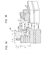
- FIG. 1A is a sectional view of a
semiconductor laser 100 in accordance with the first embodiment of the present invention; - FIG. 1B is a view showing a structure of the
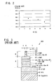
semiconductor laser 100 in accordance with the first embodiment of the present invention; - FIG. 2 is a graph showing a relation of Al composition x (0≤x≤1) in AlxGa1-xN and etching rate;
- FIG. 3 is a sectional view of a conventional semiconductor laser; and
- FIG. 4 is a view showing a structure of the
semiconductor laser 200 in accordance with the second embodiment of the present invention. - The present invention will next be described in detail with reference to embodiments, which should not be construed as limiting the invention thereto.
- FIG. 1A illustrates a sectional view of a
semiconductor laser 100. FIG. 1B illustrates a view showing a structure of thesemiconductor laser 100. - The
semiconductor laser 100 has asapphire substrate 1, and anAlN buffer layer 2 having a thickness of 50 nm is formed on thesubstrate 1. Alternatively, thebuffer layer 2 can be made of GaN, GaInN or AlGaN. On thebuffer layer 2, the following layers are formed consecutively: about 4.0µm in thickness of silicon (Si) doped gallium nitride (GaN) n-layer 3, having an electron concentration of 1 x 10¹⁸/cm-3; 500nm in thickness of Si-doped Al0.1Ga0.9N n-cladding layer 4, having an electron concentration of 1 x 10¹⁸/cm-3; 100 nm in thickness of Si-doped GaN n-guide layer 5, having an electron concentration of 1 x 10¹⁸/cm-3; and anactive layer 6 having multiple quantum well (MQW) structure in which about 35 Å in thickness of GaN barrier layer 62 and about 35 Å in thickness of Ga0.95In0.05N well layer 61 are laminated alternately. And 100 nm in thickness of magnesium (Mg) doped GaN p-guide layer 7, having a hole concentration of 5 x 10¹⁷/cm-3, 50 nm in thickness of Mg-doped Al0.25Ga0.75N p-layer 8, having a hole concentration of 5 x 10¹⁷/cm-3, 500 nm in thickness of an Mg-doped Al0.1Ga0.9N p-cladding layer 9, having a hole concentration of 5 x 10¹⁷/cm-3, and 200 nm in thickness of Mg-doped GaN p-contact layer 10, having a hole concentration of 5 x 10¹⁷/cm-3, are formed successively thereon. Alternatively, the p-contact layer 10 can be made of AlGaN or GaInN. Then 5µm in width of anelectrode 11 made of nickel (Ni) is formed on the p-contact layer 10, and anelectrode 12 made of aluminum (Al) is formed on the n-layer 3. - The ridged hole injection part B, which contacts to the ridged cavity (or resonator) part A of the
semiconductor laser 100, is formed to have a width of about 5µm, which is equal to the width w of theNi electrode 11. The ridged hole injection part B of thesemiconductor laser 100 comprises theNi electrode 11, the p-contact layer 10 and the p-cladding layer 9. And the ridged cavity part A does not comprise the p-cladding layer 9. - A method for manufacturing the
semiconductor laser 100 is explained hereinafter. Each of the layers of thesemiconductor laser 100 is formed by gaseous phase epitaxial growth, called metal organic vapor phase epitaxy (hereinafter MOVPE). The gases employed in this process were ammonia (NH3) , a carrier gas (H2 or N2), trimethyl gallium (Ga(CH3)3) (hereinafter TMG), trimethyl aluminum (Al(CH3)3) (hereinafter TMA), trimethyl indium (In(CH3)3) (hereinafter TMI), silane (SiH4), and biscyclopentadienyl magnesium (Mg(C5H5)2) (hereinafter CP2Mg). - The single
crystalline sapphire substrate 1 was placed on a susceptor in a reaction chamber for the MOVPE treatment after its main surface 'a' was cleaned by an organic washing solvent and heat treatment. Then thesapphire substrate 1 was baked for about 30 min. at 1100 °C by H2 vapor fed into the chamber at a flow rate of 2L/min. under normal pressure. - About 50 nm in thickness of
AlN buffer layer 2 was formed on the surface 'a' of thebaked sapphire substrate 1 under conditions controlled by lowering the temperature in the chamber to 400 °C, keeping the temperature constant, and concurrently supplying H2 at a flow rate of 20L/min., NH3 at 10L/min., and TMA at 18 µmol/min. for about 90 seconds. - About 4.0µm in thickness of Si-doped GaN was formed on the
buffer layer 2, as an n-layer 3 with an electron concentration of 1 x 1018cm-3, under conditions controlled by keeping the temperature of thesapphire substrate 1 at 1150°C and concurrently supplying H2 at a flow rate of 20L/min., NH3 at 10L/min., TMG at 170µmol/min., and silane (SiH4) diluted to 0.86 ppm by H2 at 2nmol/min. - About 500nm in thickness of Si-doped Al0.1Ga0.9N was formed on the n-
layer 3, as an n-cladding layer 4 with an electron concentration of 1 x 1018cm-3, under conditions controlled by keeping the temperature of thesapphire substrate 1 at 1100°C and concurrently supplying H2 at a flow rate of 20L/min., NH3 at 10L/min., TMA at 5µmol/min., TMG at 50µmol/min., and silane (SiH4) diluted to 0.86 ppm by H2 at 8nmol/min. - About 100nm in thickness of Si-doped GaN was formed on the n-cladding layer 4, as an n-
guide layer 5 with an electron concentration of 1 x 1018cm-3, under conditions controlled by keeping the temperature of thesapphire substrate 1 at 1100°C and concurrently supplying H2 at a flow rate of 20L/min., TMG at 50µmol/min., and silane (SiH4) diluted to 0.86 ppm by H2 at 8nmol/min. - About 35Å in thickness of GaN was formed on the n-
guide layer 5, as a barrier layer 62, concurrently supplying N2 or H2, NH3 and TMG. About 35Å in thickness of Ga0.95In0.05N was formed on the barrier layer 62, as awell layer 61, concurrently supplying N2 or H2, NH3, TMG and TMI.
Accordingly, four pairs of thewell layer 61 and the barrier layer 62 in total were formed, and anactive layer 6 having a multiple quantum well (MQW) structure was obtained. - About 100 nm in thickness of Mg-doped GaN was formed on the
active layer 6, as a p-guide layer 7, under conditions controlled by keeping the temperature of thesapphire substrate 1 to 1100°C, concurrently supplying N2 or H2 at a flow rate of 20L/min., NH3 at a flow rate of 10L/min., TMG at 50µmol/min., and Cp2Mg at 0.2µmol/min. - About 50nm in thickness of Mg-doped Al0.25Ga0.75N was formed on the p-
guide layer 7, as a p-layer 8, under conditions controlled by keeping the temperature of thesapphire substrate 1 to 1100°C, concurrently supplying N2 or H2 at a flow rate of 20L/min., NH3 at a flow rate of 10L/min., TMA at 15µmol/min., TMG at 50µmol/min., and Cp2Mg at 0.2µmol/min. - About 500nm in thickness of Mg-doped Al0.1Ga0.9N was formed on the p-layer 8, as a p-cladding layer 9, under conditions controlled by keeping the temperature of the
sapphire substrate 1 to 1100°C, concurrently supplying N2 or H2 at a flow rate of 20L/min., NH3 at a flow rate of 10L/min., TMA at 5µmol/min., TMG at 50µmol/min., and Cp2Mg at 0.2µmol/min. - About 200nm in thickness of Mg-doped GaN was formed on the p-cladding layer 9, as a p-
contact layer 10, under conditions controlled by keeping the temperature of thesapphire substrate 1 to 1100°C, concurrently supplying N2 or H2 at a flow rate of 20L/min., NH3 at a flow rate of 10L/min., TMG at 50µmol/min., and Cp2Mg at 0.2µmol/min. - Then, electron rays were uniformly irradiated into the three layers, or the p-
contact layer 10, the p-cladding layer 9, the p-layer 8 and the p-guide layer 7, using a reflective electron beam diffraction device. The irradiation conditions were set at 10 kV for the accelerating voltage, 1µA for the sample current, 0.2mm/s. for the speed of the beam scanning, 60µmφ for the beam aperture, and at 50µTorr vacuum. This irradiation cause to increase hole concentrations of three layers, or the p-contact layer 10, the p-cladding layer 9, the p-layer 8 and the p-guide layer 7, the respective hole concentrations are 5 x 1017cm-3, 5 x 1017cm-3 and 5 x 1017cm-3. As a result, a wafer with a multiple layer structure was obtained. - About 200nm in thickness of SiO2 layer was formed on the p-
contact layer 10 by sputtering, and a photoresist layer was laminated on the SiO2 layer. The photoresist layer of the other part except the ridged hole injection part B, or region X shown in FIG. 1A, was removed by using photolithography. And the SiO2 layer, which is not covered by the photoresist layer, was removed by using hydrofluoric acid based etching solution. - The portion of the p-
contact layer 10 and the p-cladding layer 9, which is not covered by the photoresist layer and the SiO2 layer, is dry-etched under conditions set at 0.04Torr vacuum and at 0.44W/cm2 for a high-frequency power, concurrently supplying BCl3 gas at a flow late of 10mL/min. Accordingly, the ridged hole injection part B as shown in FIG. 1B was formed. Then the SiO2 layer was removed. - In order to form an
electrode 12, region C was formed on a portion of the n-layer 3 as follows. The SiO2 layer having a thickness of 200nm was formed by carrying out sputtering, which was covered by a photoresist layer. A portion of the photoresist layer, or a portion to form region C, was removed by using photolithography. Then the SiO2 layer, which is not covered by the photoresist layer, was removed by using hydrofluoric acid based etching solution. - The p-
guide layer 7, theactive layer 6, the n-guide layer 5, the n-cladding layer 4 and a portion of the n-layer 3, which are not covered by the photoresist layer and the SiO2 layer, is dry-etched under conditions set at 0.04Torr vacuum and at 0.44W/cm2 for a high-frequency power, concurrently supplying BCl3 gas at a flow late of 10mL/min, and then dry-etched by argon (Ar) gas. Accordingly, region C shown in FIG. 1A was formed. After that the SiO2 layer was removed. - Nickel (Ni) was deposited uniformly on the
semiconductor laser 100. A photoresist layer was laminated on the Ni layer. And after removing processes using photolithography and etching, theelectrode 11 having a width of 5µm was formed on the p-contact layer 10. Aluminum (Al) was deposited on the n-layer 3, and theelectrode 12 was formed. - Accordingly, the
semiconductor laser 100 as shown in FIGS. 1A and 1B were obtained. As shown in FIG. 1A, thesemiconductor laser 100 has the ridged hole injection part B which was formed by etching all the semiconductor layers, or the p-contact layer 10 and the p-cladding layer 9, except the width of the ridged hole injection part B. Although the devices are not completely uniform, a boundary between the ridged cavity part A and the ridged hole injection part B are obtained in the p-layer 8. - For comparison, a
semiconductor laser 900 was formed as shown in FIG. 3. Thesemiconductor laser 900 is manufactured in the same process as thesemiconductor laser 100, except that thesemiconductor laser 900 does not have the p-layer 8. In one wafer of thesemiconductor laser 900 shown in FIG. 3, approximately 10% of the semiconductor laser has deteriorated device characteristic, e.g., a semiconductor laser whose guide layer 97 is largely damaged, and electric current is not adequately narrowed because etching of a cladding layer 98 is not sufficient. On the contrary, in one wafer of thesemiconductor laser 100 shown in FIG. 1, no semiconductor laser whoseguide layer 7 is largely damaged is found, and there is no problem about narrowing electric current. Thus-obtained semiconductor laser has approximately the equivalent characteristics to an acceptable product of thesemiconductor laser 900 shown in FIG. 3. - FIG. 2 illustrates a relationship between a composition ratio of aluminum and an etching rate in the experiment. As shown in FIG. 2, when a difference of composition ratio of aluminum is 10%, etching rate is different for 5%.
- FIG. 4 illustrates a sectional view of a
semiconductor laser 200 in a second embodiment of the present invention. Thesemiconductor laser 200 shown in FIG. 4 has the same structure as that of thesemiconductor laser 100 in FIG. 1 except that the following layers are laminated between the p-guide layer 7 and the p-contact layer 10 consecutively: about 20nm in thickness of magnesium (Mg) doped Al0.1Ga0.9N lower p-cladding layer 910, having a hole concentration of 5 x 10¹⁷/cm-3; about 50nm in thickness of magnesium (Mg) doped Al0.25Ga0.75N p-layer 8, having a hole concentration of 5 x 10¹⁷/cm-3; and about 420nm in thickness of magnesium (Mg) doped Al0.1Ga0.9N upper p-cladding layer 920, having a hole concentration of 5 x 10¹⁷/cm-3, and that the lower p-cladding layer 910 is formed in the ridged cavity part A. Thesemiconductor laser 200 shown in FIG. 4 is produced by the same method as that of thesemiconductor laser 100 in FIG. 1 except for the following two points: (1) each layer is supplied with raw materials according to the structure of the wafer and is grown epitaxially; and (2) etching time is controlled in order that etching stops at the p-layer 8 formed between the lower p-cladding layer 910 and the upper p-cladding layer 920. - When the
semiconductor laser 200 is oscillated light, the cross sectional shape of the oscillated beam is almost a perfect circle. On the contrary, the shape of the oscillated beam of thesemiconductor laser 100 shown in FIG. 1 is a perfect circle with concaves at right and left of the upper positions of the circle. As described above, because the lower p-cladding layer 910 is formed in the ridged cavity part A, the shape of the oscillated laser beam can be close to a perfect circle, and in order to have that beam shape thickness of the loser p-cladding layer 910 can be easily controlled because there is the p-layer 8 having a larger aluminum (Al) composition. - In the first embodiment, a single layer of p-
guide layer 7 and a single layer of p-cladding layer 9 are formed as the first layer and the second layer, respectively, and a single layer of p-layer 8 is formed as the third layer between the first layer and the second layer. And in the second embodiment, a single layer of lower p-cladding layer 910 and a single layer of upper p-cladding layer 920 formed as the second layer and a single layer of p-layer 8 is formed as the third layer between the lower p-cladding layer 910 and the upper p-cladding layer 920. Alternatively, each layer may not have single layer structure. Especially, each layer can have a multi-layer structure (multiple layer structure), and any layer can be formed between any two of the layers above described in order to add other function to the device. When the second layer has a multi-layer structure, its aluminum composition of the layer which comprises most amount of aluminum and actually determines to confine lights, and when the third layer has a multi-layer structure, its aluminum composition of the layer which comprises most amount of aluminum and actually determines etching rate, are compared with each other. - Aluminum (Al) composition of the third layer only needs to be larger than that of the second layer. The third layer may be made of, e.g., AlN. When the third layer is adequately thin, electric current can flow by tunneling effect.
- While the invention has been described in connection with what are presently considered to be the most practical and preferred embodiments, it is to be understood that the invention is not to be limited to the disclosed embodiments, but on the contrary, is intended to cover various modifications and equivalent arrangements included within the spirit and scope of the appended claims.
- A semiconductor laser comprises a sapphire substrate, an A1N buffer layer, Si-doped GaN n-layer, Si-doped Al0.1Ga0.9N n-cladding layer, Si-doped GaN n-guide layer, an active layer having multiple quantum well (MQW) structure in which about 35 Å in thickness of GaN barrier layer 62 and about 35 Å in thickness of Ga0.95In0.05N well layer 61 are laminated alternately, Mg-doped GaN p-guide layer, Mg-doped Al0.25Ga0.75N p-layer, Mg-doped Al0.1Ga0.9N p-cladding layer, and Mg-doped GaN p-contact layer are formed successively thereon. A ridged hole injection part B which contacts to a ridged laser cavity part A is formed to have the same width as the width w of an Ni electrode. Because the p-layer has a larger aluminum composition, etching rate becomes smaller and that can prevent from damaging the p-guide layer in this etching process.
Claims (20)
- A group III nitride compound semiconductor laser having a laser cavity and multiple layers which are made of group III nitride compound semiconductors and formed on a substrate comprising:a first layer functioning substantially as a guide layer to an active layer;a second layer having smaller refractive index compared with said first layer above or on said first layer; anda third layer which is formed between said first layer and said second layer or into said second layer and has larger composition of aluminum (Al) in group III elements compared with the second layer.
- A group III nitride compound semiconductor laser according to claim 1, wherein said second layer has a larger aluminum (Al) composition than that of the first layer.
- A group III nitride compound semiconductor laser according to claim 1, wherein said second layer functions as a cladding layer.
- A group III nitride compound semiconductor laser according to claim 2, wherein said second layer functions as a cladding layer.
- A group III nitride compound semiconductor laser according to claim 1, wherein said laser cavity is formed by removing multiple layers except the width of said laser cavity part, and a carrier injection part is formed contacting to said laser cavity part by removing at least all layers on said third layer except the area corresponding to the width of an electrode formed above said second layer.
- A group III nitride compound semiconductor laser according to claim 2, wherein said laser cavity is formed by removing multiple layers except the width of said laser cavity part, and a carrier injection part is formed contacting to said laser cavity part by removing at least all layers on said third layer except the area corresponding to the width of an electrode formed above said second layer.
- A group III nitride compound semiconductor laser according to claim 3, wherein said laser cavity is formed by removing multiple layers except the width of said laser cavity part, and a carrier injection part is formed contacting to said laser cavity part by removing at least all layers on said third layer except the area corresponding to the width of an electrode formed above said second layer.
- A group III nitride compound semiconductor laser according to claim 5, wherein said electrode is a positive electrode.
- A group III nitride compound semiconductor laser according to claim 6, wherein said electrode is a positive electrode.
- A group III nitride compound semiconductor laser according to claim 7, wherein said electrode is a positive electrode.
- A group III nitride compound semiconductor laser according to claim 1, wherein aluminum (Al) composition of said third layer is larger than that of said second layer by 10% or more.
- A group III nitride compound semiconductor laser according to claim 2, wherein aluminum (Al) composition of said third layer is larger than that of said second layer by 10% or more.
- A group III nitride compound semiconductor laser according to claim 3, wherein aluminum (Al) composition of said third layer is larger than that of said second layer by 10% or more.
- A group III nitride compound semiconductor laser according to claim 4, wherein aluminum (Al) composition of said third layer is larger than that of said second layer by 10% or more.
- A group III nitride compound semiconductor laser according to claim 1, wherein said third layer is thinner than said first layer.
- A group III nitride compound semiconductor laser according to claim 2, wherein said third layer is thinner than said first layer.
- A group III nitride compound semiconductor laser according to claim 11, wherein said third layer is thinner than said first layer.
- A group III nitride compound semiconductor laser according to claim 12, wherein said third layer is thinner than said first layer.
- A group III nitride compound semiconductor laser according to claim 13, wherein said third layer is thinner than said first layer.
- A group III nitride compound semiconductor laser according to claim 14, wherein said third layer is thinner than said first layer.
Applications Claiming Priority (4)
| Application Number | Priority Date | Filing Date | Title |
|---|---|---|---|
| JP2002063811 | 2002-03-08 | ||
| JP2002063811 | 2002-03-08 | ||
| JP2003040462A JP2003332688A (en) | 2002-03-08 | 2003-02-19 | Iii nitride based compound semiconductor laser |
| JP2003040462 | 2003-02-19 |
Publications (2)
| Publication Number | Publication Date |
|---|---|
| EP1343231A2 true EP1343231A2 (en) | 2003-09-10 |
| EP1343231A3 EP1343231A3 (en) | 2005-11-09 |
Family
ID=27759752
Family Applications (1)
| Application Number | Title | Priority Date | Filing Date |
|---|---|---|---|
| EP03005054A Withdrawn EP1343231A3 (en) | 2002-03-08 | 2003-03-06 | A group III nitride compound semiconductor laser |
Country Status (4)
| Country | Link |
|---|---|
| US (2) | US6801559B2 (en) |
| EP (1) | EP1343231A3 (en) |
| JP (1) | JP2003332688A (en) |
| KR (1) | KR100589537B1 (en) |
Families Citing this family (19)
| Publication number | Priority date | Publication date | Assignee | Title |
|---|---|---|---|---|
| KR20050013045A (en) * | 2003-12-12 | 2005-02-02 | 주식회사 이츠웰 | GaN-based vertical electrode laser diode utilizing the technique of sapphire etching and manufacturing method of the same |
| CN100379103C (en) * | 2004-12-17 | 2008-04-02 | 夏普株式会社 | Semiconductor laser device and optical information recording apparatus provided therewith |
| JP4411540B2 (en) * | 2005-09-15 | 2010-02-10 | ソニー株式会社 | Semiconductor laser device |
| KR100738079B1 (en) * | 2005-10-19 | 2007-07-12 | 삼성전자주식회사 | Fabrication method of nitride-based semiconductor laser diode |
| KR100853241B1 (en) * | 2005-12-16 | 2008-08-20 | 샤프 가부시키가이샤 | Nitride Semiconductor Light Emitting Device and Method of Fabricating Nitride Semiconductor Laser Device |
| JP5191650B2 (en) * | 2005-12-16 | 2013-05-08 | シャープ株式会社 | Nitride semiconductor light emitting device and method for manufacturing nitride semiconductor light emitting device |
| JP4705482B2 (en) * | 2006-01-27 | 2011-06-22 | パナソニック株式会社 | Transistor |
| JP5004597B2 (en) | 2006-03-06 | 2012-08-22 | シャープ株式会社 | Nitride semiconductor light emitting device and method for manufacturing nitride semiconductor light emitting device |
| JP5430826B2 (en) | 2006-03-08 | 2014-03-05 | シャープ株式会社 | Nitride semiconductor laser device |
| JP4444304B2 (en) * | 2006-04-24 | 2010-03-31 | シャープ株式会社 | Nitride semiconductor light emitting device and method for manufacturing nitride semiconductor light emitting device |
| CN100514775C (en) * | 2006-09-20 | 2009-07-15 | 中国科学院半导体研究所 | A method for making GaN base laser tube core |
| TWI321366B (en) | 2007-02-09 | 2010-03-01 | Huga Optotech Inc | Epi-structure with uneven multi-quantum well and the method thereof |
| JP4310352B2 (en) * | 2007-06-05 | 2009-08-05 | シャープ株式会社 | Light emitting device and method for manufacturing light emitting device |
| JP2009277844A (en) * | 2008-05-14 | 2009-11-26 | Rohm Co Ltd | Nitride semiconductor laser element |
| DE102008021674A1 (en) * | 2008-03-31 | 2009-10-01 | Osram Opto Semiconductors Gmbh | Semiconductor device and method for manufacturing a semiconductor device |
| DE102012220911A1 (en) | 2012-09-27 | 2014-05-15 | Osram Opto Semiconductors Gmbh | Semiconductor laser with improved current conduction |
| CN103746052B (en) * | 2013-12-27 | 2016-08-17 | 太原理工大学 | A kind of InGaN based multiquantum-well structure and preparation method thereof |
| US11705489B2 (en) | 2018-01-15 | 2023-07-18 | Globalwafers Co., Ltd. | Buffer layer structure to improve GaN semiconductors |
| JP7165858B2 (en) * | 2020-06-30 | 2022-11-07 | 日亜化学工業株式会社 | Method for manufacturing light-emitting element |
Citations (2)
| Publication number | Priority date | Publication date | Assignee | Title |
|---|---|---|---|---|
| JP2000261105A (en) * | 1999-03-08 | 2000-09-22 | Toyoda Gosei Co Ltd | Group iii nitride based compound semiconductor laser |
| EP1063710A1 (en) * | 1999-06-04 | 2000-12-27 | Sony Corporation | Semiconductor light emitting device |
Family Cites Families (19)
| Publication number | Priority date | Publication date | Assignee | Title |
|---|---|---|---|---|
| US5592501A (en) * | 1994-09-20 | 1997-01-07 | Cree Research, Inc. | Low-strain laser structures with group III nitride active layers |
| JP4018177B2 (en) * | 1996-09-06 | 2007-12-05 | 株式会社東芝 | Gallium nitride compound semiconductor light emitting device |
| US6542526B1 (en) * | 1996-10-30 | 2003-04-01 | Hitachi, Ltd. | Optical information processor and semiconductor light emitting device suitable for the same |
| JP3478090B2 (en) | 1997-05-26 | 2003-12-10 | 日亜化学工業株式会社 | Nitride semiconductor device |
| JP3853470B2 (en) | 1997-05-23 | 2006-12-06 | 株式会社リコー | Semiconductor light emitting device |
| JPH1183384A (en) * | 1997-09-11 | 1999-03-26 | Nippon Light Metal Co Ltd | Pre-coated fin material for heat exchanger |
| JP3647236B2 (en) | 1997-12-22 | 2005-05-11 | 日亜化学工業株式会社 | Nitride semiconductor laser device |
| JP2000232094A (en) | 1999-02-10 | 2000-08-22 | Hitachi Ltd | Dry etching method for compound semiconductor and compound semiconductor element |
| JP2000252589A (en) | 1999-03-01 | 2000-09-14 | Sharp Corp | Gallium nitride semiconductor laser element and its manufacture |
| JP2000261099A (en) * | 1999-03-10 | 2000-09-22 | Fuji Electric Co Ltd | Group iii nitride laser diode and its manufacture |
| JP2000332341A (en) | 1999-05-24 | 2000-11-30 | Sony Corp | Semiconductor laser |
| KR20010068633A (en) * | 2000-01-07 | 2001-07-23 | 구자홍 | nitride semiconductor laser diode and method for fabricating the same |
| JP2001210915A (en) | 2000-01-24 | 2001-08-03 | Sony Corp | Semiconductor light-emitting device |
| JP2001339121A (en) * | 2000-05-29 | 2001-12-07 | Sharp Corp | Nitride semiconductor light emitting device and optical device including the same |
| JP2001345519A (en) | 2000-06-01 | 2001-12-14 | Nichia Chem Ind Ltd | Laser element |
| JP2002261099A (en) | 2001-02-27 | 2002-09-13 | Tokyo Electron Ltd | Semiconductor device and wiring formation method thereof |
| JP2002314205A (en) * | 2001-04-19 | 2002-10-25 | Sharp Corp | Nitride semiconductor light emitting element and optical device using the same, and light emitting device |
| JP2001320130A (en) | 2001-05-07 | 2001-11-16 | Nichia Chem Ind Ltd | Nitride semiconductor laser device and manufacturing method of it |
| JP2003229412A (en) | 2002-02-04 | 2003-08-15 | Matsushita Electric Ind Co Ltd | Dry-etching method and semiconductor device |
-
2003
- 2003-02-19 JP JP2003040462A patent/JP2003332688A/en active Pending
- 2003-03-06 EP EP03005054A patent/EP1343231A3/en not_active Withdrawn
- 2003-03-07 US US10/383,229 patent/US6801559B2/en not_active Expired - Lifetime
- 2003-03-07 KR KR1020030014386A patent/KR100589537B1/en active IP Right Grant
-
2004
- 2004-08-25 US US10/924,999 patent/US7186579B2/en not_active Expired - Lifetime
Patent Citations (2)
| Publication number | Priority date | Publication date | Assignee | Title |
|---|---|---|---|---|
| JP2000261105A (en) * | 1999-03-08 | 2000-09-22 | Toyoda Gosei Co Ltd | Group iii nitride based compound semiconductor laser |
| EP1063710A1 (en) * | 1999-06-04 | 2000-12-27 | Sony Corporation | Semiconductor light emitting device |
Non-Patent Citations (2)
| Title |
|---|
| NAKAMURA S: "GAN-BASED BLUE/GREEN SEMICONDUCTOR LASER" IEEE JOURNAL OF SELECTED TOPICS IN QUANTUM ELECTRONICS, IEEE SERVICE CENTER, US, vol. 3, no. 2, April 1997 (1997-04), pages 435-442, XP000735941 ISSN: 1077-260X * |
| PATENT ABSTRACTS OF JAPAN vol. 2000, no. 12, 3 January 2001 (2001-01-03) -& JP 2000 261105 A (TOYODA GOSEI CO LTD), 22 September 2000 (2000-09-22) * |
Also Published As
| Publication number | Publication date |
|---|---|
| KR100589537B1 (en) | 2006-06-13 |
| US6801559B2 (en) | 2004-10-05 |
| US20030169794A1 (en) | 2003-09-11 |
| US7186579B2 (en) | 2007-03-06 |
| EP1343231A3 (en) | 2005-11-09 |
| US20050032344A1 (en) | 2005-02-10 |
| JP2003332688A (en) | 2003-11-21 |
| KR20030074314A (en) | 2003-09-19 |
Similar Documents
| Publication | Publication Date | Title |
|---|---|---|
| JP3688843B2 (en) | Nitride semiconductor device manufacturing method | |
| JP3864735B2 (en) | Semiconductor light emitting device and manufacturing method thereof | |
| JP3770014B2 (en) | Nitride semiconductor device | |
| JP3453558B2 (en) | Nitride semiconductor device | |
| US7186579B2 (en) | Method for producing a group III nitride compound semiconductor laser | |
| US6617061B2 (en) | Group III nitride compound semiconductor device and group III nitride compound semiconductor light-emitting device | |
| JP2003229645A (en) | Quantum well structure, semiconductor element employing it and its fabricating method | |
| US5889806A (en) | Group III nitride compound semiconductor laser diodes | |
| JP2002374043A (en) | Gallium nitride compound semiconductor device | |
| US20070008998A1 (en) | Semiconductor light emitting device | |
| US7755101B2 (en) | Semiconductor light emitting device | |
| JP2002016000A (en) | Nitride semiconductor element and nitride semiconductor substrate | |
| JPH11135770A (en) | Iii-v compd. semiconductor, manufacture thereof and semiconductor element | |
| US20040061119A1 (en) | Nitride-based semiconductor light-emitting device | |
| US6631149B1 (en) | Laser diode using group III nitride group compound semiconductor | |
| JP3898798B2 (en) | Method for manufacturing gallium nitride compound semiconductor light emitting device | |
| JP2002314203A (en) | Group iii nitride semiconductor laser and its manufacturing method | |
| JP4877294B2 (en) | Manufacturing method of semiconductor light emitting device | |
| JP2003086903A (en) | Semiconductor light emitting device and its manufacturing method | |
| US6680957B1 (en) | Group III nitride compound semiconductor laser | |
| JP4178807B2 (en) | Semiconductor light emitting device and manufacturing method thereof | |
| JP2000077783A (en) | Growth method of indium-containing nitride semiconductor crystal | |
| JP3543628B2 (en) | Method for growing nitride III-V compound semiconductor and method for manufacturing semiconductor light emitting device | |
| JP5874689B2 (en) | Semiconductor light emitting device and manufacturing method thereof | |
| JP3963233B2 (en) | Gallium nitride compound semiconductor light emitting device and method for manufacturing the same |
Legal Events
| Date | Code | Title | Description |
|---|---|---|---|
| PUAI | Public reference made under article 153(3) epc to a published international application that has entered the european phase |
Free format text: ORIGINAL CODE: 0009012 |
|
| 17P | Request for examination filed |
Effective date: 20030306 |
|
| AK | Designated contracting states |
Kind code of ref document: A2 Designated state(s): AT BE BG CH CY CZ DE DK EE ES FI FR GB GR HU IE IT LI LU MC NL PT SE SI SK TR |
|
| AX | Request for extension of the european patent |
Extension state: AL LT LV MK RO |
|
| PUAL | Search report despatched |
Free format text: ORIGINAL CODE: 0009013 |
|
| AK | Designated contracting states |
Kind code of ref document: A3 Designated state(s): AT BE BG CH CY CZ DE DK EE ES FI FR GB GR HU IE IT LI LU MC NL PT SE SI SK TR |
|
| AX | Request for extension of the european patent |
Extension state: AL LT LV MK RO |
|
| AKX | Designation fees paid |
Designated state(s): DE FR GB |
|
| STAA | Information on the status of an ep patent application or granted ep patent |
Free format text: STATUS: THE APPLICATION IS DEEMED TO BE WITHDRAWN |
|
| 18D | Application deemed to be withdrawn |
Effective date: 20091001 |