BACKGROUND OF THE INVENTION
Field of the Invention
The present invention relates to an output buffer
apparatus capable of adjusting the output impedance
thereof.
Description of the Related Art
In a computer system, as the speed of a central
processing unit (CPU) has increased, the propagation speed
of signals between semiconductor devices and the
propagation speed of signals between printed circuit boards
have also increased. Note that microstrip lines or coaxial
cables are used as transmission lines for transmitting high
frequency signals.
When the frequency of transmitted signals is low,
the wavelength of the transmitted signals is relatively
large with respect to the length of the transmission line,
so that the phases of the transmitted signals are
approximately the same within the transmission line.
Therefore, even when reflection noise is generated at a
terminal of the transmission line due to a discrepancy
between the output impedance of an output buffer apparatus
and the characteristic impedance of the transmission line,
since the phase of the reflection noise is the same as those
of the transmitted signals, the transmitted signals are
hardly distorted.
On the other hand, when the frequency of
transmitted signals is high, the wavelength of the
transmitted signals is relatively small with respect to the
length of the transmission line, so that the phases of the
transmitted signals are different from each other within the
transmission line. Therefore, when reflection noise is
generated at the terminal of the transmission line due to
a discrepancy between the output impedance of the output
buffer apparatus and the characteristic impedance of the
transmission line, since the reflection noise may affect the
transmitted signals, the transmitted signals are remarkably
distorted.
In order to suppress the above-mentioned
reflection noise, a terminal processing is carried out so
that the characteristic impedance of the transmission line
is brought close to an impedance at a signal transmitter side
terminal, i.e., an output buffer of a first device or an
impedance at a signal receiver side terminal, i.e., an input
buffer of a second device which is connected via a
transmission line to the first device.
Note that the terminal processing is divided into
a parallel terminal processing where a resistance
corresponding to the characteristic impedance is connected
between the signal receiver terminal (the input buffer) and
a power supply terminal (or the ground terminal) and a serial
terminal processing where the output impedance of the signal
transmitter side terminal (the output buffer) is brought
close to the characteristic impedance of the transmission
line.
In the above-mentioned serial terminal
processing, a semiconductor chip including the output
buffer is subject to environmental temperature, power
supply voltage, manufacturing process and the like, so that
the output impedance of the output buffer per se is subject
to the environmental temperature, the power supply voltage,
the manufacturing process and the like. Therefore, a prior
art output buffer apparatus has been known to include an
impedance adjusting circuit (see: JP-A-2002-94366). The
output buffer apparatus is constructed by a main-buffer
circuit including a plurality of P-channel MOS transistors
each connected between a power supply terminal and an output
terminal and a plurality of N-channel MOS transistors each
connected between the ground terminal and the output
terminal and a pre-buffer circuit including a plurality of
first pre-drivers each driving one of the P-channel MOS
transistors in accordance with a pull-up impedance
adjusting signal and a data signal and a plurality of second
pre-drivers each driving one of the N-channel MOS
transistors in accordance with a pull-down impedance
adjusting signal and the data signal. This will be explained
later in detail.
In the above-described prior art output buffer
apparatus, however, since the impedance adjusting signals
are supplied to the pre-buffer circuit in asynchronization
with the data signal, the output signal at the output
terminal may be changed in the middle of data "1" or "0",
i.e., the output signal at the output terminal is distorted,
thus deteriorating the quality thereof.
SUMMARY OF THE INVENTION
It is an object of the present invention to
provide an output buffer apparatus capable of suppressing
the distortion of the output signal.
According to the present invention, in an output
buffer apparatus including a main-buffer circuit including
a plurality of first transistors each connected between a
first power supply terminal and an output terminal and a
plurality of second transistors each connected between an
second power supply terminal and the output terminal, and
a pre-buffer circuit including a plurality of first
pre-drivers each driving one of the first transistors in
accordance with a data signal and plurality of second
pre-drivers each driving one of the second transistors in
accordance with the data signal, a plurality of first
sequential circuits such as D-type flip-flops or latch
circuits are provided for receiving first impedance
adjusting signals in synchronization with the data signal
to turn ON the first pre-drivers, and a plurality of second
sequential circuits such as D-type flip-flops or latch
circuits are provided for receiving second impedance
adjusting signals in synchronization with the data signal
to turn ON the second pre-drivers.
BRIEF DESCRIPTION OF THE DRAWINGS
The present invention will be more clearly
understood from the description set forth below, as compared
with the prior art, with reference to the accompanying
drawings, wherein:
DESCRIPTION OF THE PREFERRED EMBODIMENTS
Before the description of the preferred
embodiments, a prior art output buffer apparatus will be
explained with reference to Figs. 1, 2, 3A, 3B, 4, 5, 6, 7A,
7B and 8.
In Fig. 1, which illustrates a prior art output
buffer apparatus (see: JP -A-2002-94366) a pre-buffer
circuit receives a data signal D from an internal circuit
(not shown), pull-up impedance adjusting signals RUP1, RUP2,
··· , RUPn and pull-down impedance adjusting signals RDN1,
RDN2, ... , RDNn to generate pull-up signals P1, P2, ···, Pn
and pull-down signals D1, D2, ···, Dn. The pull-up signals
P1, P2, ···, Pn and the pull-down signals D1, D2, ... Dn are
supplied to a main-buffer circuit 2 which, in turn,
generates an output signals at the output terminal OUT.
The pull-up impedance adjusting signals RUP1,
RUP2, RUPn and the pull-down impedance adjusting signals,
RDN1, RDN2, ..., RDNn are generated from an impedance
adjusting generating circuit 3 which is constructed by a
control circuit 31, a dummy pre-buffer circuit 32, a dummy
main-buffer circuit 33, a comparator 34 and switches 35 and
36. In this case, the dummy pre-buffer circuit 32 and the
dummy main-buffer circuit 33 have the same circuit
configuration as the pre-buffer circuit 1 and the
main-buffer circuit 2, respectively. In this case, the dummy
pre-buffer circuit 32 receives a dummy data signal D' and
pull-up impedance adjusting signals RUP1', RUP2', ···, RUPn',
and pull-down impedance adjusting signals RDN1', RDN2', ··· ,
RDNn' from the control circuit 31. Also, the switches 35 and
36 formed by MOS transistors are controlled by the control
circuit 31. Further, a resistor 4 is externally connected
between the output of the dummy main-buffer circuit 33 and
a node of the switches 35 and 36. Note that the resistor 4
can be internally provided in the output buffer apparatus
of Fig. 1. In this case, the resistance value of the resistor
4 corresponds to the characteristic impedance of a
transmission line to be connected to the output terminal
OUT.
As illustrated in Fig. 2, which is a detailed
circuit diagram of the pre-buffer circuit 1 (the dummy
pre-buffer circuit 32) of Fig. 1, the pre-buffer circuit 1
(the dummy pre-buffer circuit 32) is constructed by n-stage
pre-drivers 11, 12, ···, In each receiving the data signal
D (the dummy data signal D'), one of the pull-up impedance
adjusting signals PUP1, PUP2, ··· PUPn (PUP1', PUP2', ···,
PUPn') and one of the pull-down impedance adjusting signals
PDN1, PDN2, ···, PDNn (PDN1', PDN2',···PDNn'). In more detail,
the pre-driver 1i (i = 1, 2, ···, n) is constructed by two
transfer gates 101 and 102 connected in series powered by
the data signal D (the dummy data signal D') and a high power
supply voltage VDD, and two inverters 103 and 104 for
receiving the pull-up impedance adjusting signals RUPi
(RUPi') to turn ON one of the transfer gates 101 and 102 and
turn OFF the other. Also, the pre-driver 1i (i = 1, 2, ···,
n) is constructed by two transfer gates 105 and 106 connected
in series powered by the data signal D (the dummy data signal
D') and a ground voltage GND, and two inverters 107 and 108
for receiving the pull-down impedance adjusting signals
RDNi to turn ON one of the transfer gates 105 and 106 and
turn OFF the other.
For example, as illustrated in Fig. 3A, when the
pull-up impedance adjusting signal PUPi (PUPi') is "1"
(high) and the data signal D (D') is "0" (low), the transfer
gates 101 and 102 are turned ON and OFF, respectively, so
that the pull-up signal Pi (Pi') is low (activating level).
On the other hand, when the pull-up impedance adjusting
signal PUPi (PUPi') is "1" (high) and the data signal D (D')
is "1" (high), the transfer gates 101 and 102 are turned OFF
and ON, respectively, so that the pull-up signal Pi (Pi')
is high (deactivating level). Note that, if the data signal
D (D') is high, the pull-up signal Pi (Pi') is high
(deactivating level) regardless of the pull-up impedance
adjusting signal PUPi (PUPi').
Similarly, as illustrating in Fig. 3B, when the
pull-down impedance adjusting signal PDNi (PDNi') is "1"
(high) and the data signal D (D') is (high), the transfer
gates 105 and 106 are turned ON and OFF, respectively, so
that the pull-down signal Ni (Ni') is high (activating
level). On the other hand, when the pull-up impedance
adjusting signal PUPi (PUPi') is "1" (high) and the data
signal D (D') is low, the transfer gates 105 and 106 are
turned OFF and ON, respectively, so that the pull-down
signal Ni (Ni') ,is low (deactivating level). Note that, if
the data signal D (D') is high the pull-down signal Ni (Ni')
is low (deactivating level) regardless of the pull-down
impedance adjusting signal PDNi (PDNi').
As illustrated in Figs. 3A and 3B, both of the
pull-up signal Pi (Pi') and the pull-down signal Ni (Ni')
are never at the activating levels simultaneously.
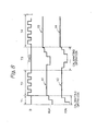
As illustrated in Fig. 4, which is a detailed
circuit diagram of the main-buffer circuit 2 (the dummy
main-buffer circuit 33) of Fig. 1, the main-buffer circuit
2 (the dummy main-buffer circuit 33) is constructed by
n- stage drivers 21, 22, ···, 2n each receiving one of the
pull-up signals P1, P2, ···, Pn (P1', P2', ... , Pn') and one
of the pull-down signals N1, N2, ···, Nn (N1', N2', ... , Nn')
from the pre-drivers 11, 12, ··· , in. In more detail, the
driver 2i (i = 1, 2, ···, n) is constructed by a p-channel
MOS transistor 201 and an N-chanael MOS transistor 202
connected in series powered by the high power supply voltage
VDD and the ground voltage GND.
For example, as illustrated in Fig. 5, when the
pull-up signal Pi (Pi') is low (activating level) and the
pull-down signal Ni is low (deactivating level), the
transistors 201 and 202 are turned ON and OFF, respectively,
so that the voltage at the output terminal OUT is high, On
the other hand, when the pull-up .signal Pi i (Pi') is high
(deactivating level) and the pull-down signal Ni is high
(activating level), the transistors 201 and 202 arc turned
OFF and ON, respectively, so that the voltage at the output
terminal OUT is low. Note that the pull-up signal Pi (Pi')
and the pull-down signal Ni (Ni') are never at the activating
levels simultaneously, i.e., which is forbidden. Also, when
the pull-up signal Pi (Pi') is high (deactivating level) and
the pull-down Ni (Ni') is low (activating level), the output
terminal OUT is in a high impedance (HZ) state.
The number n of the stages of the pre-drivers 11,
12,···, 1n, i.e., the drivers 21, 22, ···, 2n is predetermined
to cover the range of the characteristic impedance of the
transmission fluctuated by external conditions such as the
environmental temperature and the external power supply
voltages.
The calibrating operation of the impedance
adjusting circuit 3 of Fig. 1 will be explained next with
reference to Figs. 6, 7A and 7B. Here, impedance codes RUP,
RDN, RUP' and RDN' are defined by
RUP = (RUPn, RUPn-1, ... , RUP1)
RDN = (RDNn, loin-1, ... , PDN1)
RUP' = (RUPn', RUPn-1', ... , RUP1')
RDN' = (RDNn', RDNn-1', ···, PDN1')
The flowchart of Fig. 6 is carried out by the
control circuit 31.
First, at step 601, the dummy data D' is made "0"
(low). Then, at step 602, the switch 36 is turned ON while
the switch 35 is turned OFF, thus carrying out a calibrating
operation of the impedance code RUP. That is, at step 603,
the impedance code RUP' is initialized at 1. Then, at step
604, it is determined whether or not V2 = "1" where V2 is the
output signal of the comparator 34, i.e., whether or not the
output voltage V1 of the dummy main-buffer circuit 33 is
higher than a predetermined value such as VDD/2. The
operation at step 604 is repeated by steps 605 and 606 until
V2 = "1" is satisfied. Note that step 606 waits a
predetermined time. After V2 = "1" is satisfied, the control
proceeds to step 607 which renews the impedance code RUP with
RUP' (RUP = RUP') as shown in Fig. 7A, and at step 607, the
impedance code RUP is generated and transmitted to the
pre-buffer circuit 1.
Next, at step 609, the dummy data D' is made "0"
(low). Then, at step 610, the switch 35 is turned ON while
the switch 36 is turned OFF, thus carrying out a calibrating
operation of the impedance code RDN. That is, at step 611,
the impedance code RDN' is initialized at 1. Then, at step
612, it is determined whether or not V2 = "1", i.e., whether
or not the output voltage V1 of the dummy main-buffer circuit
33 is higher than a predetermined value such as VDD/2. The
operation at step 612 is repeated by steps 613 and 614 until
V2 = "1" is satisfied. Note that step 614 waits a
predetermined time. After V2 = "1" is satisfied, the control
proceeds to step 615 which renews the impedance code RDN with
RDN' (RDN = RDN') as shown in Fig. 7B, and at step 616, the
impedance code RDN is generated and transmitted to the
pre-buffer circuit 1.
In the calibrating operation as illustrated in
Figs. 6, 7A and 7B, however, the calibrating operation is
always carried out, i.e., the impedance codes RUP and EDN
are renewed and fetched by the pre-buffer circuit 1 in
synchronization with the data reading operation of the
pre-buffer circuit 1 and the main-buffer circuit 2, so that
the output signal at the output terminal OUT may be changed
in the middle of data "1" or "0", i.e., the output signal
at the output terminal OUT is distorted, thus deteriorating
the quality of the output signal at the output terminal OUT.
In order to suppress the distortion of the output
signal at the output terminal OUT, as illustrated in Fig.
8, the calibrating operation of Fig. 6 can be carried out
only during an initializing operation mode period T1 and a
disabling operation mode period T3 where the data D is not
supplied. In this case, however, during normal operation
mode periods T2 and T4, the impedance codes RUP and RDN are
not renewed, i.e., the impedance codes RUP and RDN
immediately before the normal operation mode periods T2 and
T4 are held as indicated by X1, X2, X3 and X4 of Fig. 8. Note
that during the initializing operation mode period T1, the
data signal D is "0" (low), while, during the disabling
operation mode period T3, the data signal D is fixed at "0"
(low) or "1" (high). As a result, a discrepancy between the
output impedance of the output buffer apparatus and the
characteristic impedance of the transmission line may be
suppressed, which would suppress reflection noise at the
terminal of the transmission line.
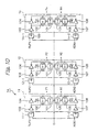
In Fig. 9, which illustrates a first embodiment
of the output buffer apparatus according to the present
invention, the pre-buffer circuit 1 of Fig. 1 is replaced
by a pre-buffer circuit 1A.
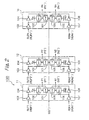
In Fig. 10, which is a detailed circuit diagram
of the pre-buffer circuit 1A of Fig. 9, D-type flip-flops
11-1, 11-2, 12-1, 12-2, ..., 1n-1, 1n-2 are added to the
elements of the pre-buffer circuit 1 of Fig. 2.
The D-type flip-flop 1i-1 (i = 1, 2, ···, n) has
a data input D for receiving the pull-up impedance adjusting
signal RUPi, a clock terminal C for receiving the data signal
D and an output terminal Q for generating an output signal
which is transmitted to the inverter 103 of the pre-driver
1i. That is, the pull-up impedance adjusting signal PUPi is
fetched by the D-type flip-flop 1i - 1 in synchronization with
a falling edge of the data signal D.
The D-type flip-flop 1i-2 (i = 1, 2, ..., n) has
a data input D for receiving the pull-down impedance
adjusting signal RDNi, a clock terminal C for receiving an
inverted signal of the data signal D and an output terminal
Q for generating an output signal which is transmitted to
the inverter 105 of the pre-driver 1i. That is, the pull-down
impedance adjusting signal PDNi is fetched by the D-type
flip-flop 1i-2 in synchronization with a rising edge of the
data signal D.
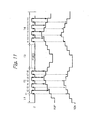
The operation of the output buffer apparatus of
Fig. 9 will be explained next with reference to Fig. 11,
where the impedance codes RUP and RDN are always renewed by
the flowchart of Fig. 6 and the graphs of Figs. 7A and 7B,
even during the initializing operation period T1 and the
disabling operation period T3.
That is, the impedance code RUP is fetched at
times t2, t4, t6, t8, 110, t12, t14, t16 by the falling edges
of the data signal D. On the other hand, the impedance code
RDN is fetched at times t1, t3, t5, t7, t9, t11, t13, t15
by the rising edges of the data signal D.
In the calibrating operation as illustrated in
Fig. 11, since the calibrating operation is always carried
out, the impedance codes RUP and RDN are renewed and fetched
by the pre-buffer circuit 1 in synchronization with the data
reading operation of the pre-buffer circuit 1 and the
main-buffer circuit 2, so that the output signal at the
output terminal OUT may be not changed in the middle of data
"1" or "0", i.e., the output signal at the output terminal
OUT is not distorted, thus improving the quality of the
output signal at the output terminal OUT. Also, during the
normal operation mode periods T2 and T4 since the impedance
codes RUP and RDN are renewed, i.e., a discrepancy between
the output impedance of the output buffer apparatus and the
characteristic impedance of the transmission line may not
be created, which would suppress reflection noise at the
terminal of the transmission line.
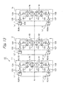
In Fig. 12, which illustrates a second embodiment
of the output buffer apparatus according to the present
invention, the pre-buffer circuit 1A of Fig. 9 is replaced
by a pre-buffer circuit 1B.
In Fig. 13, which is a detailed circuit diagram
of the pre-buffer circuit 1B of Fig. 12, latch circuits 11'-1,
11'-2, 12'-1, 12'-2, ... , 1n'-1, 1n'-2 are provided instead of
the D-type flip-flops 11-1, 11-2, 12-1, 12-2, 1n-1, 1n-2,
respectively, of Fig. 10.
The latch circuit 1i'-1 (i = 1, 2, ... , n) is
illustrated in detail in Fig. 14A. That is, the latch circuit
1i'-1 is constructed by inverters 1401 and 1402 for
receiving the data signal D to generate clock signals C1 and
its inverted signal, an inverter 1403 for receiving the
pull-up impedance adjusting signal RUPi, a transfer gate
1404, inverters 1405 and 1406, a transfer gate 1407, and a
buffer 1408 for generating a signal at an output terminal
Q.
The operation of the latch circuit 1i'-1(i = 1,
2, ..., n) is explained next with reference to Fig. 14B. That
is, when the data signal D is "0" (low), the transfer gates
1404 and 1407 are turned OFF and ON, respectively, so that
the latch circuit 1i'-1 is in a hold state. Therefore, the
signal at the output terminal Q is the same as the pull-up
impedance adjusting signal PUPi immediately before the data
signal D is switched from "1" (high) to "0" (low). On the
other hand, when the data signal D is "1" (high), the
transfer gates 1404 and 1407 are turned ON and OFF,
respectively, so that the latch circuit 1i'-1 is in a through
state. Therefore, the signal at the output terminal Q is
always the same as the pull-up impedance adjusting signal
PUPi.
The latch circuit 1i'-2 (i = 1, 2, ···, n) is
illustrated in detail in Fig. 15A. That is, the latch circuit
1i'-2 is constructed by inverters 1411 and 1412 for
receiving the data signal D to generate clock signals C2 and
its inverted signal, an inverter 1413 for receiving the
pull-down impedance adjusting signal RDNi, a transfer gate
1414, inverters 1415 and 1416, a transfer gate 1417, and a
buffer 1418 for generating a signal at an output terminal
Q.
The operation of the latch circuit 1i'-2(i = 1,
2,··· , n) is explained next with reference to Fig. 15B. That
is, when the data signal D is "0" (low), the transfer gates
1414 and 1417 are turned 0 and OFF, respectively, so that
the latch circuit 1i'-2 is in a through state. Therefore,
the signal at the output terminal Q is always the same as
the pull-down impedance adjusting signal PDNi. On the other
hand, when the data signal D is "1" (high), the transfer
gates 1414 and 1417 are turned OFF and ON, respectively, so
that the latch circuit 1i'-1 is in a hold state. Therefore,
the signal at the output terminal Q is the same as the
pull-down impedance adjusting signal PDNi immediately
before the data signal D is switched from "1" (low) to "0"
(low).
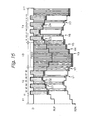
The operation of the output buffer apparatus of
Fig. 13 will be explained next with reference to Fig. 16,
where the impedance codes RUP and RDN are always renewed by
the flowchart of Fig. 6 and the graphs of Figs. 7A and 7B,
even during the initializing operation period T1 and the
disabling operation period T3 . Also, assume that the data
signal D is fixed at "0" (low) during the disabling operation
mode T3.
That is, the impedance code RUP is fetched at
periods t2 to t3, t4 to t5, t6 to t7, t8 to t8', t10 to t11,
t12 to t13, t14 to t15, t16 to t17 when the data signal D
is "0" (low). On the other hand, the impedance code RDP is
fetched at periods t1 to t2, t3 to t4, t5 to t6, t7 to t8,
t9 to t10 t11 to t12 t13 to t14, t15 to t16 when the data
signal D is "1" (high).
In the calibrating operation as illustrated in
Fig. 16, when the impedance code RUN is changed as indicated
by Y1, Y2, ··· in Fig. 16 while the data signal D continues
at the value "0" (low), the changed code RUN is fetched, and
also, when the impedance code RDP is changed as indicated
by Z1, Z2, ··· in Fig. 16 while the data signal D continues
at the value "1" (high), the changed code RDP is fetched.
Therefore, a discrepancy between the output impedance of the
output buffer apparatus and the characteristic impedance of
the transmission line may be suppressed which would suppress
reflection noise at the terminal of the transmission line.
As explained hereinabove, according to the
present invention, the quality of the output signal can be
improved, and also, reflection noise at a terminal of a
transmission line connected to the output buffer apparatus
can be suppressed.