EP1387607A1 - Module connector - Google Patents
Module connector Download PDFInfo
- Publication number
- EP1387607A1 EP1387607A1 EP03017380A EP03017380A EP1387607A1 EP 1387607 A1 EP1387607 A1 EP 1387607A1 EP 03017380 A EP03017380 A EP 03017380A EP 03017380 A EP03017380 A EP 03017380A EP 1387607 A1 EP1387607 A1 EP 1387607A1
- Authority
- EP
- European Patent Office
- Prior art keywords
- module body
- connector
- contact
- terminal
- chamber
- Prior art date
- Legal status (The legal status is an assumption and is not a legal conclusion. Google has not performed a legal analysis and makes no representation as to the accuracy of the status listed.)
- Withdrawn
Links
Images


Classifications
-
- H—ELECTRICITY
- H01—ELECTRIC ELEMENTS
- H01R—ELECTRICALLY-CONDUCTIVE CONNECTIONS; STRUCTURAL ASSOCIATIONS OF A PLURALITY OF MUTUALLY-INSULATED ELECTRICAL CONNECTING ELEMENTS; COUPLING DEVICES; CURRENT COLLECTORS
- H01R13/00—Details of coupling devices of the kinds covered by groups H01R12/70 or H01R24/00 - H01R33/00
- H01R13/46—Bases; Cases
- H01R13/514—Bases; Cases composed as a modular blocks or assembly, i.e. composed of co-operating parts provided with contact members or holding contact members between them
-
- H—ELECTRICITY
- H01—ELECTRIC ELEMENTS
- H01R—ELECTRICALLY-CONDUCTIVE CONNECTIONS; STRUCTURAL ASSOCIATIONS OF A PLURALITY OF MUTUALLY-INSULATED ELECTRICAL CONNECTING ELEMENTS; COUPLING DEVICES; CURRENT COLLECTORS
- H01R13/00—Details of coupling devices of the kinds covered by groups H01R12/70 or H01R24/00 - H01R33/00
- H01R13/648—Protective earth or shield arrangements on coupling devices, e.g. anti-static shielding
- H01R13/6485—Electrostatic discharge protection
-
- H—ELECTRICITY
- H04—ELECTRIC COMMUNICATION TECHNIQUE
- H04N—PICTORIAL COMMUNICATION, e.g. TELEVISION
- H04N23/00—Cameras or camera modules comprising electronic image sensors; Control thereof
- H04N23/50—Constructional details
- H04N23/54—Mounting of pick-up tubes, electronic image sensors, deviation or focusing coils
-
- H—ELECTRICITY
- H04—ELECTRIC COMMUNICATION TECHNIQUE
- H04N—PICTORIAL COMMUNICATION, e.g. TELEVISION
- H04N23/00—Cameras or camera modules comprising electronic image sensors; Control thereof
- H04N23/57—Mechanical or electrical details of cameras or camera modules specially adapted for being embedded in other devices
Definitions
- This invention relates to a connector to which a module body such as a memory module and a camera module is fitted.
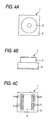
- Figs. 4A to 4C show a related-art camera module 1 to be mounted on a cellular mobile phone or the like, and this camera module 1 comprises a module body 2, and a lens portion 3 formed on an upper side of the module body 2. Two (left and right) rows of contact pads 4 and 5 are formed on a bottom face of the module body 2.
- Figs. 5A to 5C show a related-art connector 6 to which the camera module 1 is fitted.
- the connector 6 is formed into a square box-like body having an upwardly-open chamber 6a.
- Two (left and right) rows of parallel grooves 7 and 8 are formed in an upper face of a bottom 6b of the chamber 6a, so that the left grooves 7 extend from a central portion of the bottom 6b to an inner left side wall of the chamber 6a, and the right grooves 8 extend from the central portion of the bottom 6b to an inner right side wall of the chamber 6a.
- a row of left contact pins 9 are provided in the left grooves 7, respectively, while a row of right contact pins 10 are provided in the right grooves 8, respectively.
- each of the left row of contact pins 9 is bent upwardly to project from an associated groove 7 to form a contact projection 9a for contact with an associated contact pad 4 of the camera module 1.
- Each contact pin 9 extends left, and passes through the connector 6 to project to the exterior, and an outer end portion of the contact pin 9 is bent to form a terminal 9b for contact with a wiring board (not shown) on which the connector 6 is mounted.
- each of the right row of contact pins 10 is bent upwardly to project from an associated groove 7 to form a contact projection 10a for contact with an associated contact pad 5 of the camera module 1.
- Each contact pin 10 extends right, and passes through the connector 6 to project to the exterior, and an outer end portion of the contact pin 10 is bent to form a terminal 10b for contact with the wiring board.
- the contact pins 9 and 10 are bent as indicated in phantom lines in Fig. 6, so that the distal ends (inner ends) of the contact pins 9 and 10 abut against the bottom of the grooves 7 and 8.
- the contact pins 9 and 10 are accordingly held in firm press-contact respectively with the contact pads 4 and 5 because of reaction forces of these contact pins.
- Signals of the camera module 1 are transmitted to the contact pins 9 and 10 via the contact pads 4 and 5 and the contact projections 9a and 10a, and further are transmitted to a circuit (not shown) of the wiring board via the terminals 9b and 10b.
- the contact projections 9a and 10a of the contact pins 9 and 10 of the connector 6 are simultaneously brought into contact with the contact pads 4 and 5 of the camera module 1. Since it is not provided a measure for removing static electricity, there is an anxiety that the camera module 1 or an electric circuit connected to the connector 6 is damaged by static electricity.
- a connector to which a module body is electrically connected, comprising:
- the static electricity on the module body is removed when the conductive member of the module body is brought into contact with the grounding terminal, so that damage due to the static electricity is prevented.
- the chamber has a rectangular cross section when viewed from the opening; and the first terminal and the second terminal are provided on each of four inner side faces defining the chamber.
- the conductive member of the module body may be brought into contact with any one of the ground terminals provided respectively at the four inner side faces. Therefore, the static electricity can be surely removed.
- the second terminal is provided at a portion closer to the opening than the first terminal, so that the conductive member of the module body is first brought into contact with the second terminal when the module body is inserted into the chamber.
- the second terminal is formed with a protrusion which engages with the module body in a case where the module body is plenarily accommodated in the chamber.
- the module body can be retained against withdrawal with the simple construction.
- the first terminal and the second terminal are extended in a direction parallel to an inserting direction of the module body.
- the module body is a camera module.
- Figs. 1A to 1D show a camera module 21 mounted on a cellular mobile phone or the like, and this camera module 21 comprises a module body 22, and a lens portion 23 formed on an upper side of the module body 22.
- a plurality of parallel contact pads 24 are formed at a lower half portion of each of four side faces of the module body 22, and extend vertically.
- a recess 22a is formed in each of the four side faces of the module body 22 at an upper edge portion thereof, and extends vertically.
- FIGs. 2A to 2D show a connector 25 to which the camera module 21 is fitted.
- This connector 25 is formed into a square box-like body having an upwardly-open chamber 25a.
- Four side portions of a bottom 25b of the chamber 25a are suitably notched to form openings 25c, and a plurality of parallel contact pins 26 are provided on an inner side wall of the chamber 25a, and extend vertically.
- a ground terminal 27 for grounding purposes is provided on each inner side wall of the chamber 25a while being adjacent to each corner of the chamber 25a.
- Each ground terminal 27 is spaced a predetermined distance from the group of contact pins 26, and extended vertically.
- the four ground terminals 27 are so provided as to be opposed respectively to the four recesses 22a so that these ground terminals 27 can be engaged in the recesses 22a, respectively.
- Each of the contact pins 26 is bent into a generally inverted V-shape, and is fixedly secured to the inner side face of the chamber 25a.
- One end portion of the contact pin 26 is formed into a terminal 26a which is exposed to the lower side of the connector 25 through the associated opening 25c, and is bent outwardly horizontally so as to be electrically connected with a circuit (not shown) formed on a wiring board (not shown) on which the connector 25 is mounted.
- the other end portion of the contact pin 26 is bent to project inwardly to form a contact projection 26b for contact with the associated contact pad 24 of the module body 22.
- Each of the ground terminals 27 is bent into a generally U-shape, and one end of the ground terminal 27 is fixedly secured to the inner side face of the chamber 25a. That portion of the ground terminal 27, disposed adjacent to the other end (upper end) thereof, is bent to project toward the chamber 25a to form a contact projection 27a.
- the contact projection 27a is disposed at a level above the contact projections 26b of the contact pins 26.
- the contact pads 24 are brought into press-contact with the contact projections 26b of the contact pins 26, while the contact projections 27a of the ground terminals 27 are engaged in the recesses 22a, respectively.
- the camera module 21 can be retained against withdrawal. The attachment of the camera module 21 to the connector 25 is thus completed.
- Signals of the camera module 21 are transmitted from the contact pads 24 to the contact pins 26 via the contact projections 26b, and further are transmitted to the circuit of the wiring board via the terminals 26a.
- the shape of the recesses 22a is not particularly limited, and these grooves may have any suitable shape in so far as the contact projections 27a can be engaged in the recesses 22a.
- the connector 25 is so designed as to attach the camera module 21 thereto
- the connector of the invention is not limited to the type for attaching the camera module thereto, but the invention can be applied to connectors for attaching various modules (such for example as a memory module) or electric parts thereto.
Abstract


Description
- This invention relates to a connector to which a module body such as a memory module and a camera module is fitted.
- Figs. 4A to 4C show a related-
art camera module 1 to be mounted on a cellular mobile phone or the like, and thiscamera module 1 comprises amodule body 2, and alens portion 3 formed on an upper side of themodule body 2. Two (left and right) rows ofcontact pads module body 2. - Figs. 5A to 5C show a related-
art connector 6 to which thecamera module 1 is fitted. Theconnector 6 is formed into a square box-like body having an upwardly-open chamber 6a. Two (left and right) rows ofparallel grooves bottom 6b of thechamber 6a, so that theleft grooves 7 extend from a central portion of thebottom 6b to an inner left side wall of thechamber 6a, and theright grooves 8 extend from the central portion of thebottom 6b to an inner right side wall of thechamber 6a. A row ofleft contact pins 9 are provided in theleft grooves 7, respectively, while a row ofright contact pins 10 are provided in theright grooves 8, respectively. - As shown in Fig. 6, an inner end portion of each of the left row of
contact pins 9 is bent upwardly to project from an associatedgroove 7 to form acontact projection 9a for contact with an associatedcontact pad 4 of thecamera module 1. Eachcontact pin 9 extends left, and passes through theconnector 6 to project to the exterior, and an outer end portion of thecontact pin 9 is bent to form aterminal 9b for contact with a wiring board (not shown) on which theconnector 6 is mounted. - Similarly, an inner end portion of each of the right row of
contact pins 10 is bent upwardly to project from an associatedgroove 7 to form acontact projection 10a for contact with an associatedcontact pad 5 of thecamera module 1. Eachcontact pin 10 extends right, and passes through theconnector 6 to project to the exterior, and an outer end portion of thecontact pin 10 is bent to form aterminal 10b for contact with the wiring board. - When the
contact projections contact pins contact pads camera module 1 from the upper side, thecontact pins contact pins grooves contact pins contact pads - When the
camera module 1 is inserted into thechamber 6a of theconnector 6 from the upper side of thisconnector 6, thecontact pads camera module 1 are press-contacted respectively with thecontact projections connector pins connector 6, as shown in Fig. 7. - Signals of the
camera module 1 are transmitted to thecontact pins contact pads contact projections terminals - In the above construction, however, the
contact projections contact pins connector 6 are simultaneously brought into contact with thecontact pads camera module 1. Since it is not provided a measure for removing static electricity, there is an anxiety that thecamera module 1 or an electric circuit connected to theconnector 6 is damaged by static electricity. - It is therefore an object of the invention to provide a module connector in which the static electricity on an attached module body can be surely removed to prevent damage due to the static electricity.
- In order to achieve the above object, according to the invention, there is provided a connector, to which a module body is electrically connected, comprising:
- a connector body, having an inner side face defining a chamber which accommodates the module body, the chamber formed with an opening from which the module body is inserted;
- a first, conductive terminal, provided on the inner side face such that a conductive member formed on an outer periphery of the module body is brought into contact with the first terminal in a case where the module body is plenarily accommodated in the chamber; and
- a second, grounding terminal, provided on the inner side face and operable to be brought into contact with the conductive member of the module body.
-
- With such a configuration, the static electricity on the module body is removed when the conductive member of the module body is brought into contact with the grounding terminal, so that damage due to the static electricity is prevented.
- It is preferable that: the chamber has a rectangular cross section when viewed from the opening; and the first terminal and the second terminal are provided on each of four inner side faces defining the chamber.
- With such a configuration, the conductive member of the module body may be brought into contact with any one of the ground terminals provided respectively at the four inner side faces. Therefore, the static electricity can be surely removed.
- Preferably, the second terminal is provided at a portion closer to the opening than the first terminal, so that the conductive member of the module body is first brought into contact with the second terminal when the module body is inserted into the chamber.
- With such a configuration, the static electricity can be removed more safely.
- Here, it is preferable that the second terminal is formed with a protrusion which engages with the module body in a case where the module body is plenarily accommodated in the chamber.
- With such a configuration, the module body can be retained against withdrawal with the simple construction.
- Preferably, the first terminal and the second terminal are extended in a direction parallel to an inserting direction of the module body.
- Preferably, the module body is a camera module.
- The above objects and advantages of the present invention will become more apparent by describing in detail preferred exemplary embodiments thereof with reference to the accompanying drawings, wherein:
- Fig. 1A is a top plan view of a camera module according to one embodiment of the invention;
- Fig. 1B is a side view of the camera module;
- Fig. 1C is a partly sectional front view of the camera module;
- Fig. 1D is a bottom plan view of the camera module;
- Fig. 2A is a top plan view of a connector according to one embodiment of the invention;
- Fig. 2B is a side view of the connector;
- Fig. 2C is a front view of the connector;
- Fig. 2D is a sectional front view of the connector;
- Fig. 3 is a partly sectional front view showing a state that the camera module is fitted with the connector;
- Fig. 4A is a top plan view of a related-art camera module;
- Fig. 4B is a side view of the related-art camera module;
- Fig. 4C is a bottom plan view of the related-art camera module;
- Fig. 5A is a top plan view of a related-art connector;
- Fig. 5B is a front view of the related-art connector;
- Fig. 5C is a side view of the related-art connector;
- Fig. 6 is a sectional front view of the related-art connector; and
- Fig. 7 is a partly sectional front view showing a state that the related-art camera module is fitted with the related-art connector.
-
- One preferred embodiment of the present invention will now be described in detail with reference to the accompanying drawings.
- Figs. 1A to 1D show a
camera module 21 mounted on a cellular mobile phone or the like, and thiscamera module 21 comprises amodule body 22, and alens portion 23 formed on an upper side of themodule body 22. A plurality of parallel contact pads 24are formed at a lower half portion of each of four side faces of themodule body 22, and extend vertically. - A
recess 22a is formed in each of the four side faces of themodule body 22 at an upper edge portion thereof, and extends vertically. - Figs. 2A to 2D show a
connector 25 to which thecamera module 21 is fitted. Thisconnector 25 is formed into a square box-like body having an upwardly-open chamber 25a. Four side portions of a bottom 25b of thechamber 25a are suitably notched to formopenings 25c, and a plurality of parallel contact pins 26 are provided on an inner side wall of thechamber 25a, and extend vertically. - A
ground terminal 27 for grounding purposes is provided on each inner side wall of thechamber 25a while being adjacent to each corner of thechamber 25a. Eachground terminal 27 is spaced a predetermined distance from the group of contact pins 26, and extended vertically. The fourground terminals 27 are so provided as to be opposed respectively to the fourrecesses 22a so that theseground terminals 27 can be engaged in therecesses 22a, respectively. - Each of the contact pins 26 is bent into a generally inverted V-shape, and is fixedly secured to the inner side face of the
chamber 25a. One end portion of thecontact pin 26 is formed into a terminal 26a which is exposed to the lower side of theconnector 25 through the associatedopening 25c, and is bent outwardly horizontally so as to be electrically connected with a circuit (not shown) formed on a wiring board (not shown) on which theconnector 25 is mounted. The other end portion of thecontact pin 26 is bent to project inwardly to form acontact projection 26b for contact with the associatedcontact pad 24 of themodule body 22. - Each of the
ground terminals 27 is bent into a generally U-shape, and one end of theground terminal 27 is fixedly secured to the inner side face of thechamber 25a. That portion of theground terminal 27, disposed adjacent to the other end (upper end) thereof, is bent to project toward thechamber 25a to form acontact projection 27a. Thecontact projection 27a is disposed at a level above thecontact projections 26b of the contact pins 26. - When the
camera module 21 is inserted into thechamber 25a from the upper side of thisconnector 25, one of thecontact pads 24 of thecamera module 21 is first brought into contact with thecontact projection 27a of an associated one of theground terminals 27 provided on the inner side face of thechamber 25b, thereby positively removing static electricity of thecamera module 21. Therefore, damage due to the static electricity can be prevented. - Then, the
contact pads 24 are brought into press-contact with thecontact projections 26b of the contact pins 26, while thecontact projections 27a of theground terminals 27 are engaged in therecesses 22a, respectively. With this simple structure, thecamera module 21 can be retained against withdrawal. The attachment of thecamera module 21 to theconnector 25 is thus completed. - Signals of the
camera module 21 are transmitted from thecontact pads 24 to the contact pins 26 via thecontact projections 26b, and further are transmitted to the circuit of the wiring board via theterminals 26a. - In the present invention, various modifications can be made without departing from the spirits of the invention, and such modifications fall within the scope of the invention.
- For example, the shape of the
recesses 22a is not particularly limited, and these grooves may have any suitable shape in so far as thecontact projections 27a can be engaged in therecesses 22a. Alternatively, there may be provided a construction in which thecontact projections 27a can be engaged with the upper face of themodule body 22. - Although the
connector 25 is so designed as to attach thecamera module 21 thereto, the connector of the invention is not limited to the type for attaching the camera module thereto, but the invention can be applied to connectors for attaching various modules (such for example as a memory module) or electric parts thereto.
Claims (6)
- A connector, to which a module body is electrically connected, comprising:a connector body, having an inner side face defining a chamber which accommodates the module body, the chamber formed with an opening from which the module body is inserted;a first, conductive terminal, provided on the inner side face such that a conductive member formed on an outer periphery of the module body is brought into contact with the first terminal in a case where the module body is plenarily accommodated in the chamber; anda second, grounding terminal, provided on the inner side face and operable to be brought into contact with the conductive member of the module body.
- The connector as set forth in claim 1, wherein:the chamber has a rectangular cross section when viewed from the opening; andthe first terminal and the second terminal are provided on each of four inner side faces defining the chamber.
- The connector as set forth in claim 1, wherein the second terminal is provided at a portion closer to the opening than the first terminal, so that the conductive member of the module body is first brought into contact with the second terminal when the module body is inserted into the chamber.
- The connector as set forth in claim 3, wherein the second terminal is formed with a protrusion which engages with the module body in a case where the module body is plenarily accommodated in the chamber.
- The connector as set forth in claim 1, wherein the first terminal and the second terminal are extended in a direction parallel to an inserting direction of the module body.
- The connector as set forth in claim 1, wherein the module body is a camera module.
Applications Claiming Priority (2)
| Application Number | Priority Date | Filing Date | Title |
|---|---|---|---|
| JP2002224127 | 2002-07-31 | ||
| JP2002224127A JP2004063425A (en) | 2002-07-31 | 2002-07-31 | Connector for module |
Publications (1)
| Publication Number | Publication Date |
|---|---|
| EP1387607A1 true EP1387607A1 (en) | 2004-02-04 |
Family
ID=30112974
Family Applications (1)
| Application Number | Title | Priority Date | Filing Date |
|---|---|---|---|
| EP03017380A Withdrawn EP1387607A1 (en) | 2002-07-31 | 2003-07-31 | Module connector |
Country Status (4)
| Country | Link |
|---|---|
| US (1) | US6905344B2 (en) |
| EP (1) | EP1387607A1 (en) |
| JP (1) | JP2004063425A (en) |
| KR (1) | KR100835264B1 (en) |
Cited By (9)
| Publication number | Priority date | Publication date | Assignee | Title |
|---|---|---|---|---|
| EP1471731A2 (en) * | 2003-03-31 | 2004-10-27 | Mitsumi Electric Co., Ltd. | Mounting structure for compact camera module |
| FR2869460A1 (en) * | 2004-04-23 | 2005-10-28 | Premier Image Technology Corp | LENS MODULE AND METHOD OF ASSEMBLING THE SAME |
| EP1622362A1 (en) * | 2004-07-12 | 2006-02-01 | Research In Motion Limited | Structure for mounting a component to a circuit-board |
| WO2006042133A1 (en) * | 2004-10-07 | 2006-04-20 | Molex Incorporated | Socket for digital camera module |
| US7697275B2 (en) | 2004-09-03 | 2010-04-13 | Research In Motion Limited | Shock resistant mounting for small display screen |
| US7699619B2 (en) | 2005-01-31 | 2010-04-20 | Molex Incorporated | Socket for camera module |
| US7918671B2 (en) | 2004-07-13 | 2011-04-05 | Research In Motion Limited | Mounting structure with springs biasing towards a latching edge |
| EP2394426A1 (en) * | 2009-02-06 | 2011-12-14 | Magna Electronics Inc. | Improvements to camera for vehicle |
| CN102904120A (en) * | 2011-07-13 | 2013-01-30 | 泰科电子公司 | Grounding structures for header and receptacle assemblies |
Families Citing this family (26)
| Publication number | Priority date | Publication date | Assignee | Title |
|---|---|---|---|---|
| JP4919243B2 (en) * | 2002-04-11 | 2012-04-18 | 奇美電子股▲ふん▼有限公司 | Electrical insulator and electronic device |
| JP3956920B2 (en) * | 2003-08-26 | 2007-08-08 | 松下電工株式会社 | connector |
| JP2005222876A (en) | 2004-02-09 | 2005-08-18 | Smk Corp | Connector for module |
| JP3979408B2 (en) * | 2004-08-30 | 2007-09-19 | ミツミ電機株式会社 | Connector locking device for camera module |
| JP2006079871A (en) * | 2004-09-08 | 2006-03-23 | Smk Corp | Socket for electronic module |
| CN2749141Y (en) * | 2004-10-25 | 2005-12-28 | 富士康(昆山)电脑接插件有限公司 | Electric connector |
| JP4091593B2 (en) * | 2004-11-05 | 2008-05-28 | Smk株式会社 | Connection structure of camera module with autofocus function and module connector |
| TWM271287U (en) * | 2005-02-18 | 2005-07-21 | Molex Taiwan Ltd | Camera module connector |
| US20060189216A1 (en) * | 2005-02-18 | 2006-08-24 | Ming-Hsun Yang | Camera module connector keying structure |
| US7077664B1 (en) * | 2005-03-08 | 2006-07-18 | Cheng Uei Precision Industry Co., Ltd. | Module connector |
| CN2809968Y (en) * | 2005-05-31 | 2006-08-23 | 富士康(昆山)电脑接插件有限公司 | Electric connector |
| CN2800590Y (en) * | 2005-05-31 | 2006-07-26 | 富士康(昆山)电脑接插件有限公司 | Electric connector |
| JP2007123214A (en) * | 2005-10-31 | 2007-05-17 | Mitsumi Electric Co Ltd | Mounting structure of camera module |
| JP4359591B2 (en) * | 2005-12-26 | 2009-11-04 | アルプス電気株式会社 | The camera module |
| TWM304793U (en) * | 2006-04-03 | 2007-01-11 | Hon Hai Prec Ind Co Ltd | Electrical connector assembly |
| KR101231305B1 (en) * | 2006-05-25 | 2013-02-07 | 엘지이노텍 주식회사 | camera module assembly |
| TWM310502U (en) * | 2006-11-17 | 2007-04-21 | Molex Taiwan Ltd | Electrical connection device |
| JP2008311149A (en) * | 2007-06-15 | 2008-12-25 | Mitsumi Electric Co Ltd | Module connector |
| KR100876109B1 (en) | 2007-09-11 | 2008-12-26 | 삼성전기주식회사 | Camera module and manufacturing method thereof |
| JP4924973B2 (en) * | 2009-02-24 | 2012-04-25 | Smk株式会社 | Camera module socket |
| KR101018154B1 (en) | 2009-04-10 | 2011-02-28 | 삼성전기주식회사 | Camera Module Package |
| KR101008447B1 (en) * | 2009-10-06 | 2011-01-14 | 삼성전기주식회사 | Camera module |
| KR101060951B1 (en) * | 2009-10-23 | 2011-08-30 | 삼성전기주식회사 | Camera module package |
| KR101125077B1 (en) * | 2010-04-28 | 2012-03-21 | 삼성전기주식회사 | Mobile apparatus |
| JP4999020B2 (en) * | 2010-06-28 | 2012-08-15 | Smk株式会社 | Connector device |
| KR20210046549A (en) | 2019-10-18 | 2021-04-28 | 미쓰미덴기가부시기가이샤 | Electrical connector and electronic device |
Citations (4)
| Publication number | Priority date | Publication date | Assignee | Title |
|---|---|---|---|---|
| US4739356A (en) * | 1986-07-23 | 1988-04-19 | Canon Kabushiki Kaisha | Electric connector for camera |
| US5073117A (en) * | 1989-03-30 | 1991-12-17 | Texas Instruments Incorporated | Flip-chip test socket adaptor and method |
| EP1148716A1 (en) * | 2000-04-07 | 2001-10-24 | Mitsubishi Denki Kabushiki Kaisha | Imaging device |
| EP1213924A1 (en) * | 2000-11-30 | 2002-06-12 | Mitsubishi Denki Kabushiki Kaisha | Portable telephone provided with image pickup device |
Family Cites Families (3)
| Publication number | Priority date | Publication date | Assignee | Title |
|---|---|---|---|---|
| EP0404277B1 (en) * | 1984-02-27 | 1994-09-28 | The Whitaker Corporation | Method of inserting a chip carrier contact into a housing |
| EP0532166B1 (en) * | 1991-09-11 | 1995-06-14 | ITT INDUSTRIES, INC. (a Delaware corporation) | Memory card grounding apparatus |
| US6328574B1 (en) * | 2001-07-27 | 2001-12-11 | Hon Hai Precision Ind. Co., Ltd. | High current capacity socket with side contacts |
-
2002
- 2002-07-31 JP JP2002224127A patent/JP2004063425A/en active Pending
-
2003
- 2003-07-29 KR KR1020030052267A patent/KR100835264B1/en not_active IP Right Cessation
- 2003-07-29 US US10/628,331 patent/US6905344B2/en not_active Expired - Fee Related
- 2003-07-31 EP EP03017380A patent/EP1387607A1/en not_active Withdrawn
Patent Citations (4)
| Publication number | Priority date | Publication date | Assignee | Title |
|---|---|---|---|---|
| US4739356A (en) * | 1986-07-23 | 1988-04-19 | Canon Kabushiki Kaisha | Electric connector for camera |
| US5073117A (en) * | 1989-03-30 | 1991-12-17 | Texas Instruments Incorporated | Flip-chip test socket adaptor and method |
| EP1148716A1 (en) * | 2000-04-07 | 2001-10-24 | Mitsubishi Denki Kabushiki Kaisha | Imaging device |
| EP1213924A1 (en) * | 2000-11-30 | 2002-06-12 | Mitsubishi Denki Kabushiki Kaisha | Portable telephone provided with image pickup device |
Cited By (22)
| Publication number | Priority date | Publication date | Assignee | Title |
|---|---|---|---|---|
| EP1471731A2 (en) * | 2003-03-31 | 2004-10-27 | Mitsumi Electric Co., Ltd. | Mounting structure for compact camera module |
| EP1471731A3 (en) * | 2003-03-31 | 2007-10-17 | Mitsumi Electric Co., Ltd. | Mounting structure for compact camera module |
| EP2018045A1 (en) * | 2003-03-31 | 2009-01-21 | Mitsumi Electric Co., Ltd. | Mounting Structure For Compact Camera Module |
| FR2869460A1 (en) * | 2004-04-23 | 2005-10-28 | Premier Image Technology Corp | LENS MODULE AND METHOD OF ASSEMBLING THE SAME |
| DE102004036143A1 (en) * | 2004-04-23 | 2005-11-17 | Premier Image Technology Corp. | Lens module and method of making the same |
| EP2134077A1 (en) * | 2004-07-12 | 2009-12-16 | Research In Motion Limited | Structure for mounting a camera unit to a circuit-board |
| EP1622362A1 (en) * | 2004-07-12 | 2006-02-01 | Research In Motion Limited | Structure for mounting a component to a circuit-board |
| US7918671B2 (en) | 2004-07-13 | 2011-04-05 | Research In Motion Limited | Mounting structure with springs biasing towards a latching edge |
| US7697275B2 (en) | 2004-09-03 | 2010-04-13 | Research In Motion Limited | Shock resistant mounting for small display screen |
| WO2006042133A1 (en) * | 2004-10-07 | 2006-04-20 | Molex Incorporated | Socket for digital camera module |
| US7699619B2 (en) | 2005-01-31 | 2010-04-20 | Molex Incorporated | Socket for camera module |
| US8866907B2 (en) | 2009-02-06 | 2014-10-21 | Magna Electronics Inc. | Camera for mounting on a vehicle |
| EP2394426A4 (en) * | 2009-02-06 | 2013-02-20 | Magna Electronics Inc | Improvements to camera for vehicle |
| EP2394426A1 (en) * | 2009-02-06 | 2011-12-14 | Magna Electronics Inc. | Improvements to camera for vehicle |
| US9346415B2 (en) | 2009-02-06 | 2016-05-24 | Magna Electronics Inc. | Camera for mounting on a vehicle |
| US10137843B2 (en) | 2009-02-06 | 2018-11-27 | Magna Electronics Inc. | Process for providing a camera for mounting on a vehicle |
| US10556555B2 (en) | 2009-02-06 | 2020-02-11 | Magna Electronics Inc. | Process for providing a vehicular camera |
| US10875470B2 (en) | 2009-02-06 | 2020-12-29 | Magna Electronics Inc. | Vehicular camera with locking attachment at vehicle panel |
| US11312315B2 (en) | 2009-02-06 | 2022-04-26 | Magna Electronics Inc. | Vehicular camera with electrical connectors that allow for misalignment |
| US11807171B2 (en) | 2009-02-06 | 2023-11-07 | Magna Electronics Inc. | Vehicular camera with electrical connectors that allow for misalignment |
| CN102904120A (en) * | 2011-07-13 | 2013-01-30 | 泰科电子公司 | Grounding structures for header and receptacle assemblies |
| CN102904120B (en) * | 2011-07-13 | 2016-05-11 | 泰科电子公司 | For the ground structure of plug and socket assembly |
Also Published As
| Publication number | Publication date |
|---|---|
| KR20040012516A (en) | 2004-02-11 |
| JP2004063425A (en) | 2004-02-26 |
| US20040023527A1 (en) | 2004-02-05 |
| US6905344B2 (en) | 2005-06-14 |
| KR100835264B1 (en) | 2008-06-05 |
Similar Documents
| Publication | Publication Date | Title |
|---|---|---|
| US6905344B2 (en) | Module connector | |
| US7163407B2 (en) | Module connector | |
| US6729890B2 (en) | Reduced-size board-to-board connector | |
| KR100224056B1 (en) | Electric connector assembly with an improved retention characteristics | |
| US6299484B2 (en) | Shielded connector | |
| US4695115A (en) | Telephone connector with bypass capacitor | |
| US4867690A (en) | Electrical connector system | |
| US5188535A (en) | Low profile electrical connector | |
| JP3150303U (en) | Electrical connector | |
| US20050112952A1 (en) | Power jack connector | |
| US6790054B1 (en) | Two-piece right angle contact edge card connector | |
| US20070155240A1 (en) | Electrical connector with firm frame for mating with corresponding connector | |
| KR20140099825A (en) | Electrical Connector Assembly and Electrical Connector therefore | |
| US6524130B1 (en) | Electrical connector assembly | |
| US7438601B2 (en) | Connector | |
| US6508665B1 (en) | Electrical connector having printed circuit board mounted therein | |
| US6688909B1 (en) | Stacked connector with leds | |
| US20110244734A1 (en) | Component-to-board electrical connector | |
| JP3898643B2 (en) | Small board to board connector | |
| US7572151B2 (en) | Plug connector for mobile communication device | |
| US20010003077A1 (en) | Shielded connector assembly | |
| US6905345B2 (en) | Electrical connector assembly | |
| US5722839A (en) | Electrical connector for horizontal insertion of a CPU module therein | |
| US6511352B2 (en) | Connector connection structure | |
| KR100806358B1 (en) | Connector plug for a mobile communication device |
Legal Events
| Date | Code | Title | Description |
|---|---|---|---|
| PUAI | Public reference made under article 153(3) epc to a published international application that has entered the european phase |
Free format text: ORIGINAL CODE: 0009012 |
|
| AK | Designated contracting states |
Kind code of ref document: A1 Designated state(s): AT BE BG CH CY CZ DE DK EE ES FI FR GB GR HU IE IT LI LU MC NL PT RO SE SI SK TR |
|
| AX | Request for extension of the european patent |
Extension state: AL LT LV MK |
|
| 17P | Request for examination filed |
Effective date: 20040728 |
|
| AKX | Designation fees paid |
Designated state(s): DE FR |
|
| 17Q | First examination report despatched |
Effective date: 20041004 |
|
| 17Q | First examination report despatched |
Effective date: 20041004 |
|
| STAA | Information on the status of an ep patent application or granted ep patent |
Free format text: STATUS: THE APPLICATION IS DEEMED TO BE WITHDRAWN |
|
| 18D | Application deemed to be withdrawn |
Effective date: 20110201 |