Technical Field:
-
The present invention relates to methods for manufacturing a silicon
wafer and a silicon epitaxial wafer capable of obtaining the silicon wafer and
the silicon epitaxial wafer having a defect-free layer (a DZ layer or an
epitaxial layer) in the vicinity of a surface thereof and oxide precipitates high
in gettering capability in the bulk thereof through heat treatment with
extreme efficiency and simplicity, and a silicon epitaxial wafer.
Background Art:
-
Most of silicon wafers used widely as substrates of semiconductor
devices are manufactured from a silicon single crystal grown in a Czochralski
(CZ) method. The silicon single crystal grown in the CZ method contains
interstitial oxygen as impurities at concentration of about 1018 atoms/cm3.
The interstitial oxygen turns into a supersatulated state in a thermal history
from solidification of a melt till cooling down thereof to room temperature
during a crystal growth step (hereinafter which may be referred to as a
crystal thermal history) or in a heat treatment step of a fabrication process of
semiconductor devices to then precipitate, precipitates of silicon oxides
(hereinafter may be referred to as oxide precipitates or simply precipitates)
being generated.
-
The oxide precipitates work effectively as sites capturing heavy
metal impurities contaminated in a device fabrication process. This is called
internal gettering (hereinafter may be referred to as IG or simply gettering)
and improves device characteristics and a yield. For this reason, an IG
capability is valued highly as one of properties of a silicon wafer.
-
The process of oxygen precipitation includes formation of
precipitation nuclei and their growth. Usually formation of nuclei progresses
during a crystal thermal history, and then the nuclei grow greatly in heat
treatment of the following device fabrication process and others, the grown
nuclei being detected as oxide precipitates. For this reason, the precipitation
nuclei generated during the crystal thermal history are referred to as
grown-in precipitation nuclei. As a matter of course, oxygen precipitation
nuclei may be generated in subsequent heat treatment.
-
A usual as-grown wafer (a wafer subjected to no heat treatment
except for general oxygen donor anihilation heat treatment) has no IG
capability because oxygen precipitation nuclei existing at a stage prior to a
device fabrication process are extremely small. However, after the as grown
wafer has been subjected to the device fabrication process, the nuclei grow to
large oxide precipitates and then the wafer has an IG capability.
-
Since density of oxygen precipitation nuclei generated during a
crystal thermal history depends on the length of the thermal history, there
arises a problem that the density is largely fluctuated according to crystal
pulling conditions such as a pulling rate or a position in the direction of a
crystal growth axis. For example, in a process producing one crystal, a
portion grown in a latter half thereof has lower density of oxygen
precipitation nuclei because of a shorter thermal history. This causes a
fluctuation in density of oxygen precipitation nuclei to be generated during a
device fabrication process, resulting in a fluctuation in an IG capability.
-
On the other hand, when oxide precipitates exist in a device
fabrication region in the vicinity of a wafer surface, degradation of the device
characteristics occurs. For this reason, in order to prevent progress in oxygen
precipitation by out-diffusing oxygen in the vicinity of the wafer surface, the
wafer may be heat-treated at 1100°C or higher for several hours. In this case,
most of grown-in precipitation nuclei are annihilated and thereby, oxide
precipitates are not generated in the following device fabrication process.
-
Therefore, in order to regenerate oxygen precipitation nuclei, the
wafer is subjected to heat treatment at about 650°C for a long time on the
order of 3 hrs to 30 hrs. Further, in order to grow the regenerated oxygen
precipitation nuclei into large oxide precipitates having an IG capability, the
wafer may be additionally subjected to heat treatment at about 1000°C.
There is generally called DZ-IG treatment a combination of the three types of
heat treatment, that is, the heat treatment out-diffusing oxygen residing in
the vicinity of the wafer surface, the heat treatment generating oxygen
precipitation nuclei in the interior of the wafer, and the heat treatment
growing the oxygen precipitation nuclei.
-
With the DZ-IG treatment, an ideal structure is formed in which
there are no oxide precipitates in the vicinity of a wafer surface to be a device
fabrication region, while there are generated oxide precipitates having an IG
capability in the interior thereof (hereinafter the structure may be referred to
as a DZ-IG structure). However, this treatment is long in the total process for
heat treatment, resulting in poor efficiency.
-
Also, a general CZ wafer contains void-like defects generated by
aggregation of atomic vacancies in addition to grown-in precipitation nuclei.
When the void defect is exposed on a surface of a mirror-polished wafer, they
are observed as surface pits called COP (crystal originated particle). When
the COPs and voids are present in the device fabrication region, degradation
of the device characteristics occurs too. For this reason, in order to eliminate
the COPs and voids in the vicinity of the wafer surface, the wafer may be
subjected to high-temperature heat treatment at a temperature of the order
of 1200°C or higher in hydrogen or argon atmosphere.
-
However, in this case, a problem arises that thermal stress causes
slip generation. In order to suppress slip generation, a temperature of heat
treatment is desirably lower, while at lower heat treatment temperatures,
the COPs and voids are harder to be eliminated.
-
Further, in this case as well, an IG capability is preferably to be
imparted. Then, as a method in which annihilation of the COPs and voids in
the vicinity of a wafer surface and generation of oxide precipitates in the
interior of the wafer are simultaneously realized, there has been known a
method in which nitrogen is added during crystal growth. In a wafer added
with nitrogen, smaller voids are easily annihilated by high-temperature heat
treatment, while larger grown-in precipitation nuclei grow without
annihilation even in high-temperature treatment into oxide precipitates,
thereby an IG capability being imparted.
-
However, even when a wafer added with nitrogen is used, there is no
change in that it is necessarily subjected to high-temperature heat treatment
at about 1200°C. As the wafer diameter becomes larger, the slip more easily
generates; therefore especially in a 300 mm wafer that is the mainstream
hereafter, there becomes a great problem need of high-temperature heat
treatment at about 1200°C or higher.
-
Further, since the area where void defects are annihilated is in a
very thin surface layer of the order of several µm from the surface, the void
defects may degrade device characteristics in a device using a surface layer
deeper than the very thin surface layer as a device fabrication region.
-
In order to bring a device fabrication region in the vicinity of a wafer
surface into a defect-free state, there may be used an epitaxial wafer
(hereinafter may be referred to as an epi wafer) that is manufactured by
depositing silicon single crystal on a silicon wafer as an epitaxial growth
substrate by means of vapor phase growth. In this epi wafer, it is also
important to impart an IG capability to the substrate.
-
However, since a usual epitaxial step (hereinafter may be referred to
as an epi step) is operated at a high-temperature of about 1100°C or higher,
most oxygen precipitation nuclei (grown-in precipitation nuclei) in the
substrate generated in a crystal thermal history are annihilated and thereby
no oxide precipitates are generated in the subsequent device fabrication
process. Accordingly, in an epi wafer, there arises a problem that an IG
capability deteriorates.
-
As a solution of this problem, there has been known a method in
which by performing heat treatment at about 800°C prior to an epi step,
grown-in precipitation nuclei generated in a crystal thermal history are
grown to sizes not to be annihilated even in a high-temperature epi step. In
this method, when a heat treatment temperature prior to epi growth is 800°C,
grown-in precipitation nuclei with sizes equal to or larger than a critical size
(the minimum size of a precipitation nucleus that can stably grow at the
temperature) at 800°C grow and survive during an epi step, and the survived
nuclei further grow into oxide precipitates in heat treatment such as a device
fabrication process after the epi step.
-
In general, density of small grown-in precipitation nuclei is higher,
while density of large grown-in precipitation nuclei is lower. Furthermore,
the lower the heat treatment temperature is, the smaller the critical size
becomes. Therefore, in order to generate grown-in precipitation nuclei at
higher density for imparting a more excellent IG capability, it is desirable to
lower the heat treatment temperature prior to the epi step. However, if the
heat treatment temperature is lowered, a growth rate of precipitation nuclei
is slowed, so a long time of heat treatment is required for growing the
precipitation nuclei to sizes not to be annihilated even in an epi step, which is
not preferable because of reduction in productivity.
-
Furthermore, if there exist oxide precipitates having sizes not to be
annihilated even in an epi step, in a recent device fabrication process having
a lower temperature and a shorter time, no further growth of the oxide
precipitates can be expected in heat treatment of the device fabrication
process. In order to exert a gettering capability in such a recent device
fabrication process, it is necessary to generate oxide precipitates with sizes
having a gettering capability at high density prior to the device fabrication
process.
-
As described above, in the recent device fabrication process, a trend
of a lower temperature and a shorter time in a device fabrication process has
progressed in company with the use of a larger-size wafer therein; for
example, a series of steps in the device fabrication process are all performed
at a temperature of 1000°C or lower, and RTP (rapid thermal processing)
requiring only a heat treatment time of the order of some tens of seconds has
frequently been employed. In such a device fabrication process, the total heat
treatment is no more than equal to heat treatment at 1000°C for about 2 hrs
so that growth of oxide precipitates as in a conventional process cannot be
expected during the device fabrication process.
Disclosure of the Invention:
-
The present invention has been made in light of the following prior
art problems: that in general silicon wafers a difference in a crystal thermal
history creates fluctuations in density of oxygen precipitation nuclei to
thereby cause fluctuations in an IG capability in a device fabrication process;
that in general DZ-IG treatment for bringing the vicinity of a surface of a
wafer into a defect-free state and generating oxide precipitates having an IG
capability in the interior thereof, a heat treatment process for the purpose
requires a long time and is not efficient; and that in order to annihilate COPs
and voids in the vicinity of the wafer surface and furthermore to impart an IG
capability, high-temperature heat treatment at about 1200°C or higher is
required, so that metal contamination and slip easily occur, the depth of the
area where voids are annihilated being shallow.
-
Furthermore, the present invention has been made in light of the
following prior art problems: that in general epitaxial wafers and wafers
subjected to high-temperature heat treatment at 1000°C or higher, oxygen
precipitation nuclei are annihilated in an epi step or a high-temperature heat
treatment process so that oxide precipitates are not generated in a device
fabrication process, thereby an IG capability being degraded; that in a
process where low-temperature heat treatment is applied prior to an epi step
or a high-temperature heat treatment process in order to impart an IG
capability, for imparting a more excellent IG capability a heat treatment time
becomes longer with a resulting poor efficiency; and moreover, that if there
exist oxide precipitates of sizes not to be annihilated even in an epi step or
high-temperature heat treatment, in the recent device fabrication process
having a lower temperature and a shorter time, no further growth of the
oxide precipitates cannot be expected in heat treatment during the device
fabrication process.
-
It is a first object of the present invention to provide a method for
manufacturing a silicon wafer or a silicon epitaxial wafer capable of
imparting an excellent IG capability thereto in a stable manner by
simultaneously realizing higher density of oxide precipitates and larger sizes
thereof at a stage prior to a device fabrication process.
-
It is a second object of the present invention to provide a method for
manufacturing a silicon wafer capable of efficiently forming a DZ-IG
structure by simultaneously realizing growth of grown-in precipitation nuclei
existing in an interior of a wafer into oxide precipitates each of a size equal to
or larger than one having a gettering capability, and annihilation of grown-in
precipitation nuclei in the vicinity of the wafer surface by simple heat
treatment, and of efficiently forming an extremely high quality DZ-IG
structure by more perfectly annihilating oxide precipitates in the formed DZ
layer.
-
It is a third object of the present invention to provide a method for
manufacturing a silicon epitaxial wafer capable of efficiently growing
grown-in precipitation nuclei generated in a crystal thermal history in a
short time with annihilation thereof being suppressed to the lowest level
possible, imparting an excellent IG capability thereto even in a device
fabrication process having a lower temperature and a shorter time, and
efficiently manufacturing an epitaxial wafer exerting an enough gettering
capability even in the recent device fabrication process having a lower
temperature and a shorter time; and to provide a silicon epitaxial wafer.
-
In order to solve the above problems, a first aspect of a method for
manufacturing a silicon wafer of the present invention wherein the silicon
wafer is subjected to heat treatment to impart an excellent IG capability
thereto in a stable manner, comprises at least the following three steps of: a
temperature raising step A for generating oxygen precipitation nuclei; a
temperature raising step B for growing the oxygen precipitation nuclei; and a
constant temperature keeping step C for growing the oxygen precipitation
nuclei into oxide precipitates of larger sizes. The temperature raising step A,
the temperature raising step B and the constant temperature keeping step C
are preferably performed continuously in the order of the above steps.
-
In the first aspect of the method for manufacturing a silicon wafer of
the present invention, the temperature raising step A is a step for raising the
temperature from T1°C to T2°C at a rate of an R1°C/min, wherein it is
preferable that the T1°C is about 650°C or lower, the T2°C is about 700°C or
higher and the R1°C/min is about 1.5°C/min or less.
-
The lower the T1°C, the higher the density of precipitates, but a
process time required for generating the precipitates becomes longer, so the
T1°C is preferably 500°C or higher. However, when the T1°C is higher than
650°C, there are instances where density of precipitates cannot be obtained
sufficiently. Similarly, when the T2°C is lower than 700°C, there are also
instances where density of precipitates cannot be obtained sufficiently, so the
T2°C is preferably 700°C or higher. The upper limit of the T2°C is T3°C in
light of a heat treatment process. From the viewpoints of higher density of
precipitates and a shorter process time, the T2°C is preferably 750°C or
higher and 850°C or lower.
-
Furthermore, the lower the rate of the R1°C/min, the higher the
density of precipitates; in order to obtain sufficient density of precipitates,
the R1°C/min is preferably 1.5°C/min or less. But at an excessively low rate
thereof, a required process time for generating precipitates becomes longer;
the R1°C/min is preferably 0.5°C/min or more.
-
By the temperature raising step A, oxygen precipitation nuclei can
be generated at high density. Accordingly, oxygen precipitation nuclei can be
generated at high density even in an epi wafer containing almost no oxygen
precipitation nuclei and a silicon wafer subjected to heat treatment in
advance at about 1000°C or higher. Even in a wafer in which oxygen
precipitation nuclei are not sufficiently generated during a crystal thermal
history, oxygen precipitation nuclei of high density can be generated.
Therefore, it is possible to increase density of oxide precipitates to be
generated in subsequent steps.
-
Furthermore, if there is a desire for changing the density of oxide
precipitates to a level of contamination in a device fabrication process, the
density can be easily changed, for example, by setting the T2°C to about
750°C and an R1°C/min to about 1°C/min, and changing the T1°C. It is
needless to say that the higher the density of oxide precipitates, the higher
the IG capability, but when making the density higher, a longer process time
is required. Accordingly, it is an important effect to enable the density to be
easily changed in order to efficiently achieve necessary density.
-
The temperature raising step B is a step for raising the temperature
from T2°C to T3°C at a rate of an R2°C/min, wherein it is preferable that the
T2°C is about 700°C or higher, the T3°C is about 1000°C or higher and the
R2°C/min is equal to the R1°C/min or more and about 7°C/min or less. In the
temperature raising step, oxygen precipitation nuclei generated in the
temperature raising step A can be efficiently grown.
-
At the T3°C of 1000°C or higher, precipitates can be grown to
sufficiently large sizes. The higher the T3°C, the larger the precipitates, but
in order to prevent generation of slip and metal contamination, the T3°C is
preferably 1230°C or lower, more preferably 1150°C or lower, further
preferably 1100°C or lower.
-
While it is preferable that the R2°C/min is sufficiently low, an
excessive low rate thereof leads to a longer process time. Therefore, the
R2°C/min is desirably the R1°C/min or more and about 7°C/min or less. At the
R2°C/min of about 7°C/min or less, oxygen precipitation nuclei generated in
the previous step can be efficiently grown such that almost all oxygen
precipitation nuclei are not annihilated. Moreover, in order to increase the
density of precipitates, the R2°C/min is preferably equal to the R1°C/min or
more and 5°C/min or less.
-
The higher the temperature is, the faster the growth rate of
precipitates becomes, so that by setting the R2°C/min to a higher rate equal to
or higher than the R1°C/min, it is possible to grow the precipitates in a
shorter time.
-
The constant temperature keeping step C is a step for keeping the
wafer at the T3°C for t time, wherein it is preferable that the T3°C is about
1000°C or higher and the t time is about 1 hr or longer. In the constant
temperature keeping step C, minute oxide precipitates grown in the
temperature raising step B can be further grown into large oxide precipitates
having an IG capability. Therefore, an excellent IG capability can be exerted
even in a device fabrication process having a lower temperature and a shorter
time where growth of oxide precipitates could not be expected. Note that the
longer the t time is, the larger the size of the precipitate becomes, but a
process time becomes longer, resulting in lower productivity; therefore, the t
time is preferably 4 hrs or shorter.
-
Here, as for a size of an oxide precipitate having an IG capability,
there is used as a guideline the size of the oxide precipitate detectable
experimentally (about 30 nm to 40 nm in diameter). Generally, even the
oxide precipitate of the size non-detectable experimentally is considered as
having an IG capability, so it is possible to infer that the oxide precipitate of
the size detectable experimentally has a sufficient IG capability.
-
Further, by changing the keeping temperature T3°C and the keeping
time, t time, it is possible to easily change the size of the oxide precipitate. It
is considered that the larger the size of the oxide precipitate is, the higher the
IG capability becomes; a process time lengthens. Accordingly, in order to
efficiently achieve the necessary size of the oxide precipitate, the effect that
the size is easily changeable is also important.
-
While a wafer can be unloaded from a heat treatment furnace in
intervals between the temperature raising step A and the temperature
raising step B, and between the temperature raising step B and the constant
temperature keeping step C, a total process time can be shortened by
performing the above three steps continuously.
-
After the constant temperature keeping step C, irrespective of a
temperature in the heat treatment furnace when the wafer is unloaded
therefrom and a temperature lowering rate down to the temperature, the
temperatures are desirably determined such that no slip is generated owing
to thermal stress. For example, after the temperature in the heat treatment
furnace is lowered from the T3°C to 800°C at 2°C/min, the wafer can be
unloaded from the heat treatment furnace.
-
In order to sufficiently achieve the effect of the first aspect of the
method for manufacturing a silicon wafer of the present invention, oxygen
concentration of the silicon wafer is desirably about 17 ppma or higher. At
higher oxygen concentration, a nucleus generating rate and a nucleus growth
rate become faster, which shortens a total process time. Even at lower
oxygen concentration, for example, by adopting a lower temperature of the
T1°C, or lower rates of the R1°C/min and R2°C/min, the effect of the first
aspect of the method for manufacturing a silicon wafer of the present
invention can be achieved.
-
The first aspect of the method for manufacturing a silicon wafer of
the present invention can also be effectively applied to an epitaxial wafer and
a silicon wafer subjected to heat treatment at 1000°C or higher (especially
1100°C or higher) in advance.
-
As described above, according to the first aspect of the method for
manufacturing a silicon wafer of the present invention, higher density of
oxide precipitates and larger sizes thereof can be simultaneously realized at a
stage prior to a device fabrication process. Accordingly, in a wafer containing
almost no oxygen precipitation nuclei, large oxide precipitates can be
generated at high density and an excellent IG capability can be exerted in a
device fabrication process having a lower temperature and a shorter time
where growth of oxide precipitates could not be expected.
-
As an additional effect of the first aspect of the method for
manufacturing a silicon wafer of the present invention, there can be given an
effect to suppress generation of slip dislocations due to thermal stress. It has
been known that dislocations constituting slip can be pinned by oxide
precipitates. Therefore, by generating large oxide precipitates at higher
density according to the first aspect of the method for manufacturing a silicon
wafer of the present invention, a probability that the dislocations are pinned
becomes higher, thereby generation of slip dislocations being suppressed.
-
A second aspect of the method for manufacturing a silicon wafer of
the present invention comprises the steps of: keeping the silicon wafer having
grown-in precipitation nuclei generated in a growth step of a silicon single
crystal at a temperature T4°C in the range of from 500°C to 700°C for a
prescribed time t1; then raising the temperature of the silicon wafer to a
temperature T5°C in the range of from 1000°C to 1230°C at a temperature
raising rate R°C/min of 5°C/min or less; and keeping the wafer at the
temperature T5°C for a prescribed time t2, thereby the grown-in precipitation
nuclei being grown into oxide precipitates each of a size equal to or larger
than one having a gettering capability, and oxygen in the vicinity of a surface
of the silicon wafer being out-diffused.
-
Thus, by raising a temperature of a silicon wafer from a low
temperature (T4°C) to a high temperature (T5°C) at a slow temperature
raising rate of 5°C/min or less and keeping it at the high temperature for a
prescribed time, grown-in precipitation nuclei in the bulk of the silicon wafer
can be effectively grown into their sizes each equal to or larger than one
having a gettering capability without the grown-in precipitation nuclei being
annihilated. Furthermore, simultaneously along with the growth, by
out-diffusing oxygen in the vicinity of a surface of the silicon wafer, oxygen
precipitation nuclei can be annihilated, so that a DZ layer free of oxide
precipitates is formed in the vicinity of the surface thereof. That is, according
to the second aspect of the method for manufacturing a silicon wafer of the
present invention, a DZ-IG structure can be formed by simple one step heat
treatment alone.
-
Here, as for a size of an oxide precipitate having an IG capability,
there is used as a guideline the size of the oxide precipitate detectable
experimentally (about 30 nm to 40 nm in diameter). Generally, even the
oxide precipitate of the size non-detectable experimentally is considered as
having an IG capability, so it is possible to infer that the oxide precipitate of
the size detectable experimentally has a sufficient IG capability. Accordingly,
the size having a gettering capability is preferably about 40 nm or larger in
diameter. While no specific limitation is put on the upper limit of a size of an
oxide precipitate, since a heat treatment time becomes longer in order to
grow it to a larger size, it is preferably 100 nm or less in diameter.
-
When the temperature of the T5°C is lower than about 1000°C, a
time required for growing larger oxide precipitates becomes longer, resulting
in a longer total process time. The higher the T5°C is, the shorter the time for
growing larger oxide precipitates becomes; therefore it is possible to shorten
a total process time, but the T5°C is preferably 1230°C or lower since metal
contamination from a heat treatment furnace is noticeable at a high
temperature in excess of about 1230°C.
-
The lower the temperature T4°C is, the higher the density of oxide
precipitates becomes, but a process time lengthens, so the T4°C is preferably
about 500°C or higher. At a temperature in excess of about 700°C of the T4°C,
there are occasions where the density of the precipitates is insufficiently
achieved. Similarly, the lower the temperature raising rate of R°C/min is,
the higher the density of precipitates becomes, but at an excessively low rate
thereof, a process time is longer; therefore, the R°C/min is preferably about
1°C/min or more. If the temperature raising rate of R°C/min is a high rate in
excess of about 5°C/min, the proportion of grown-in precipitation nuclei that
are annihilated without growth becomes higher, so that there are occasions
where the density of precipitates cannot be sufficiently achieved.
-
By setting the temperature raising rate of the R°C/min from the
T4°C to the T5°C to 5°C/min or less, grown-in precipitation nuclei can be
efficiently grown, annihilation thereof being suppressed to the lowest level
possible. That is, since existing grown-in precipitation nuclei generated in a
crystal growth step are grown, density of precipitates can be sufficiently
enhanced even without a heat treatment step for newly generating oxygen
precipitation nuclei, which enables a total process time to be short.
-
In the second aspect of the method for manufacturing a silicon wafer
of the present invention, prior to temperature raising from the T4°C to the
T5°C, the keeping time t1 at the T4°C may be 0 min without hindrance, but
more preferably 15 min or longer. Thereby, the grown-in precipitation nuclei
are harder to be annihilated, and furthermore, new oxygen precipitation
nuclei can be generated in addition to the existing grown-in precipitation
nuclei; higher density of oxygen precipitation nuclei may be generated.
Further, since a process time becomes longer when the keeping time is long,
the keeping time t1 is preferably about 60 min or shorter.
-
Note that the lower the T4°C is or the longer the keeping time ti at
the T4°C is or the slower the temperature raising rate is, the more the new
precipitation nuclei are generated during the temperature raising step, and
the higher the density of precipitates becomes.
-
The keeping time t2 at a temperature of the T5°C is preferably about
30 min or longer in order to certainly grow the grown-in precipitation nuclei
to sizes each having a gettering capability or in order to form a DZ layer with
a sufficient width. The longer the keeping time t2 is, the larger the sizes of
oxide precipitates in the bulk of a silicon wafer becomes; a DZ width in the
vicinity of a surface of the silicon wafer can be increased, but the process time
becomes longer so that the keeping time t2 is preferably about 4 hrs or shorter
and more preferably about 2 hrs or shorter. On the other hand, when the
keeping time t2 is shorter than about 30 min, due to slight fluctuations in
time, chances are that neither oxide precipitates having desired sizes nor a
desired DZ width can be achieved.
-
In order to sufficiently achieve the effect of the second aspect of the
method for manufacturing a silicon wafer of the present invention, oxygen
concentration of a silicon wafer to be heat-treated is desirably about 16 ppma
or higher. The higher the oxygen concentration is, the higher the density of
precipitates becomes; a more excellent IG capability can be imparted to the
silicon wafer. Further, the higher the oxygen concentration is, the faster the
growth rate of the precipitates becomes; a total process time becomes shorter.
However, even when the oxygen concentration is low, for example, by
lowering the temperature raising initiation temperature of the T4°C in the
temperature raising step, or lengthening the keeping time at the T5°C, there
can be achieved the effect of the second aspect of the method for
manufacturing a silicon wafer of the present invention. Accordingly, no
specific limitation is put on the upper limit of the oxygen concentration in the
second aspect of the method for manufacturing a silicon wafer of the present
invention, but it is preferably about 23 ppma or less in consideration for the
ease in production of silicon single crystals.
-
Also, according to the second aspect of the method for manufacturing
a silicon wafer of the present invention, an effect can be achieved that
suppresses generation of slip dislocations due to the thermal stress during
the device fabrication process. It has been known that the dislocation
constituting slip is pinned by an oxide precipitate. Therefore, by generating
oxide precipitates each having a certain large size at high density according
to the second aspect of the method for manufacturing a silicon wafer of the
present invention, a probability is enhanced that dislocations are pinned,
thus generation of slip dislocations being suppressed. That is, the second
aspect of the method for manufacturing a silicon wafer of the present
invention can be especially preferably applied to a large diameter wafer of
300 mm or larger in diameter, which would be subject to generation of slip
dislocations by heat treatment. In order to suppress generation of slip
dislocations, the T5°C is preferably 1200°C or lower, more preferably about
1150°C or lower.
-
Further, by applying the second aspect of the method for
manufacturing a silicon wafer of the present invention to a wafer having a
few defects with few COPs and voids which is manufactured from a silicon
single crystal pulled in a condition that suppresses generation of void defects
in growth thereof, an extremely high quality DZ-IG structure having hardly
not only oxide precipitates but also COPs and voids can be formed without
applying high-temperature treatment at a high temperature of about 1200°C.
This is especially effective for a 300 mm diameter wafer that is a future main
stream from the viewpoint of suppression of generation of slip.
-
The above described wafer having a few defects can be
manufactured by using a known technique that a single crystal is pulled
while controlling a ratio V/G between a crystal pulling rate V and a
temperature gradient G in the vicinity of a solid liquid interface in a growing
crystal as is described in, for example, JP A 99-147786 and JP A 99-157996.
-
A third aspect of a method for manufacturing a silicon wafer of the
present invention wherein the silicon wafer having grown-in precipitation
nuclei generated in a growth step of a silicon single crystal is subjected to
heat treatment to make a surface layer thereof defect-free and impart a
gettering capability to an interior thereof, comprises at least the following
three steps of: a temperature raising step A1 for growing the grown-in
precipitation nuclei; a temperature raising step B1 for further raising a
temperature of the silicon wafer to a keeping temperature higher than that in
the temperature raising step A1; and a constant temperature keeping step C1
for growing the grown-in precipitation nuclei into oxide precipitates each of a
size equal to or larger than one having a gettering capability and for
out-diffusing oxygen in the vicinity of a surface of the silicon wafer. It is
desirable that the temperature raising step A1, the temperature raising step
B1 and the constant temperature keeping step C1 are performed continuously
in this order.
-
In the third aspect of a method for manufacturing a silicon wafer of
the present invention, the temperature raising step A1 is a step of raising a
temperature of the silicon wafer from T6°C to T7°C at a rate of R3°C/min,
wherein it is preferable that the T6°C is 700°C or lower, the T7°C is 800°C to
1000°C and the R3°C/min is 3°C/min or less.
-
The lower the T6°C is, the higher the density of grown-in
precipitation nuclei becomes and then the higher the density of precipitates
becomes, but a process time required for growing the grown-in precipitation
nuclei lengthens; the T6°C is preferably 500°C or higher. When the T6°C is
higher than 700°C, there are occasions where the density of precipitates
cannot be sufficiently achieved.
-
When the T7°C is lower than 800°C, the grown-in precipitation
nuclei cannot be sufficiently grown in the temperature raising step A1 and
the proportion of grown-in precipitation nuclei to be annihilated in the
following temperature raising step B1 becomes higher; there are occasions
where the density of precipitates cannot be sufficiently achieved. When the
T7°C is higher than 1000°C, grown in precipitation nuclei in the vicinity of a
surface of the silicon wafer grow larger and survive in the vicinity of the
surface of the silicon wafer even after being subjected to the subsequent
temperature raising step B1 and the constant temperature keeping step C1;
there are occasions where the density of precipitates in a DZ layer increases.
-
Moreover, as the rate of the R3°C/min is lower, there becomes higher
the proportion that the grown-in precipitation nuclei grow without
annihilation and then the density of precipitates is raised, so that the
R3°C/min is preferably 3°C/min or less in order to achieve sufficient density of
precipitates, but at a excessively low rate a process time becomes longer with
resulting poor efficiency; the R3°C/min is preferably 0.5°C/min or more.
-
By the temperature raising step A1, grown-in precipitation nuclei
can be efficiently grown, annihilation thereof being suppressed to the lowest
level possible. That is, since existing grown-in precipitation nuclei generated
in the crystal growth step are grown, the density of precipitates can be
sufficiently enhanced even without a heat treatment step for generating new
oxygen precipitation nuclei, yet a total process time can be shortened.
-
Further, prior to raising temperature from the T6°C to the T7°C in
the temperature raising step A1, the keeping time t3 at the T6°C may be 0 min
without hindrance, but more preferably 30 min or longer. Thereby, the
grown-in precipitation nuclei are harder to be annihilated, and furthermore,
new oxygen precipitation nuclei can be generated in addition to the existing
grown-in precipitation nuclei; higher density of oxygen precipitation nuclei
may be generated. Since a process time becomes longer when the keeping
time t3 is long, the keeping time t3 is preferably about 4 hrs or shorter.
-
The temperature raising step B1 is a step for raising a temperature
of the silicon wafer from the T7°C to the T8°C at a rate of R4°C/min, wherein it
is preferable that the T7°C is 800°C to 1000°C, the T8°C is 1050°C to 1230°C
and the R4°C/min is 5°C/min or more. In the temperature raising step B1, by
raising a temperature of the silicon wafer up to a high temperature in a short
time, growth of oxide precipitates in the vicinity of a surface of the silicon
wafer can be suppressed; the oxide precipitates in the vicinity of the surface
thereof can be easily annihilated in the subsequent constant temperature
keeping step C1.
-
When the T8°C is 1050°C or higher, by growing efficiently oxide
precipitates in the bulk of the silicon wafer to sufficiently large sizes and
out-diffusing oxygen in the vicinity of a surface of the wafer, oxide
precipitates in the vicinity of the surface of the silicon wafer can be
annihilated. Furthermore, the higher the T8°C is, the larger the precipitates
in the bulk of the silicon wafer becomes and the wider the DZ width becomes,
but at a temperature in excess of about 1230°C of the T8°C, metal
contamination from a heat treatment furnace becomes remarkable; the T8°C
is preferably 1230°C or lower.
-
When the R4°C/min is less than 5°C/min, oxide precipitates in the
vicinity of the surface of the silicon wafer grow large; they are hard to be
annihilated in the subsequent constant temperature keeping step C1.
However, if the R4°C/min is excessively high, the proportion of oxide
precipitates in the bulk of the silicon wafer that are annihilated becomes
higher, so that the density of precipitates is lowered; the R4°C/min is
desirably 10°C/min or less.
-
The constant temperature keeping step C1 is a step for keeping the
wafer at a temperature T8°C for t4 time, wherein it is preferable that the T8°C
is 1050°C to 1230°C and the t4 time is 30 min or longer. By the constant
temperature keeping step C1, minute oxide precipitates grown in the
previous temperature raising steps A1 and B1 can be grown into large oxide
precipitates each having an IG capability in the bulk of the silicon wafer and
can be annihilated in the vicinity of a surface thereof. Accordingly, there can
be formed a high quality DZ-IG structure combining a defect-free DZ layer
and an IG layer having an excellent IG capability.
-
Here, as for a size of an oxide precipitate having an IG capability,
there is used as a guideline the size of the oxide precipitate detectable
experimentally (about 30 nm to 40 nm in diameter). Generally, even the
oxide precipitate of the size non-detectable experimentally is considered as
having an IG capability, so it is possible to infer that the oxide precipitate of
the size detectable experimentally has a sufficient IG capability. Accordingly,
the size having a gettering capability is preferably about 40 nm or larger in
diameter. While no specific limitation is put on the upper limit of a size of an
oxide precipitate, since a heat treatment time becomes longer in order to
grow it to a larger size, it is preferably 100 nm or less in diameter.
-
As the keeping time t4 at the T8°C is longer, there becomes larger the
sizes of oxide precipitates in the bulk of the silicon wafer and the DZ width
becomes wider, but a process time lengthens; the keeping time t4 is
preferably about 4 hrs or shorter. On the other hand, when the keeping time
t4 is shorter than about 30 min, due to slight fluctuations in time, chances are
that neither oxide precipitates having desired sizes nor a desired DZ width
can be achieved.
-
Moreover, by changing the keeping temperature T8°C and the
keeping time t4, the size of the oxide precipitate and the DZ width can be
easily changed. It is considered that the larger the size of the oxide
precipitate is, the higher the IG capability becomes, but a process time
lengthens. Accordingly, in order to efficiently achieve the necessary size of
the oxide precipitate and the DZ width, the effect that the size and the DZ
width are easily changeable is also important.
-
While a wafer can be unloaded from a heat treatment furnace in
intervals between the temperature raising step A1 and the temperature
raising step B1, and between the temperature raising step B1 and the
constant temperature keeping step C1, a total process time can be shortened
by performing the above three steps continuously.
-
After the constant temperature keeping step C1, irrespective of a
temperature in a heat treatment furnace when a wafer is unloaded therefrom
and a temperature lowering rate down to the temperature, the temperatures
are desirably determined such that no slip is generated owing to thermal
stress. For example, after the temperature in the heat treatment furnace is
lowered from the T8°C to 700°C at 3°C/min, the wafer can be unloaded from
the heat treatment furnace.
-
In order to sufficiently achieve the effect of the third aspect of the
method for manufacturing a silicon wafer of the present invention, oxygen
concentration of the silicon wafer to be heat-treated is desirably about 14
ppma to 17 ppma. While at higher oxygen concentration, the density of
precipitates becomes higher and a more excellent IG capability can be
imparted to the silicon wafer, at excessively high oxygen concentration,
precipitates in the vicinity of a surface of the silicon wafer is difficult to be
annihilated. Further, at lower oxygen concentration, the density of grown-in
precipitation nuclei generated in a growth step of a silicon single crystal
becomes lower, and then the density of precipitates becomes lower. However,
even at lower oxygen concentration, for example, by lowering the
temperature raising initiation temperature T6°C in the temperature raising
step A1 or reducing the rate of the R3°C/min, the effect of the third aspect of
the method for manufacturing a silicon wafer of the present invention can be
achieved.
-
Furthermore, according to the third aspect of a method for
manufacturing a silicon wafer of the present invention, an effect can be
achieved that suppresses generation of slip dislocations due to the thermal
stress during the device fabrication process. It has been known that the
dislocation constituting slip is pinned by an oxide precipitate. Therefore, by
generating oxide precipitates each having a large size at high density
according to the third aspect of the method for manufacturing a silicon wafer
of the present invention, a probability is enhanced that dislocations are
pinned, thus generation of slip dislocations being suppressed. That is, the
third aspect of the method for manufacturing silicon wafer of the present
invention can be especially preferably applied to a large diameter wafer of
300 mm or larger in diameter, which would be subject to generation of slip
dislocations by heat treatment.
-
In order to suppress generation of slip dislocations, the T8°C is
preferably 1200°C or lower, more preferably about 1150°C or lower.
-
Further, by applying the third aspect of the method for
manufacturing a silicon wafer of the present invention to a wafer having a
few defects with few COPs and voids which is manufactured from a silicon
single crystal pulled in a condition that suppresses generation of void defects
in growth thereof, there can be formed an extremely high quality DZ-IG
structure having hardly not only oxide precipitates but also COPs and voids.
This is especially effective for a 300 mm diameter wafer that is a future main
stream from the viewpoint of suppression of generation of slip.
-
Here, the above described wafer having a few defects can be
manufactured by using a known technique that a single crystal is pulled
while controlling a ratio V/G between a crystal pulling rate V and a
temperature gradient G in the vicinity of a solid liquid interface in a growing
crystal as is described in, for example, JP A 99-147786 and JP A 99-157996.
-
A first aspect of a method for manufacturing a silicon epitaxial wafer
of the present invention comprises the steps of: keeping a silicon wafer
having grown-in precipitation nuclei generated in a growth step of a silicon
single crystal at a temperature T9°C in the range of from 500°C to 700°C for a
prescribed time t5; then raising the temperature of the silicon wafer to T10°C
in the range of from 800°C to 900°C at a temperature raising rate R5°C/min of
5°C/min or less; keeping the wafer at the T10°C for a prescribed time t6,
thereby the grown-in precipitation nuclei being grown to sizes each equal to
or larger than one not to be annihilated in a subsequent epitaxial growth
step; and thereafter performing epitaxial growth on a surface of the silicon
wafer.
-
Thus, by performing epitaxial growth on a silicon wafer after
grown-in precipitation nuclei have been grown to sizes not to be annihilated
in an epitaxial growth step, oxide precipitates each which is not so large as to
have a sufficient IG capability immediately after the epi step but grown to a
size having an IG capability during a device fabrication process after the epi
step, so that an excellent IG capability is imparted to the silicon epitaxial
wafer.
-
While the temperature T10°C may be higher than about 900°C, there
become longer a time required for raising temperature and a time for a
temperature lowering step after the keeping step at the T10°C. Furthermore,
when the T10°C is lower than about 800°C, a growth rate of an oxide
precipitate is slowed down; therefore, there is a longer time required for
growing oxide precipitates to sizes not to be annihilated in the epitaxial
growth step, thereby a total process time being longer.
-
The lower the temperature T9°C is, the higher the density of
precipitates becomes, but a process time lengthens; the T9°C is preferably
about 500°C or higher. If the T9°C is more than about 700°C, there are
occasions where the density of precipitates cannot be sufficiently attained.
Likewise, the lower the temperature raising rate R5°C/min is, the higher the
density of precipitates becomes, but at an excessively low rate of the
R5°C/min, a process time becomes longer; the R5°C/min is preferably about
1°C/min or more. When the temperature raising rate R5°C/min is a high rate
in excess of about 5°C/min, the proportion of grown-in precipitation nuclei
that are annihilated without growth becomes higher, so that there are
occasions where the density of precipitates cannot be sufficiently achieved.
-
By setting the temperature raising rate from the T9°C to the T10°C to
5°C/min or less, grown-in precipitation nuclei can be efficiently grown,
annihilation thereof being suppressed to the lowest level possible. That is,
since existing grown-in precipitation nuclei generated in the crystal growth
step are grown, the density of precipitates can be sufficiently enhanced even
without a heat treatment step for generating new oxygen precipitation nuclei,
yet a total process time can be shortened.
-
In the first aspect of the method for manufacturing a silicon
epitaxial wafer of the present invention, prior to temperature raising from
the T9°C to the T10°C, the keeping time t5 at the T9°C may be 0 min without
hindrance, but more preferably 15 min or longer. Thereby, grown-in
precipitation nuclei are harder to be annihilated in a temperature raising
step, and furthermore, new oxygen precipitation nuclei can be generated in
addition to the existing grown-in precipitation nuclei; oxygen precipitation
nuclei of higher density may be generated. Since a process time becomes
longer when the keeping time t5 is long, the keeping time t5 is preferably
about 60 min or shorter.
-
Further, the lower the temperature T9°C is or the longer the keeping
time t5 at the T9°C is or the slower the R5°C/min is, the more the new
precipitation nuclei generated during the temperature raising step become;
the density of precipitates becomes higher.
-
The keeping time to at the T10°C is preferably about 30 min or longer
in order to certainly grow the grown-in precipitation nuclei to each of a size
(about 3 nm to 4 nm) equal to or larger than one not to be annihilated in a
subsequent epitaxial growth step performed at a high temperature on the
order of 1050°C to 1200°C. The sizes ranging from 3 nm to 4 nm are critical
sizes in diameter at an epi step temperature of 1150°C, which have been
calculated according to a classical theory. The longer the keeping time t6 is,
the larger the sizes of oxide precipitates become, but the process time also
lengthens; the keeping time t6 is preferably about 4 hrs or shorter, more
preferably about 2 hrs or shorter. On the other hand, when the keeping time
t6 is shorter than about 30 min, due to slight fluctuations in time, chances are
that an oxide precipitate having a desired size cannot be generated. If the
keeping time t6 is 0 min, growth of grown-in precipitation nuclei is
insufficient; therefore, the proportion of the grown-in precipitation nuclei
that are annihilated in the epi step becomes higher, so that there is decreased
the density of oxide precipitates detectable after the device fabrication
process.
-
In order to sufficiently achieve the effect of the first aspect of the
method for manufacturing a silicon epitaxial wafer of the present invention,
oxygen concentration of the silicon wafer to be heat-treated is desirably about
16 ppma or higher. At the higher oxygen concentration, the density of
precipitates becomes higher; a more excellent IG capability can be imparted
to the silicon wafer. The higher the oxygen concentration is, the faster the
growth rate of precipitates becomes; a total process time becomes shorter.
However, even at lower oxygen concentration, for example, by lowering the
temperature raising initiation temperature T9°C in the temperature raising
step, or lengthening the keeping time at the T10°C, there can be achieved the
effect of the first aspect of the method for manufacturing a silicon epitaxial
wafer of the present invention. Accordingly, while no specific limitation is
put on the upper limit of oxygen concentration in the first aspect of the
method for manufacturing a silicon epitaxial wafer of the present invention,
it is preferably about 23 ppma or less in consideration for the ease in
production of silicon single crystals.
-
From the above description, according to the first aspect of the
method for manufacturing a silicon epitaxial wafer of the present invention, a
silicon epitaxial wafer having an excellent gettering capability can be
efficiently obtained.
-
A second aspect of a method for manufacturing a silicon epitaxial
wafer of the present invention comprises the steps of: keeping a silicon wafer
having grown-in precipitation nuclei generated in a growth step of a silicon
single crystal at a temperature T11°C in the range of from 500°C to 700°C for
a prescribed time t7; then raising the temperature of the silicon wafer to
T12°C in the range of from 1000°C to 1100°C at a temperature raising rate
R6°C/min of 5°C/min or less; keeping the wafer at the T12°C for a prescribed
time t8, thereby the grown-in precipitation nuclei being grown into oxide
precipitates of sizes each equal to or larger than one having a gettering
capability; and thereafter, performing epitaxial growth on a surface of the
silicon wafer.
-
Thus, by performing an epitaxial growth after the grown-in
precipitation nuclei have been grown into oxide precipitates of sizes each
equal to or larger than one having a gettering capability, no re-dissolution of
oxide precipitates occurs during an epitaxial growth step; there is obtained a
silicon epitaxial wafer having oxide precipitates of sizes each having a
gettering capability generated prior to loading it into a device fabrication
process.
-
Here, as for a size of an oxide precipitate having an IG capability,
there is used as a guideline the size of the oxide precipitate detectable
experimentally (about 30 nm to 40 nm in diameter). Generally, even the
oxide precipitate of the size non-detectable experimentally is considered as
having an IG capability, so it is possible to infer that the oxide precipitate of
the size detectable experimentally has a sufficient IG capability. Accordingly,
the size having a gettering capability is preferably about 40 nm or larger in
diameter. If the size of the oxide precipitate is equal to or larger than this
value, it is not annihilated during the epitaxial step, the IG capability being
kept sufficiently. While no specific limitation is put on the upper limit of a
size of an oxide precipitate, since a heat treatment time becomes longer in
order to grow it to a larger size, it is preferably 100 nm or less in diameter.
-
When the T12°C is lower than about 1000°C, a time for obtaining
large oxide precipitates becomes longer and hence a total process time
lengthens. The higher the T12°C is, the shorter the time for growing large
oxide precipitates becomes; a total process time may be shorter, but in order
to sufficiently suppress generation of slip dislocations in the heat treatment
or in a subsequent epi step, the T12°C is preferably 1100°C or lower.
-
The lower the temperature T11°C is, the higher the density of
precipitates becomes, but a process time lengthens; the T11°C is preferably
about 500°C or higher. Also, when the T11°C is in excess of about 700°C,
there are occasions where the density of precipitates is not sufficiently high.
Likewise, while the slower the temperature raising rate R6°C/min is, the
higher the density of precipitates becomes, but an excessively slow rate
causes a process time to be too long; the R6°C/min is preferably about 1
°C/min or more. If the temperature raising rate R6°C/min is a high rate in
excess of about 5°C/min, the proportion of grown-in precipitation nuclei that
are annihilated without growth becomes higher, so that there are occasions
where the density of precipitates cannot be sufficiently achieved.
-
By setting the temperature raising rate R6°C/min from the T11°C to
the T12°C to 5°C/min or less, grown-in precipitation nuclei can be efficiently
grown, annihilation thereof being suppressed to the lowest level possible.
That is, since existing grown-in precipitation nuclei generated in a crystal
growth step are grown, the density of precipitates can be sufficiently
enhanced even without a heat treatment step for generating new oxygen
precipitation nuclei, yet a total process time can be shortened.
-
In the second aspect of the method for manufacturing a silicon
epitaxial wafer of the present invention, prior to raising temperature from
the T11°C to the T12°C, the keeping time t7 at the T11°C may be 0 min without
hindrance, but more preferably 15 min or longer. Thereby, the grown-in
precipitation nuclei are harder to be annihilated in the temperature raising
step, and furthermore, new oxygen precipitation nuclei can be generated in
addition to the existing grown-in precipitation nuclei; oxygen precipitation
nuclei of higher density may be generated. Further, since a process time
becomes longer when the keeping time t7 is long, the keeping time t7 is
preferably about 60 min or shorter.
-
Note that the lower the temperature T11°C is or the longer the
keeping time t7 at the T11°C is or the slower the temperature raising rate is,
the more the new precipitation nuclei are generated during the temperature
raising step; the density of precipitates becomes higher.
-
The keeping time t8 at the temperature T12°C is preferably about 30
min or longer in order to certainly grow the grown-in precipitation nuclei to
sizes each having a gettering capability. The longer the keeping time t8 is,
the larger the sizes of oxide precipitates becomes, but the process time
lengthens; the keeping time t8 is preferably about 4 hrs or shorter, more
preferably about 2 hrs or shorter. On the other hand, when the keeping time
t8 is shorter than about 30 min, due to slight fluctuations in time, chances are
that no oxide precipitates having desired sizes can be achieved.
-
In order to sufficiently obtain the effect of the second aspect of the
method for manufacturing a silicon epitaxial wafer of the present invention,
oxygen concentration of a silicon wafer to be heat-treated is preferably about
16 ppma or higher. At the higher oxygen concentration, the density of
precipitates becomes higher; a more excellent IG capability can be imparted
to the silicon wafer. Further, the higher the oxygen concentration is, the
faster the growth rate of the precipitates becomes; a total process time can be
shorter. However, it is easily inferred that even when the oxygen
concentration is low, for example, by lowering the temperature raising
initiation temperature T11°C in the temperature raising step, or lengthening
the keeping time at the T12°C, it would be conceived that there can be
achieved the effect of the second aspect of the method for manufacturing a
silicon epitaxial wafer of the present invention. Accordingly, no specific
limitation is put on the upper limit of the oxygen concentration in the second
aspect of the method for manufacturing a silicon epitaxial wafer of the
present invention, but it is preferably about 23 ppma or less in consideration
for the ease in production of silicon single crystals.
-
From the above description, according to the second aspect of the
method for manufacturing a silicon epitaxial wafer of the present invention, a
silicon epitaxial wafer having an excellent gettering capability can be
efficiently obtained.
-
As an additional effect of the second aspect of the method for
manufacturing a silicon epitaxial wafer of the present invention, there can be
given an effect to suppress generation of slip dislocations due to the thermal
stress during a device fabrication process. It has been known that a
dislocation constituting slip is pinned by an oxide precipitate. Therefore, by
generating oxide precipitates each having a certain large size at high density
prior to loading a silicon epitaxial wafer into a device fabrication process
according to the second aspect of the method for manufacturing a silicon
epitaxial wafer of the present invention, a probability is enhanced that
dislocations are pinned, thus suppressing generation of slip dislocations.
Accordingly, this is especially effective for a 300 mm wafer (epitaxial wafer)
that is the future mainstream.
-
In a first aspect of a silicon epitaxial wafer of the present invention,
density of oxide precipitates detected in the bulk thereof prior to the heat
treatment at 1000°C for 2 hrs is less than 1 × 10⁹ /cm3 and density of oxide
precipitates detected in the bulk thereof after the heat treatment at 1000°C
for 2 hrs is equal to or higher than 1 × 10⁹/cm3.
-
Thus, according to the first aspect of the silicon epitaxial wafer of the
present invention, in the silicon epitaxial wafer subjected to the heat
treatment at 1000°C for 2 hrs simulating a device fabrication process with a
lower temperature and a shorter time, the density of oxide precipitates of
sizes each surely having a gettering capability (about 40 nm or more in
diameter detectable by means of an optical measuring instrument) is 1 × 10⁹
/cm3 or higher, so that it has a sufficient gettering capability in a device
fabrication process with a low temperature and a short time. Note that the
higher the density of oxide precipitates is, the more excellent the IG
capability becomes, but the wafer strength may be reduced due to a decrease
in dissolved oxygen concentration and hence the density of oxide precipitates
after the heat treatment at 1000°C for 2 hrs is preferably 1 × 10¹² /cm3 or
lower.
-
In a second aspect of a silicon epitaxial wafer of the present
invention, density of oxide precipitates detected in the bulk thereof in a
non-heat treatment state after formation of an epitaxial layer is 1 × 10⁹ /cm3
or more.
-
Thus, according to the second aspect of the silicon epitaxial wafer of
the present invention, in the silicon epitaxial wafer being in a non-heat
treatment state (the non-heat treatment means that any heat treatment is
not applied after the epitaxial growth) prior to loading the silicon epitaxial
wafer into a device fabrication process with a low temperature and a short
time, the density of oxide precipitates of sizes each surely having a gettering
capability (about 40 nm or more in diameter and preferably 100 nm or less in
diameter detectable by means of an optical measuring instrument) is 1 × 10⁹
/cm3 or higher, so that it has a sufficient gettering capability in a device
fabrication process with a low temperature and a short time from the initial
stage thereof. Note that the higher the density of oxide precipitates, the more
excellent the IG capability, but the wafer strength may be reduced due to a
decrease in solution oxygen concentration and hence the above density of
oxide precipitates is preferably 1 × 10¹² /cm3 or lower.
Brief Description of the Drawings:
-
- FIG. 1 is a flow chart showing an example of step orders of a first
aspect of a method for manufacturing a silicon wafer of the present invention;
- FIG. 2 is a descriptive schematic view showing essential parts of the
step order of FIG. 1;
- FIG. 3 is a flow chart showing an example of step orders of a second
aspect of a method for manufacturing a silicon wafer of the present invention;
- FIG. 4 is a descriptive schematic view showing essential parts of the
step order of FIG. 3;
- FIG. 5 is a flow chart showing an example of step orders of a third
aspect of a method for manufacturing a silicon wafer of the present invention;
- FIG. 6 is a descriptive schematic view showing essential parts of the
step order of FIG. 5;
- FIG. 7 is a flow chart showing an example of step orders of a first
aspect of a method for manufacturing a silicon epitaxial wafer of the present
invention;
- FIG. 8 is a descriptive schematic view showing essential parts of the
step order of FIG. 7;
- FIG. 9 is a flow chart showing an example of step orders of a second
aspect of a method for manufacturing a silicon epitaxial wafer of the present
invention;
- FIG. 10 is a descriptive schematic view showing essential parts of
the step order of FIG. 9;
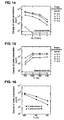
- FIG. 11 is a graph showing a relationship between T1 and density of
oxide precipitates in Experimental Example 1;
- FIG. 12 is a graph showing a relationship between T2 and density of
oxide precipitates in Experimental Example 2;
- FIG. 13 is a graph showing a relationship between Ri and density of
oxide precipitates in Experimental Example 3;
- FIG. 14 is a graph showing a relationship between R2 and density of
oxide precipitates in Experimental Example 4;
- FIG. 15 is a graph showing a relationship between T3 and density of
oxide precipitates in Experimental Example 5;
- FIG. 16 is a graph showing a relationship between T4 and density of
oxide precipitates in Experimental Example 6;
- FIG. 17 is a graph showing a relationship between oxygen
concentration and density of oxide precipitates in Experimental Example 7;
- FIG. 18 is a graph showing a relationship between a keeping time t1
and density of oxide precipitates in Experimental Example 8;
- FIG. 19 is a graph showing a relationship between a temperature
raising rate R and density of oxide precipitates in Experimental Example 9;
- FIG. 20 is a graph showing a relationship between a keeping time t2
and density of oxide precipitates in Experimental Example 10;
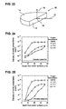
- FIG. 21 is a graph showing a relationship between T5 and density of
oxide precipitates in Experimental Example 11;
- FIG. 22 is a graph showing a relationship between T5 and a DZ
width in Experimental Example 12;
- FIG. 23 is a descriptive view showing a measuring arrangement in
an infrared scattering tomography;
- FIG. 24 is a graph showing a distribution of density of oxide
precipitates in a wafer depth direction in Experimental Example 13;
- FIG. 25 is a graph showing a distribution of density of oxide
precipitates in a wafer depth direction in Experimental Example 14;
- FIG. 26 is a graph showing a relationship between T9 and density of
oxide precipitates in Experimental Example 15;
- FIG. 27 is a graph showing a relationship between oxygen
concentration and density of oxide precipitates in Experimental Example 16;
- FIG. 28 is a graph showing a relationship between a keeping time t5
and density of oxide precipitates in Experimental Example 17;
- FIG. 29 is a graph showing a relationship between a temperature
raising rate R5 and density of oxide precipitates in Experimental Example 18;
- FIG. 30 is a graph showing a relationship between T10 and density of
oxide precipitates in Experimental Example 19;
- FIG. 31 is a graph showing a relationship between a keeping time t6
and density of oxide precipitates in Experimental Example 20;
- FIG. 32 is a graph showing a relationship between T11 and density of
oxide precipitates in Experimental Example 21;
- FIG. 33 is a graph showing a relationship between oxygen
concentration and density of oxide precipitates in Experimental Example 22;
- FIG. 34 is a graph showing a relationship between a keeping time t7
and density of oxide precipitates in Experimental Example 23;
- FIG. 35 is a graph showing a relationship between a temperature
raising rate R6 and density of oxide precipitates in Experimental Example 24;
- FIG. 36 is a graph showing a relationship between a keeping time t8
and density of oxide precipitates in Experimental Example 25; and
- FIG. 37 is a graph showing a relationship between T12 and density of
oxide precipitates in Experimental Example 26.
-
Best Mode for Carrying Out the Invention:
-
Detailed description will be given of embodiments of the present
invention with reference to the accompanying drawings and it is needless to
say that in addition to examples in the figures various modification or
variations may be made without departing from the technical concept of the
present invention.
-
FIG. 1 is a flow chart showing an example of step orders of a first
aspect of a method for manufacturing a silicon wafer of the present invention
and FIG. 2 is a descriptive schematic view showing essential parts of the step
order of FIG. 1. The first aspect of the method for manufacturing a silicon
wafer of the present invention, as shown in FIGs. 1 and 2, comprises the
following indispensable three steps: a temperature raising step A for
generating oxygen precipitation nuclei (step 104); a temperature raising step
B for growing the oxygen precipitation nuclei (step 106); and a constant
temperature keeping step C for growing the oxygen precipitation nuclei into
oxide precipitates of larger sizes (step 108). Note that in FIGs. 1 and 2, there
is shown a preferable case where the temperature raising step A (104), the
temperature raising step B (106) and the constant temperature keeping step
C (108) are continuously performed.
-
As shown in FIG. 1, at first a wafer to be heat-treated is prepared
(step 100). The wafer is loaded into a heat treatment furnace kept at T1°C
(step 102). Here, the T1°C is preferably about 650°C or lower. Then, as well
shown in FIG. 2, a temperature in the furnace is raised from the T1°C to T2°C
at a rate of R1°C/min (a temperature raising step A: step 104). Here, it is
preferably that the T2°C is about 700°C or higher and the R1°C/min is about
1.5°C/min or lower. In the temperature raising step A (step 104), oxygen
precipitation nuclei can be formed at high density. Thereby, even in a wafer
containing almost no oxygen precipitation nuclei at a stage prior to heat
treatment, oxygen precipitation nuclei can be generated at high density. In a
wafer containing oxygen precipitation nuclei in advance, oxygen precipitation
nuclei can be generated at higher density.
-
If there is a desire for changing the density of oxide precipitates to a
level of contamination in a device fabrication process, the density can be
easily changed, for example, by setting the T2°C to about 750°C and the
R1°C/min to about 1°C/min, and changing the T1°C.
-
Then, a temperature in the heat treatment furnace is raised from
the T2°C to T3°C at a rate of R2°C/min (a temperature raising step B: step
106). Here, it is preferable that the T3°C is about 1000°C or higher and the
R2°C/min is the R1°C/min or higher and about 7°C/min or lower. In the
temperature raising step B (step 106), oxygen precipitation nuclei generated
in the previous step can be efficiently grown.
-
Note that, if the temperature raising rates R1°C/min and R2°C/min
in the temperature raising steps A and B are constant, respectively, the
temperature raising steps become preferably uncomplicated, but it is possible
to switch the temperature raising rates in the course of the respective steps.
For example, in the temperature raising step B, temperature raising is
initiated at the temperature raising rate R2°C/min and at a temperature
prior to reaching the T3°C the temperature raising rate may be switched to a
temperature raising rate higher than the R2°C/min, and thereby it is possible
to shorten a process time to some extent.
-
Then, the wafer is kept at the T3°C for t time (a constant
temperature keeping step C: step 108). Here, it is preferable that the T3°C is
about 1000°C or higher and the t time is about 1 hr or longer. In the constant
temperature keeping step C (step 108), minute oxide precipitates generated
in the previous temperature raising steps A and B can be grown into large
oxide precipitates each having an IG capability. Thus, it is an object of the
constant temperature keeping step C to further grow precipitates generated
(grown) in the previous steps. Therefore, as far as the object can be achieved,
this step is not limited literally to keeping a constant temperature but can be
modified to a step accompanied with some temperature changes (raising or
lowering temperatures or the like).
-
Furthermore, by changing the T3°C and the t time in the constant
temperature keeping step C (step 108), sizes of oxide precipitates can be
easily changed. It is considered that the larger the sizes of oxide precipitates
are, the higher the IG capability becomes, but a process time lengthens.
Therefore, in order to attain efficiently oxide precipitates of necessary sizes,
there is important the effect that the sizes are easily changeable.
-
Here, when manufacturing a silicon wafer loaded into a device
fabrication process in which no growth of oxide precipitates is expected, the
T3°C in the constant temperature keeping step C is preferably 1000°C or
higher, but when the present invention is applied in the case where using a
device fabrication process in which growth of oxide precipitates can be
expected, oxide precipitates are not required to be experimentally detected
after heat treatment, the T3°C in the constant temperature keeping step may
be 1000°C or lower, for example, 800°C.
-
After the above heat treatment, for example, a temperature in the
heat treatment furnace is lowered from the T3°C to 800°C at a temperature
lowering rate of 2°C/min (a temperature lowering step D: step 110), and after
that the wafer is unloaded from the heat treatment furnace (step 112).
-
In order to sufficiently achieve the effect of the heat-treating method
of the present invention, oxygen concentration of a silicon wafer is desirably
about 17 ppma or higher. When the oxygen concentration is higher, the
nucleus generating rate and the nucleus growth rate are faster, so a total
process time is shorter.
-
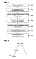
FIG. 3 is a flow chart showing an example of step orders of a second
aspect of a method for manufacturing a silicon wafer of the present invention
and FIG. 4 is a descriptive schematic view showing essential parts of the step
order of FIG. 3.
-
As shown in FIG. 3, at first there is prepared a wafer having
grown-in precipitation nuclei to be heat-treated (step 200). The wafer can be
obtained by processing a silicon single crystal grown by means of an ordinary
CZ method. The wafer is loaded into a heat treatment furnace (step 202).
The heat treatment furnace is maintained at T4°C (500°C to 700°C) and prior
to the next temperature raising step, the loaded wafer is kept at the T4°C for
a prescribed time (t1 time), preferably for 15 min or longer (a keeping step
before temperature raising: step 204). Then, as well shown in FIG. 4, a
furnace temperature is raised from the T4°C to T5°C set in the range of from
1000°C to 1230°C at a temperature raising rate R°C/min of 5°C/min or less (a
temperature raising step: step 206). In the temperature raising step (step
206), grown-in precipitation nuclei of high density can be effectively grown
without annihilation.
-
If there is a desire for changing the density of oxide precipitates to a
level of contamination in a device fabrication process, the density can be
easily changed, for example, by setting the T5°C to about 1100°C and the
temperature raising rate R°C/min to about 3°C/min, and changing the T4°C.
-
Then, the wafer is kept at the T5°C for a prescribed time (t2 time) (a
keeping step after temperature raising: step 208). Here, the keeping time is
preferably about 30 min or longer. In the keeping step after temperature
raising (step 208), minute oxide precipitates in the bulk of a wafer grown in
the previous temperature raising step (step 206) can be grown into oxide
precipitates of desired sizes each on the order of from 30 nm to 40 nm in
diameter, preferably about 50 nm or larger, and at the same time, by
out-diffusing oxygen in the vicinity of a surface of the wafer, oxygen
precipitation nuclei can be annihilated, so that a DZ layer free of oxide
precipitates can be formed.
-
Thus, it is an object of the keeping step after temperature raising
(step 208) at the T5°C to further grow oxide precipitates in the bulk of the
wafer grown in the temperature raising step (step 206) and to out-diffuse
oxygen in the vicinity of a surface of the wafer. Therefore, as far as the object
can be achieved, this step is not limited to keeping a constant temperature
but can be modified to a step accompanied with some temperature changes
(raising or lowering temperatures or the like). Furthermore, by changing the
T5°C and the keeping time t2 in the keeping step after temperature raising
(step 208), sizes of oxide precipitates can be easily changed.
-
Note that the wafer to be heat-treated is irrespective of the presence
or absence of addition of impurities and concentration of impurities. For
example, even a nitrogen-doped wafer can achieve an almost similar effect to
a nitrogen un-doped wafer.
-
After the above heat treatment, for example, a temperature in the
heat treatment furnace is lowered from T5°C to 700°C at a rate of 2°C/min (a
temperature lowering step: step 210), and after that the wafer is unloaded
from the heat treatment furnace (step 212). Note that no specific limitation
is put on the temperature lowering rate and the lowest temperature after the
temperature has been lowered.
-
No specific limitation is put on atmosphere in the above heat
treatment. For example, there can be applied oxygen atmosphere, mixed
atmosphere of oxygen and nitrogen, argon atmosphere, hydrogen atmosphere
and others. In case of non-oxidative atmosphere such as argon and hydrogen,
no oxide film is formed on a surface of a wafer; therefore out-diffusion of
oxygen may be more preferably accelerated as compared with in case of
oxidative atmosphere.
-
In order to sufficiently achieve the effect of the heat-treating method
of the present invention, oxygen concentration in a silicon wafer to be
heat-treated is desirably about 16 ppma or higher. The higher the oxygen
concentration, the higher the density of precipitates; it is possible to impart a
more excellent IG capability to a wafer. Furthermore, the higher the oxygen
concentration, the faster the growth rate of precipitates; a total process time
becomes shorter.
-
FIG. 5 is a flow chart showing an example of step orders of a third
aspect of a method for manufacturing a silicon wafer of the present invention,
and FIG. 6 is a descriptive schematic view showing essential parts of the step
order of FIG. 5. The third aspect of the method for manufacturing a silicon
wafer of the present invention, as shown in FIGs. 5 and 6, comprises the
following three indispensable steps: a temperature raising step Ai for
growing grown-in precipitation nuclei generated in a silicon single crystal
growth step (step 304); a temperature raising step B1 for efficiently raising a
temperature to a higher keeping temperature (step 306); and a constant
temperature keeping step C1 for growing the grown-in precipitation nuclei to
oxide precipitates of sizes each equal to or larger than one having a gettering
capacity and for out-diffusing oxygen in the vicinity of a surface of the silicon
wafer (step 308). Note that in FIGs. 5 and 6, there is shown a preferable case
where the temperature raising step A1 (step 304), the temperature raising
step B1 (step 306) and the constant temperature keeping step C1 (step 308)
are continuously performed.
-
As shown in FIG. 5, at first there is prepared a wafer having
grown-in precipitation nuclei to be heat-treated (step 300). This wafer can be
obtained by processing a silicon single crystal grown by means of an ordinary
CZ method. The wafer is loaded into a heat treatment furnace maintained at
T6°C (step 302). Here, the T6°C is preferably 700°C or lower. Then, as well
shown in FIG. 6, a temperature in the heat treatment furnace is raised from
the T6°C to T7°C at a rate of R3°C/min (a temperature raising step A1: step
304). Here, it is preferable that the T7°C is 800°C to 1000°C and the
R3°C/min is 3°C/min or less. Furthermore, prior to temperature raising from
the T6°C to the T7°C in the temperature raising step A1 (step 304), a keeping
time t3 at the T6°C may be 0 min without hindrance, but more preferably 30
min or longer. In the temperature raising step A1 (step 304), grown-in
precipitation nuclei of high density can be efficiently grown without
annihilation.
-
Then, a temperature in the heat treatment furnace is raised from
the T7°C to T8°C at a rate of R4°C/min (a temperature raising step B1: step
306). Here, it is preferable that the T8°C is 1050°C to 1230°C and the
R4°C/min is 5°C/min or more. In the temperature raising step B1 (step 306),
by raising a temperature to a higher keeping temperature for a short time,
there is avoided growth of more precipitates than necessary so that
precipitates in the vicinity of a surface of the wafer can be easily annihilated.
-
Then, the wafer is kept at the T8°C for t4 time (a constant
temperature keeping step C1: step 308). Here, it is preferable that the T8°C is
1050°C to 1230°C and the t4 time is about 30 min or longer. In the constant
temperature keeping step C1 (step 308), minute oxide precipitates in the bulk
of the wafer grown in the previous temperature raising steps (steps 304 and
306) are grown into oxide precipitates of desired sizes each of about 40 nm or
larger in diameter and preferably about 50 nm or larger, and at the same
time, by out-diffusing oxygen in the vicinity of a surface of the wafer, oxide
precipitates are annihilated, so that a DZ layer free of oxide precipitates can
be formed.
-
In this case, as compared with a DZ layer formed in the second
aspect of the present invention, oxide precipitates in the vicinity of the
surface region of a wafer can be annihilated more perfectly; therefore, an
extremely high quality DZ layer can be efficiently obtained.
-
Thus, it is an object of the constant temperature keeping step C1 at
the T8°C (step 308) to further grow oxide precipitates in the bulk of the wafer
grown in the temperature raising steps (steps 304 and 306) and to out-diffuse
oxygen in the vicinity of a surface of the wafer. Therefore, as far as the
purposes can be achieved, the constant temperature keeping step C1 is not
limited to keeping a wafer at a constant temperature but the step can be
modified to a step accompanied with some temperature changes (raising or
lowering temperatures or the like). Furthermore, by changing the T8°C and
the keeping time t4 in the constant keeping step C1 (step 308), sizes of oxide
precipitates and a DZ width can be easily changed.
-
Note that the wafer to be heat-treated is irrespective of the presence
or absence of addition of impurities and concentration of impurities. For
example, even a nitrogen-doped wafer can achieve an almost similar effect to
a nitrogen un-doped wafer.
-
After the above heat treatment, for example, a temperature in the
heat treatment furnace is lowered from the T8°C to 700°C at 3°C/min (a
temperature lowering step D1: step 310), and after that the wafer is unloaded
from the heat treatment furnace (step 312). Note that no specific limitation
is put on the temperature lowering rate and the lowest temperature after the
temperature has been lowered.
-
No specific limitation is put on atmosphere in the above heat
treatment. For example, there can be applied oxygen atmosphere, mixed
atmosphere of oxygen and nitrogen, argon atmosphere, hydrogen atmosphere
and others. In case of non-oxidative atmosphere such as argon and hydrogen,
no oxide film is formed on a surface of a wafer; therefore out-diffusion of
oxygen may be more preferably accelerated as compared with in case of
oxidative atmosphere.
-
In order to sufficiently achieve the effect of the third aspect of the
method for manufacturing a silicon wafer of the present invention, oxygen
concentration in a silicon wafer to be heat-treated is desirably about 14 ppma
to 17 ppma. When the oxygen concentration is higher, the density of
precipitates is raised; it is possible to impart a more excellent IG capability to
a wafer, but if the oxygen concentration is excessively high, precipitates in
the vicinity of a surface of the wafer are hard to be annihilated. On the other
hand, when the oxygen concentration is lower, the density of grown-in
precipitates generated in a silicon single crystal growth step becomes lower;
the density of precipitates is reduced. However, even when oxygen
concentration is low, for example, by lowering the temperature raising
initiation temperature T6°C or slowing the R3°C/min in the temperature
raising step A1, the effect of the third aspect of the method for manufacturing
a silicon wafer of the present invention can be achieved.
-
FIG. 7 is a flow chart showing an example of step orders of a first
aspect of a method for manufacturing a silicon epitaxial wafer of the present
invention and FIG. 8 is a descriptive schematic view showing essential parts
of the step order of FIG. 7.
-
As shown in FIG. 7, at first there is prepared a wafer having
grown-in precipitation nuclei to be heat-treated (step 400). This wafer can be
obtained by processing a silicon single crystal grown by means of an ordinary
CZ method. The wafer is loaded into a heat treatment furnace (step 402).
The heat treatment furnace is maintained at T9°C (500°C to 700°C) and the
loaded wafer is kept at the T9°C for a prescribed time (t5 time), preferably 15
min or longer, prior to performing the next temperature raising step (a
keeping step before temperature raising: step 404). Then, as well shown in
FIG. 8, a temperature in the heat treatment furnace is raised from the T9°C
to T10°C set in the range of from 800°C to 900°C at a temperature raising rate
R5°C/min of 5°C/min or less (a temperature raising step: step 406). In the
temperature raising step (step 406), grown-in precipitation nuclei of high
density can be efficiently grown without annihilation.
-
If there is a desire for changing the density of oxide precipitates to a
level of contamination in a device fabrication process, the density can be
easily changed, for example, by setting the T10°C to about 800°C and the
temperature raising rate R5°C/min to about 3°C/min, and changing the T9°C.
-
Then, the wafer is kept at the T10°C for a prescribed time (t6 time) (a
keeping step after temperature raising: step 408). Here, the keeping time is
preferably about 30 min or longer. In the keeping step after temperature
raising (step 408), minute oxide precipitates grown in the previous
temperature raising step (step 406) can be grown into oxide precipitates of
desired sizes each of 30 nm to 40 nm, preferably 50 nm or larger. Thus, it is
an object of the keeping step after temperature raising (step 408) at the T10°C
to further grow oxide precipitates grown in the temperature raising step
(step 406). Therefore, as far as the object can be achieved, this step is not
limited to keeping a constant temperature but can be modified to a step
accompanied with some temperature changes (raising or lowering
temperatures or the like).
-
Furthermore, by changing the T10°C and the keeping time t6 in the
keeping step after temperature raising (step 408), sizes of oxide precipitates
can be easily changed.
-
Note that the wafer to be heat-treated is irrespective of the presence
or absence of addition of impurities and concentration of impurities. For
example, even a nitrogen-doped wafer can achieve an almost similar effect to
a nitrogen un-doped wafer.
-
After the above heat treatment, for example, a temperature in the
heat treatment furnace is lowered from the T10°C to 700°C at a rate of
2°C/min (a temperature lowering step: step 410), and after that the wafer is
unloaded from the heat treatment furnace (step 412). Note that no specific
limitation is put on the temperature lowering rate and the lowest
temperature after the temperature has been lowered.
-
Then, if required, there are performed such processes as wafer
cleaning and oxide film removing, and after that epitaxial growth is carried
out (step 414). In this case, while sizes of oxide precipitates immediately
after the epi step are not so large as to have an enough IG capability, the
oxide precipitates grow to sizes each having an IG capability by heat
treatment in a device fabrication process into which the wafer is loaded after
the epi step; an excellent IG capability is imparted to the wafer.
-
The above heat treatment according to the present invention may be
applied to a wafer to be heat-treated before or after mirror polishing (may be
referred to as mechanical chemical polishing). In the case where the heat
treatment is performed before the mirror polishing, the mirror polishing is
applied after the heat treatment and then epitaxial growth follows.
-
In order to sufficiently achieve the effect of the heat-treating method
of the present invention, oxygen concentration of a silicon wafer to be
heat-treated is desirably about 16 ppma or higher. When the oxygen
concentration is higher, the density of precipitates is raised; it is possible to
impart a more excellent IG capability to a wafer. Furthermore, the higher
the oxygen concentration is, the faster the growth rate of the precipitates
becomes, so a total process time is shortened.
-
FIG. 9 is a flow chart showing an example of step orders of a second
aspect of a method for manufacturing a silicon epitaxial wafer of the present
invention and FIG. 10 is a descriptive schematic view showing essential parts
of the step order of FIG. 9.
-
As shown in FIG. 9, at first there is prepared a wafer having
grown-in precipitation nuclei to be heat-treated (step 500). This wafer can be
obtained by processing a silicon single crystal grown by means of an ordinary
CZ method. The wafer is loaded into a heat treatment furnace (step 502).
The heat treatment furnace is maintained at T11°C (500°C to 700°C) and the
loaded wafer is kept at the T11°C for a prescribed time (t7 time), preferably 15
min or longer, prior to performing the next temperature raising step (a
keeping step before temperature raising: step 504). Then, as well shown in
FIG. 10, a temperature in the heat treatment furnace is raised from the T11°C
to T12°C set in the range of from 1000°C to 1100°C at a temperature raising
rate R6°C/min of 5°C/min or less (a temperature raising step: step 506). In
the temperature raising step (step 506), grown-in precipitation nuclei of high
density can be efficiently grown without annihilation.
-
If there is a desire for changing the density of oxide precipitates to a
level of contamination in a device fabrication process, the density can be
easily changed, for example, by setting the T12°C to about 1000°C and the
temperature raising rate R6°C/min to about 3°C/min, and changing the T11°C.
-
Then, the wafer is kept at the T12°C for a prescribed time (ts time) (a
keeping step after temperature raising: step 508). Here, the keeping time is
preferably about 30 min or longer. In the keeping step after temperature
raising (step 508), minute oxide precipitates grown in the previous
temperature raising step (step 506) can be grown into oxide precipitates of
desired sizes each of the order of from 30 nm to 40 nm in diameter, preferably
of 50 nm or larger. Thus, it is an object of the keeping step after temperature
raising (step 508) at the T12°C to further grow oxide precipitates grown in the
temperature raising step (step 506). Therefore, as far as the object can be
achieved, this step is not limited to keeping a constant temperature but can
be modified to a step accompanied with some temperature changes (raising or
lowering temperatures or the like).
-
Furthermore, by changing the T12°C and the keeping time t8 in the
keeping step after temperature raising (step 508), sizes of oxide precipitates
can be easily changed.
-
Note that the wafer to be heat-treated is irrespective of the presence
or absence of addition of impurities and concentration of impurities. For
example, even a nitrogen-doped wafer can achieve an almost similar effect to
a nitrogen un-doped wafer.
-
After the above heat treatment, for example, a temperature in the
heat treatment furnace is lowered from the T12°C to 700°C at a rate of
2°C/min (a temperature lowering step: step 510), and after that the wafer is
unloaded from the heat treatment furnace (step 512). Note that no specific
limitation is put on the temperature lowering rate and the lowest
temperature after the temperature has been lowered.
-
Then, if required, there are performed such processes as wafer
cleaning and oxide film removing, and after that epitaxial growth is carried
out (step 514). In this case, no re-dissolution of oxide precipitates occurs
during the epitaxial growth step; there can be obtained a silicon epitaxial
wafer in which oxide precipitates of sizes each having an IG capability are
generated before being loaded into a device fabrication process.
-
The heat treatment may be applied to a wafer to be heat-treated
before or after mirror polishing (may be referred to as mechanical chemical
polishing). In the case where the heat treatment is performed before the
mirror polishing, the mirror polishing is applied after the heat treatment and
then epitaxial growth follows.
-
In order to sufficiently achieve the effect of the heat-treating method
of the present invention, oxygen concentration of a silicon wafer to be
heat-treated is desirably about 16 ppma or higher. When the oxygen
concentration is higher, the density of precipitates is raised; it is possible to
impart a more excellent IG capability to a wafer. Furthermore, the higher
the oxygen concentration is, the faster the growth rate of the precipitates
becomes, so a total process time is shortened.
Examples
-
While description will be given of the present invention showing
Experimental Examples below, the present invention is not limited to the
Experimental Examples.
(Experimental Examples 1 to 5)
-
There were prepared boron-doped silicon wafers each having a
diameter of 8 inches, a plane orientation of < 100 > and resistivity of about 10
Ω·cm grown by means of a CZ method. Oxygen concentrations of the wafers
were 16.0, 17.0, 18.5 and 19.5 ppma, respectively (JEIDA scale). The wafers
were all subjected to heat treatment at 1050°C for 1 hr. With the aid of the
heat treatment, almost all oxygen precipitation nuclei formed in a crystal
thermal history are annihilated. By this treatment, for example, there can be
simulated states of an epi wafer containing almost no oxygen precipitation
nuclei and a wafer heat-treated at a temperature of 1000°C or higher in
advance. Note that JEIDA is an abbreviation for Japan Electronic Industry
Development Association (now renamed JEITA: Japan Electronics and
Information Technology Industries Association).
-
Next, heat treatment shown in FIGs. 1 and 2 was applied to the
wafers. That is, a temperature was raised from T1°C to T2°C at a rate of
R1°C/min, from the T2°C to T3°C at a rate of R2°C/min and kept at the T3°C for
t time. After the keeping, a temperature in a heat treatment furnace was
lowered to 800°C at a rate of 2°C/min and then the wafer was unloaded from
the heat treatment furnace.
-
The density of oxide precipitates in the bulk of the heat-treated
wafer was measured with an infrared scattering tomography method
(hereinafter may be referred to LST), which is one of infrared scattering
methods. Note that, while Experimental Examples 1 to 5 include ones
carried out in the same heat treatment condition, they are performed as
independent experiments using separate wafers; there are some differences
among measured values of the density of oxide precipitates, the differences
being inessential.
-
FIG. 11 shows the density of oxide precipitates at 550°C, 600°C and
650°C of the T1°C (Experimental Example 1). In this case, the other
conditions were as follows: T2 = 750°C, R1 = 1°C/min, T3 = 1050°C, R2 =
3°C/min and t = 2 hrs. The lower the T1°C is, the higher the density of oxide
precipitates becomes. This is because the lower the temperature is, the faster
the precipitation nucleus forming rate becomes and the longer the
temperature raising time becomes, thereby a time for generating
precipitation nuclei being longer. Furthermore, the higher the oxygen
concentration is, the higher the density of oxide precipitates becomes. This is
because the higher the oxygen concentration is, the faster the precipitation
nucleus forming rate becomes. In order to obtain an IG capability, the
density of oxide precipitates is desirably on the order of 108 /cm3 or higher.
This indicates that the T1°C is preferably about 650°C or lower. Further, it is
found that the oxygen concentration is preferably about 17 ppma or higher in
order to attain oxide precipitates of high density. Furthermore, as shown in
FIG. 11, by changing the T1°C, the density of oxide precipitates can be easily
changed. This is effective where there is a desire for obtaining requested
density of oxide precipitates to a level of contamination in a device fabrication
process.
-
FIG. 12 shows the density of oxide precipitates at 700°C, 750°C,
800°C and 850°C of the T2°C (Experimental Example 2). In this case, the
other conditions were as follows: T1 = 600°C, R1= 1°C/min, T3 = 1050°C, R2 =
3°C/min and t = 2 hrs. When the oxygen concentration is about 17 ppma or
higher, the density of oxide precipitates shows almost no change at the T2°C
of 750°C or higher. This is because since formation of precipitation nuclei is
hard to progress in a temperature raising step at a temperature of 750°C or
higher, the density of oxygen precipitation nucleus is almost unchanged. The
fact that the density of oxide precipitates is low at 700°C is because the
density of oxygen precipitation nuclei formed is low due to a short time of the
temperature raising step A. This indicates that the density of oxide
precipitates can be higher by setting the T2°C to about 700°C or higher,
preferably about 750°C or higher.
-
FIG. 13 shows the density of oxide precipitates 1°C/min, 1.5°C/min,
2°C/min, 2.5°C/min and 4°C/min of the R1°C/min (Experimental Example 3).
In this case, the other conditions were as follows: T1 = 600°C, T2 = 750°C, T3 =
1050°C, R2 = 3°C/min and t = 2 hrs. The lower the R1°C/min is, the higher the
density of oxide precipitates becomes. This is because the lower the rate is,
the longer the time for generating precipitation nuclei becomes. From FIG.
13, it is found that the R1°C/min is preferably about 1.5°C/min or less in order
to attain oxide precipitates of high density.
-
FIG. 14 shows the density of oxide precipitates at 1°C/min, 3°C/min,
5°C/min, and 7°C/min of the R2°C/min (Experimental Example 4). In this
case, the other conditions were as follows: T1 = 600°C, T2 = 750°C, R1 =
1°C/min, T3 = 1050°C, and t = 2 hrs. The slower the R2°C/min is, the higher
the density of oxide precipitates becomes. This is because at a slower rate,
more of oxygen precipitation nuclei formed in the previous stage can grow
into oxide precipitates without annihilation. To the contrary, when the rate
is faster, the proportion of oxygen precipitation nuclei to be annihilated
becomes higher; the density of oxide precipitates is reduced. From FIG. 14, it
is found that the R2°C/min is about 7°C/min or less, preferably about 5°C/min
or less in order to attain oxygen precipitates of high density.
-
FIG. 15 shows the density of oxide precipitates at 950°C, 1000°C,
1050°C and 1100°C of the T3°C (Experimental Example 5). In this case, the
other conditions were as follows: T1 = 600°C, T2 = 750°C, R1= 1°C/min, R2 =
3°C/min and t = 1 hr. At the T3 of 1000°C or higher, the density of oxide
precipitates is almost unchanged. This is because at 1000°C or higher, oxide
precipitates have been sufficiently grown to detectable sizes. The fact that
the density of oxide precipitates is low at 950°C is because at the keeping
time of 1 hr, the proportion of oxide precipitates not to grow up to detectable
sizes is high. In this case, if the keeping time is longer, the density of
detectable oxide precipitates becomes to the same level in case of 1000°C or
higher, but a longer process time is required. This indicates that the T3°C is
preferably about 1000°C or higher.
-
As can be seen from the above description, by setting the Ti to about
650°C or lower, the T2°C to about 700°C or higher, the R1°C /min to about
1.5°C/min or less, the R2°C /min to about 7°C/min or less, the T3°C to about
1000°C or higher and the t time to about 1 hr or longer, respectively, oxide
precipitates of large sizes can be efficiently generated even in a wafer
containing almost no oxygen precipitation nuclei. That is, there can be stably
provided a wafer having an excellent IG capability at a stage prior to a device
fabrication process. Further, even in wafers having fluctuations in density of
oxygen precipitation nuclei due to different crystal thermal histories, by
performing the heat treatment in the method for manufacturing a silicon
wafer of the present invention after the heat treatment has been carried out
for annihilating the oxygen precipitation nuclei thereof as in these
Experimental Examples, fluctuations in the IG capabilities thereof can be
reduced.
(Experimental Examples 6 to 10)
-
There were prepared mirror-polished silicon wafers each having a
diameter of 8 inches, a plane orientation of < 100 > and resistivity of about 10
Ω·cm, which were manufactured from different two portions (these portions
belong to positions grown in the former half and the latter half of the crystal
growth step and hereinafter may be referred to as a crystal position A and a
crystal position B, respectively) of a boron-doped silicon single crystal grown
by means of a CZ method. Oxygen concentrations of the wafers are 16 ppma
to 20 ppma (JEIDA scale).
-
Next, the wafers were subjected to heat treatment in atmosphere of
a mixture of oxygen and nitrogen according to a procedure shown in FIGs. 3
and 4. That is, the wafer was kept at T4°C for t1 time, thereafter the
temperature was raised from the T4°C to T5°C at a rate of R°C/min and kept
at the T5°C for t2 time. After the keeping, the temperature in a heat
treatment furnace was lowered to 700°C at a rate of 2°C/min and then the
wafers were unloaded from the heat treatment furnace. The density of oxide
precipitates in the bulk of the wafer was measured with the LST without any
heat treatment. According to the LST, there are detectable oxide precipitates
having sizes of about 40 nm or larger in diameter.
-
FIG. 16 shows the density of precipitates at 600°C, 700°C, and 800°C
of the T4°C (Experimental Example 6). In this case, the other conditions were
as follows: t1 = 30 min, R = 3°C/min, T5°C = 1050°C and t2 = 2hrs. Oxygen
concentrations are 16 ppma to 18 ppma. The lower the T4°C is, the higher the
density of precipitates becomes. This is because there is increased the
density of grown-in precipitation nuclei which grow at a lower temperature
without annihilation. In order to obtain an excellent IG capability, the
density of precipitate is desirably on the order of 109 /cm3 or higher. This
indicates that the T4°C is about 700°C or lower. Moreover, as shown in FIG.
16, by changing the T4°C, the density of precipitates can be easily changed.
This is effective where there is a desire for obtaining requested density of
precipitates to a level of contamination in a device fabrication process.
-
FIG. 17 shows the oxygen concentration dependence of density of
precipitates at T4 = 700°C, t1 = 30 min, R = 3°C/min, T5 = 1050°C and t2 = 2
hrs (Experimental Example 7). This result indicates that in either crystal
position there is a trend that as the oxygen concentration increases, the
density of oxide precipitates increases. It is also found that when an oxygen
concentration is about 16 ppma or higher, the high density of precipitates of
the order of 109 /cm3 or higher can be surely achieved. This is because the
higher the oxygen concentration is, the higher the density of grown-in
precipitation nuclei becomes and the larger the sizes of oxide precipitates
becomes, thereby the detectable proportion thereof being increased.
-
FIG. 18 shows the density of precipitates at 0 min, 5 min, 15 min, 30
min and 45 min of the t1 time (Experimental Example 8). In this case, the
other conditions were as follows: T4 = 700°C, R = 3°C/min, T5 = 1050°C and t2
= 2 hrs. Oxygen concentrations are 18 ppma to 20 ppma. When the t1 time is
about 15 min or longer, the density of precipitates increases with time. This
is because as the t1 time is longer, the proportion of grown-in precipitation
nuclei to be grown without annihilation becomes higher and new
precipitation nuclei are generated for the keeping of the ti time. This result
indicates that even in the case where the t1 time is shorter than 15 min, the
high density of precipitates can be achieved, but in the case where the ti time
is 15 min or longer, the density of precipitates is further increased; it is found
that the latter case is more preferable.
-
FIG. 19 shows the density of precipitates at 1°C/min, 3°C/min and
5°C/min of the R°C/min (Experimental Example 9). In this case, the other
conditions were as follows: T4 = 700°C, t1 = 30 min, T5 = 1050°C and t2 = 2 hrs.
Oxygen concentrations are 18 ppma to 20 ppma. The slower the R°C/min is,
the higher the density of precipitates becomes. The reason why when the
R°C/min is faster, the density of precipitates becomes lower is that there
becomes higher the proportion of precipitation nuclei which are annihilated
without growth in the temperature raising step. This result indicates that in
order to achieve the high density of precipitates of the order of 109 /cm3 or
higher, the R°C/min is preferably about 5°C/min or less, more preferably
about 3°C/min or less.
-
FIG. 20 shows the density of oxide precipitates at 30 min, 60 min
and 120 min of the t2 time (Experimental Example 10). In this case, the other
conditions were as follows: T4 = 700°C, t5 = 30 min, R = 3°C/min, T5 = 1100°C.
Oxygen concentrations are 18 ppma to 20 ppma. The density of precipitates
is high almost independently of the t2 time. This result indicates that when
the t2 time is about 30 min or longer, the high density of precipitates is surely
achieved.
(Experimental Example 11)
-
Mirror-polished wafers similar to the wafers used in Experimental
Examples 6 to 10 were prepared. Then, according to a heat treatment
procedure shown in FIGs. 3 and 4, the following conditions were applied: T4 =
700°C, t1 = 30 min, R = 3°C/min and t2 = 2 hrs, and there were performed 4
levels of heat treatment where T5°C was changed to 950°C, 1000°C, 1050°C
and 1100°C, respectively. After the keeping at the T5°C, the temperature in a
heat treatment furnace was lowered to 700°C at 2°C/min and then the wafers
were unloaded from the heat treatment furnace. The density of oxide
precipitates in the bulk of the wafer was measured with the LST without any
heat treatment.
-
FIG. 21 shows a relationship between density of precipitates and
T5°C in the Experimental Example. Oxygen concentrations are 18 ppma to
20 ppma. When the T5°C is 1000°C or higher, the density of precipitates
becomes high. The reason why the density of oxide precipitates decreases at
950°C is that a growth rate of the precipitates is slower than at 1000°C or
higher and hence sizes of precipitates are too small to be detectable by the
LST. This result indicates that in order to generate precipitates of large sizes
at high density at a stage prior to a device fabrication process, the T5°C is
preferably about 1000°C or higher.
(Experimental Example 12)
-
Mirror-polished wafers similar to the wafers used in Experimental
Examples 6 to 11 were prepared. Then, according to a heat treatment
procedure shown in FIGs. 3 and 4, the following conditions were applied: T4 =
700°C, t1 = 30 min, R = 3°C/min and t2 = 2 hrs, and there were performed 3
levels of heat treatment where the T5°C was changed to 1000°C, 1050°C and
1100°C, respectively. After the keeping at the T5°C, the temperature in a
heat treatment furnace was lowered to 700°C at 2°C/min and then the wafers
were unloaded from the heat treatment furnace.
-
The heat-treated wafers were cleaved and then subjected to
chemical preferential etching. Thereafter, by observing a cleaved surface
thereof through an optical microscope, there was measured a depth from a
wafer surface of the region where no etch pits due to oxide precipitates were
observed (hereinafter may be referred to as a DZ width).
-
A relationship between a DZ width obtained in the above
measurement and the T5°C is shown in FIG. 22. Oxygen concentrations are
18 ppma to 20 ppma. The higher the T5°C is, the wider the DZ width becomes.
This is because the higher the temperature is, the faster the diffusion rate of
oxygen becomes; oxygen in the vicinity of a wafer surface is out-diffused, so
that oxygen precipitation nuclei in the vicinity of the wafer surface are
annihilated.
-
As described above, by setting the T4°C to about 700°C or lower, the
R°C/min to about 5°C/min or less, the T5°C to about 1000°C or higher and the
t2 time to about 30 min or longer, respectively, a silicon wafer having a
defect-free layer (DZ layer) in the vicinity of a surface thereof and oxide
precipitates each having a high gettering capability in the bulk thereof can be
attained with the aid of an extremely efficient and simple heat treatment.
(Experimental Example 13)
-
There were prepared boron-doped silicon wafers each having a
diameter of 8 inches, a plane orientation < 100 > and resistivity of about 10
Ω · cm grown by means of a CZ method. Each of these wafers is one having a
few defects with few COPs and voids which is manufactured from a silicon
single crystal pulled in a condition that suppresses generation of void defects
in growth thereof. Oxygen concentrations of the wafers were 14.5, 15.4 and
17.0 ppma, respectively (JEIDA scale).
-
Next, the wafers were subjected to heat treatment in atmosphere of
a mixture of oxygen and nitrogen according to a procedure shown in FIGs. 3
and 4. That is, the wafer was kept at 700°C for 1 hr, then the temperature
was raised up to 1150°C at a rate of 3°C/min and kept at 1150°C for 4 hrs.
After the keeping, the temperature in a heat treatment furnace was lowered
to 700°C at a rate of 3°C/min and then the wafers were unloaded from the
heat treatment furnace. There was measured a depthwise distribution of
density of oxide precipitates from a position in the vicinity of a surface of each
wafer to another position in the bulk thereof with the LST without any heat
treatment.
-
There is shown a measuring arrangement with the LST in
measurement of a depthwise distribution of density of oxide precipitates in
FIG. 23. An infrared beam 12 is incident upon a cleaved surface 10 of a
cleaved wafer W and there is detected scattering light 16 from precipitates
coming out of a wafer surface 14. In this measurement, by changing a
distance from the surface of the incident point 18 (a depth from the surface)
at the intervals of 5 µm in the range of 5 µm to 35 µm, the depthwise
distribution of density of precipitates was measured. The depth resolution in
this case is on the order of ± 5 µm. Accordingly, for example, the density of
precipitates at a point of 10 µm in depth actually shows an average value
thereof in a region of the order of 5 µm to 15 µm in depth.
-
FIG. 24 shows results of measurement of the depthwise distribution
of density of precipitates. In this case, the density of precipitates at the
positions of 5 µm in depth in the wafers having any oxygen concentrations
was on the order of 106 /cm3 to 107 /cm3. These results indicate that a region
on the order of 0 µm to 10 µm deep is effective as a DZ layer, but precipitates
of low density still remain therein.
-
Further, there was separately prepared a wafer similar to the above
wafers except for the oxygen concentration of 18 ppma. The wafer was
subjected to heat treatment where the wafer was kept at 700°C for 1hr, then
the temperature was raised to 1200°C at a rate of 3°C/min and kept at
1200°C for 1 hr.
-
Furthermore, the density of oxide precipitates of the heat-treated
wafer was observed, and the results indicate that in a region of about 10 µm
deep from a wafer surface, there was formed a DZ layer where precipitates
remain at low density of the order of 107 /cm3 or lower, and in the bulk portion
deeper than the layer, the density of oxide precipitates of about 5 × 10⁹ /cm3
were obtained.
(Experimental Example 14)
-
There were prepared wafers similar to the wafers used in
Experimental Example 13. Then, the wafers were subjected to heat
treatment in atmosphere of a mixture of oxygen and nitrogen according to a
procedure shown in FIGs. 5 and 6. That is, the wafer was kept at 700°C for 1
hr, then the temperature was raised to 900°C at a rate of 3°C/min, further
raised from 900°C to 1150°C at a rate of 5°C/min and kept at 1150°C for 4 hrs.
After the keeping, the temperature in a heat treatment furnace was lowered
to 700°C at a rate of 3°C/min and the wafers were unloaded from the heat
treatment furnace. That is, unlike in Experimental Example 13 (the second
embodiment of the present invention), there was carried out such heat
treatment as the temperature raising rate was faster from the middle of the
temperature raising step (which corresponds to the third embodiment of the
present invention). There was measured a depthwise distribution of density
of precipitates of each wafer without any heat treatment according to the
method similar to Experimental Example 13 with the LST.
-
FIG. 25 shows results of measurement of a depthwise distribution of
a density of precipitates. In a wafer having any oxygen concentrations, the
density of precipitates at the position 5 µm deep was the detection lower limit
(about 1 × 10⁶ /cm3) or less. This results indicate that there exists no
detectable precipitates in the region of the order of 0 µm to 10 µm deep. That
is, it is found that there is formed a DZ layer of an extremely high quality.
Further, it is found that when the oxygen concentration is low, the DZ layer
is wider. This is because the lower the oxygen concentration prior to the heat
treatment, the lower the oxygen concentration in a surface region in the
vicinity of a surface of the heat-treated wafer, thereby precipitates in the
vicinity of the surface thereof being easily annihilated. On the other hand, it
is found that the density of precipitates in the interior of the wafer is 1 × 10⁹
/cm3 or higher; an excellent IG capability can be expected.
-
Furthermore, there was separately prepared a wafer similar to the
wafers used in Experimental Example 13 except for the oxygen concentration
of 16 ppma. The wafer was subjected to heat treatment where the wafer was
kept at 700°C for 1 hr, then the temperature was raised to 900°C at a rate of
3°C/min, further raised from 900°C to 1200°C at a rate of 5°C/min and kept at
1200°C for 1 hr.
-
Then, the density of oxide precipitates of the heat-treated wafer was
observed, and the results indicate that in a region of about 10 µm deep from a
wafer surface, there was formed a DZ layer having density of oxide
precipitates of 1 × 10⁶ /cm3 or lower, and in the bulk portion deeper than the
layer, the density of oxide precipitates of about 3 × 10⁹/cm3 were obtained.
-
As described above, according to the third aspect of the method for
manufacturing a silicon wafer of the present invention, there can be formed a
high quality DZ-IG structure which combines a DZ layer containing few
precipitates and an IG layer having an excellent IG capability.
(Experimental Examples 15 to 20)
-
There were prepared silicon wafers each having a diameter of 8
inches, a plane orientation of < 100 > and resistivity of about 10 Ω·cm, which
were sliced from different two portions (these portions belong to positions
grown in the former half and the latter half of the crystal growth step and
hereinafter may be referred to as a crystal position A and crystal position B,
respectively) of a boron-doped silicon single crystal grown by means of a CZ
method. The wafers prepared here were chemical etched wafers that are not
subjected to mirror polishing. Oxygen concentrations of the wafers are 16
ppma to 20 ppma (JEIDA scale).
-
Then, the wafers were subjected to heat treatment according to the
procedure shown in FIGs. 7 and 8. That is, the wafer was kept at T9°C for t5
time, thereafter the temperature was raised from the T9°C to T10°C at a rate
of R5°C/min and kept at the T10°C for t6 time. After the keeping, the
temperature in a heat treatment furnace was lowered to 700°C at a rate of
2°C/min and then the wafers were unloaded from the heat treatment furnace.
-
After the heat-treated wafers were mirror-polished, a silicon single
crystal layer about 3 µm thick was deposited on each of the mirror-polished
wafers by epitaxial growth at about 1100°C to thereby obtain epi wafers.
-
After the epi wafers were subjected to heat treatment at 1000°C for 2
hrs that simulates a device fabrication process with a low temperature and a
short time, the density of oxide precipitates in the bulk of the wafer below the
epitaxial layer of each epi wafer was measured with the LST. With the LST,
there are detectable oxide precipitates having sizes of about 40 nm or larger
in diameter.
-
FIG. 26 shows the density of precipitate at values 600°C, 700°C, and
800°C of the T9°C (Experimental Example 15). In this case, the other
conditions were as follows: t5 = 30 min, R5 = 3°C/min, T10°C = 850°C and t6 =
1hr. Oxygen concentrations are in the range of from 16 ppma to 18 ppma.
The lower the T9°C is, the higher the density of precipitates becomes. This is
because there is increased the density of grown-in precipitation nuclei which
grow at a lower temperature without annihilation. In order to obtain an
excellent IG capability, the density of precipitates is desirably on the order of
109/cm3 or higher. This indicates that the T9°C is preferably about 700°C or
lower. Moreover, as shown in FIG. 26, by changing the T9°C, the density of
precipitates can be easily changed. This is effective where there is a desire
for obtaining requested density of precipitates to a level of contamination in a
device fabrication process.
-
FIG. 27 shows the oxygen concentration dependence of density of
precipitates at T9 = 700°C, t5 = 30 min, R5 = 3°C/min, T10 = 850°C and t6 = 1 hr
(Experimental Example 16). This result indicates that in either crystal
positions there is a trend that as the oxygen concentration increases, the
density of oxide precipitates increases. It is also found that when the oxygen
concentration is about 16 ppma or higher, the high density of precipitates of
the order of 109 /cm3 or higher can be surely achieved. This is because the
higher the oxygen concentration is, the higher the density of grown-in
precipitation nuclei becomes and the larger the sizes of oxide precipitates
becomes, thereby a proportion of the detectable precipitates being increased
after the heat treatment at 1000°C for 2 hrs.
-
FIG. 28 shows the density of precipitates at 0 min, 5 min, 15 min, 30
min and 45 min of the t5 time (Experimental Example 17). In this case, the
other conditions were as follows: T9 = 700°C, R5 = 3°C/min, T10°C = 850°C and
t6 = 1 hr. Oxygen concentrations are 16 ppma to 18 ppma. When the t5 time
is 15 min or longer, there is a trend that the density of precipitates increases
with time. This is because as the t5 time is longer, the proportion of grown-in
precipitation nuclei to be grown without annihilation becomes higher and
new precipitation nuclei are generated during the keeping of the t5 time.
This result indicates that even in the case where the t5 time is shorter than
15 min, the high density of precipitates can be achieved, but in the case
where the t5 time is 15 min or longer, the density of precipitates is further
increased; it is found that the latter case is more preferable.
-
FIG. 29 shows the density of oxide precipitates at 1°C/min, 3°C/min
and 5°C/min of the R5°C/min (Experimental Example 18). In this case, the
other conditions were as follows: T9 = 700°C, t5 = 30 min, T10 = 850°C, t6 = 1 hr.
Oxygen concentrations are 16 ppma to 18 ppma. The lower the R5°C/min is,
the higher the density of precipitates becomes. The reason why when the
R5°C/min is faster, the density of precipitates becomes lower is that there
becomes higher the proportion of precipitation nuclei which are annihilated
without growth in the temperature raising step. This result indicates that
the high density of precipitates of the order of 109 /cm3 or higher can be surely
attained at the R5°C/min of about 5°C/min or less.
-
FIG. 30 shows the density of oxide precipitates at 750°C, 800°C,
850°C and 900°C of the T10 (Experimental Example 19). In this case, the
other conditions were as follows: T9 = 700°C, t5 = 30 min, R5 = 3°C/min and t6
= 2 hrs. Oxygen concentrations are 18 ppma to 20 ppma. When the T10°C is
800°C or higher, the density of precipitates becomes high independently of
the temperature. The reason why in case of 750°C, the density of precipitates
is low is that due to a slow growth rate of precipitates, the precipitates cannot
grow to sizes at which they can survive in an epi step; they are annihilated in
the epi step. This result shows that in order to obtain high density of
precipitates, the T10°C is preferably about 800°C or higher.
-
FIG. 31 shows the density of oxide precipitates at 30 min, 60 min
and 120 min of the t6 time (Experimental Example 20). In this case, the other
conditions were as follows: T9 = 700°C, t5 = 30 min, R5 = 3°C/min, T10 = 850°C.
Oxygen concentrations are 18 ppma to 20 ppma. The density of oxide
precipitates becomes high almost independently of the t6 time. This result
indicates that the high density of oxide precipitates can be surely attained in
the t6 time of about 30 min or longer. Furthermore, in Experimental
Example 20, when the t6 time is 0 min, it turned out that the density of oxide
precipitates detected with the LST was lower than 1 × 10⁹ /cm3.
-
As described above, by setting the T9°C to about 700°C or lower, the
R5°C/min to about 5°C/min or less, the T10°C to about 800°C or higher and the
t6 time to about 30 min or longer, respectively, the higher density of oxide
precipitates in an epi wafer generated in a device fabrication process can be
achieved. That is, there can be provided an epi wafer with an excellent IG
capability. Note that the density of oxide precipitates each of the epi wafers
manufactured in Experimental Examples 15 to 20 was measured with the
LST prior to heat treatment at 1000°C for 2 hrs, and it is confirmed that any
wafer had the density of 1 × 10⁷/cm3 or lower
(Comparative Example 1)
-
There were prepared wafers similar to the wafers prepared in the
Experimental Examples 15 to 20, which were mirror-polished without heat
treatment and then epi wafers were manufactured therefrom. The epi wafers
were subjected to heat treatment at 1000°C for 2 hrs, which simulates a
device fabrication process and thereafter the density of precipitates thereof
was measured with the LST.
-
As a result of the measurement, even at the oxygen concentration of
about 19 ppma, the density of precipitates was about 1 × 10⁷ /cm3 or lower.
This indicates that if a silicon epitaxial wafer is not subjected to the heat
treatment according to the method for manufacturing a silicon epitaxial
wafer of the present invention, the silicon epitaxial wafer does not have an IG
capability.
(Experimental Examples 21 to 25)
-
There were prepared silicon wafers each having a diameter of 8
inches, a plane orientation of < 100 > and resistivity of about 10 Ω·cm, which
were sliced from different two portions (these portions belong to positions
grown in the former half and latter half of the crystal growth step and
hereinafter may be referred to as a crystal position A and crystal position B,
respectively) of a boron-doped silicon single crystal grown by means of a CZ
method. The wafers prepared here were chemical etched wafers that are not
subjected to mirror polishing. Oxygen concentrations of the wafers are 16
ppma to 20 ppma (JEIDA scale).
-
Then, the wafers were subjected to heat treatment according to the
procedure shown in FIGs. 9 and 10. That is, the wafer was kept at T11°C for
t7 time, thereafter the temperature was raised from the T11°C to T12°C at a
rate of R6°C/min and kept at the T12°C for t8 time. After the keeping, the
temperature in a heat treatment furnace was lowered to 700°C at a rate of
2°C/min and then the wafers were unloaded from the heat treatment furnace.
-
After the heat-treated wafers were mirror-polished, a silicon single
crystal layer about 3 µm thick was deposited on each of the wafers by
epitaxial growth at about 1100°C to thereby obtain epi wafers.
-
Without the epi wafers being subjected to any heat treatment, the
density of oxide precipitates in the wafer bulk below the epitaxial layer of
each epi wafer was measured with the LST. With the LST, there are
detectable oxide precipitates having sizes of about 40 nm or larger in
diameter.
-
FIG. 32 shows the density of precipitate at 600°C, 700°C and 800°C
of the T11°C (Experimental Example 21). In this case, the other conditions
were as follows: t7 = 30 min, R6 = 3°C/min, T12 = 1000°C and t8 = 2 hrs.
Oxygen concentrations are 16 ppma to 18 ppma. The lower the T11°C is, the
higher the density of precipitates becomes. This is because there is increased
the density of grown-in precipitation nuclei which grow at a lower
temperature without annihilation. In order to obtain an excellent IG
capability, the density of precipitates is desirably on the order of 109 /cm3 or
higher. This indicates that the T11°C is preferably about 700°C or lower.
Moreover, as shown in FIG. 32, by changing the T11°C, the density of
precipitates can be easily changed. This is effective where there is a desire
for obtaining requested density of precipitates to a level of contamination in a
device fabrication process.
-
FIG. 33 shows the oxygen concentration dependence of density of
precipitates at T11 = 700°C, t7 = 30 min, R6 = 3°C/min, T12 = 1000°C and t8 = 2
hrs (Experimental Example 22). This result indicates that in either crystal
positions there is a trend that as the oxygen concentration increases, the
density of oxide precipitates increases. It is also found that when the oxygen
concentration is about 16 ppma or higher, the high density of precipitates of
the order of 109 /cm3 or higher can be surely achieved. This is because the
higher the oxygen concentration is, the higher the density of grown-in
precipitation nuclei becomes and the larger the sizes of oxide precipitates
becomes, thereby a proportion of the detectable precipitates being increased.
-
FIG. 34 shows the density of precipitates at 0 min, 5 min, 15 min, 30
min and 45 min of the t7 time (Experimental Example 23). In this case, the
other conditions were as follows: T11 = 700°C, R6 = 3°C/min, T12 = 1050°C and
t8 = 1 hr. Oxygen concentrations are 18 ppma to 20 ppma. When the t7 time
is about 15 min or longer, the density of precipitates increases with time.
This is because as the t7 time is longer, the proportion of grown-in
precipitation nuclei to be grown without annihilation becomes higher and
new precipitation nuclei are generated during the keeping of the t7 time.
This result indicates that even in the case where the t7 time is shorter than
15 min, the high density of precipitates can be achieved, but in the case
where the t7 time is 15 min or longer, the density of precipitates is further
increased; it is found that the later case is more preferable.
-
FIG. 35 shows the density of oxide precipitates at 1°C/min, 3°C/min
and 5°C/min of the R6°C/min (Experimental Example 24). In this case, the
other conditions were as follows: T11 = 700°C, t7 = 30 min, T12 = 1050°C, t8 = 1
hr. Oxygen concentrations are 18 ppma to 20 ppma. The lower the R6°C/min
is, the higher the density of precipitates becomes. The reason why when the
R6°C/min is faster, the density of precipitates becomes lower is that there
becomes higher the proportion of precipitation nuclei which are annihilated
without growth in the temperature raising step. This result indicates that in
order to achieve the high density of precipitates of the order of 109 /cm3 or
higher, the R6°C/min is preferably about 5°C/min or lower, more preferably
about 3°C/min or lower.
-
FIG. 36 shows the density of oxide precipitates at 30 min, 60 min
and 120 min of the t8 time (Experimental Example 25). In this case, the other
conditions were as follows: T11 = 700°C, t7 = 30 min, R6°C/min = 3°C/min and
T12 = 1050°C. Oxygen concentrations are 18 ppma to 20 ppma. The density
of oxide precipitates is high almost independently of the t8 time. This result
indicates that the high density of oxide precipitates can be surely attained in
the t8 time of about 30 min or longer.
(Experimental Example 26)
-
There were prepared wafers similar to the wafers used in
Experimental Examples 21 to 25. The wafers were mirror-polished.
-
Then, according to a heat treatment procedure shown in FIGs. 9 and
10, the following conditions were applied: T11 = 700°C, t7 = 30 min, R6 =
3°C/min and t8 = 2 hrs, and there were performed 4 levels of heat treatment
where the T12°C was changed to 950°C, 1000°C, 1050°C and 1100°C,
respectively. After the keeping at the T12°C, the temperature in a heat
treatment furnace was lowered to 700°C at 2°C/min and then the wafers were
unloaded from the heat treatment furnace.
-
A silicon single crystal layer about 3 µm thick was deposited on each
of the heat-treated wafers by epitaxial growth at about 1100°C to thereby
obtain epi wafers. Without the epi wafers being subjected to any heat
treatment, the density of oxide precipitates was measured with the LST.
-
FIG. 37 shows a relationship between the density of precipitates and
the T12°C in this Experimental Example. Oxygen concentrations are 18
ppma to 20 ppma. When the T12°C is 1000°C or higher, the density of
precipitates becomes higher. The reason why the density of oxide
precipitates lowers at 950°C is that a growth rate of precipitates is slower
than at 1000°C or higher and hence sizes of precipitates are too small to be
detectable with the LST. This result indicates that in order to generate
precipitates of large sizes at high density at a stage prior to a device
fabrication process, the T12°C is preferably about 1000°C or higher.
-
As described above, by setting the T11°C to about 700°C or lower, the
R6°C/min to about 5°C/min or less, the T12°C to about 1000°C or higher and
the t8 time to about 30 min or longer, respectively, there can be achieved the
higher density of oxide precipitates of sizes each having a gettering capability
in an epi wafer prior to loading it into a device fabrication process. That is,
an epi wafer having an excellent IG capability can be provided.
(Comparative Example 2)
-
There were prepared wafers similar to the wafers prepared in
Experimental Examples 21 to 25, which were mirror-polished without heat
treatment and then epi wafers were manufactured therefrom. The epi wafers
were subjected to heat treatment at 1000°C for 2 hrs, which simulates a
device fabrication process and thereafter the density of precipitates thereof
was measured with the LST.
-
As a result of the measurement, the density of precipitates in the epi
wafer having the relatively higher oxygen concentration of about 19 ppma
was about 1 × 10⁷ /cm3 or lower even after the wafer was subjected to the
heat treatment which simulates a device fabrication process. This indicates
that if a silicon epitaxial wafer is not subjected to the heat treatment
according to the heat-treating method of the present invention, the silicon
epitaxial wafer does not have an IG capability.
Capability of Exploitation in Industry:
-
As described above, the first aspect of the method for manufacturing
a silicon wafer of the present invention makes it possible to generate large
oxide precipitates of high density in even a wafer containing almost no
oxygen precipitation nuclei, so it is possible to impart an excellent IG
capability even to a wafer to be used in a device fabrication process having a
low temperature and a short time in a stable manner at a stage prior to the
device fabrication process.
-
The second aspect of the method for manufacturing a silicon wafer of
the present invention makes it possible by simple heat treatment to
simultaneously realize growth of oxide precipitates in an interior of a wafer
and more perfect annihilation of oxygen precipitation nuclei in the vicinity of
a surface of the wafer due to out-diffusion of oxygen, thereby a DZ-IG
structure being effectively formed, and in addition, by applying a wafer
containing almost no COPs nor voids, to form a high quality DZ-IG structure
containing almost not only no oxide precipitates but also no COPs nor voids.
-
The third aspect of the method for manufacturing a silicon wafer of
the present invention makes it possible by simple heat treatment to
simultaneously realize growth of oxide precipitates in an interior of a wafer
and annihilation of oxygen precipitation nuclei in the vicinity of a surface of
the wafer due to out-diffusion of oxygen, thereby a DZ-IG structure being
effectively formed. Furthermore, by applying a wafer containing almost no
COPs nor voids to this method, it is possible to form a DZ-IG structure
containing almost not only no oxide precipitates but also no COPs nor voids.
-
The first aspect of the method for manufacturing a silicon epitaxial
wafer of the present invention makes it possible to effectively use grown-in
precipitation nuclei with annihilation thereof being suppressed to the lowest
level possible, furthermore to efficiently grow sizes thereof for a short time,
and to provide an epi wafer to which an excellent IG capability is imparted
even in a device fabrication process having a low temperature and a short
time.
-
The second aspect of the method for manufacturing a silicon
epitaxial wafer of the present invention makes it possible by applying simple
and short heat treatment prior to epitaxial growth to obtain a silicon
epitaxial wafer in which there were generated oxide precipitates of sizes each
having a gettering capability prior to loading the wafer into a device
fabrication process, and therefore, to efficiently provide an epitaxial wafer
capable of exerting a sufficient gettering capability even in a recent device
fabrication process having a low temperature and a short time.
-
The first aspect of the silicon epitaxial wafer of the present invention
has a sufficient gettering capability even in a device fabrication process
having a low temperature and a short time.
-
The second aspect of the silicon epitaxial wafer of the present
invention has a sufficient gettering capability even in a device fabrication
process having a low temperature and a short time from the initial stage of
the process.