CROSS-REFERENCE TO RELATED APPLICATIONS/INCORPORATION
BY REFERENCE
U.S. Patent No. 6,424,194, U.S. application Serial No.
09/540,243 filed on 3/31/2000, U.S. Patent No. 6,389,092, U.S.
Patent No. 6,340,899, U.S. application Serial No. 09/919,636 filed on
7/31/2001, U.S. application Serial No. 09/860,284 filed on
5/18/2001, U.S. application Serial No. 10/028,806 filed on
10/25/2001, U.S. application Serial No. 09/969,837 filed on
10/1/2001, U.S. application Serial No. 10/159,788 entitled "Phase
Adjustment in High Speed CDR Using Current DAC" filed on
5/30/2002, U.S. application Serial No. 10/179,735 entitled "Universal
Single-Ended Parallel Bus; fka, Using 1.8V Power Supply in .13MM
CMOS" filed on 6/21/2002, U.S. application Serial No. 60/401,872
entitled "SYSTEM AND METHOD FOR PERFORMING ON-CHIP SELF
TESTING" filed on 8/7/02 with attorney docket # 1772-13907US01,
and U.S. application Serial No. 60/402,097 entitled "SYSTEM AND
METHOD FOR IMPLEMENTING A SINGLE CHIP HAVING A MULTIPLE SUBLAYER
PHY" filed on 8/7/2002 with attorney docket # 1772-13906US01,
are each incorporated herein by reference in their
entirety.
This application also makes reference to, claims priority to and
claims the benefit of United States Provisional Patent Application Serial
No. 60/415,490 filed on October 2, 2002 having attorney docket no.
13916US01.
FEDERALLY SPONSORED RESEARCH OR DEVELOPMENT
[Not Applicable]
[SEQUENCE LISTING]
[Not Applicable]
[MICROFICHE/COPYRIGHT REFERENCE]
[Not Applicable]
BACKGROUND OF THE INVENTION
Certain embodiments of the present invention relate generally to
testing optical networking hardware, and more particularly to a system
and method for performing standalone self-testing.
High-speed digital communication networks over copper and
optical fiber are used in many network communication and digital
storage applications. Ethernet and Fiber Channel are two widely used
communication protocols used today and continue to evolve to
respond to the increasing need for higher bandwidth in digital
communication systems.
The Open Systems Interconnection (OSI) model (ISO standard)
was developed to establish standardization for linking heterogeneous
computer and communication systems. The OSI model includes seven
distinct functional layers including Layer 7: an application layer; Layer
6: a presentation layer; Layer 5: a session layer; Layer 4: a transport
layer; Layer 3: a network layer; Layer 2: a data link layer; and Layer 1:
a physical layer. Each OSI layer is responsible for establishing what is
to be done at that layer of the network but not how to implement it.
Layers 1 to 4 handle network control and data transmission and
reception. Layers 5 to 7 handle application issues. Specific functions
of each layer may vary to a certain extent, depending on the exact
requirements of a given protocol to be implemented for the layer. For
example, the Ethernet protocol provides collision detection and carrier
sensing in the data link layer.
The physical layer, Layer 1, is responsible for handling all
electrical, optical, and mechanical requirements for interfacing to the
communication media. The physical layer provides encoding and
decoding, synchronization, clock data recovery, and transmission and
reception of bit streams. Typically, high-speed electrical or optical
transceivers are the hardware elements used to implement this layer.
As data rate and bandwidth requirements increase, 10 Gigabit
data transmission rates are being developed and implemented in
high-speed networks. Pressure exists to develop a 10 Gigabit physical
layer for high-speed serial data applications. Transceivers for 10 G
applications are needed for the 10 G physical layer. The specification
IEEE P802.3ae draft 5 describes the physical layer requirements for 10
Gigabit applications and is incorporated herein by reference in its
entirety.
An optical-based transceiver, for example, includes various
functional components such as clock data recovery, clock
multiplication, serialization/ de-serialization, encoding/decoding,
electrical/optical conversion, descrambling, media access control,
controlling, and data storage. Many of the functional components are
often implemented each in a separate IC chip.
Testing of IC chips often involves applying inputs and
capturing outputs by an external source. The external source then
compares the captured outputs against expected outputs that are
known to be accurate. Defective IC chips are detected when the
captured outputs are inconsistent with the expected outputs.
Testing an IC chip by application of inputs and capturing of
outputs by an external source becomes difficult as the data rate of the
IC chip increases. The external source must apply the inputs and
capture the outputs at the data rate of the IC chip. As stated above, IC
chips in optical transceivers may be required to operate with data at
rates of 10 Gbps.
Further limitations and disadvantages of conventional and
traditional approaches will become apparent to one of skill in the art,
through comparison of such systems with the present invention as set
forth in the remainder of the present application with reference to the
drawings.
BRIEF SUMMARY OF THE INVENTION
Certain embodiments of the present invention provide a method
and system for standalone self testing of a single transceiver chip
having a multiple sub-layer PHY.
A system and method of the present invention provides for
standalone built-in self-testing of a transceiver chip. The transceiver
chip includes packet generators for providing test packets and packet
checkers for comparing received packets with expected packets. The
transceiver chip may be configured for testing through at least two
wraparound test paths - a first wraparound test path that includes an
elastic FIFO of a transmit path of the transceiver chip, and a second
wraparound test path that includes an elastic FIFO of a receive path of
the transceiver chip. During testing, the test packets are generated
by packet generators within the transceiver chip and routed through
the at least two wraparound test paths to packet checkers within the
same transceiver chip. The packet checkers compare the returned
packets to the expected packets. If the returned packets are
inconsistent with the expected packets, the transceiver chip is
defective. A separate external source to generate and check packets is
not used.
According to an aspect of the invention, a method for
standalone self-testing of a transceiver chip is provided, said method
comprising:
Advantageously, said first interface comprises a parallel XAUI
interface.
Advantageously, said second interface comprises a 10 Gbps
serial PMD interface.
Advantageously, said processing includes processing said at
least one test packet through a first section of a receive path of said
transceiver chip immediately after generating said at least one test
packet.
Advantageously, said looping back through said first interface
comprises wrapping around said at least one test packet from a
receive path of said transceiver chip to a transmit path of said
transceiver chip.
Advantageously, said processing includes processing said at
least one test packet through an entire transmit path of said
transceiver chip, wherein said transmit path includes an elastic FIFO.
Advantageously, said looping back through said second
interface comprises wrapping around said at least one test packet
from a transmit path of said transceiver chip to a receive path of said
transceiver chip.
Advantageously, said processing includes processing said at
least one test packet through a second section of a receive path of
said transceiver chip immediately after looping back through said
second interface.
Advantageously, said processing includes processing said at
least one test packet through a first section of a transmit path of said
transceiver chip immediately after generating said at least one test
packet.
Advantageously, said processing includes processing said at
least one test packet through an entire receive path of said transceiver
chip, wherein said receive path includes an elastic FIFO.
Advantageously, said processing includes processing said at
least one test packet through a second section of a transmit path of
said transceiver chip immediately after looping back through said first
interface.
Advantageously, said transceiver chip comprises a single-chip
multiple-sublayer PHY.
According to another aspect of the invention, an apparatus for
standalone self-testing of a transceiver chip is provided, said
apparatus comprising:
Advantageously, said at least one packet generator resides in a
transmit path of said transceiver chip.
Advantageously, said at least one packet generator resides in a
receive path of said transceiver chip.
Advantageously, said at least one packet checker resides in a
transmit path of said transceiver chip.
Advantageously, said at least one packet checker resides in a
receive path of said transceiver chip.
Advantageously, said first interface comprises a parallel XAUI
interface.
Advantageously, said second interface comprises a 10 Gbps
serial PMD interface.
Advantageously, said test fixture loops back said at least one
test packet through said first interface from a receive path of said
transceiver chip to a transmit path of said transceiver chip.
Advantageously, said test fixture loops back said at least one
test packet through said second interface from a transmit path of said
transceiver chip to a receive path of said transceiver chip.
Advantageously, the apparatus further comprises an elastic FIFO
within a transmit path of said transceiver chip.
Advantageously, the apparatus further comprises an elastic FIFO
within a receive path of said transceiver chip.
Advantageously, said transceiver chip comprises a single-chip
multiple-sublayer PHY.
According to another aspect of the invention, a method for
standalone self-testing of a transceiver chip is provided, said method
comprising:
Advantageously, said transmitting comprises looping back
through a first interface of said transceiver chip and looping back
through a second interface of said transceiver chip.
Advantageously, said first interface comprises a parallel XAUI
interface.
Advantageously, said second interface comprises a 10 Gbps
serial PMD interface.
Advantageously, said transmitting said at least one first test
packet includes processing said at least one first test packet through a
first section of a receive path of said transceiver chip immediately after
generating said at least one first test packet.
Advantageously, said looping back through said first interface
comprises electrically wrapping around from a receive path of said
transceiver chip to a transmit path of said transceiver chip.
Advantageously, said transmitting said at least one first test
packet includes processing said at least one first test packet through
an entire transmit path of said transceiver chip, wherein said transmit
path includes an elastic FIFO.
Advantageously, said looping back through said second
interface comprises electrically wrapping around from a transmit path
of said transceiver chip to a receive path of said transceiver chip.
Advantageously, said transmitting said at least one first test
packet includes processing said at least one first test packet through a
second section of a receive path of said transceiver chip immediately
after looping back through said second interface.
Advantageously, said transmitting said at least one second test
packet includes processing said at least one second test packet
through a first section of a transmit path of said transceiver chip
immediately after generating said at least one second test packet.
Advantageously, said transmitting said at least one second test
packet includes processing said at least one second test packet
through an entire receive path of said transceiver chip, wherein said
receive path includes an elastic FIFO.
Advantageously, said transmitting said at least one second test
packet includes processing said at least one second test packet
through a second section of a transmit path of said transceiver chip
immediately after looping back through said first interface.
Advantageously, said transceiver chip comprises a single-chip
multiple-sublayer PHY.
These and other advantages, aspects and novel features of the
present invention, as well as details of an illustrated embodiment
thereof, will be more fully understood from the following description
and drawings.
BRIEF DESCRIPTION OF SEVERAL VIEWS OF THE DRAWINGS
Fig. 1 is a block diagram of an exemplary transceiver module
having a single chip multi-sublayer PHY in accordance with an
embodiment of the present invention.
Fig. 2 is a block diagram of an exemplary single-chip multi-sublayer
PHY used in the transceiver module of Fig. 1 in accordance
with an embodiment of the present invention.
Fig. 3 is a more detailed block diagram of the single-chip multi-sublayer
PHY of Fig. 2 in accordance with an embodiment of the
present invention.
Fig. 4 is a block diagram of an exemplary configuration for
standalone self-testing of the single-chip multi-sublayer PHY of Fig. 2
through a first wraparound test path in accordance with an
embodiment of the present invention.
Fig. 5 is an illustration of an exemplary test packet stream
generated by the single-chip multi-sublayer PHY of Fig. 2 in
accordance with an embodiment of the present invention.
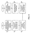
Fig. 6 is a flow diagram describing standalone self-testing of the
single-chip multi-sublayer PHY of Fig. 2 through a first wraparound
test path in accordance with an embodiment of the present invention.
Fig. 7 is a block diagram of an exemplary configuration for
standalone self-testing of the single-chip multi-sublayer PHY of Fig. 2
through a second wraparound test path in accordance with an
embodiment of the present invention.
Fig. 8 is a flow diagram describing standalone self-testing of the
single-chip multi-sublayer PHY of Fig. 2 through a second wraparound
test path in accordance with an embodiment of the present invention.
DETAILED DESCRIPTION OF THE INVENTION
Fig. 1 is a schematic block diagram illustrating certain
components of a 10 Gigabit transceiver module 5 with a XAUI (10
Gigabit attachment unit interface) 15 in accordance with an
embodiment of the present invention. The transceiver module 5 may,
in one embodiment of the present invention, be compatible with the
XENPAK (XAUI module specification) optical module standard. The
transceiver module 5 may, in another embodiment of the present
invention, be compatible with the XPAK (second generation to XENPAK
specification) optical module standard. The transceiver module 5
includes, for example, a single-chip multi-sublayer PHY (physical
layer) 10 also known herein as the transceiver chip 10, an optical PMD
(physical media dependent) 30, and an EEPROM 40.
According to an embodiment of the present invention, a media
access controller (MAC) 20 interfaces to the single-chip multi-sublayer
PHY 10 through the XAUI transmit and receive interface 15. In
general, the MAC layer is one of two sublayers of the data link control
layer and is concerned with sharing the physical connection to a
network among several upper-level systems (e.g. computer systems).
The single-chip multi-sublayer PHY 10 interfaces to the optical PMD
30 through a PMD transmit and receive interface 17. The MAC 20 also
interfaces to the single-chip multi-sublayer PHY 10 through the serial
MDIO (management data input/output) interface 16. The single-chip
multi-sublayer PHY 10 also interfaces to EEPROM 40 through a two-wire
serial interface 19. A separate XGMII (10 Gigabit media
independent interface) is not needed.
The XAUI interface 15 includes 4 channels of 3 Gigabit serial
data received by the single-chip multi-sublayer PHY 10 from the MAC
20 and 4 channels of 3 Gigabit serial data transmitted from the single-chip
multi-sublayer PHY 10 to the MAC 20. In an embodiment of the
present invention, the MAC includes a XGXS (Gigabit media
independent interface extender) sublayer interface and a reconciliation
sublayer (RS) interface. In one embodiment of the present invention,
for Ethernet operation, the 3 Gigabit data rate is actually 3.125 Gbps
and for Fibre Channel operation, the 3 Gigabit data rate is actually
3.1875 Gbps.
The PMD interface 17 includes a 10 Gigabit serial transmit
differential interface and a 10 Gigabit serial receive differential
interface between the single-chip multi-sublayer PHY 10 and the
optical PMD 30 in accordance with an embodiment of the present
invention. In one embodiment of the present invention, for Ethernet
operation, the 10 Gigabit data rate is actually 10.3125 Gbps and for
Fibre Channel operation, the 10 Gigabit data rate is actually 10.5188
Gbps.
Fig. 2 is a schematic block diagram of the single-chip multi-sublayer
PHY 10 used in the transceiver module 5 of Fig. 1 in
accordance with an embodiment of the present invention. The single-chip
multi-sublayer PHY 1 0 includes a PMD transmit (TX) section 110,
a PMD receive (RX) section 120, a digital core section 130, a XAUI
transmit (TX) section 140, and a XAUI receive (RX) section 1 50.
Fig. 3 is a more detailed schematic block diagram of the single-chip
multi-sublayer PHY 10 of Fig. 2 used in the transceiver module 5
of Fig. 1 in accordance with an embodiment of the present invention.
The single-chip multi-sublayer PHY 10 comprises three main
functional paths including a transmit path 310, a receive path 320,
and a management and control path 330. The single-chip multi-sublayer
PHY 10 supports asynchronous clocking mode operation of
the XAUI and PMD interfaces. Clock interfaces are provided for
configuring the XAUI and PMD interfaces to asynchronous or
independent asynchronous operations in accordance with an
embodiment of the present invention. The local reference clock or
external transmit VCXO may adhere to the IEEE specifications.
In the asynchronous mode, elastic FIFOs are used that
accommodate a frequency difference of up to 200 ppm between a
recovered clock and a local reference clock. Both the RX and TX data
paths 310 and 320 contain an elastic FIFO. Idle columns of four bytes
are inserted or deleted during the inter packet gap (IPG) once the
distance between the elastic FIFO's read and write pointers exceed a
threshold. In addition, a column of sequence orders may be deleted
during the IPG once the distance between the elastic FIFO's read and
write pointer exceed a threshold. The delete adjustments occur on IPG
streams that contain at least two columns of idles or sequence order
sets.
Therefore, the Elastic FIFO is enabled to accommodate frequency
differences between the XAUI CDR (clock data recovery) clock and the
PMD CMU (clock multiplier unit) clock (external reference clock), and
differences between the PMD CDR (clock data recovery) clock and the
XAUI CMU clock (external reference clock).
The data transmitted/received is formatted in accordance with a
known protocol, such as the open systems interconnection (OSI) model
(ISO standard). The ISO standard places data into packets including
seven distinct and hierarchical functional layers, known as headers,
followed by the data. The functional layers include a data link layer
and a physical layer. The data link layer and the physical layer are
considered the two lowest level layers of the seven functional layers.
The upper level computer systems build the five highest functional
layers for data packets which are to be transmitted over the optical
network.
The data link layer is associated with the media access controller
(MAC) 20 which is interfaced to the upper level computer system by a
MAC interface 115. The standard MAC data rate for 10 Gigabit
operation is about 10 Gbps. The physical layer for each packet is built
by the transceiver module 5.
Data packets received by the transceiver module 5 include each
of the seven functional layers. The transceiver module 5 examines the
physical layer of data packets and uses the data in the physical layer to
decode the data packets. The MAC 20 examines the data link layer of
data packets and uses the data in the data link layer to decode the
data packets.
The MAC 20 and the single chip multi-sublayer PHY 10 transmit
data therebetween using an interface known as the 10 Gbps Ethernet
Attachment Unit Interface (XAUI) 15. The XAUI is a low pin count, self-clocked
bus directly evolved from lower data rate protocols and is
used for 10G operation. The XAUI is arranged as two, 4-channel
interfaces, each with four serial lines, thereby achieving about 10 Gbps
throughput. One XAUI interface 15A transmits data from the MAC 20
to the single-chip multi-sublayer PHY 10, while the other XAUI
interface 15B transmits data from the single-chip multi-sublayer PHY
10 to the MAC 20.
The single chip multi-sublayer PHY 10 (transceiver chip) is a
fully integrated serialization/deserialization interface device. The
single chip multi-sublayer PHY 10 serializes the data received over the
4-channel XAUI interface 15A and transmits the data as a single 10
Gbps stream to the optical PMD 30. The single chip multi-sublayer
PHY 10 also deserializes a single 10 Gbps signal from the optical PMD
30 and transmits the data as, for example, 4-channels x 3.125 Gbps
over XAUI interface 15B.
Data is received from and transmitted to the optical network via
the optical PMD 30. The optical PMD 30 includes an optical
transmitter 30A and an optical receiver 30B. The optical transmitter
30A transmits data from the computer system over the optical
network. The optical receiver 30B receives data from the optical
network and transmits the data to the computer system. The optical
PMD 30 also acts as an electrical/optical interface. Electrical signals
are received at optical transmitter 30A and transmitted as optical
signals over the optical networks while the optical signals are received
at optical receiver 30B and transmitted as electrical signals to the
computer system.
The single-chip multi-sublayer PHY 10 supports standalone
built in self-testing through two different wraparound test paths in
accordance with an embodiment of the present invention. A first
wraparound test path includes an elastic FIFO 401 of a transmit path
310 of the transceiver chip 10, and a second wraparound test path
includes an elastic FIFO 402 of a receive path 320 of the transceiver
chip 10. Test packets are wrapped around through a test fixture that
connects the inputs and outputs of the XAUI interface 15 of the
transceiver chip 10 and the inputs and outputs of the PMD interface 17
of the transceiver chip 10. In accordance with an embodiment of the
present invention, the test fixture is a simple circuit board that allows
power to be supplied to the transceiver chip 10 and electrically loops
back the test packets over the XAUI interface 1 5 and the PMD interface
17. In other embodiments of the present invention, the test fixture
may be more complex and include, for example, an optical loopback
circuit for the PMD interface 17.
Referring to Fig. 4, for the first wraparound test path, the digital
core 130 includes a packet generator 131 and a packet checker 132.
The packet generator 131 and the packet checker 132 allow
standalone built-in self testing of the single-chip multi-sublayer PHY
10 in accordance with an embodiment of the present invention (also
see Fig. 3).
Referring now to Fig. 5, there is illustrated a block diagram
describing an exemplary test packet stream 300 which may be
generated by the packet generator 131, in accordance with one
embodiment of the present invention. The test packet stream 300
includes any number of test packets 305 and interpacket gaps (IPG)
310 inserted between the test packets 305. The test packets 305
include a start of packet sequence 305a, followed by a header 305b, a
data portion 305c, and an end of packet sequence 305d. The data
portion 305c may comprise sequential data or pseudo-random data.
To test frequency offset under stress conditions, the IPG size
may be sequentially varied during testing from 4 idle bytes to 8 idle
bytes to 12 idle bytes to 16 idle bytes to 20 idle bytes and back to 4
idle bytes (repeating) for an average minimum IPG of 12 idle bytes as
specified in IEEE 802.3ae.
Referring to the flow diagram of Fig. 6 and to Fig. 1 and Fig. 3,
in step 510, the packet generator 131 generates test packets that are
transmitted through a first half of the receive path 320 from point E to
point A to the XAUI output interface 15B. In step 520, the test packets
are electrically wrapped around on the XAUI interface side 15 of the
transceiver chip 10 into the transmit path 310 of the transceiver chip
10. In step 530, the test packets go through the transmit path 310
from point B to point G through the elastic FIFO 401 to point D and to
the PMD output interface 17A. In step 540, the test packets are
electrically wrapped around on the PMD interface side 17 of the
transceiver chip 10 from the transmit path 310 to the receive path
320. In step 550, the test packets go through the second half of the
receive path 320 through point C and then are received at the packet
checker 132 at point F. The packet checker 132 maintains a copy of
the test packets, known as the expected packets. Finally, in step 560,
the packet checker 132 compares the test packets received, from the
wrapping around process, to the expected packets. The transceiver
chip 10 is defective if the received test packets are inconsistent with
the expected packets. For the first wraparound test path, the only part
of the chip not tested is the elastic FIFO 402 in the receive path 320.
Referring again to Fig. 3, there is illustrated an exemplary
single-chip multi-sublayer PHY 10, in accordance with one
embodiment of the present invention. The packet generator 131 for
testing of the first wraparound test path may be incorporated onto
receive path 320 at randomizer 135 (point E) while the packet checker
132 for testing of the first wraparound test path may be incorporated
onto receive path 320 at 64B/66B Synchronizer Descrambler Decoder
134 (point F).
As an alternative, packet checker 136 may be used as well
during testing of the first wrap around test path to allow further
isolation of any defective region of the chip.
As a further alternative, the XAUI and/or PMD TX and RX
sections (110, 120, 140, and 150) may be bypassed. Instead of
looping around the external interfaces through a test fixture, looping
may be done internally around the digital core along internal paths
145 and 146 around digital core 130 as shown in Fig. 4. Such internal
looping back may provide further fault isolation.
Referring to Fig. 7, for the second wraparound test path, the
digital core 130 includes a packet generator 137 and a packet checker
136. The packet generator 137 and the packet checker 136 allow
standalone built-in self testing of the single-chip multi-sublayer PHY
10 in accordance with an embodiment of the present invention (also
see Fig. 3).
Referring to the flow diagram of Fig. 8 and to Fig. 3, in step 610,
the packet generator 137 generates test packets that are transmitted
through a first half of the transmit path 310 from point H to point D to
the PMD output interface 17A. In step 620, the test packets are
electrically wrapped around on the PMD interface side 17 of the
transceiver chip 10 into the receive path 320 of the transceiver chip
10. In step 630, the test packets go through the receive path 320
through point C, through the elastic FIFO 402 to point A, and to XAUI
output interface 15B. In step 640, the test packets are electrically
wrapped around on the XAUI interface side 15 of the transceiver chip
10 from the receive path 320 to the transmit path 310. In step 650,
the test packets go through the second half of the transmit path 310
to point B and to point G and may then be received at the packet
checker 136. The packet checker 136 maintains a copy of the test
packets, known as the expected packets. In step 660, the packet
checker 136 compares the test packets received, in the wrap around
process, to the expected packets. The transceiver chip 10 is defective
if the received test packets are inconsistent with the expected packets.
For the second wraparound test path, the only part of the chip not
tested is the elastic FIFO 401 in the transmit path 310.
Referring again to Fig. 3, the packet generator 137, for testing
the second wraparound test path, may be incorporated onto transmit
path 310 at 64B/66B Encoder Scrambler 133 (point H) while the packet
checker 136 for testing the second wraparound test path may be
incorporated onto transmit path 310 at lane alignment FIFO 308 (point
G).
As an alternative, packet checker 132 may be used as well
during testing of the second wrap around test path to allow further
isolation of any defective region of the chip.
Again, as a further alternative, the XAUI and/or PMD TX and RX
sections (110, 120, 140, and 150) may be bypassed. Instead of
looping around the external interfaces through a test fixture, looping
may be done internally around the digital core along internal paths
145 and 146 around digital core 130 as shown in Fig. 4. Such internal
looping back may provide further fault isolation.
By testing both the first and second wraparound test paths, the
entire transceiver chip 10 is self-tested. In fact, the vast majority of
the transceiver chip 10 is effectively tested twice.
As an alternative, the packet generators and packet checkers
may be located at various other places within the transceiver chip 10.
As a further alternative, the PMD interface side 17 may be wrapped
around through an optical loop such as through an optical PMD,
instead of being looped back electrically.
In summary, certain embodiments of the present invention
provide a system and method for standalone built-in self-testing of a
transceiver chip. The transceiver chip includes packet generators for
providing test packets and packet checkers for comparing received
packets with expected packets. The transceiver chip may be
configured for testing through two wraparound test paths - a first
wraparound test path that includes an elastic FIFO of a transmit path
of the transceiver chip, and a second wraparound test path that
includes an elastic FIFO of a receive path of the transceiver chip.
While the invention has been described with reference to certain
embodiments, it will be understood by those skilled in the art that
various changes may be made and equivalents may be substituted
without departing from the scope of the invention. In addition, many
modifications may be made to adapt a particular situation or material
to the teachings of the invention without departing from its scope.
Therefore, it is intended that the invention not be limited to the
particular embodiment disclosed, but that the invention will include all
embodiments falling within the scope of the appended claims.