EP1407883A1 - Monolithic ink-jet printhead with ink chamber defined by barrier wall and manufacturing method thereof - Google Patents
Monolithic ink-jet printhead with ink chamber defined by barrier wall and manufacturing method thereof Download PDFInfo
- Publication number
- EP1407883A1 EP1407883A1 EP20030256419 EP03256419A EP1407883A1 EP 1407883 A1 EP1407883 A1 EP 1407883A1 EP 20030256419 EP20030256419 EP 20030256419 EP 03256419 A EP03256419 A EP 03256419A EP 1407883 A1 EP1407883 A1 EP 1407883A1
- Authority
- EP
- European Patent Office
- Prior art keywords
- ink
- substrate
- layer
- forming
- nozzle
- Prior art date
- Legal status (The legal status is an assumption and is not a legal conclusion. Google has not performed a legal analysis and makes no representation as to the accuracy of the status listed.)
- Granted
Links
- 230000004888 barrier function Effects 0.000 title claims abstract description 84
- 238000004519 manufacturing process Methods 0.000 title claims abstract description 24
- 239000000758 substrate Substances 0.000 claims abstract description 128
- 239000000463 material Substances 0.000 claims abstract description 52
- 239000004020 conductor Substances 0.000 claims abstract description 50
- 238000005530 etching Methods 0.000 claims abstract description 29
- 230000000149 penetrating effect Effects 0.000 claims abstract description 13
- 238000002161 passivation Methods 0.000 claims description 94
- 238000000034 method Methods 0.000 claims description 47
- 229910052751 metal Inorganic materials 0.000 claims description 31
- 239000002184 metal Substances 0.000 claims description 31
- PXHVJJICTQNCMI-UHFFFAOYSA-N Nickel Chemical compound [Ni] PXHVJJICTQNCMI-UHFFFAOYSA-N 0.000 claims description 18
- 238000009713 electroplating Methods 0.000 claims description 18
- 239000011810 insulating material Substances 0.000 claims description 15
- 239000010931 gold Substances 0.000 claims description 14
- 238000000151 deposition Methods 0.000 claims description 13
- 238000001020 plasma etching Methods 0.000 claims description 13
- PCHJSUWPFVWCPO-UHFFFAOYSA-N gold Chemical compound [Au] PCHJSUWPFVWCPO-UHFFFAOYSA-N 0.000 claims description 12
- 229910052737 gold Inorganic materials 0.000 claims description 12
- VYPSYNLAJGMNEJ-UHFFFAOYSA-N Silicium dioxide Chemical compound O=[Si]=O VYPSYNLAJGMNEJ-UHFFFAOYSA-N 0.000 claims description 11
- XUIMIQQOPSSXEZ-UHFFFAOYSA-N Silicon Chemical compound [Si] XUIMIQQOPSSXEZ-UHFFFAOYSA-N 0.000 claims description 11
- 229920002120 photoresistant polymer Polymers 0.000 claims description 11
- 229910052710 silicon Inorganic materials 0.000 claims description 11
- 239000010703 silicon Substances 0.000 claims description 11
- 229910052814 silicon oxide Inorganic materials 0.000 claims description 11
- 229910052581 Si3N4 Inorganic materials 0.000 claims description 10
- 239000010949 copper Substances 0.000 claims description 10
- HQVNEWCFYHHQES-UHFFFAOYSA-N silicon nitride Chemical compound N12[Si]34N5[Si]62N3[Si]51N64 HQVNEWCFYHHQES-UHFFFAOYSA-N 0.000 claims description 10
- 239000007769 metal material Substances 0.000 claims description 9
- RYGMFSIKBFXOCR-UHFFFAOYSA-N Copper Chemical compound [Cu] RYGMFSIKBFXOCR-UHFFFAOYSA-N 0.000 claims description 8
- 229910052802 copper Inorganic materials 0.000 claims description 8
- 238000010438 heat treatment Methods 0.000 claims description 8
- 229910052759 nickel Inorganic materials 0.000 claims description 8
- 229910000838 Al alloy Inorganic materials 0.000 claims description 7
- 229910052782 aluminium Inorganic materials 0.000 claims description 4
- XAGFODPZIPBFFR-UHFFFAOYSA-N aluminium Chemical compound [Al] XAGFODPZIPBFFR-UHFFFAOYSA-N 0.000 claims description 4
- 229910052709 silver Inorganic materials 0.000 claims description 4
- 239000004332 silver Substances 0.000 claims description 4
- 238000001312 dry etching Methods 0.000 claims description 3
- 238000005498 polishing Methods 0.000 claims description 3
- 239000000126 substance Substances 0.000 claims description 3
- 238000007747 plating Methods 0.000 claims description 2
- 229920000642 polymer Polymers 0.000 claims description 2
- 238000007639 printing Methods 0.000 abstract description 10
- 239000000976 ink Substances 0.000 description 235
- 230000008569 process Effects 0.000 description 11
- 230000007246 mechanism Effects 0.000 description 7
- 230000017525 heat dissipation Effects 0.000 description 6
- 230000005499 meniscus Effects 0.000 description 6
- BOTDANWDWHJENH-UHFFFAOYSA-N Tetraethyl orthosilicate Chemical compound CCO[Si](OCC)(OCC)OCC BOTDANWDWHJENH-UHFFFAOYSA-N 0.000 description 4
- 230000008901 benefit Effects 0.000 description 4
- 238000009413 insulation Methods 0.000 description 4
- WGTYBPLFGIVFAS-UHFFFAOYSA-M tetramethylammonium hydroxide Chemical compound [OH-].C[N+](C)(C)C WGTYBPLFGIVFAS-UHFFFAOYSA-M 0.000 description 4
- NRTOMJZYCJJWKI-UHFFFAOYSA-N Titanium nitride Chemical compound [Ti]#N NRTOMJZYCJJWKI-UHFFFAOYSA-N 0.000 description 3
- RVSGESPTHDDNTH-UHFFFAOYSA-N alumane;tantalum Chemical compound [AlH3].[Ta] RVSGESPTHDDNTH-UHFFFAOYSA-N 0.000 description 3
- 239000012535 impurity Substances 0.000 description 3
- 238000000059 patterning Methods 0.000 description 3
- 229910021420 polycrystalline silicon Inorganic materials 0.000 description 3
- 229920005591 polysilicon Polymers 0.000 description 3
- 238000004544 sputter deposition Methods 0.000 description 3
- MZLGASXMSKOWSE-UHFFFAOYSA-N tantalum nitride Chemical compound [Ta]#N MZLGASXMSKOWSE-UHFFFAOYSA-N 0.000 description 3
- 239000010936 titanium Substances 0.000 description 3
- WQJQOUPTWCFRMM-UHFFFAOYSA-N tungsten disilicide Chemical compound [Si]#[W]#[Si] WQJQOUPTWCFRMM-UHFFFAOYSA-N 0.000 description 3
- 229910021342 tungsten silicide Inorganic materials 0.000 description 3
- VYZAMTAEIAYCRO-UHFFFAOYSA-N Chromium Chemical compound [Cr] VYZAMTAEIAYCRO-UHFFFAOYSA-N 0.000 description 2
- RTAQQCXQSZGOHL-UHFFFAOYSA-N Titanium Chemical compound [Ti] RTAQQCXQSZGOHL-UHFFFAOYSA-N 0.000 description 2
- 230000015572 biosynthetic process Effects 0.000 description 2
- 238000005229 chemical vapour deposition Methods 0.000 description 2
- 230000008021 deposition Effects 0.000 description 2
- 238000004518 low pressure chemical vapour deposition Methods 0.000 description 2
- 238000000623 plasma-assisted chemical vapour deposition Methods 0.000 description 2
- 230000009467 reduction Effects 0.000 description 2
- 229910052719 titanium Inorganic materials 0.000 description 2
- 229910014263 BrF3 Inorganic materials 0.000 description 1
- OAICVXFJPJFONN-UHFFFAOYSA-N Phosphorus Chemical compound [P] OAICVXFJPJFONN-UHFFFAOYSA-N 0.000 description 1
- KWYUFKZDYYNOTN-UHFFFAOYSA-M Potassium hydroxide Chemical compound [OH-].[K+] KWYUFKZDYYNOTN-UHFFFAOYSA-M 0.000 description 1
- 230000008859 change Effects 0.000 description 1
- 239000011248 coating agent Substances 0.000 description 1
- 238000000576 coating method Methods 0.000 description 1
- 239000013078 crystal Substances 0.000 description 1
- 230000007423 decrease Effects 0.000 description 1
- 238000010292 electrical insulation Methods 0.000 description 1
- 238000007641 inkjet printing Methods 0.000 description 1
- 238000001459 lithography Methods 0.000 description 1
- 230000002093 peripheral effect Effects 0.000 description 1
- 239000011574 phosphorus Substances 0.000 description 1
- 229910052698 phosphorus Inorganic materials 0.000 description 1
- 239000004065 semiconductor Substances 0.000 description 1
- 238000000926 separation method Methods 0.000 description 1
- FQFKTKUFHWNTBN-UHFFFAOYSA-N trifluoro-$l^{3}-bromane Chemical compound FBr(F)F FQFKTKUFHWNTBN-UHFFFAOYSA-N 0.000 description 1
- 238000001039 wet etching Methods 0.000 description 1
- IGELFKKMDLGCJO-UHFFFAOYSA-N xenon difluoride Chemical compound F[Xe]F IGELFKKMDLGCJO-UHFFFAOYSA-N 0.000 description 1
Images


Classifications
-
- B—PERFORMING OPERATIONS; TRANSPORTING
- B41—PRINTING; LINING MACHINES; TYPEWRITERS; STAMPS
- B41J—TYPEWRITERS; SELECTIVE PRINTING MECHANISMS, i.e. MECHANISMS PRINTING OTHERWISE THAN FROM A FORME; CORRECTION OF TYPOGRAPHICAL ERRORS
- B41J2/00—Typewriters or selective printing mechanisms characterised by the printing or marking process for which they are designed
- B41J2/22—Typewriters or selective printing mechanisms characterised by the printing or marking process for which they are designed characterised by selective application of impact or pressure on a printing material or impression-transfer material
- B41J2/23—Typewriters or selective printing mechanisms characterised by the printing or marking process for which they are designed characterised by selective application of impact or pressure on a printing material or impression-transfer material using print wires
- B41J2/235—Print head assemblies
-
- B—PERFORMING OPERATIONS; TRANSPORTING
- B41—PRINTING; LINING MACHINES; TYPEWRITERS; STAMPS
- B41J—TYPEWRITERS; SELECTIVE PRINTING MECHANISMS, i.e. MECHANISMS PRINTING OTHERWISE THAN FROM A FORME; CORRECTION OF TYPOGRAPHICAL ERRORS
- B41J2/00—Typewriters or selective printing mechanisms characterised by the printing or marking process for which they are designed
- B41J2/005—Typewriters or selective printing mechanisms characterised by the printing or marking process for which they are designed characterised by bringing liquid or particles selectively into contact with a printing material
- B41J2/01—Ink jet
- B41J2/135—Nozzles
- B41J2/16—Production of nozzles
- B41J2/1621—Manufacturing processes
- B41J2/164—Manufacturing processes thin film formation
- B41J2/1643—Manufacturing processes thin film formation thin film formation by plating
-
- B—PERFORMING OPERATIONS; TRANSPORTING
- B41—PRINTING; LINING MACHINES; TYPEWRITERS; STAMPS
- B41J—TYPEWRITERS; SELECTIVE PRINTING MECHANISMS, i.e. MECHANISMS PRINTING OTHERWISE THAN FROM A FORME; CORRECTION OF TYPOGRAPHICAL ERRORS
- B41J2/00—Typewriters or selective printing mechanisms characterised by the printing or marking process for which they are designed
- B41J2/005—Typewriters or selective printing mechanisms characterised by the printing or marking process for which they are designed characterised by bringing liquid or particles selectively into contact with a printing material
- B41J2/01—Ink jet
- B41J2/135—Nozzles
- B41J2/14—Structure thereof only for on-demand ink jet heads
- B41J2/14016—Structure of bubble jet print heads
- B41J2/14032—Structure of the pressure chamber
-
- B—PERFORMING OPERATIONS; TRANSPORTING
- B41—PRINTING; LINING MACHINES; TYPEWRITERS; STAMPS
- B41J—TYPEWRITERS; SELECTIVE PRINTING MECHANISMS, i.e. MECHANISMS PRINTING OTHERWISE THAN FROM A FORME; CORRECTION OF TYPOGRAPHICAL ERRORS
- B41J2/00—Typewriters or selective printing mechanisms characterised by the printing or marking process for which they are designed
- B41J2/005—Typewriters or selective printing mechanisms characterised by the printing or marking process for which they are designed characterised by bringing liquid or particles selectively into contact with a printing material
- B41J2/01—Ink jet
- B41J2/135—Nozzles
- B41J2/16—Production of nozzles
- B41J2/1601—Production of bubble jet print heads
- B41J2/1603—Production of bubble jet print heads of the front shooter type
-
- B—PERFORMING OPERATIONS; TRANSPORTING
- B41—PRINTING; LINING MACHINES; TYPEWRITERS; STAMPS
- B41J—TYPEWRITERS; SELECTIVE PRINTING MECHANISMS, i.e. MECHANISMS PRINTING OTHERWISE THAN FROM A FORME; CORRECTION OF TYPOGRAPHICAL ERRORS
- B41J2/00—Typewriters or selective printing mechanisms characterised by the printing or marking process for which they are designed
- B41J2/005—Typewriters or selective printing mechanisms characterised by the printing or marking process for which they are designed characterised by bringing liquid or particles selectively into contact with a printing material
- B41J2/01—Ink jet
- B41J2/135—Nozzles
- B41J2/16—Production of nozzles
- B41J2/1621—Manufacturing processes
- B41J2/1626—Manufacturing processes etching
- B41J2/1628—Manufacturing processes etching dry etching
-
- B—PERFORMING OPERATIONS; TRANSPORTING
- B41—PRINTING; LINING MACHINES; TYPEWRITERS; STAMPS
- B41J—TYPEWRITERS; SELECTIVE PRINTING MECHANISMS, i.e. MECHANISMS PRINTING OTHERWISE THAN FROM A FORME; CORRECTION OF TYPOGRAPHICAL ERRORS
- B41J2/00—Typewriters or selective printing mechanisms characterised by the printing or marking process for which they are designed
- B41J2/005—Typewriters or selective printing mechanisms characterised by the printing or marking process for which they are designed characterised by bringing liquid or particles selectively into contact with a printing material
- B41J2/01—Ink jet
- B41J2/135—Nozzles
- B41J2/16—Production of nozzles
- B41J2/1621—Manufacturing processes
- B41J2/1632—Manufacturing processes machining
-
- B—PERFORMING OPERATIONS; TRANSPORTING
- B41—PRINTING; LINING MACHINES; TYPEWRITERS; STAMPS
- B41J—TYPEWRITERS; SELECTIVE PRINTING MECHANISMS, i.e. MECHANISMS PRINTING OTHERWISE THAN FROM A FORME; CORRECTION OF TYPOGRAPHICAL ERRORS
- B41J2/00—Typewriters or selective printing mechanisms characterised by the printing or marking process for which they are designed
- B41J2/005—Typewriters or selective printing mechanisms characterised by the printing or marking process for which they are designed characterised by bringing liquid or particles selectively into contact with a printing material
- B41J2/01—Ink jet
- B41J2/135—Nozzles
- B41J2/14—Structure thereof only for on-demand ink jet heads
- B41J2002/1437—Back shooter
-
- Y—GENERAL TAGGING OF NEW TECHNOLOGICAL DEVELOPMENTS; GENERAL TAGGING OF CROSS-SECTIONAL TECHNOLOGIES SPANNING OVER SEVERAL SECTIONS OF THE IPC; TECHNICAL SUBJECTS COVERED BY FORMER USPC CROSS-REFERENCE ART COLLECTIONS [XRACs] AND DIGESTS
- Y10—TECHNICAL SUBJECTS COVERED BY FORMER USPC
- Y10T—TECHNICAL SUBJECTS COVERED BY FORMER US CLASSIFICATION
- Y10T29/00—Metal working
- Y10T29/49—Method of mechanical manufacture
- Y10T29/49002—Electrical device making
- Y10T29/49082—Resistor making
- Y10T29/49083—Heater type
-
- Y—GENERAL TAGGING OF NEW TECHNOLOGICAL DEVELOPMENTS; GENERAL TAGGING OF CROSS-SECTIONAL TECHNOLOGIES SPANNING OVER SEVERAL SECTIONS OF THE IPC; TECHNICAL SUBJECTS COVERED BY FORMER USPC CROSS-REFERENCE ART COLLECTIONS [XRACs] AND DIGESTS
- Y10—TECHNICAL SUBJECTS COVERED BY FORMER USPC
- Y10T—TECHNICAL SUBJECTS COVERED BY FORMER US CLASSIFICATION
- Y10T29/00—Metal working
- Y10T29/49—Method of mechanical manufacture
- Y10T29/49002—Electrical device making
- Y10T29/49117—Conductor or circuit manufacturing
- Y10T29/49124—On flat or curved insulated base, e.g., printed circuit, etc.
- Y10T29/49126—Assembling bases
-
- Y—GENERAL TAGGING OF NEW TECHNOLOGICAL DEVELOPMENTS; GENERAL TAGGING OF CROSS-SECTIONAL TECHNOLOGIES SPANNING OVER SEVERAL SECTIONS OF THE IPC; TECHNICAL SUBJECTS COVERED BY FORMER USPC CROSS-REFERENCE ART COLLECTIONS [XRACs] AND DIGESTS
- Y10—TECHNICAL SUBJECTS COVERED BY FORMER USPC
- Y10T—TECHNICAL SUBJECTS COVERED BY FORMER US CLASSIFICATION
- Y10T29/00—Metal working
- Y10T29/49—Method of mechanical manufacture
- Y10T29/49002—Electrical device making
- Y10T29/49117—Conductor or circuit manufacturing
- Y10T29/49124—On flat or curved insulated base, e.g., printed circuit, etc.
- Y10T29/49128—Assembling formed circuit to base
-
- Y—GENERAL TAGGING OF NEW TECHNOLOGICAL DEVELOPMENTS; GENERAL TAGGING OF CROSS-SECTIONAL TECHNOLOGIES SPANNING OVER SEVERAL SECTIONS OF THE IPC; TECHNICAL SUBJECTS COVERED BY FORMER USPC CROSS-REFERENCE ART COLLECTIONS [XRACs] AND DIGESTS
- Y10—TECHNICAL SUBJECTS COVERED BY FORMER USPC
- Y10T—TECHNICAL SUBJECTS COVERED BY FORMER US CLASSIFICATION
- Y10T29/00—Metal working
- Y10T29/49—Method of mechanical manufacture
- Y10T29/49002—Electrical device making
- Y10T29/49117—Conductor or circuit manufacturing
- Y10T29/49124—On flat or curved insulated base, e.g., printed circuit, etc.
- Y10T29/4913—Assembling to base an electrical component, e.g., capacitor, etc.
-
- Y—GENERAL TAGGING OF NEW TECHNOLOGICAL DEVELOPMENTS; GENERAL TAGGING OF CROSS-SECTIONAL TECHNOLOGIES SPANNING OVER SEVERAL SECTIONS OF THE IPC; TECHNICAL SUBJECTS COVERED BY FORMER USPC CROSS-REFERENCE ART COLLECTIONS [XRACs] AND DIGESTS
- Y10—TECHNICAL SUBJECTS COVERED BY FORMER USPC
- Y10T—TECHNICAL SUBJECTS COVERED BY FORMER US CLASSIFICATION
- Y10T29/00—Metal working
- Y10T29/49—Method of mechanical manufacture
- Y10T29/49401—Fluid pattern dispersing device making, e.g., ink jet
Definitions
- the present invention relates to an ink-jet printhead, and more particularly, to a thermally driven monolithic ink-jet printhead in which a nozzle plate is formed integrally with a substrate and a manufacturing method thereof.
- ink-jet printheads print a predetermined color image by ejecting small droplet of printing inks at desired positions on a recording sheet.
- Ink-jet printheads are largely categorized into two types depending on the ink droplet ejection mechanisms: a thermally driven ink-jet printhead in which a heat source is employed to form and expand bubbles in ink causing ink droplets to be ejected, and a piezoelectrically driven ink-jet printhead in which a piezoelectric crystal bends to exert pressure on ink causing ink droplets to be expelled.
- the thermally driven ink-jet printing can be further subdivided into top-shooting, side-shooting, and back-shooting types depending on the direction of ink droplet ejection and the directions in which bubbles expand.
- top shooting type refers to a mechanism in which an ink droplet is ejected in the same direction that a bubble expands
- back-shooting type is a mechanism in which an ink droplet is ejected in the opposite direction that a bubble expands.
- the side-shooting type the direction of ink droplet ejection is perpendicular to the direction of bubble expansion.
- Thermally driven ink-jet printheads need to meet the following conditions. First, a simple manufacturing process, low manufacturing cost, and mass production must be allowed. Second, to produce high quality color images, a spacing between adjacent nozzles must be as small as possible while preventing cross-talk between the adjacent nozzles. That is, to increase the number of dots per inch (DPI), many nozzles must be arranged with in a small area. Third, for high speed printing, a cycle beginning with ink ejection and ending with ink refill must be as short as possible. That is, the heated ink and heater should cool down quickly so as to increase an operating frequency.
- DPI dots per inch
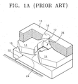
- FIG. 1A is a partial cross-sectional perspective view showing an example of the structure of a conventional thermally driven printhead disclosed in U. S. Patent No. 4,882,595, and FIG. 1B is a cross-sectional view of the printhead of FIG. 1A for explaining a process of ejecting ink droplets.
- the conventional thermally driven ink-jet printhead includes a substrate 10, a barrier wall 14 disposed on the substrate 10 for limiting an ink chamber 26 filled with ink 29, a heater 12 disposed in the ink chamber 26, and a nozzle plate 18 having a nozzle 16 for ejecting an ink droplet 29'.
- the heater 12 If current pulse is supplied to the heater 12, the heater 12 generates heat to form a bubble 28 in the ink 29 within the ink chamber 26.
- the bubble 28 expands to exert pressure on the ink 29 present in the ink chamber 26, which causes an ink droplet 29' to be expelled through the nozzle 16.
- the ink 29 is introduced from a manifold 22 through an ink feed channel 24 to refill the ink chamber 26.
- the process of manufacturing a conventional top-shooting type ink-jet printhead configured as above involves separately manufacturing the nozzle plate 18 equipped with the nozzle 16 and the substrate 10 having the ink chamber 26 and ink feed channel 24 formed thereon and bonding them to each other. This complicates the manufacturing process and may cause misalignment in bonding the nozzle plate 18 with the substrate 10. Furthermore, since the ink chamber 26, the ink channel 24, and the manifold 22 are arranged on the same plane, there is a restriction on increasing the number of nozzles 16 per unit area, i.e., the density of nozzles 16. This makes it difficult to implement a high printing speed, high resolution ink-jet printhead.
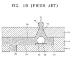
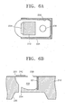
- FIGS. 2A and 2B show an example of a monolithic ink-jet printhead published in U.S. Patent Application No. 20020008738.
- a hemispherical ink chamber 32 and a manifold 36 are formed on the front and rear surfaces of a silicon substrate 30, respectively, and an ink channel 34 connecting the ink chamber 32 with the manifold 36 at the bottom of the ink chamber 32.
- a nozzle plate 40 comprised of a plurality of stacked material layers 41, 42, and 43 is formed integrally with the substrate 30.
- the nozzle plate 40 has a nozzle 47 at a location corresponding to a central portion of the ink chamber 32, and a heater 45 connected to a conductor 46 is disposed around the nozzle 47.
- a nozzle guide 44 extends along the edge of the nozzle 47 toward the ink chamber 32.
- Heat generated by the heater 45 is transferred through an insulating layer 41 to ink 48 within the ink chamber 32.
- the ink 48 then boils to form bubbles 49.
- the created bubbles 49 expands to exert pressure on the ink 48 contained within an ink chamber 32, which causes an ink droplet 48' to be expelled through the nozzle 47.
- the ink 48 is introduced through the ink channel 34 from the manifold 36 due to surface tension of the ink 48 contacting the air to refill the ink chamber 32.
- a conventional monolithic ink-jet printhead configured as above has an advantage in that the silicon substrate 30 is formed integrally with the nozzle plate 40 to allow a simple manufacturing process which eliminates the misalignment problems. Another advantage is that the nozzle 47, the ink chamber 32, the ink channel 34, and the manifold 36 are arranged vertically to increase the density of nozzles 46 as compared with the ink-jet printhead of FIG. 1A.
- the substrate 30 is isotropically etched through the nozzle 47, so that the ink chamber 32 is formed in a hemispherical shape.
- the ink chamber In order to form an ink chamber having a predetermined volume, the ink chamber should have a radius of a predetermined level.
- a reduction in the radius of the ink chamber 32 for the purpose of reducing the spacing between two adjacent nozzles 47 may undesirably result in a reduction in the volume of the ink chamber 32.
- the structure of the conventional monolithic ink-jet printhead has a restriction in realizing high-density nozzle arrangement in spite of recent increasing demand for ink-jet printheads capable of printing higher resolution of images with a high level of DPI (dot per inch).
- the present invention provides a thermally driven monolithic ink-jet printhead capable of printing higher resolution of images by including an ink chamber configured to reduce a spacing between adjacent nozzles.
- the present invention also provides a method of manufacturing the monolithic ink-jet printhead.
- a monolithic ink-jet printhead comprising a substrate having an ink chamber filled with ink to be ejected on its front surface, a manifold for supplying ink to the ink chamber on its rear surface, and an ink channel penetrating between the ink chamber and the manifold, a barrier wall formed on the front surface of the substrate to a predetermined depth and defining at least a part of the ink chamber widthwise, a nozzle plate comprised of a plurality of material layers stacked on the substrate and having a nozzle penetrating the nozzle plate, the nozzle through which ink is ejected from the ink chamber, a heater formed between the material layers of the nozzle plate and located above the ink chamber for heating the ink within the ink chamber, and a conductor provided between the material layers of the nozzle plate and electrically connected to the heater for applying current across the heater.
- the barrier wall preferably surrounds at least a part of the ink chamber so that the ink chamber is formed in a narrow, long shape.
- the barrier wall may surround the ink chamber in a rectangular shape, and one side surface of the barrier wall is preferably rounded.
- the barrier wall is preferably formed of a metal, or an insulating material such as silicon oxide or silicon nitride.
- the nozzle is preferably provided at the widthwise center of the ink chamber, and the heater is preferably located at a position of the nozzle plate above the ink chamber where it may not overlie the nozzle.
- the ink channel may be provided at any location that can connect the ink chamber with the manifold by perpendicularly penetrating the substrate, and the cross-sectional shape of the ink channel is preferably circular, oval, or polygonal.
- the nozzle plate may include a plurality of passivation layers sequentially stacked on the substrate and a heat dissipating layer made of a heat conductive metal for dissipating heat in or around the heater to the outside.
- the plurality of passivation layers include first through third passivation layers sequentially stacked on the substrate, the heater is formed between the first and second passivation layers, and the conductor is located between the second and third passivation layers.
- the heat dissipating layer is preferably made of nickel, copper, or gold, and may be formed by electroplating to a thickness of 10-100 ⁇ m.
- the nozzle plate may have a heat conductive layer located above the ink chamber, insulated from the heater and conductor, and contacting the substrate and heat dissipating layer.
- the heat conductive layer is preferably made of a metal and may be made of the same metal and located on the same passivation layer.
- An insulating layer may be interposed between the conductor and the heat conductive layer.
- a method of manufacturing a monolithic ink-jet printhead comprising (a) preparing a substrate, (b) forming a barrier wall made of a predetermined material different from a material of the substrate, (c) integrally forming a nozzle plate comprised of a plurality of material layers and having a nozzle penetrating the material layers, and forming a heater and a conductor connected to the heater between the material layers, (d) forming an ink chamber defined by the barrier wall by isotropically etching the substrate exposed through the nozzle using the barrier wall as an etch stop, (e) forming a manifold for supplying ink by etching a rear surface of the substrate, and (f) forming an ink channel by etching the substrate so that it penetrates the substrate between the manifold and the ink chamber.
- the substrate is preferably made of a silicon wafer.
- the barrier wall may surround at least a part of the ink chamber so that the ink chamber is formed in a narrow, long shape, and one side surface of the barrier wall is preferably rounded.
- the barrier wall is preferably formed of a metal.
- the step (b) may comprise forming an etch mask defining a portion to be etched on the front surface of the substrate, forming a trench by etching the substrate exposed through the etch mask to a predetermined depth, removing the etch mask, depositing the metal on the front surface of the substrate to fill the trench for forming the barrier wall, and forming a metal material layer made of the metal on the substrate, and removing the metal material layer formed on the substrate.
- the barrier wall may be formed of an insulating material such as silicon oxide or silicon nitride.
- the step (b) may comprise forming an etch mask defining a portion to be etched on the front surface of the substrate, forming a trench by etching the substrate exposed through the etch mask to a predetermined depth, removing the etch mask, and depositing the insulating material on the front surface of the substrate to fill the trench for forming the barrier wall, and forming an insulating material layer made of the insulating material on the substrate.
- the step (c) may comprise (c-1) sequentially stacking a plurality of passivation layers on the substrate and forming the heater and the conductor between the passivation layers, and (c-2) forming a heat dissipating layer made of a metal on the substrate and forming the nozzle so as to penetrate the passivation layers and the heat dissipating layer.
- the step (c-1) may comprises forming a first passivation layer on the substrate, forming the heater on the first passivation layer, forming a second passivation layer on the first passivation layer and the heater, forming the conductor on the second passivation layer, and forming a third passivation layer on the second passivation layer and the conductor.
- the heater is preferably formed in a rectangular shape.
- a heat conductive layer located above the ink chamber, insulated from the heater and conductor, and contacting the substrate and heat dissipating layer is preferably formed between the passivation layers.
- the heat dissipating layer may be formed of nickel, copper, or gold, and is preferably formed by electroplating to a thickness of 10-100 ⁇ m.
- the step (c-2) may comprise etching the passivation layers to form a lower nozzle with a predetermined diameter on a portion where the ink chamber is formed, forming a first sacrificial layer within the lower nozzle, forming a second sacrificial layer for forming an upper nozzle on the first sacrificial layer, forming the heat dissipating layer on the passivation layers by electroplating, and removing the second sacrificial layer and the first sacrificial layer, and forming the complete nozzle consisting of the lower and upper nozzles.
- the lower nozzle is preferably formed by dry etching the passivation layers using reactive ion etching (RIE).
- RIE reactive ion etching
- the second sacrificial layer may be formed.
- the first sacrificial layer and the second sacrificial layer may be formed sequentially or integrally with each other.
- the method may further comprise planarizing the top surface of the heat dissipating layer by chemical mechanical polishing (CMP) after forming the heat dissipating layer.
- CMP chemical mechanical polishing
- step (d) horizontal etching may be stopped and only vertical etching may be performed around the barrier wall due to the presence of the barrier wall serving as an etch stop.
- the substrate may be dry etched by reactive ion etching (RIE) from the rear surface of the substrate on which the manifold has been formed to form the ink channel.
- RIE reactive ion etching
- a narrow, long, deep ink chamber is formed using a barrier wall serving as an etch stop, a spacing between adjacent nozzles can be reduced, thereby realizing an ink-jet printhead capable of printing higher resolution of images with a high level of DPI. Also, since a nozzle plate having a nozzle is formed integrally with a substrate having an ink chamber and an ink channel formed thereon, the ink-jet printhead can be realized on a single wafer in a single process.
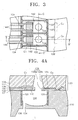
- FIG. 3 partially shows the planar structure of a monolithic ink-jet printhead according to a preferred embodiment of the present invention, illustrating the shape and arrangement of an ink passageway and a heater
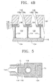
- FIGS. 4A and 4B are vertical cross-sectional views of the ink-jet printhead of the present invention taken along lines B-B' and C-C' of FIG. 3
- FIG. 5 is a plan view showing the planar structure of a heat conductive layer shown in FIG. 4A.
- the ink-jet printhead includes an ink passageway connected from an ink reservoir (not shown) to a manifold 136, an ink channel 134, an ink chamber 132 and to a nozzle 138.
- the manifold 136 is formed at the rear surface of a substrate 110 of the printhead and supplies ink from the ink reservoir to the ink chamber 132.
- the ink chamber 132 is formed on the surface of the substrate 110 and ink to be ejected is filled therein.
- the ink channel 134 is formed so as to perpendicularly penetrate the substrate 110 between the ink chamber 132 and the manifold 136.
- a plurality of ink chambers 132 are arranged on the manifold 136 connected to the ink reservoir in one or two rows, or in three or more rows to achieve higher resolution.
- a plurality of ink channels 134, nozzles 138 and heaters 142, each provided for one ink chamber 132, are also arranged on the manifold 136 in one or more rows.
- a silicon wafer widely used to manufacture integrated circuits (ICs) may be used as the substrate 110.
- the ink chamber 132 is defined by a barrier wall 131.
- the barrier wall 131 is formed on the front surface of the substrate 110 to a predetermined depth in consideration of the depth of the ink chamber 132, for example, several micrometers to several tens micrometers.
- the ink chamber 132 is narrow, long and deep. That is to say, in the embodiment the ink chamber is at least 50% longer, preferably at least twice as long as it is wide. The depth may be in the range several micrometers to several tens of micrometers.
- the ink chamber 132 is capable of accommodating ink enough to eject ink droplets even if it is narrow in a direction in which nozzles are arranged.
- the width of the ink chamber 132 is small, a spacing between adjacent nozzles 138 is reduced, so that a high-density arrangement of the nozzles 138 is allowed, thereby achieving an ink-jet printhead with print resolution of a high level of DPI.
- the rectangular barrier wall 131 surrounding the ink chamber 132 may be separately provided at each of the plurality of the ink chambers 132, and a part of the barrier wall 131 positioned between adjacent ink chambers 132 can be shared by the adjacent ink chambers 132.
- the part of the barrier wall 131 positioned between adjacent ink chambers 132 is as thick as it withstands pressure change in the ink chamber 132, for example, several micrometers.
- the plane surrounded by the barrier wall 131 may take various shapes other than a rectangle, which will later be described.
- the barrier wall 131 is formed of a different material from the substrate 110, which is for allowing the barrier wall 131 to serve as an etch stop in the process of forming the ink chamber 132, which will be described below.
- the barrier wall 131 may be formed of an insulating material such as silicon oxide or silicon nitride, which is advantageous in that the same material can be used for both the barrier wall 131 and a first passivation layer 121 to be described later.
- the barrier wall 131 may be formed of a metal material, which is advantageous in that heat inside the ink chamber 132 can be dissipated through the barrier wall 131 relatively rapidly.
- the ink channel 134 can be formed perpendicularly at a position deviating from the center of the ink chamber 132, that is, at the peripheral portion of the ink chamber 132. Thus, the ink channel 134 is positioned under the heater 142, rather than under the nozzles 138.
- the cross-section of the ink channel 134 is preferably shaped of a rectangle elongated in a width direction of the ink chamber 132.
- the ink channel 134 may have various cross-sectional shapes such as circular, oval or polygonal ones.
- the ink channel 134 may be formed at any location other than under the heater 142 that can connect the ink chamber 132 with the manifold 136 by perpendicularly penetrating the substrate 110.
- a nozzle plate 120 is formed on the substrate 110 having the ink chamber 132, the ink channel 134, and the manifold 136 formed thereon.
- the nozzle plate 120 forming an upper wall of the ink chamber 132 has a nozzle 138, through which ink is ejected.
- the nozzle 138 is formed on the widthwise center of the ink chamber 132 by penetrating the nozzle plate 120 perpendicularly to the nozzle plate 120.
- the nozzle plate 120 is comprised of a plurality of material layers stacked on the substrate 110.
- the plurality of material layers may consist of first, second and third passivation layers 121, 122 and 126.
- the plurality of material layers further include a heat dissipating layer 128 made of a metal.
- the plurality of material layers further include a heat conductive layer 124.
- a heater 142 is provided between the first and second passivation layers 121 and 122, and a conductor 144 is provided between the second and third passivation layers 122 and 126.
- the first passivation layer 121 is formed on top of the substrate 110.
- the first passivation layer 121 for electrical insulation between the overlying heater 142 and underlying substrate 110 as well as protection of the heater 142 may be made of silicon oxide or silicon nitride.
- the first passivation layer 121 and the barrier wall 131 are preferably formed of the same material.
- the heater 142 overlying the ink chamber 132 to heat ink inside the ink chamber 132 is formed on the first passivation layer 121.
- the heater 142 consists of a resistive heating material such as polysilicon doped with impurities, tantalum-aluminum alloy, tantalum nitride, titanium nitride, and tungsten silicide.
- the heater 142 may be rectangular.
- the heater 142 is located at a position above the ink chamber 132 where it may not overlie the nozzle 138, that is, at a location deviating from the center of the ink chamber 132. In other words, since the nozzle 138 is formed at one side in view of the lengthwise center of the ink chamber 132, the heater 142 is disposed at the other side in view of the lengthwise center of the ink chamber 132.
- the second passivation layer 122 is formed on the first passivation layer 121 and the heater 142 for insulation between the overlying heat conductive layer 124 and the underlying heater 142 as well as protection of the heater 142.
- the second passivation layer 122 may be made of silicon nitride and silicon oxide.
- the conductor 144 electrically connected to the heater 142 for applying a current pulse across the heater 142 is placed on the second passivation layer 122. While one end of the conductor 144 is coupled to the heater 142 through a first contact hole C 1 formed in the second passivation layer 122, the other end is electrically connected to a bonding pad (not shown).
- the conductor 144 may be made of a highly conductive metal such as aluminum, aluminum alloy, gold, or silver.
- the heat conductive layer 124 may overlie the second passivation layer 122.
- the heat conductive layer 124 functions to conduct heat residing in or around the heater 142 to the substrate 110 and the heat dissipating layer 128 which will be described later, and is preferably formed as widely as possible to entirely cover the ink chamber 132 and the heater 142, as shown in FIG. 5.
- the heat conductive layer 124 needs to be spaced apart a predetermined distance from the conductor 144 for insulation purpose. The insulation between the heat conductive layer 124 and the conductor 144 can be achieved by the second passivation layer 122 interposed therebetween.
- the heat conductive layer 124 contacts the top surface of the substrate 110 through a second contact hole C 2 penetrating the first and second passivation layers 121 and 122.
- the heat conductive layer 124 is made of a metal having good conductivity.
- the heat conductive layer 124 may be made of the same material as the conductor 144, such as aluminum, aluminum alloy, gold, or silver.
- an insulating layer (not shown) may be provided between the conductor 144 and the heat dissipating layer 124.
- the third passivation layer 126 overlying on the conductor 144 and the second passivation layer 122 may be made of tetraethylorthosilicate (TEOS) oxide or silicon oxide. It is desirable not to form the third passivation layer 126 on the heat conductive layer 124 for contacting the heat conductive layer 124 and the heat dissipating layer 128.
- TEOS tetraethylorthosilicate
- the heat dissipating layer 128, the uppermost layer from among the plurality of material layers forming the nozzle plate 120, is made of a metal having high thermal conductivity such as nickel, copper, or gold.
- the heat dissipating layer 128 is formed as thickly as 10 ⁇ 100 ⁇ m by electroplating the metal on the third passivation layer 126 and the heat conductive layer 124.
- a seed layer 127 for electroplating of the metal is disposed on top of the third passivation layer 126 and the heat conductive layer 124.
- the seed layer 127 may be made of a metal having good electric conductivity such as copper, chrome, titanium, gold or nickel.
- the heat dissipating layer 128 made of a metal as described above is formed by a electroplating process, it can be formed integrally with other components of the ink-jet printhead and relatively thickly, thus providing effective heat dissipation.
- the heat dissipating layer 128 functions to dissipate the heat from the heater 142 or from around the heater 142 to the outside. That is, the heat residing in or around the heater 142 after ink ejection is guided to the substrate 110 and the heat dissipating layer 128 via the heat conductive layer 124 and then dissipates to the outside. This allows quick heat dissipation after ink ejection and lowers the temperature near the nozzle 138, thereby providing a stable printing at a high operating frequency.
- a relatively thick heat dissipating layer 128 as described above makes it possible to sufficiently secure the length of the nozzle 138, which enables stable high speed printing while improving the directionality of an ink droplet being ejected through the nozzle 138. That is, the ink droplet can be ejected in a direction exactly perpendicular to the substrate 110.
- the nozzle 138 consisting of a lower part 138a and an upper part 138b, is formed in and penetrates the nozzle plate 120.
- the lower part 138a of the nozzle 138 is formed in a pillar shape by penetrating the passivation layers 121, 122, and 126 of the nozzle plate 120.
- the upper part 138b of the nozzle 138 is formed in and penetrates the heat dissipating layer 128.
- the upper part 138b of the nozzle 138 may also be formed in a pillar shape.
- the upper part 138b is preferably tapered so that the cross-sectional area becomes smaller toward its exit. If the upper part 138b has a tapered shape as described above, a meniscus in the ink surface is more quickly stabilized after ink ejection.
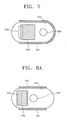
- FIGS. 6A and 6B are a plan view and a cross-sectional view of a barrier wall and an ink chamber in an ink-jet printhead according to another embodiment of the present invention.
- a barrier wall 231 is formed such that it surrounds parts of an ink chamber 232, for example, three sides of the ink chamber 232, inside a substrate 210. Accordingly, the ink chamber 232 defined by the barrier wall 231 is formed in a narrow, long shape. One side of the ink chamber 232 where the barrier wall 231 is not formed, is rounded by isotropically etching the substrate 210.
- the shapes and arrangement of other components of the ink-jet printhead, that is, a heater 242 formed on a first passivation layer 221, a nozzle 238, an ink channel 234 and a manifold 236, are the same as those in the above-described embodiment.
- FIG. 7 is a plan view of a barrier wall and an ink chamber in an ink-jet printhead according to still another embodiment of the present invention.
- the cross-sectional view of the ink-jet printhead shown in FIG. 6 is the same as that shown in FIG. 6B, and an explanation thereof will not be given.
- a barrier wall 331 is formed such that it surrounds parts of an ink chamber 332, for example, three sides of the ink chamber 232.
- One side of the barrier wall 331 may be rounded.
- the ink chamber 332 defined by the barrier wall 331 is formed in a narrow, long shape, as described above.
- the shapes and arrangement of other components of the ink-jet printhead, that is, a heater 342, a nozzle 338 and an ink channel 334, are the same as those in the above-described embodiment.
- FIGS. 8A and 8B are a plan view and a cross-sectional view of a barrier wall and an ink chamber in an ink-jet printhead according to another embodiment of the present invention.
- a barrier wall 431 is separated into two parts at opposite sides of an ink chamber 432 widthwise.
- the barrier wall 431 defines only the width of the ink chamber 432. Accordingly, the ink chamber 432 defined by the barrier wall 431 may be formed in a narrow, long shape. Both lengthwise sides of the ink chamber 432 where the barrier wall 431 is not formed, are rounded by isotropically etching a substrate 410.
- a nozzle 438 is provided at the lengthwise center of the ink chamber 432.
- a heater 442 formed on a first passivation layer 421 may be rectangular.
- the heater 442 may be located at one side of the nozzle 438.
- the heater 442 may also be located at opposite sides of the nozzle 438.
- the heater 442 may be formed such that it surrounds the nozzle 438.
- the shapes and arrangement of other components of the ink-jet printhead, that is, an ink channel 434 and a manifold 436, are the same as those in the above-described embodiment.
- a meniscus in the surface of the ink 150 retreats toward the ink chamber 132 after ink droplet separation.
- the nozzle 138 is sufficiently long due to the thick nozzle plate 120 so that the meniscus retreats only within the nozzle 238 not into the ink chamber 132.
- this prevents air from flowing into the ink chamber 132 while quickly restoring the meniscus to its original state, thereby stably maintaining high speed ejection of the ink droplet 150'.
- heat residing in or around the heater 142 is dissipated into the substrate 110 or to the outside by conduction heat transfer through the heat conductive layer 124 and the heat dissipating layer 128, the temperature in or around the heater 142 and nozzle 138 drops more quickly.
- the barrier wall 131 is made of a metal material, heat dissipation is performed relatively rapidly.
- the ink 150 flows again toward the exit of the nozzle 138 due to a surface tension force acting at a meniscus formed in the nozzle 138. If the upper part 138b of the nozzle 138 is tapered, the speed at which the ink 150 flows upward further increases.
- the ink 150 is then supplied through the ink channel 134 to refill the ink chamber 132.
- the ink ejection mechanism is repeated. During the above process, it can thermally recover its original state more quickly because of heat dissipation through the heat conductive layer 124 and heat dissipating layer 128.
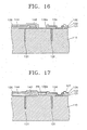
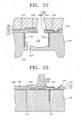
- FIGS. 10 through 22 are cross-sectional views for explaining a method of manufacturing the ink-jet printhead shown in FIG. 3, and FIG. 23 shows another method of forming a seed layer and sacrificial layers. Meanwhile, methods of manufacturing the ink-jet printheads having the nozzle plates shown in FIGS. 6A, 7 and 8A are the same as described below except for the shapes of a barrier wall and an ink chamber.
- a silicon wafer used for the substrate 110 has been processed to have a thickness of approximately 300-500 ⁇ m.
- the silicon wafer is widely used for manufacturing semiconductor devices and effective for mass production.
- FIG. 10 shows a very small portion of the silicon wafer
- the ink-jet printhead according to this invention can be fabricated in tens to hundreds of chips on a single wafer.
- An etch mask 112 that defines a portion to be etched is formed on the surface of the substrate 110.
- the etch mask 112 can be formed by coating a photoresist on the front surface of the substrate 110 and patterning the same.
- the substrate 110 exposed by the etch mask 112 is etched, thereby forming a trench 114 having a predetermined depth.
- the substrate 110 is dry-etched by reactive ion etching (RIE).
- RIE reactive ion etching
- the depth of the trench 114 is determined to be in the range of several micrometers to several tens micrometers in consideration of the depth of the ink chamber (132 of FIG. 21).
- the width of the trench 114 is in the range of several micrometers enough to easily fill a predetermined material therein.
- the trench 114 surrounds a portion where the ink chamber 132 is to be formed in a rectangular shape. In the ink chamber 232, 332 or 432 shown in FIGS.
- the trench 114 may have various shapes adapted to the shape of each ink chamber.
- the trench 114 may surround parts of the ink chamber 232, 332 or 432, and the trench 114 may be rounded partially at the internal surface thereof.
- the etch mask 112 on the substrate 110 is removed.
- a predetermined material is deposited on the surface of the substrate 110 having the trench 114. Accordingly, the trench 114 is filled with the predetermined material, thereby forming the barrier wall 131.
- a material layer 116 is formed on the substrate 110. The predetermined material is different from a material forming the substrate 110. This is for making the barrier wall 131 serve as an etch stop when the ink chamber 132 is formed by etching the substrate 110, as shown in FIG. 21.
- an insulating material such as silicon oxide or silicon nitride, or a metallic material, can be used as the predetermined material, as described above,
- the barrier wall 131 and the material layer 116 are made of an insulating material like the first passivation layer 121 shown in FIG. 12, the material layer 116 can be used as the first passivation layer 121, making it possible to omit the step of separately forming the first passivation layer 121.
- the barrier wall 131 and the material layer 116 are made of a metallic material, the material layer 116 on the substrate 110 is etched for removal, and then steps shown in FIG. 12 are performed.
- the first passivation layer 121 is formed over the substrate 110 having the barrier wall 131.
- the first passivation layer 121 is formed by depositing silicon oxide or silicon nitride on the substrate 110.
- the heater 142 is then formed on the first passivation layer 121 overlying the substrate 110.
- the heater 142 is formed by depositing a resistive heating material, such as polysilicon doped with impurities, tantalum-aluminum alloy, tantalum nitride, titanium nitride, or tungsten silicide, over the entire surface of the first passivation layer 121 to a predetermined thickness and patterning the same in a predetermined shape, e.g., in a rectangular shape.
- a resistive heating material such as polysilicon doped with impurities, tantalum-aluminum alloy, tantalum nitride, titanium nitride, or tungsten silicide
- the polysilicon doped with impurities such as phosphorus (P) -containing a source gas can be deposited by low pressure chemical vapor deposition (LPCVD) to a thickness of approximately 0.7-1 ⁇ m
- LPCVD low pressure chemical vapor deposition
- tantalum-aluminum alloy, tantalum nitride, titanium nitride, or tungsten silicide may be deposited by sputtering or chemical vapor deposition (CVD) to a thickness of about 0.1-0.3 ⁇ m.
- the deposition thickness of the resistive heating material may be determined in a range other than given here to have an appropriate resistance considering the width and length of the heater 142.
- the resistive heating material deposited over the entire surface of the first passivation layer 121 can be patterned by a lithography process using a photomask and a photoresist and an etching process using a photoresist pattern as an etch mask.
- the second passivation layer 122 is formed on the first passivation layer 121 and the heater 142.
- the second passivation layer 122 is formed by depositing silicon oxide or silicon nitride to a thickness of about 0.5 ⁇ m.
- the second passivation layer 122 is then partially etched to form a first contact hole C 1 exposing a portion of the heater 142 to be coupled with the conductor 144 in a step shown in FIG. 14, and the second and first passivation layers 122 and 121 are sequentially etched to form a second contact hole C 2 exposing a portion of the substrate 110 to contact the heat conductive layer 124 in step shown in FIG. 14.
- the first and second contact holes C 1 and C 2 can be formed simultaneously.
- FIG. 14 shows the state in which the conductor 144 and the heat conductive layer 124 have been formed on the second passivation layer 122.
- the conductor 144 and the heat conductive layer 124 can be formed at the same time by depositing a metal having excellent electric and thermal conductivity such as aluminum, aluminum alloy, gold or silver using sputtering techniques to a thickness of the order of 1 ⁇ m and patterning the same.
- the conductor 144 and the heat conductive layer 124 are formed to'insulate each other, so that the conductor 144 is coupled to the heater 142 through the first contact hole C 1 and the heat conductive layer 124 contacts the substrate 110 through the second contact hole C 2 .
- the heat conductive layer 124 can be formed after having formed the conductor 144. More specifically, after forming only the first contact hole C 1 , the conductor 144 is formed. An insulating layer (not shown) is then formed on the conductor 144 and second passivation layer 122. The insulating layer can be formed from the same material using the same method as the second passivation layer 122. The insulating layer and the second and first passivation layers 122 and 121 are then sequentially etched to form the second contact hole C 2 .
- the heat conductive layer 124 is formed.
- the insulating layer is interposed between the conductor 144 and the heat conductive layer 124.
- FIG. 15 shows the state in which the third passivation layer 126 has been formed over the entire surface of the resultant structure of FIG. 14.
- the third passivation layer 126 is formed by depositing tetraethylorthosilicate (TEOS) oxide using plasma enhanced chemical vapor deposition (PECVD) to a thickness of approximately 0.7-3 ⁇ m. Then, the third passivation layer 126 is partially etched to expose the heat conductive layer 124.
- TEOS tetraethylorthosilicate
- PECVD plasma enhanced chemical vapor deposition
- FIG. 16 shows the state in which the lower nozzle 138a has been formed.
- the lower nozzle 138a is formed by sequentially etching the third, second, and first passivation layers 126, 122, and 121 using reactive ion etching (RIE).
- RIE reactive ion etching
- a first sacrificial layer PR 1 is then formed within the lower nozzle 138a.
- a photoresist is applied over the entire surface of the resultant structure of FIG. 16 and patterned to leave only the photoresist filled in the lower nozzle 138a.
- the residual photoresist is used to form the first sacrificial layer PR 1 thus maintaining the shape of the lower nozzle 138a during the subsequent steps.
- a seed layer 127 is formed for electric plating over the entire surface of the resulting structure formed after formation of the first sacrificial layer PR 1 .
- the seed layer 127 is formed on the entire surface of the resultant structure.
- the seed layer 127 may be formed by depositing metal having good conductivity such as copper (Cu), chrome (Cr), titanium (Ti), gold (Au), or nickel (Ni) to a thickness of approximately 500-3,000 A using sputtering techniques.
- FIG. 18 shows the state in which a second sacrificial layer PR 2 for forming the upper nozzle 138b has been formed.
- a photoresist is applied over the entire surface of seed layer 127 and patterned to leave the photoresist only at a portion where the upper nozzle 138a is to be formed as shown in FIG. 20.
- the residual photoresist is formed in a tapered shape whose cross-sectional area decreases toward the top and acts as the second sacrificial layer PR 2 for forming the upper nozzle 138b in the subsequent steps.
- the second sacrificial layer PR 2 is also formed in a pillar-shape.
- the first and second sacrificial layers PR 1 and PR 2 can be made from a photosensitive polymer instead of a photoresist.
- the heat dissipating layer 128 is formed from a metal of a predetermined thickness on top of the seed layer 127.
- the heat dissipating layer 128 can be formed to a thickness of about 10-100 ⁇ m by electroplating nickel (Ni), copper (Cu), or gold (Au) over the surface of the seed layer 127.
- Ni nickel
- Cu copper
- Au gold
- the electroplating process is completed when the heat dissipating layer 128 is formed to a desired height at which the exit section of the upper nozzle 138b is formed, the height being less than that of the second sacrificial layer PR 2 .
- the thickness of the heat dissipating layer 128 may be appropriately determined considering the cross-sectional area and shape of the upper nozzle 138b and heat dissipation capability with respect to the substrate 110 and the outside.
- the surface of the heat dissipating layer 128 that has undergone electroplating has irregularities due to the underlying material layers, it may be planarized by chemical mechanical polishing (CMP).
- CMP chemical mechanical polishing
- the second sacrificial layer PR 2 for forming the upper nozzle 138b, the underlying seed layer 127, and the first sacrificial layer PR 1 for maintaining the lower nozzle 138a are then sequentially etched to form the complete nozzle 138 by connecting the lower and upper nozzles 138a and 138b and the nozzle plate 120 comprised of the plurality of material layers.
- the nozzle 138 and the heat dissipating layer 128 may be formed through the following steps. Referring to FIG. 23 a seed layer 127' for electroplating is formed over the entire surface of the resulting structure of FIG. 16 before forming the first sacrificial layer PR 1 for maintaining the lower nozzle 238a. The first sacrificial layer PR 1 and the second sacrificial layer PR 2 are then sequentially or simultaneously and integrally formed. Next, the heat dissipating layer 128 is formed as shown in FIG. 19, followed by planarization of the surface of the heating dissipating layer 128 by CMP. After the planarization, the second and first sacrificial layers PR 2 and PR 1 , and the underlying seed layer 127' are etched to form the nozzle 138 and nozzle plate 120 as shown in FIG. 20.
- FIG. 21 shows the state in which the ink chamber 132 of a predetermined depth has been formed on a front surface of the substrate 110.
- the ink chamber 132 can be formed by isotropically etching the substrate 110 exposed by the nozzle 138. That is, dry etching is carried out on the substrate 110 using XeF 2 or BrF 3 gas as an etch gas for a predetermined period of time.
- the substrate 110 is isotropically etched, that is, the substrate 110 is etched in every direction from the portion exposed by the nozzle 138 at the same etching rate.
- horizontal etching is stopped at the barrier wall 131 serving as an etch stop, etching is performed at the barrier wall 131 in a vertical direction only.
- the ink chamber 132 surrounded by the barrier wall 131 is formed in a narrow, long, deep shape.
- FIG. 22 shows the state in which the manifold 136 and the ink channel 134 have been formed by etching the substrate 110 from its rear surface.
- an etch mask that limits a region to be etched is formed on the rear surface of the substrate 110, and wet etching is performed using tetramethyl ammonium hydroxide (TMAH) or potassium hydroxide (KOH) as an etchant to form the manifold 136 with an inclined side surface.
- TMAH tetramethyl ammonium hydroxide
- KOH potassium hydroxide
- the manifold 136 may be formed by anisotropically etching the rear surface of the substrate 110.
- an etch mask that defines the ink channel 134 is formed on the rear surface of the substrate 110 where the manifold 136 has been formed, and the substrate 110 between the manifold 136 and ink chamber 132 is dry-etched by RIE thus forming the ink channel 134.
- a monolithic ink-jet printhead according to this invention having the ink chamber 132 defined by the barrier wall 131 is completed, as shown in FIG. 22.
- an ink chamber having various shapes adapted to the shape of a barrier wall can be formed.
- a narrow, long ink chamber is formed, a spacing between adjacent nozzles can be reduced.
- the monolithic ink-jet printhead and the manufacturing method thereof according to this invention have the following advantages.
- a narrow, long, deep ink chamber can be formed by forming a barrier wall serving as an etch stop.
- a spacing between adjacent nozzles can be reduced, thereby realizing an ink-jet printhead capable of printing higher resolution of images with a high level of DPI.
- the degree of freedom is high in the design and manufacture of the ink-jet printhead, thereby easily improving the ink ejection performance and operating frequency.
- this invention improves heat sinking capability due to the presence of a barrier wall made of a metal or a heat dissipation layer made of a thick metal, thereby increasing the ink ejection performance and operating frequency. Also, a sufficient length of the nozzle can be secured so that a meniscus is maintained within the nozzle, thereby allowing stable ink refill operation while increasing the directionality of an ink droplet being ejected.
- this invention can provide an ink-jet printhead on a single wafer using a monolithic process. This eliminates the conventional problems of misalignment between the nozzle and ink chamber, thereby increasing the ink ejection performance and manufacturing yield.
- each element of a printhead may not be limited to those described herein. That is, the substrate may be formed of a material having good processibility, other than silicon, and the same is true of a heater, a conductor, a passivation layer, a heat conductive layer, or a heat dissipating layer.
- the stacking and formation method for each material are only examples, and a variety of deposition and etching techniques may be adopted.
Abstract
Description
- The present invention relates to an ink-jet printhead, and more particularly, to a thermally driven monolithic ink-jet printhead in which a nozzle plate is formed integrally with a substrate and a manufacturing method thereof.
- In general, ink-jet printheads print a predetermined color image by ejecting small droplet of printing inks at desired positions on a recording sheet. Ink-jet printheads are largely categorized into two types depending on the ink droplet ejection mechanisms: a thermally driven ink-jet printhead in which a heat source is employed to form and expand bubbles in ink causing ink droplets to be ejected, and a piezoelectrically driven ink-jet printhead in which a piezoelectric crystal bends to exert pressure on ink causing ink droplets to be expelled.
- An ink ejection mechanism of the thermally driven ink-jet printhead will now be described in detail. When a current pulse is applied to a heater consisting of a resistive heating material, heat is generated from the heater to rapidly heat ink near the heater to approximately 300°C and boil the ink to form bubbles. The formed bubbles expand to exert pressure on ink contained within an ink chamber. This causes a droplet of ink to be ejected through a nozzle from the ink chamber.
- Here, the thermally driven ink-jet printing can be further subdivided into top-shooting, side-shooting, and back-shooting types depending on the direction of ink droplet ejection and the directions in which bubbles expand. While the top shooting type refers to a mechanism in which an ink droplet is ejected in the same direction that a bubble expands, the back-shooting type is a mechanism in which an ink droplet is ejected in the opposite direction that a bubble expands. In the side-shooting type, the direction of ink droplet ejection is perpendicular to the direction of bubble expansion.
- Thermally driven ink-jet printheads need to meet the following conditions. First, a simple manufacturing process, low manufacturing cost, and mass production must be allowed. Second, to produce high quality color images, a spacing between adjacent nozzles must be as small as possible while preventing cross-talk between the adjacent nozzles. That is, to increase the number of dots per inch (DPI), many nozzles must be arranged with in a small area. Third, for high speed printing, a cycle beginning with ink ejection and ending with ink refill must be as short as possible. That is, the heated ink and heater should cool down quickly so as to increase an operating frequency.
- FIG. 1A is a partial cross-sectional perspective view showing an example of the structure of a conventional thermally driven printhead disclosed in U. S. Patent No. 4,882,595, and FIG. 1B is a cross-sectional view of the printhead of FIG. 1A for explaining a process of ejecting ink droplets.
- Referring to FIGS. 1A and 1B, the conventional thermally driven ink-jet printhead includes a
substrate 10, abarrier wall 14 disposed on thesubstrate 10 for limiting anink chamber 26 filled withink 29, aheater 12 disposed in theink chamber 26, and anozzle plate 18 having anozzle 16 for ejecting an ink droplet 29'. If current pulse is supplied to theheater 12, theheater 12 generates heat to form abubble 28 in theink 29 within theink chamber 26. Thebubble 28 expands to exert pressure on theink 29 present in theink chamber 26, which causes an ink droplet 29' to be expelled through thenozzle 16. Then, theink 29 is introduced from amanifold 22 through anink feed channel 24 to refill theink chamber 26. - The process of manufacturing a conventional top-shooting type ink-jet printhead configured as above involves separately manufacturing the
nozzle plate 18 equipped with thenozzle 16 and thesubstrate 10 having theink chamber 26 andink feed channel 24 formed thereon and bonding them to each other. This complicates the manufacturing process and may cause misalignment in bonding thenozzle plate 18 with thesubstrate 10. Furthermore, since theink chamber 26, theink channel 24, and themanifold 22 are arranged on the same plane, there is a restriction on increasing the number ofnozzles 16 per unit area, i.e., the density ofnozzles 16. This makes it difficult to implement a high printing speed, high resolution ink-jet printhead. - Recently, to overcome the above problems of conventional ink-jet printheads, ink-jet printheads having a variety of structures have been proposed. FIGS. 2A and 2B show an example of a monolithic ink-jet printhead published in U.S. Patent Application No. 20020008738.
- Referring to FIGS. 2A and 2B, a
hemispherical ink chamber 32 and amanifold 36 are formed on the front and rear surfaces of asilicon substrate 30, respectively, and anink channel 34 connecting theink chamber 32 with themanifold 36 at the bottom of theink chamber 32. Anozzle plate 40 comprised of a plurality of stackedmaterial layers substrate 30. Thenozzle plate 40 has anozzle 47 at a location corresponding to a central portion of theink chamber 32, and aheater 45 connected to aconductor 46 is disposed around thenozzle 47. Anozzle guide 44 extends along the edge of thenozzle 47 toward theink chamber 32. Heat generated by theheater 45 is transferred through aninsulating layer 41 toink 48 within theink chamber 32. Theink 48 then boils to formbubbles 49. The createdbubbles 49 expands to exert pressure on theink 48 contained within anink chamber 32, which causes an ink droplet 48' to be expelled through thenozzle 47. Then, theink 48 is introduced through theink channel 34 from themanifold 36 due to surface tension of theink 48 contacting the air to refill theink chamber 32. - A conventional monolithic ink-jet printhead configured as above has an advantage in that the
silicon substrate 30 is formed integrally with thenozzle plate 40 to allow a simple manufacturing process which eliminates the misalignment problems. Another advantage is that thenozzle 47, theink chamber 32, theink channel 34, and themanifold 36 are arranged vertically to increase the density ofnozzles 46 as compared with the ink-jet printhead of FIG. 1A. - In the monolithic ink-jet printhead shown in FIGS. 2A and 2B, in order to form the
ink chamber 32, thesubstrate 30 is isotropically etched through thenozzle 47, so that theink chamber 32 is formed in a hemispherical shape. In order to form an ink chamber having a predetermined volume, the ink chamber should have a radius of a predetermined level. Thus, there is a restriction in increasing a nozzle density by further reducing a spacing between two adjacent nozzles (47 in FIG. 2A). In other words, a reduction in the radius of theink chamber 32 for the purpose of reducing the spacing between twoadjacent nozzles 47 may undesirably result in a reduction in the volume of theink chamber 32. - As described above, the structure of the conventional monolithic ink-jet printhead has a restriction in realizing high-density nozzle arrangement in spite of recent increasing demand for ink-jet printheads capable of printing higher resolution of images with a high level of DPI (dot per inch).
- The present invention provides a thermally driven monolithic ink-jet printhead capable of printing higher resolution of images by including an ink chamber configured to reduce a spacing between adjacent nozzles.
- The present invention also provides a method of manufacturing the monolithic ink-jet printhead.
- According to an aspect of the present invention, there is provided a monolithic ink-jet printhead comprising a substrate having an ink chamber filled with ink to be ejected on its front surface, a manifold for supplying ink to the ink chamber on its rear surface, and an ink channel penetrating between the ink chamber and the manifold, a barrier wall formed on the front surface of the substrate to a predetermined depth and defining at least a part of the ink chamber widthwise, a nozzle plate comprised of a plurality of material layers stacked on the substrate and having a nozzle penetrating the nozzle plate, the nozzle through which ink is ejected from the ink chamber, a heater formed between the material layers of the nozzle plate and located above the ink chamber for heating the ink within the ink chamber, and a conductor provided between the material layers of the nozzle plate and electrically connected to the heater for applying current across the heater.
- The barrier wall preferably surrounds at least a part of the ink chamber so that the ink chamber is formed in a narrow, long shape.
- Also, the barrier wall may surround the ink chamber in a rectangular shape, and one side surface of the barrier wall is preferably rounded.
- The barrier wall is preferably formed of a metal, or an insulating material such as silicon oxide or silicon nitride.
- The nozzle is preferably provided at the widthwise center of the ink chamber, and the heater is preferably located at a position of the nozzle plate above the ink chamber where it may not overlie the nozzle.
- The ink channel may be provided at any location that can connect the ink chamber with the manifold by perpendicularly penetrating the substrate, and the cross-sectional shape of the ink channel is preferably circular, oval, or polygonal.
- The nozzle plate may include a plurality of passivation layers sequentially stacked on the substrate and a heat dissipating layer made of a heat conductive metal for dissipating heat in or around the heater to the outside.
- Preferably, the plurality of passivation layers include first through third passivation layers sequentially stacked on the substrate, the heater is formed between the first and second passivation layers, and the conductor is located between the second and third passivation layers.
- The heat dissipating layer is preferably made of nickel, copper, or gold, and may be formed by electroplating to a thickness of 10-100 µm.
- The nozzle plate may have a heat conductive layer located above the ink chamber, insulated from the heater and conductor, and contacting the substrate and heat dissipating layer.
- The heat conductive layer is preferably made of a metal and may be made of the same metal and located on the same passivation layer.
- An insulating layer may be interposed between the conductor and the heat conductive layer.
- In accordance with another aspect of the present invention, there is provided a method of manufacturing a monolithic ink-jet printhead comprising (a) preparing a substrate, (b) forming a barrier wall made of a predetermined material different from a material of the substrate, (c) integrally forming a nozzle plate comprised of a plurality of material layers and having a nozzle penetrating the material layers, and forming a heater and a conductor connected to the heater between the material layers, (d) forming an ink chamber defined by the barrier wall by isotropically etching the substrate exposed through the nozzle using the barrier wall as an etch stop, (e) forming a manifold for supplying ink by etching a rear surface of the substrate, and (f) forming an ink channel by etching the substrate so that it penetrates the substrate between the manifold and the ink chamber.
- In step (a), the substrate is preferably made of a silicon wafer.
- In step (b), the barrier wall may surround at least a part of the ink chamber so that the ink chamber is formed in a narrow, long shape, and one side surface of the barrier wall is preferably rounded.
- Also, in step (b), the barrier wall is preferably formed of a metal.
- In this case, the step (b) may comprise forming an etch mask defining a portion to be etched on the front surface of the substrate, forming a trench by etching the substrate exposed through the etch mask to a predetermined depth, removing the etch mask, depositing the metal on the front surface of the substrate to fill the trench for forming the barrier wall, and forming a metal material layer made of the metal on the substrate, and removing the metal material layer formed on the substrate.
- In step (b), the barrier wall may be formed of an insulating material such as silicon oxide or silicon nitride.
- In this case, the step (b) may comprise forming an etch mask defining a portion to be etched on the front surface of the substrate, forming a trench by etching the substrate exposed through the etch mask to a predetermined depth, removing the etch mask, and depositing the insulating material on the front surface of the substrate to fill the trench for forming the barrier wall, and forming an insulating material layer made of the insulating material on the substrate.
- The step (c) may comprise (c-1) sequentially stacking a plurality of passivation layers on the substrate and forming the heater and the conductor between the passivation layers, and (c-2) forming a heat dissipating layer made of a metal on the substrate and forming the nozzle so as to penetrate the passivation layers and the heat dissipating layer.
- In this case, the step (c-1) may comprises forming a first passivation layer on the substrate, forming the heater on the first passivation layer, forming a second passivation layer on the first passivation layer and the heater, forming the conductor on the second passivation layer, and forming a third passivation layer on the second passivation layer and the conductor. Here, the heater is preferably formed in a rectangular shape.
- Also, in step (c-1), a heat conductive layer located above the ink chamber, insulated from the heater and conductor, and contacting the substrate and heat dissipating layer is preferably formed between the passivation layers.
- In step (c-2), the heat dissipating layer may be formed of nickel, copper, or gold, and is preferably formed by electroplating to a thickness of 10-100 µm.
- The step (c-2) may comprise etching the passivation layers to form a lower nozzle with a predetermined diameter on a portion where the ink chamber is formed, forming a first sacrificial layer within the lower nozzle, forming a second sacrificial layer for forming an upper nozzle on the first sacrificial layer, forming the heat dissipating layer on the passivation layers by electroplating, and removing the second sacrificial layer and the first sacrificial layer, and forming the complete nozzle consisting of the lower and upper nozzles.
- The lower nozzle is preferably formed by dry etching the passivation layers using reactive ion etching (RIE).
- Also, after a seed layer for electroplating the heat dissipating layer is formed on the first sacrificial layer and passivation layers, the second sacrificial layer may be formed.
- After the lower nozzle is formed and a seed layer for electroplating the heat dissipating layer is formed on the substrate exposed by the passivation layers and lower nozzle, the first sacrificial layer and the second sacrificial layer may be formed sequentially or integrally with each other.
- The method may further comprise planarizing the top surface of the heat dissipating layer by chemical mechanical polishing (CMP) after forming the heat dissipating layer.
- In step (d), horizontal etching may be stopped and only vertical etching may be performed around the barrier wall due to the presence of the barrier wall serving as an etch stop.
- In step (f), the substrate may be dry etched by reactive ion etching (RIE) from the rear surface of the substrate on which the manifold has been formed to form the ink channel.
- Since a narrow, long, deep ink chamber is formed using a barrier wall serving as an etch stop, a spacing between adjacent nozzles can be reduced, thereby realizing an ink-jet printhead capable of printing higher resolution of images with a high level of DPI. Also, since a nozzle plate having a nozzle is formed integrally with a substrate having an ink chamber and an ink channel formed thereon, the ink-jet printhead can be realized on a single wafer in a single process.
- The above objects and advantages of the present invention will become more apparent by describing in detail preferred embodiments thereof with reference to the attached drawings in which:
- FIGS. 1A and 1B are a partial cross-sectional perspective view showing an example of a conventional thermally driven ink-jet printhead and a cross-sectional view for explaining a process of ejecting an ink droplet, respectively;
- FIGS. 2A and 2B are a plan view showing an example of a conventional monolithic ink-jet printhead and a vertical cross-sectional view taken along line A-A' of FIG. 2A, respectively;
- FIG. 3 partially shows the planar structure of a monolithic ink-jet printhead according to a preferred embodiment of the present invention, illustrating the shape and arrangement of an ink passageway and a heater;
- FIGS. 4A and 4B are vertical cross-sectional views of the ink-jet printhead of the present invention taken along lines B-B' and C-C' of FIG. 3;
- FIG. 5 is a plan view showing the planar structure of a heat conductive layer shown in FIG. 4A;
- FIGS. 6A and 6B are a plan view and a cross-sectional view of a barrier wall and an ink chamber in an ink-jet printhead according to another embodiment of the present invention;
- FIG. 7 is a plan view of a barrier wall and an ink chamber in an ink-jet printhead according to still another embodiment of the present invention;
- FIGS. 8A and 8B are a plan view and a cross-sectional view of a barrier wall and an ink chamber in an ink-jet printhead according to another embodiment of the present invention;
- FIGS. 9A through 9C illustrate an ink ejection mechanism in the ink-jet printhead shown in FIG. 3;
- FIGS. 10 through 22 are cross-sectional views for explaining a method of manufacturing the ink-jet printhead shown in FIG. 3; and
- FIG. 23 shows another method of forming a seed layer and sacrificial layers.
-
- In the drawings the same reference numerals represent the same element, and the size of each component may be exaggerated for clarity and ease of understanding. Further, it will be understood that when a layer is referred to as being "on" another layer or a substrate, it may be located directly on the other layer or substrate, or intervening layers may also be present.
- FIG. 3 partially shows the planar structure of a monolithic ink-jet printhead according to a preferred embodiment of the present invention, illustrating the shape and arrangement of an ink passageway and a heater, FIGS. 4A and 4B are vertical cross-sectional views of the ink-jet printhead of the present invention taken along lines B-B' and C-C' of FIG. 3, and FIG. 5 is a plan view showing the planar structure of a heat conductive layer shown in FIG. 4A.
- Referring to FIGS. 3, 4A and 4B, the ink-jet printhead according to a preferred embodiment of the present invention includes an ink passageway connected from an ink reservoir (not shown) to a manifold 136, an
ink channel 134, anink chamber 132 and to anozzle 138. The manifold 136 is formed at the rear surface of asubstrate 110 of the printhead and supplies ink from the ink reservoir to theink chamber 132. Theink chamber 132 is formed on the surface of thesubstrate 110 and ink to be ejected is filled therein. Theink channel 134 is formed so as to perpendicularly penetrate thesubstrate 110 between theink chamber 132 and themanifold 136. - In the ink-jet printhead fabricated in a chip state, as shown in FIG. 3, a plurality of
ink chambers 132 are arranged on the manifold 136 connected to the ink reservoir in one or two rows, or in three or more rows to achieve higher resolution. Thus, a plurality ofink channels 134,nozzles 138 andheaters 142, each provided for oneink chamber 132, are also arranged on the manifold 136 in one or more rows. - Here, a silicon wafer widely used to manufacture integrated circuits (ICs) may be used as the
substrate 110. - In the present invention, the
ink chamber 132 is defined by abarrier wall 131. Thebarrier wall 131 is formed on the front surface of thesubstrate 110 to a predetermined depth in consideration of the depth of theink chamber 132, for example, several micrometers to several tens micrometers. - Since the shape of a plane surrounded by the
barrier wall 131 may be rectangular, theink chamber 132 is narrow, long and deep. That is to say, in the embodiment the ink chamber is at least 50% longer, preferably at least twice as long as it is wide. The depth may be in the range several micrometers to several tens of micrometers. Thus, theink chamber 132 is capable of accommodating ink enough to eject ink droplets even if it is narrow in a direction in which nozzles are arranged. If the width of theink chamber 132 is small, a spacing betweenadjacent nozzles 138 is reduced, so that a high-density arrangement of thenozzles 138 is allowed, thereby achieving an ink-jet printhead with print resolution of a high level of DPI. - The
rectangular barrier wall 131 surrounding theink chamber 132 may be separately provided at each of the plurality of theink chambers 132, and a part of thebarrier wall 131 positioned betweenadjacent ink chambers 132 can be shared by theadjacent ink chambers 132. In this case, the part of thebarrier wall 131 positioned betweenadjacent ink chambers 132 is as thick as it withstands pressure change in theink chamber 132, for example, several micrometers. - As described above, within the range in which the width of the
ink chamber 132 is defined, the plane surrounded by thebarrier wall 131 may take various shapes other than a rectangle, which will later be described. - The
barrier wall 131 is formed of a different material from thesubstrate 110, which is for allowing thebarrier wall 131 to serve as an etch stop in the process of forming theink chamber 132, which will be described below. Thus, if thesubstrate 110 is a silicon wafer, thebarrier wall 131 may be formed of an insulating material such as silicon oxide or silicon nitride, which is advantageous in that the same material can be used for both thebarrier wall 131 and afirst passivation layer 121 to be described later. Thebarrier wall 131 may be formed of a metal material, which is advantageous in that heat inside theink chamber 132 can be dissipated through thebarrier wall 131 relatively rapidly. - The
ink channel 134 can be formed perpendicularly at a position deviating from the center of theink chamber 132, that is, at the peripheral portion of theink chamber 132. Thus, theink channel 134 is positioned under theheater 142, rather than under thenozzles 138. - The cross-section of the
ink channel 134 is preferably shaped of a rectangle elongated in a width direction of theink chamber 132. In addition, theink channel 134 may have various cross-sectional shapes such as circular, oval or polygonal ones. - Also, the
ink channel 134 may be formed at any location other than under theheater 142 that can connect theink chamber 132 with the manifold 136 by perpendicularly penetrating thesubstrate 110. - As described above, a
nozzle plate 120 is formed on thesubstrate 110 having theink chamber 132, theink channel 134, and the manifold 136 formed thereon. Thenozzle plate 120 forming an upper wall of theink chamber 132 has anozzle 138, through which ink is ejected. Thenozzle 138 is formed on the widthwise center of theink chamber 132 by penetrating thenozzle plate 120 perpendicularly to thenozzle plate 120. - The
nozzle plate 120 is comprised of a plurality of material layers stacked on thesubstrate 110. The plurality of material layers may consist of first, second and third passivation layers 121, 122 and 126. Preferably, the plurality of material layers further include aheat dissipating layer 128 made of a metal. More preferably, the plurality of material layers further include a heatconductive layer 124. Aheater 142 is provided between the first and second passivation layers 121 and 122, and aconductor 144 is provided between the second and third passivation layers 122 and 126. - The
first passivation layer 121, the lowermost layer among the plurality of material layers forming thenozzle plate 120, is formed on top of thesubstrate 110. Thefirst passivation layer 121 for electrical insulation between theoverlying heater 142 andunderlying substrate 110 as well as protection of theheater 142 may be made of silicon oxide or silicon nitride. In particular, in the case where thebarrier wall 131 is made of an insulating material, thefirst passivation layer 121 and thebarrier wall 131 are preferably formed of the same material. - The
heater 142 overlying theink chamber 132 to heat ink inside theink chamber 132 is formed on thefirst passivation layer 121. Theheater 142 consists of a resistive heating material such as polysilicon doped with impurities, tantalum-aluminum alloy, tantalum nitride, titanium nitride, and tungsten silicide. Theheater 142 may be rectangular. Also, theheater 142 is located at a position above theink chamber 132 where it may not overlie thenozzle 138, that is, at a location deviating from the center of theink chamber 132. In other words, since thenozzle 138 is formed at one side in view of the lengthwise center of theink chamber 132, theheater 142 is disposed at the other side in view of the lengthwise center of theink chamber 132. - The
second passivation layer 122 is formed on thefirst passivation layer 121 and theheater 142 for insulation between the overlying heatconductive layer 124 and theunderlying heater 142 as well as protection of theheater 142. Similarly to thefirst passivation layer 121, thesecond passivation layer 122 may be made of silicon nitride and silicon oxide. - The
conductor 144 electrically connected to theheater 142 for applying a current pulse across theheater 142 is placed on thesecond passivation layer 122. While one end of theconductor 144 is coupled to theheater 142 through a first contact hole C1 formed in thesecond passivation layer 122, the other end is electrically connected to a bonding pad (not shown). Theconductor 144 may be made of a highly conductive metal such as aluminum, aluminum alloy, gold, or silver. - The heat
conductive layer 124 may overlie thesecond passivation layer 122. The heatconductive layer 124 functions to conduct heat residing in or around theheater 142 to thesubstrate 110 and theheat dissipating layer 128 which will be described later, and is preferably formed as widely as possible to entirely cover theink chamber 132 and theheater 142, as shown in FIG. 5. The heatconductive layer 124 needs to be spaced apart a predetermined distance from theconductor 144 for insulation purpose. The insulation between the heatconductive layer 124 and theconductor 144 can be achieved by thesecond passivation layer 122 interposed therebetween. Furthermore, the heatconductive layer 124 contacts the top surface of thesubstrate 110 through a second contact hole C2 penetrating the first and second passivation layers 121 and 122. - The heat
conductive layer 124 is made of a metal having good conductivity. When both heatconductive layer 124 and theconductor 144 are formed on thesecond passivation layer 122, the heatconductive layer 124 may be made of the same material as theconductor 144, such as aluminum, aluminum alloy, gold, or silver. - To form the
heat dissipating layer 124 more thickly than theconductor 144 or to form theheat dissipating layer 124 using a different metal material from theconductor 144, an insulating layer (not shown) may be provided between theconductor 144 and theheat dissipating layer 124. - The
third passivation layer 126 overlying on theconductor 144 and thesecond passivation layer 122 may be made of tetraethylorthosilicate (TEOS) oxide or silicon oxide. It is desirable not to form thethird passivation layer 126 on the heatconductive layer 124 for contacting the heatconductive layer 124 and theheat dissipating layer 128. - The
heat dissipating layer 128, the uppermost layer from among the plurality of material layers forming thenozzle plate 120, is made of a metal having high thermal conductivity such as nickel, copper, or gold. Theheat dissipating layer 128 is formed as thickly as 10 ~ 100 µm by electroplating the metal on thethird passivation layer 126 and the heatconductive layer 124. To this end, aseed layer 127 for electroplating of the metal is disposed on top of thethird passivation layer 126 and the heatconductive layer 124. Theseed layer 127 may be made of a metal having good electric conductivity such as copper, chrome, titanium, gold or nickel. - Since the
heat dissipating layer 128 made of a metal as described above is formed by a electroplating process, it can be formed integrally with other components of the ink-jet printhead and relatively thickly, thus providing effective heat dissipation. - The
heat dissipating layer 128 functions to dissipate the heat from theheater 142 or from around theheater 142 to the outside. That is, the heat residing in or around theheater 142 after ink ejection is guided to thesubstrate 110 and theheat dissipating layer 128 via the heatconductive layer 124 and then dissipates to the outside. This allows quick heat dissipation after ink ejection and lowers the temperature near thenozzle 138, thereby providing a stable printing at a high operating frequency. - A relatively thick
heat dissipating layer 128 as described above makes it possible to sufficiently secure the length of thenozzle 138, which enables stable high speed printing while improving the directionality of an ink droplet being ejected through thenozzle 138. That is, the ink droplet can be ejected in a direction exactly perpendicular to thesubstrate 110. - The
nozzle 138, consisting of alower part 138a and anupper part 138b, is formed in and penetrates thenozzle plate 120. Thelower part 138a of thenozzle 138 is formed in a pillar shape by penetrating the passivation layers 121, 122, and 126 of thenozzle plate 120. Theupper part 138b of thenozzle 138 is formed in and penetrates theheat dissipating layer 128. Theupper part 138b of thenozzle 138 may also be formed in a pillar shape. However, theupper part 138b is preferably tapered so that the cross-sectional area becomes smaller toward its exit. If theupper part 138b has a tapered shape as described above, a meniscus in the ink surface is more quickly stabilized after ink ejection. - FIGS. 6A and 6B are a plan view and a cross-sectional view of a barrier wall and an ink chamber in an ink-jet printhead according to another embodiment of the present invention.
- Referring to FIGS. 6A and 6B, a
barrier wall 231 is formed such that it surrounds parts of anink chamber 232, for example, three sides of theink chamber 232, inside asubstrate 210. Accordingly, theink chamber 232 defined by thebarrier wall 231 is formed in a narrow, long shape. One side of theink chamber 232 where thebarrier wall 231 is not formed, is rounded by isotropically etching thesubstrate 210. The shapes and arrangement of other components of the ink-jet printhead, that is, aheater 242 formed on afirst passivation layer 221, anozzle 238, anink channel 234 and a manifold 236, are the same as those in the above-described embodiment. - FIG. 7 is a plan view of a barrier wall and an ink chamber in an ink-jet printhead according to still another embodiment of the present invention. The cross-sectional view of the ink-jet printhead shown in FIG. 6 is the same as that shown in FIG. 6B, and an explanation thereof will not be given.
- Referring to FIG. 7, as in the above-described embodiment, a
barrier wall 331 is formed such that it surrounds parts of anink chamber 332, for example, three sides of theink chamber 232. One side of thebarrier wall 331 may be rounded. Accordingly, theink chamber 332 defined by thebarrier wall 331 is formed in a narrow, long shape, as described above. The shapes and arrangement of other components of the ink-jet printhead, that is, aheater 342, anozzle 338 and anink channel 334, are the same as those in the above-described embodiment. - FIGS. 8A and 8B are a plan view and a cross-sectional view of a barrier wall and an ink chamber in an ink-jet printhead according to another embodiment of the present invention.
- Referring to FIGS. 8A and 8B, a
barrier wall 431 is separated into two parts at opposite sides of anink chamber 432 widthwise. Thus, thebarrier wall 431 defines only the width of theink chamber 432. Accordingly, theink chamber 432 defined by thebarrier wall 431 may be formed in a narrow, long shape. Both lengthwise sides of theink chamber 432 where thebarrier wall 431 is not formed, are rounded by isotropically etching asubstrate 410. - According to this embodiment, a
nozzle 438 is provided at the lengthwise center of theink chamber 432. Aheater 442 formed on afirst passivation layer 421 may be rectangular. Theheater 442 may be located at one side of thenozzle 438. However, theheater 442 may also be located at opposite sides of thenozzle 438. Also, theheater 442 may be formed such that it surrounds thenozzle 438. The shapes and arrangement of other components of the ink-jet printhead, that is, anink channel 434 and a manifold 436, are the same as those in the above-described embodiment. - An ink ejection mechanism in the ink-jet printhead shown in FIG. 3 will now be described with reference to FIGS. 9A through 9C.
- First, referring to FIG. 9A, if a current pulse is applied to the
heater 142 through theconductor 144 when theink chamber 132 and thenozzle 138 are filled withink 150, heat is generated by theheater 142 and transmitted through thefirst passivation layer 121 underlying theheater 142 to theink 150 within theink chamber 132. Theink 150 then boils to form bubbles 160. As thebubbles 160 expand upon a supply of heat, theink 150 within thenozzle 138 is ejected out of thenozzle 238. - Referring to FIG. 9B, if a current pulse cuts off when the
bubble 160 expands to its maximum size, thebubble 160 shrinks until it collapses completely. At this time, a negative pressure is formed in theink chamber 132 so that theink 150 within thenozzle 138 returns to theink chamber 132. At the same time, a portion of theink 150 being pushed out of thenozzle 138 is separated from theink 150 within thenozzle 138 and ejected in the form of an ink droplet 150' due to an inertial force. - A meniscus in the surface of the
ink 150 retreats toward theink chamber 132 after ink droplet separation. In this case, thenozzle 138 is sufficiently long due to thethick nozzle plate 120 so that the meniscus retreats only within thenozzle 238 not into theink chamber 132. Thus, this prevents air from flowing into theink chamber 132 while quickly restoring the meniscus to its original state, thereby stably maintaining high speed ejection of the ink droplet 150'. Furthermore, since heat residing in or around theheater 142 is dissipated into thesubstrate 110 or to the outside by conduction heat transfer through the heatconductive layer 124 and theheat dissipating layer 128, the temperature in or around theheater 142 andnozzle 138 drops more quickly. Here, if thebarrier wall 131 is made of a metal material, heat dissipation is performed relatively rapidly. - Next, referring to FIG. 9C, as the negative pressure within the
ink chamber 132 disappears, theink 150 flows again toward the exit of thenozzle 138 due to a surface tension force acting at a meniscus formed in thenozzle 138. If theupper part 138b of thenozzle 138 is tapered, the speed at which theink 150 flows upward further increases. Theink 150 is then supplied through theink channel 134 to refill theink chamber 132. When ink refill is completed so that the printhead returns to its initial state, the ink ejection mechanism is repeated. During the above process, it can thermally recover its original state more quickly because of heat dissipation through the heatconductive layer 124 andheat dissipating layer 128. - A method of manufacturing a monolithic ink-jet printhead configured above according to a preferred embodiment of this invention will now be described.
- FIGS. 10 through 22 are cross-sectional views for explaining a method of manufacturing the ink-jet printhead shown in FIG. 3, and FIG. 23 shows another method of forming a seed layer and sacrificial layers. Meanwhile, methods of manufacturing the ink-jet printheads having the nozzle plates shown in FIGS. 6A, 7 and 8A are the same as described below except for the shapes of a barrier wall and an ink chamber.
- Referring to FIG. 10, a silicon wafer used for the
substrate 110 has been processed to have a thickness of approximately 300-500 µm. The silicon wafer is widely used for manufacturing semiconductor devices and effective for mass production. - While FIG. 10 shows a very small portion of the silicon wafer, the ink-jet printhead according to this invention can be fabricated in tens to hundreds of chips on a single wafer.
- An
etch mask 112 that defines a portion to be etched is formed on the surface of thesubstrate 110. Theetch mask 112 can be formed by coating a photoresist on the front surface of thesubstrate 110 and patterning the same. - The
substrate 110 exposed by theetch mask 112 is etched, thereby forming atrench 114 having a predetermined depth. Thesubstrate 110 is dry-etched by reactive ion etching (RIE). The depth of thetrench 114 is determined to be in the range of several micrometers to several tens micrometers in consideration of the depth of the ink chamber (132 of FIG. 21). The width of thetrench 114 is in the range of several micrometers enough to easily fill a predetermined material therein. Thetrench 114 surrounds a portion where theink chamber 132 is to be formed in a rectangular shape. In theink chamber trench 114 may have various shapes adapted to the shape of each ink chamber. In other words, thetrench 114 may surround parts of theink chamber trench 114 may be rounded partially at the internal surface thereof. - After forming the
trench 114, theetch mask 112 on thesubstrate 110 is removed. As shown in FIG. 11, a predetermined material is deposited on the surface of thesubstrate 110 having thetrench 114. Accordingly, thetrench 114 is filled with the predetermined material, thereby forming thebarrier wall 131. Also, amaterial layer 116 is formed on thesubstrate 110. The predetermined material is different from a material forming thesubstrate 110. This is for making thebarrier wall 131 serve as an etch stop when theink chamber 132 is formed by etching thesubstrate 110, as shown in FIG. 21. Thus, if thesubstrate 110 is made of silicon, an insulating material, such as silicon oxide or silicon nitride, or a metallic material, can be used as the predetermined material, as described above, - If the
barrier wall 131 and thematerial layer 116 are made of an insulating material like thefirst passivation layer 121 shown in FIG. 12, thematerial layer 116 can be used as thefirst passivation layer 121, making it possible to omit the step of separately forming thefirst passivation layer 121. - If the
barrier wall 131 and thematerial layer 116 are made of a metallic material, thematerial layer 116 on thesubstrate 110 is etched for removal, and then steps shown in FIG. 12 are performed. - As shown in FIG. 12, the
first passivation layer 121 is formed over thesubstrate 110 having thebarrier wall 131. Thefirst passivation layer 121 is formed by depositing silicon oxide or silicon nitride on thesubstrate 110. - The
heater 142 is then formed on thefirst passivation layer 121 overlying thesubstrate 110. Theheater 142 is formed by depositing a resistive heating material, such as polysilicon doped with impurities, tantalum-aluminum alloy, tantalum nitride, titanium nitride, or tungsten silicide, over the entire surface of thefirst passivation layer 121 to a predetermined thickness and patterning the same in a predetermined shape, e.g., in a rectangular shape. Specifically, while the polysilicon doped with impurities such as phosphorus (P) -containing a source gas can be deposited by low pressure chemical vapor deposition (LPCVD) to a thickness of approximately 0.7-1 µm, tantalum-aluminum alloy, tantalum nitride, titanium nitride, or tungsten silicide may be deposited by sputtering or chemical vapor deposition (CVD) to a thickness of about 0.1-0.3 µm. The deposition thickness of the resistive heating material may be determined in a range other than given here to have an appropriate resistance considering the width and length of theheater 142. The resistive heating material deposited over the entire surface of thefirst passivation layer 121 can be patterned by a lithography process using a photomask and a photoresist and an etching process using a photoresist pattern as an etch mask. - Then, as shown in FIG. 13, the
second passivation layer 122 is formed on thefirst passivation layer 121 and theheater 142. Thesecond passivation layer 122 is formed by depositing silicon oxide or silicon nitride to a thickness of about 0.5 µm. Thesecond passivation layer 122 is then partially etched to form a first contact hole C1 exposing a portion of theheater 142 to be coupled with theconductor 144 in a step shown in FIG. 14, and the second and first passivation layers 122 and 121 are sequentially etched to form a second contact hole C2 exposing a portion of thesubstrate 110 to contact the heatconductive layer 124 in step shown in FIG. 14. The first and second contact holes C1 and C2 can be formed simultaneously. - FIG. 14 shows the state in which the
conductor 144 and the heatconductive layer 124 have been formed on thesecond passivation layer 122. Specifically, theconductor 144 and the heatconductive layer 124 can be formed at the same time by depositing a metal having excellent electric and thermal conductivity such as aluminum, aluminum alloy, gold or silver using sputtering techniques to a thickness of the order of 1 µm and patterning the same. In this case, theconductor 144 and the heatconductive layer 124 are formed to'insulate each other, so that theconductor 144 is coupled to theheater 142 through the first contact hole C1 and the heatconductive layer 124 contacts thesubstrate 110 through the second contact hole C2. - Meanwhile, if the heat
conductive layer 124 is to be formed more thickly than theconductor 144 or if the heatconductive layer 124 is to be made of a metal other than that of theconductor 144, or to further ensure insulation between theconductor 144 and heatconductive layer 124, the heatconductive layer 124 can be formed after having formed theconductor 144. More specifically, after forming only the first contact hole C1, theconductor 144 is formed. An insulating layer (not shown) is then formed on theconductor 144 andsecond passivation layer 122. The insulating layer can be formed from the same material using the same method as thesecond passivation layer 122. The insulating layer and the second and first passivation layers 122 and 121 are then sequentially etched to form the second contact hole C2. - Further, the heat
conductive layer 124 is formed. Thus, the insulating layer is interposed between theconductor 144 and the heatconductive layer 124. - FIG. 15 shows the state in which the
third passivation layer 126 has been formed over the entire surface of the resultant structure of FIG. 14. Thethird passivation layer 126 is formed by depositing tetraethylorthosilicate (TEOS) oxide using plasma enhanced chemical vapor deposition (PECVD) to a thickness of approximately 0.7-3 µm. Then, thethird passivation layer 126 is partially etched to expose the heatconductive layer 124. - FIG. 16 shows the state in which the
lower nozzle 138a has been formed. Thelower nozzle 138a is formed by sequentially etching the third, second, and first passivation layers 126, 122, and 121 using reactive ion etching (RIE). - As shown in FIG. 17, a first sacrificial layer PR1 is then formed within the
lower nozzle 138a. Specifically, a photoresist is applied over the entire surface of the resultant structure of FIG. 16 and patterned to leave only the photoresist filled in thelower nozzle 138a. The residual photoresist is used to form the first sacrificial layer PR1 thus maintaining the shape of thelower nozzle 138a during the subsequent steps. Then, aseed layer 127 is formed for electric plating over the entire surface of the resulting structure formed after formation of the first sacrificial layer PR1. To carry out electroplating, theseed layer 127 is formed on the entire surface of the resultant structure. Theseed layer 127 may be formed by depositing metal having good conductivity such as copper (Cu), chrome (Cr), titanium (Ti), gold (Au), or nickel (Ni) to a thickness of approximately 500-3,000 A using sputtering techniques. - FIG. 18 shows the state in which a second sacrificial layer PR2 for forming the
upper nozzle 138b has been formed. Specifically, a photoresist is applied over the entire surface ofseed layer 127 and patterned to leave the photoresist only at a portion where theupper nozzle 138a is to be formed as shown in FIG. 20. The residual photoresist is formed in a tapered shape whose cross-sectional area decreases toward the top and acts as the second sacrificial layer PR2 for forming theupper nozzle 138b in the subsequent steps. - Meanwhile, if the pillar-shaped
upper nozzle 138b is formed, the second sacrificial layer PR2 is also formed in a pillar-shape. The first and second sacrificial layers PR1 and PR2 can be made from a photosensitive polymer instead of a photoresist. - Then, as shown in FIG. 19, the
heat dissipating layer 128 is formed from a metal of a predetermined thickness on top of theseed layer 127. Theheat dissipating layer 128 can be formed to a thickness of about 10-100 µm by electroplating nickel (Ni), copper (Cu), or gold (Au) over the surface of theseed layer 127. The electroplating process is completed when theheat dissipating layer 128 is formed to a desired height at which the exit section of theupper nozzle 138b is formed, the height being less than that of the second sacrificial layer PR2. The thickness of theheat dissipating layer 128 may be appropriately determined considering the cross-sectional area and shape of theupper nozzle 138b and heat dissipation capability with respect to thesubstrate 110 and the outside. - Since the surface of the
heat dissipating layer 128 that has undergone electroplating has irregularities due to the underlying material layers, it may be planarized by chemical mechanical polishing (CMP). - The second sacrificial layer PR2 for forming the
upper nozzle 138b, theunderlying seed layer 127, and the first sacrificial layer PR1 for maintaining thelower nozzle 138a are then sequentially etched to form thecomplete nozzle 138 by connecting the lower andupper nozzles nozzle plate 120 comprised of the plurality of material layers. - Alternatively, the
nozzle 138 and theheat dissipating layer 128 may be formed through the following steps. Referring to FIG. 23 a seed layer 127' for electroplating is formed over the entire surface of the resulting structure of FIG. 16 before forming the first sacrificial layer PR1 for maintaining the lower nozzle 238a. The first sacrificial layer PR1 and the second sacrificial layer PR2 are then sequentially or simultaneously and integrally formed. Next, theheat dissipating layer 128 is formed as shown in FIG. 19, followed by planarization of the surface of theheating dissipating layer 128 by CMP. After the planarization, the second and first sacrificial layers PR2 and PR1, and the underlying seed layer 127' are etched to form thenozzle 138 andnozzle plate 120 as shown in FIG. 20. - FIG. 21 shows the state in which the
ink chamber 132 of a predetermined depth has been formed on a front surface of thesubstrate 110. Theink chamber 132 can be formed by isotropically etching thesubstrate 110 exposed by thenozzle 138. That is, dry etching is carried out on thesubstrate 110 using XeF2 or BrF3 gas as an etch gas for a predetermined period of time. Here, thesubstrate 110 is isotropically etched, that is, thesubstrate 110 is etched in every direction from the portion exposed by thenozzle 138 at the same etching rate. However, horizontal etching is stopped at thebarrier wall 131 serving as an etch stop, etching is performed at thebarrier wall 131 in a vertical direction only. Thus, as shown in FIG. 21, theink chamber 132 surrounded by thebarrier wall 131 is formed in a narrow, long, deep shape. - FIG. 22 shows the state in which the
manifold 136 and theink channel 134 have been formed by etching thesubstrate 110 from its rear surface. Specifically, an etch mask that limits a region to be etched is formed on the rear surface of thesubstrate 110, and wet etching is performed using tetramethyl ammonium hydroxide (TMAH) or potassium hydroxide (KOH) as an etchant to form the manifold 136 with an inclined side surface. Alternatively, the manifold 136 may be formed by anisotropically etching the rear surface of thesubstrate 110. Subsequently, an etch mask that defines theink channel 134 is formed on the rear surface of thesubstrate 110 where the manifold 136 has been formed, and thesubstrate 110 between the manifold 136 andink chamber 132 is dry-etched by RIE thus forming theink channel 134. - After having undergone the above steps, a monolithic ink-jet printhead according to this invention having the
ink chamber 132 defined by thebarrier wall 131 is completed, as shown in FIG. 22. - As described above, according to the present invention, an ink chamber having various shapes adapted to the shape of a barrier wall can be formed. In particular, since a narrow, long ink chamber is formed, a spacing between adjacent nozzles can be reduced.
- As described above, the monolithic ink-jet printhead and the manufacturing method thereof according to this invention have the following advantages.
- First, a narrow, long, deep ink chamber can be formed by forming a barrier wall serving as an etch stop. Thus, a spacing between adjacent nozzles can be reduced, thereby realizing an ink-jet printhead capable of printing higher resolution of images with a high level of DPI.
- Second, since a nozzle, an ink chamber and an ink channel are not coupled to each other in view of shape and dimension, the degree of freedom is high in the design and manufacture of the ink-jet printhead, thereby easily improving the ink ejection performance and operating frequency.
- Third, this invention improves heat sinking capability due to the presence of a barrier wall made of a metal or a heat dissipation layer made of a thick metal, thereby increasing the ink ejection performance and operating frequency. Also, a sufficient length of the nozzle can be secured so that a meniscus is maintained within the nozzle, thereby allowing stable ink refill operation while increasing the directionality of an ink droplet being ejected.
- Fourth, according to this invention, since a nozzle plate having a nozzle is formed integrally with a substrate having an ink chamber and an ink channel formed thereon, this invention can provide an ink-jet printhead on a single wafer using a monolithic process. This eliminates the conventional problems of misalignment between the nozzle and ink chamber, thereby increasing the ink ejection performance and manufacturing yield.
- While this invention has been particularly shown and described with reference to preferred embodiments thereof, it will be understood by those skilled in the art that various changes in form and details may be made therein without departing from the spirit and scope of the invention as defined by the appended claims. For example, materials used to form each element of a printhead according to this invention may not be limited to those described herein. That is, the substrate may be formed of a material having good processibility, other than silicon, and the same is true of a heater, a conductor, a passivation layer, a heat conductive layer, or a heat dissipating layer. In addition, the stacking and formation method for each material are only examples, and a variety of deposition and etching techniques may be adopted. Furthermore, specific numeric values illustrated in each step may vary within a range in which the manufactured printhead can operate normally. Also, sequence of process steps in a method of manufacturing a printhead according to this invention may differ. Accordingly, it is intended that the scope of the invention be defined by the claims appended hereto.
Claims (48)
- A monolithic ink-jet printhead comprising:a substrate having an ink chamber filled with ink to be ejected on its front surface, a manifold for supplying ink to the ink chamber on its rear surface, and an ink channel penetrating between the ink chamber and the manifold;a barrier wall formed on the front surface of the substrate to a predetermined depth and defining at least a part of the ink chamber widthwise;a nozzle plate comprised of a plurality of material layers stacked on the substrate and having a nozzle penetrating the nozzle plate, the nozzle through which ink is ejected from the ink chamber;a heater formed between the material layers of the nozzle plate and located above the ink chamber for heating the ink within the ink chamber; anda conductor provided between the material layers of the nozzle plate and electrically connected to the heater for applying current across the heater.
- The monolithic ink-jet printhead of claim 1, wherein the barrier wall surrounds at least a part of the ink chamber so that the ink chamber is formed in a narrow, long shape.
- The monolithic ink-jet printhead of claim 2, wherein the barrier wall surrounds the ink chamber in a rectangular shape.
- The monolithic ink-jet printhead of claim 2, wherein one side surface of the barrier wall is rounded.
- The monolithic ink-jet printhead of any preceding claim, wherein the barrier wall is formed of a metal.
- The monolithic ink-jet printhead of any of claims 1 to 4, wherein the barrier wall is formed of an insulating material.
- The monolithic ink-jet printhead of claim 6, wherein the barrier wall is formed of silicon oxide or silicon nitride.
- The monolithic ink-jet printhead of any preceding claim, wherein the nozzle is provided at the widthwise center of the ink chamber.
- The monolithic ink-jet printhead of any preceding claim, wherein the heater is located at a position of the nozzle plate above the ink chamber where it may not overlie the nozzle.
- The monolithic ink-jet printhead of any preceding claim, wherein the ink channel is provided at any location that can connect the ink chamber with the manifold by perpendicularly penetrating the substrate.
- The monolithic ink-jet printhead of any preceding claim, wherein the cross-sectional shape of the ink channel is circular, oval, or polygonal.
- The monolithic ink-jet printhead of any preceding claim, wherein the nozzle plate includes a plurality of passivation layers sequentially stacked on the substrate and a heat dissipating layer made of a heat conductive metal for dissipating heat in or around the heater to the outside.
- The monolithic ink-jet printhead of claim 12, wherein the plurality of passivation layers include first through third passivation layers sequentially stacked on the substrate, the heater is formed between the first and second passivation layers, and the conductor is located between the second and third passivation layers.
- The monolithic ink-jet printhead of claim 12 or 13, wherein the heat dissipating layer is made of nickel, copper, or gold.
- The monolithic ink-jet printhead of claim 12, 13 or 14, wherein the heat dissipating layer is formed by electroplating to a thickness of 10-100 µm.
- The monolithic ink-jet printhead of claim 12, 13, 14 or 15, wherein the nozzle plate has a heat conductive layer located above the ink chamber, insulated from the heater and conductor, and contacting the substrate and heat dissipating layer.
- The monolithic ink-jet printhead of claim 16, wherein the heat conductive layer is made of a metal.
- The monolithic ink-jet printhead of claim 17, wherein the conductor and heat conductive layer are made of the same metal and located on the same passivation layer.
- The monolithic ink-jet printhead of claim 18, wherein the conductor and heat conductive layer are made of aluminum, aluminum alloy, gold, or silver.
- The monolithic ink-jet printhead of claim 16, wherein an insulating layer is interposed between the conductor and the heat conductive layer.
- The monolithic ink-jet printhead of any of claims 12 to 20, wherein an upper part of the nozzle formed in the heat dissipating layer is tapered so that the cross-sectional area becomes smaller toward its exit.
- A method of manufacturing a monolithic ink-jet printhead comprising:(a) preparing a substrate;(b) forming a barrier wall made of a predetermined material different from a material of the substrate;(c) integrally forming a nozzle plate comprised of a plurality of material layers and having a nozzle penetrating the material layers, and forming a heater and a conductor connected to the heater between the material layers;(d) forming an ink chamber defined by the barrier wall by isotropically etching the substrate exposed through the nozzle using the barrier wall as an etch stop;(e) forming a manifold for supplying ink by etching a rear surface of the substrate; and(f) forming an ink channel by etching the substrate so that it penetrates the substrate between the manifold and the ink chamber.
- The method of claim 22, wherein in step (a), the substrate is made of a silicon wafer.
- The method of claim 22 or 23, wherein in step (b), the barrier wall surrounds at least a part of the ink chamber so that the ink chamber is formed in a narrow, long shape.
- The method of claim 22, 23 or 24, wherein in step (b), one side surface of the barrier wall is rounded.
- The method of any of claims 22 to 25, wherein in step (b), the barrier wall is formed of a metal.
- The method of claim 26, wherein the step (b) comprises the sub-steps of:forming an etch mask defining a portion to be etched on the front surface of the substrate;forming a trench by etching the substrate exposed through the etch mask to a predetermined depth;removing the etch mask;depositing the metal on the front surface of the substrate to fill the trench for forming the barrier wall, and forming a metal material layer made of the metal on the substrate; andremoving the metal material layer formed on the substrate.
- The method of any of claims 22 to 27, wherein in the step (b), the barrier wall is formed of an insulating material.
- The method of claim 28, wherein the insulating material is silicon oxide or silicon nitride.
- The method of claim 28 or 29, wherein the step (b) comprises the sub-steps of:forming an etch mask defining a portion to be etched on the front surface of the substrate;forming a trench by etching the substrate exposed through the etch mask to a predetermined depth;removing the etch mask; anddepositing the insulating material on the surface of the substrate to fill the trench for forming the barrier wall, and forming an insulating material layer made of the insulating material on the substrate.
- The method of any of claims 22 to 30, wherein the step (c) comprises:(c-1) sequentially stacking a plurality of passivation layers on the substrate and forming the heater and the conductor between the passivation layers; and(c-2) forming a heat dissipating layer made of a metal on the substrate and forming the nozzle so as to penetrate the passivation layers and the heat dissipating layer.
- The method of claim 31, wherein the step (c-1) comprises the sub-steps of:forming a first passivation layer on the substrate;forming the heater on the first passivation layer;forming a second passivation layer on the first passivation layer and the heater;forming the conductor on the second passivation layer; andforming a third passivation layer on the second passivation layer and the conductor.
- The method of claim 32, wherein the heater is formed in a rectangular shape.
- The method of claim 31, wherein in step (c-1), a heat conductive layer located above the ink chamber, insulated from the heater and conductor, and contacting the substrate and heat dissipating layer is formed between the passivation layers.
- The method of claim 34, wherein the heat conductive layer is formed by depositing a metal to a predetermined thickness.
- The method of claim 34 or 35, wherein the heat conductive layer is formed of the same material with the conductor at the same time.
- The method of claim 34, wherein an insulating layer is formed on the conductor, and the heat conductive layer is then formed on the insulating layer.
- The method of any of claims 31 to 37, wherein in step (c-2), the heat dissipating layer is formed of nickel, copper, or gold.
- The method of any of claims 31 to 38, wherein in step (c-2), the heat dissipating layer is formed by electric plating to a thickness of 10-100 µm.
- The method of any of claims 31 to 39, wherein the step (c-2) comprises:etching the passivation layers to form a lower nozzle with a predetermined diameter on a portion where the ink chamber is formed;forming a first sacrificial layer within the lower nozzle;forming a second sacrificial layer for forming an upper nozzle on the first sacrificial layer;forming the heat dissipating layer on the passivation layers by electroplating; andremoving the second sacrificial layer and the first sacrificial layer, and forming the complete nozzle consisting of the lower and upper nozzles.
- The method of claim 40, wherein the lower nozzle is formed by dry etching the passivation layers using reactive ion etching (RIE).
- The method of claim 40 or 41, wherein after a seed layer for electroplating the heat dissipating layer is formed on the first sacrificial layer and passivation layers, the second sacrificial layer is formed.
- The method of claim 40, 41 or 42, wherein after the lower nozzle is formed and a seed layer for electroplating the heat dissipating layer is formed on the substrate exposed by the passivation layers and lower nozzle, the first sacrificial layer and the second sacrificial layer are sequentially formed.
- The method of any of claims 40 to 43, wherein after the lower nozzle is formed and a seed layer for electroplating the heat dissipating layer is formed on the substrate exposed by the passivation layers and lower nozzle, the first sacrificial layer and the second sacrificial layer are integrally formed.
- The method of any of claims 40 to 44, wherein the first and second sacrificial layers are made from photoresist or photosensitive polymer.
- The method of any of claims 40 to 45, further comprising planarizing the top surface of the heat dissipating layer by chemical mechanical polishing (CMP) after forming the heat dissipating layer.
- The method of any of claims 22 to 46, wherein in step (d), horizontal etching is stopped and only vertical etching is performed around the barrier wall due to the presence of the barrier wall serving as an etch stop.
- The method of any of claims 22 to 47, wherein in the step (f), the substrate is dry etched by reactive ion etching (RIE) from the rear surface of the substrate on which the manifold has been formed to form the ink channel.
Applications Claiming Priority (2)
| Application Number | Priority Date | Filing Date | Title |
|---|---|---|---|
| KR1020020062258A KR100552664B1 (en) | 2002-10-12 | 2002-10-12 | Monolithic ink jet printhead having ink chamber defined by side wall and method of manufacturing thereof |
| KR2002062258 | 2002-10-12 |
Publications (2)
| Publication Number | Publication Date |
|---|---|
| EP1407883A1 true EP1407883A1 (en) | 2004-04-14 |
| EP1407883B1 EP1407883B1 (en) | 2007-02-28 |
Family
ID=32026148
Family Applications (1)
| Application Number | Title | Priority Date | Filing Date |
|---|---|---|---|
| EP03256419A Expired - Fee Related EP1407883B1 (en) | 2002-10-12 | 2003-10-10 | Monolithic ink-jet printhead with ink chamber defined by barrier wall and manufacturing method thereof |
Country Status (5)
| Country | Link |
|---|---|
| US (2) | US6984024B2 (en) |
| EP (1) | EP1407883B1 (en) |
| JP (1) | JP2004130810A (en) |
| KR (1) | KR100552664B1 (en) |
| DE (1) | DE60312095T2 (en) |
Cited By (3)
| Publication number | Priority date | Publication date | Assignee | Title |
|---|---|---|---|---|
| GB2410465A (en) * | 2004-01-29 | 2005-08-03 | Hewlett Packard Development Co | Method of making an inkjet printhead |
| CN101879815A (en) * | 2009-05-08 | 2010-11-10 | 佳能株式会社 | Jet head liquid |
| CN109454995A (en) * | 2014-11-03 | 2019-03-12 | 意法半导体股份有限公司 | Microfluid delivery device and its manufacturing method |
Families Citing this family (8)
| Publication number | Priority date | Publication date | Assignee | Title |
|---|---|---|---|---|
| KR100493160B1 (en) * | 2002-10-21 | 2005-06-02 | 삼성전자주식회사 | Monolithic ink jet printhead having taper shaped nozzle and method of manufacturing thereof |
| US7240991B2 (en) * | 2004-03-09 | 2007-07-10 | Hewlett-Packard Development Company, L.P. | Fluid ejection device and manufacturing method |
| JP2006231626A (en) * | 2005-02-23 | 2006-09-07 | Fuji Photo Film Co Ltd | Manufacturing method for nozzle plate, liquid ejection head, and image forming apparatus equipped with liquid ejection head |
| US7735965B2 (en) * | 2005-03-31 | 2010-06-15 | Lexmark International Inc. | Overhanging nozzles |
| KR100695518B1 (en) * | 2005-11-08 | 2007-03-14 | 삼성전자주식회사 | Method of forming bump, method of forming image sensor using the method, semiconductor chip and the sensor so formed |
| US7735952B2 (en) * | 2007-04-12 | 2010-06-15 | Lexmark International, Inc. | Method of bonding a micro-fluid ejection head to a support substrate |
| JP5038054B2 (en) | 2007-08-08 | 2012-10-03 | キヤノン株式会社 | Liquid discharge head and manufacturing method thereof |
| JP6181830B2 (en) * | 2016-09-27 | 2017-08-16 | 株式会社東芝 | Method for manufacturing ink jet recording head |
Citations (4)
| Publication number | Priority date | Publication date | Assignee | Title |
|---|---|---|---|---|
| US4438191A (en) * | 1982-11-23 | 1984-03-20 | Hewlett-Packard Company | Monolithic ink jet print head |
| US6019457A (en) * | 1991-01-30 | 2000-02-01 | Canon Information Systems Research Australia Pty Ltd. | Ink jet print device and print head or print apparatus using the same |
| US6093330A (en) * | 1997-06-02 | 2000-07-25 | Cornell Research Foundation, Inc. | Microfabrication process for enclosed microstructures |
| EP1174268A1 (en) * | 2000-07-18 | 2002-01-23 | Samsung Electronics Co., Ltd. | Bubble-jet type ink-jet printhead and manufacturing method thereof |
Family Cites Families (14)
| Publication number | Priority date | Publication date | Assignee | Title |
|---|---|---|---|---|
| US4882595A (en) * | 1987-10-30 | 1989-11-21 | Hewlett-Packard Company | Hydraulically tuned channel architecture |
| AU657720B2 (en) * | 1991-01-30 | 1995-03-23 | Canon Kabushiki Kaisha | A bubblejet image reproducing apparatus |
| SG52140A1 (en) * | 1994-03-04 | 1998-09-28 | Canon Kk | Ink jet recording head and method of manufacture therefor and laser processing apparatus and ink jet recording apparatus |
| JPH1034922A (en) * | 1996-07-23 | 1998-02-10 | Murata Mfg Co Ltd | Piezoelectric type ink jet head and its production |
| US5855835A (en) * | 1996-09-13 | 1999-01-05 | Hewlett Packard Co | Method and apparatus for laser ablating a nozzle member |
| US5859654A (en) * | 1996-10-31 | 1999-01-12 | Hewlett-Packard Company | Print head for ink-jet printing a method for making print heads |
| JPH10157108A (en) * | 1996-11-28 | 1998-06-16 | Tec Corp | Ink jet printer head |
| US6312615B1 (en) * | 1997-07-15 | 2001-11-06 | Silverbrook Research Pty Ltd | Single bend actuator cupped paddle inkjet printing device |
| US6238584B1 (en) * | 1999-03-02 | 2001-05-29 | Eastman Kodak Company | Method of forming ink jet nozzle plates |
| JP2002001958A (en) * | 2000-06-22 | 2002-01-08 | Casio Comput Co Ltd | Structure and manufacturing method for ink jet printer head |
| JP4299957B2 (en) | 2000-07-17 | 2009-07-22 | 株式会社ジェイテクト | Manufacturing method of bearing device |
| KR20020025588A (en) * | 2000-09-29 | 2002-04-04 | 윤종용 | Ink-jet printer head |
| KR100406941B1 (en) * | 2000-09-30 | 2003-11-21 | 삼성전자주식회사 | Ink jet printer head |
| TW504462B (en) * | 2001-03-08 | 2002-10-01 | Ind Tech Res Inst | Backside jetting ink-jet printer head |
-
2002
- 2002-10-12 KR KR1020020062258A patent/KR100552664B1/en active IP Right Grant
-
2003
- 2003-10-10 DE DE60312095T patent/DE60312095T2/en not_active Expired - Lifetime
- 2003-10-10 JP JP2003352752A patent/JP2004130810A/en active Pending
- 2003-10-10 EP EP03256419A patent/EP1407883B1/en not_active Expired - Fee Related
- 2003-10-14 US US10/682,986 patent/US6984024B2/en not_active Expired - Lifetime
-
2005
- 2005-04-11 US US11/102,735 patent/US7069656B2/en not_active Expired - Lifetime
Patent Citations (4)
| Publication number | Priority date | Publication date | Assignee | Title |
|---|---|---|---|---|
| US4438191A (en) * | 1982-11-23 | 1984-03-20 | Hewlett-Packard Company | Monolithic ink jet print head |
| US6019457A (en) * | 1991-01-30 | 2000-02-01 | Canon Information Systems Research Australia Pty Ltd. | Ink jet print device and print head or print apparatus using the same |
| US6093330A (en) * | 1997-06-02 | 2000-07-25 | Cornell Research Foundation, Inc. | Microfabrication process for enclosed microstructures |
| EP1174268A1 (en) * | 2000-07-18 | 2002-01-23 | Samsung Electronics Co., Ltd. | Bubble-jet type ink-jet printhead and manufacturing method thereof |
Cited By (4)
| Publication number | Priority date | Publication date | Assignee | Title |
|---|---|---|---|---|
| GB2410465A (en) * | 2004-01-29 | 2005-08-03 | Hewlett Packard Development Co | Method of making an inkjet printhead |
| CN101879815A (en) * | 2009-05-08 | 2010-11-10 | 佳能株式会社 | Jet head liquid |
| CN109454995A (en) * | 2014-11-03 | 2019-03-12 | 意法半导体股份有限公司 | Microfluid delivery device and its manufacturing method |
| US11001061B2 (en) | 2014-11-03 | 2021-05-11 | Stmicroelectronics S.R.L. | Method for manufacturing microfluid delivery device |
Also Published As
| Publication number | Publication date |
|---|---|
| DE60312095T2 (en) | 2007-10-31 |
| US7069656B2 (en) | 2006-07-04 |
| DE60312095D1 (en) | 2007-04-12 |
| KR100552664B1 (en) | 2006-02-20 |
| JP2004130810A (en) | 2004-04-30 |
| US20040075716A1 (en) | 2004-04-22 |
| EP1407883B1 (en) | 2007-02-28 |
| US20050174391A1 (en) | 2005-08-11 |
| US6984024B2 (en) | 2006-01-10 |
| KR20040035911A (en) | 2004-04-30 |
Similar Documents
| Publication | Publication Date | Title |
|---|---|---|
| US7487590B2 (en) | Method for manufacturing monolithic ink-jet printhead having heater disposed between dual ink chambers | |
| US7169539B2 (en) | Monolithic ink-jet printhead having a tapered nozzle and method for manufacturing the same | |
| US7069656B2 (en) | Methods for manufacturing monolithic ink-jet printheads | |
| US7368063B2 (en) | Method for manufacturing ink-jet printhead | |
| US20060290743A1 (en) | Method for manufacturing monolithic ink-jet printhead | |
| US20060238575A1 (en) | Monolithic ink-jet printhead having a metal nozzle plate and manufacturing method thereof | |
| US7178905B2 (en) | Monolithic ink-jet printhead | |
| EP1481806B1 (en) | Ink-jet printhead and method for manufacturing the same | |
| KR100499150B1 (en) | Inkjet printhead and method for manufacturing the same | |
| KR20050056000A (en) | Monolithic inkjet printhead having two pairs of heaters and manufacturing method thereof |
Legal Events
| Date | Code | Title | Description |
|---|---|---|---|
| PUAI | Public reference made under article 153(3) epc to a published international application that has entered the european phase |
Free format text: ORIGINAL CODE: 0009012 |
|
| AK | Designated contracting states |
Kind code of ref document: A1 Designated state(s): AT BE BG CH CY CZ DE DK EE ES FI FR GB GR HU IE IT LI LU MC NL PT RO SE SI SK TR |
|
| AX | Request for extension of the european patent |
Extension state: AL LT LV MK |
|
| 17P | Request for examination filed |
Effective date: 20040818 |
|
| AKX | Designation fees paid |
Designated state(s): DE FR GB |
|
| GRAP | Despatch of communication of intention to grant a patent |
Free format text: ORIGINAL CODE: EPIDOSNIGR1 |
|
| GRAS | Grant fee paid |
Free format text: ORIGINAL CODE: EPIDOSNIGR3 |
|
| GRAA | (expected) grant |
Free format text: ORIGINAL CODE: 0009210 |
|
| AK | Designated contracting states |
Kind code of ref document: B1 Designated state(s): DE FR GB |
|
| REG | Reference to a national code |
Ref country code: GB Ref legal event code: FG4D |
|
| REF | Corresponds to: |
Ref document number: 60312095 Country of ref document: DE Date of ref document: 20070412 Kind code of ref document: P |
|
| ET | Fr: translation filed | ||
| PLBE | No opposition filed within time limit |
Free format text: ORIGINAL CODE: 0009261 |
|
| STAA | Information on the status of an ep patent application or granted ep patent |
Free format text: STATUS: NO OPPOSITION FILED WITHIN TIME LIMIT |
|
| 26N | No opposition filed |
Effective date: 20071129 |
|
| REG | Reference to a national code |
Ref country code: FR Ref legal event code: PLFP Year of fee payment: 14 |
|
| REG | Reference to a national code |
Ref country code: GB Ref legal event code: 732E Free format text: REGISTERED BETWEEN 20170406 AND 20170412 |
|
| REG | Reference to a national code |
Ref country code: DE Ref legal event code: R082 Ref document number: 60312095 Country of ref document: DE Representative=s name: PATENTANWAELTE RUFF, WILHELM, BEIER, DAUSTER &, DE Ref country code: DE Ref legal event code: R081 Ref document number: 60312095 Country of ref document: DE Owner name: HP PRINTING KOREA CO., LTD., SUWON-SI, KR Free format text: FORMER OWNER: SAMSUNG ELECTRONICS CO., LTD., SUWON-SI, GYEONGGI-DO, KR Ref country code: DE Ref legal event code: R081 Ref document number: 60312095 Country of ref document: DE Owner name: HEWLETT-PACKARD DEVELOPMENT COMPANY, L.P., SPR, US Free format text: FORMER OWNER: SAMSUNG ELECTRONICS CO., LTD., SUWON-SI, GYEONGGI-DO, KR Ref country code: DE Ref legal event code: R081 Ref document number: 60312095 Country of ref document: DE Owner name: S-PRINTING SOLUTION CO., LTD., SUWON-SI, KR Free format text: FORMER OWNER: SAMSUNG ELECTRONICS CO., LTD., SUWON-SI, GYEONGGI-DO, KR |
|
| REG | Reference to a national code |
Ref country code: FR Ref legal event code: PLFP Year of fee payment: 15 |
|
| REG | Reference to a national code |
Ref country code: FR Ref legal event code: TP Owner name: S-PRINTING SOLUTION CO., LTD., KR Effective date: 20170912 |
|
| REG | Reference to a national code |
Ref country code: FR Ref legal event code: PLFP Year of fee payment: 16 |
|
| REG | Reference to a national code |
Ref country code: DE Ref legal event code: R082 Ref document number: 60312095 Country of ref document: DE Ref country code: DE Ref legal event code: R081 Ref document number: 60312095 Country of ref document: DE Owner name: HP PRINTING KOREA CO., LTD., SUWON-SI, KR Free format text: FORMER OWNER: S-PRINTING SOLUTION CO., LTD., SUWON-SI, GYEONGGI-DO, KR Ref country code: DE Ref legal event code: R081 Ref document number: 60312095 Country of ref document: DE Owner name: HEWLETT-PACKARD DEVELOPMENT COMPANY, L.P., SPR, US Free format text: FORMER OWNER: S-PRINTING SOLUTION CO., LTD., SUWON-SI, GYEONGGI-DO, KR |
|
| PGFP | Annual fee paid to national office [announced via postgrant information from national office to epo] |
Ref country code: FR Payment date: 20190919 Year of fee payment: 17 |
|
| REG | Reference to a national code |
Ref country code: DE Ref legal event code: R081 Ref document number: 60312095 Country of ref document: DE Owner name: HEWLETT-PACKARD DEVELOPMENT COMPANY, L.P., SPR, US Free format text: FORMER OWNER: HP PRINTING KOREA CO., LTD., SUWON-SI, GYEONGGI-DO, KR |
|
| PGFP | Annual fee paid to national office [announced via postgrant information from national office to epo] |
Ref country code: GB Payment date: 20190923 Year of fee payment: 17 |
|
| REG | Reference to a national code |
Ref country code: GB Ref legal event code: 732E Free format text: REGISTERED BETWEEN 20191212 AND 20191218 |
|
| PGFP | Annual fee paid to national office [announced via postgrant information from national office to epo] |
Ref country code: DE Payment date: 20190918 Year of fee payment: 17 |
|
| REG | Reference to a national code |
Ref country code: DE Ref legal event code: R119 Ref document number: 60312095 Country of ref document: DE |
|
| GBPC | Gb: european patent ceased through non-payment of renewal fee |
Effective date: 20201010 |
|
| PG25 | Lapsed in a contracting state [announced via postgrant information from national office to epo] |
Ref country code: DE Free format text: LAPSE BECAUSE OF NON-PAYMENT OF DUE FEES Effective date: 20210501 Ref country code: FR Free format text: LAPSE BECAUSE OF NON-PAYMENT OF DUE FEES Effective date: 20201031 |
|
| PG25 | Lapsed in a contracting state [announced via postgrant information from national office to epo] |
Ref country code: GB Free format text: LAPSE BECAUSE OF NON-PAYMENT OF DUE FEES Effective date: 20201010 |