EP1408559A2 - White light emitting device - Google Patents
White light emitting device Download PDFInfo
- Publication number
- EP1408559A2 EP1408559A2 EP20030256244 EP03256244A EP1408559A2 EP 1408559 A2 EP1408559 A2 EP 1408559A2 EP 20030256244 EP20030256244 EP 20030256244 EP 03256244 A EP03256244 A EP 03256244A EP 1408559 A2 EP1408559 A2 EP 1408559A2
- Authority
- EP
- European Patent Office
- Prior art keywords
- light emitting
- cover member
- emitting device
- white light
- luminance
- Prior art date
- Legal status (The legal status is an assumption and is not a legal conclusion. Google has not performed a legal analysis and makes no representation as to the accuracy of the status listed.)
- Withdrawn
Links
- 239000000463 material Substances 0.000 claims abstract description 37
- 229910052751 metal Inorganic materials 0.000 claims description 32
- 239000002184 metal Substances 0.000 claims description 32
- 239000000758 substrate Substances 0.000 claims description 12
- 239000000049 pigment Substances 0.000 claims description 8
- XUIMIQQOPSSXEZ-UHFFFAOYSA-N Silicon Chemical group [Si] XUIMIQQOPSSXEZ-UHFFFAOYSA-N 0.000 claims description 6
- 238000007747 plating Methods 0.000 claims description 6
- 229920001971 elastomer Polymers 0.000 claims description 5
- 239000000806 elastomer Substances 0.000 claims description 5
- BQCADISMDOOEFD-UHFFFAOYSA-N Silver Chemical compound [Ag] BQCADISMDOOEFD-UHFFFAOYSA-N 0.000 claims description 4
- 230000002093 peripheral effect Effects 0.000 claims description 4
- 229910052709 silver Inorganic materials 0.000 claims description 4
- 239000004332 silver Substances 0.000 claims description 4
- 238000009413 insulation Methods 0.000 claims description 3
- 229910000861 Mg alloy Inorganic materials 0.000 claims description 2
- 239000002245 particle Substances 0.000 description 26
- OAICVXFJPJFONN-UHFFFAOYSA-N Phosphorus Chemical compound [P] OAICVXFJPJFONN-UHFFFAOYSA-N 0.000 description 17
- 239000011347 resin Substances 0.000 description 15
- 229920005989 resin Polymers 0.000 description 15
- 238000004519 manufacturing process Methods 0.000 description 8
- 238000000034 method Methods 0.000 description 7
- 239000006185 dispersion Substances 0.000 description 4
- 238000009826 distribution Methods 0.000 description 4
- OKTJSMMVPCPJKN-UHFFFAOYSA-N Carbon Chemical compound [C] OKTJSMMVPCPJKN-UHFFFAOYSA-N 0.000 description 2
- 229910052799 carbon Inorganic materials 0.000 description 2
- 238000000151 deposition Methods 0.000 description 2
- 238000001746 injection moulding Methods 0.000 description 2
- 239000004925 Acrylic resin Substances 0.000 description 1
- 229920000178 Acrylic resin Polymers 0.000 description 1
- 239000000853 adhesive Substances 0.000 description 1
- 230000001070 adhesive effect Effects 0.000 description 1
- 239000001055 blue pigment Substances 0.000 description 1
- 239000000919 ceramic Substances 0.000 description 1
- 150000001875 compounds Chemical class 0.000 description 1
- 230000001419 dependent effect Effects 0.000 description 1
- 239000011521 glass Substances 0.000 description 1
- 229910002804 graphite Inorganic materials 0.000 description 1
- 239000010439 graphite Substances 0.000 description 1
- 239000001056 green pigment Substances 0.000 description 1
- 230000012447 hatching Effects 0.000 description 1
- 239000011777 magnesium Substances 0.000 description 1
- 238000005259 measurement Methods 0.000 description 1
- 230000005855 radiation Effects 0.000 description 1
- 239000001054 red pigment Substances 0.000 description 1
- 239000004065 semiconductor Substances 0.000 description 1
- 239000010703 silicon Substances 0.000 description 1
- 229910052710 silicon Inorganic materials 0.000 description 1
- 238000005476 soldering Methods 0.000 description 1
- 239000007787 solid Substances 0.000 description 1
Images


Classifications
-
- H—ELECTRICITY
- H01—ELECTRIC ELEMENTS
- H01L—SEMICONDUCTOR DEVICES NOT COVERED BY CLASS H10
- H01L33/00—Semiconductor devices with at least one potential-jump barrier or surface barrier specially adapted for light emission; Processes or apparatus specially adapted for the manufacture or treatment thereof or of parts thereof; Details thereof
- H01L33/48—Semiconductor devices with at least one potential-jump barrier or surface barrier specially adapted for light emission; Processes or apparatus specially adapted for the manufacture or treatment thereof or of parts thereof; Details thereof characterised by the semiconductor body packages
- H01L33/483—Containers
- H01L33/486—Containers adapted for surface mounting
-
- H—ELECTRICITY
- H01—ELECTRIC ELEMENTS
- H01L—SEMICONDUCTOR DEVICES NOT COVERED BY CLASS H10
- H01L33/00—Semiconductor devices with at least one potential-jump barrier or surface barrier specially adapted for light emission; Processes or apparatus specially adapted for the manufacture or treatment thereof or of parts thereof; Details thereof
- H01L33/48—Semiconductor devices with at least one potential-jump barrier or surface barrier specially adapted for light emission; Processes or apparatus specially adapted for the manufacture or treatment thereof or of parts thereof; Details thereof characterised by the semiconductor body packages
- H01L33/50—Wavelength conversion elements
- H01L33/505—Wavelength conversion elements characterised by the shape, e.g. plate or foil
-
- H—ELECTRICITY
- H01—ELECTRIC ELEMENTS
- H01L—SEMICONDUCTOR DEVICES NOT COVERED BY CLASS H10
- H01L2224/00—Indexing scheme for arrangements for connecting or disconnecting semiconductor or solid-state bodies and methods related thereto as covered by H01L24/00
- H01L2224/73—Means for bonding being of different types provided for in two or more of groups H01L2224/10, H01L2224/18, H01L2224/26, H01L2224/34, H01L2224/42, H01L2224/50, H01L2224/63, H01L2224/71
- H01L2224/732—Location after the connecting process
- H01L2224/73201—Location after the connecting process on the same surface
- H01L2224/73203—Bump and layer connectors
- H01L2224/73204—Bump and layer connectors the bump connector being embedded into the layer connector
-
- H—ELECTRICITY
- H01—ELECTRIC ELEMENTS
- H01L—SEMICONDUCTOR DEVICES NOT COVERED BY CLASS H10
- H01L33/00—Semiconductor devices with at least one potential-jump barrier or surface barrier specially adapted for light emission; Processes or apparatus specially adapted for the manufacture or treatment thereof or of parts thereof; Details thereof
- H01L33/44—Semiconductor devices with at least one potential-jump barrier or surface barrier specially adapted for light emission; Processes or apparatus specially adapted for the manufacture or treatment thereof or of parts thereof; Details thereof characterised by the coatings, e.g. passivation layer or anti-reflective coating
-
- H—ELECTRICITY
- H01—ELECTRIC ELEMENTS
- H01L—SEMICONDUCTOR DEVICES NOT COVERED BY CLASS H10
- H01L33/00—Semiconductor devices with at least one potential-jump barrier or surface barrier specially adapted for light emission; Processes or apparatus specially adapted for the manufacture or treatment thereof or of parts thereof; Details thereof
- H01L33/48—Semiconductor devices with at least one potential-jump barrier or surface barrier specially adapted for light emission; Processes or apparatus specially adapted for the manufacture or treatment thereof or of parts thereof; Details thereof characterised by the semiconductor body packages
- H01L33/50—Wavelength conversion elements
- H01L33/501—Wavelength conversion elements characterised by the materials, e.g. binder
-
- H—ELECTRICITY
- H01—ELECTRIC ELEMENTS
- H01L—SEMICONDUCTOR DEVICES NOT COVERED BY CLASS H10
- H01L33/00—Semiconductor devices with at least one potential-jump barrier or surface barrier specially adapted for light emission; Processes or apparatus specially adapted for the manufacture or treatment thereof or of parts thereof; Details thereof
- H01L33/48—Semiconductor devices with at least one potential-jump barrier or surface barrier specially adapted for light emission; Processes or apparatus specially adapted for the manufacture or treatment thereof or of parts thereof; Details thereof characterised by the semiconductor body packages
- H01L33/62—Arrangements for conducting electric current to or from the semiconductor body, e.g. lead-frames, wire-bonds or solder balls
Definitions
- Fig. 25 is a sectional view of a conventional LED device disclosed in US Patent 6,069,440.
- the white LED device 70 comprises a substrate 73, electrodes 71 and 72 secured to the substrate 73 and a blue LED 61 mounted on the substrate 73.
- the LED 61 is connected to the electrodes 71 and 72 by lead wires 62.
- the LED 61 and electrodes 71, 72 are encapsulated with a transparent encapsulating resin 91.
- cover members 32 belonging to the same rank are secured to the inside wall of the recesses 21c, respectively, to form a light emitting element device assembly 130 as shown in Fig. 17.
- the cover member assembly 142 is mounted on the case assembly 131.
- a light emitting device assembly 140 is formed.
- the cover member in which the phosphor particles and the luminance reducing particles are mixed. Therefore the white light emitting device produces white light which satisfies both of the chromaticity and luminance in a desired range by selecting the amount of the phosphor and luminance reducing particles, thereby reducing the dispersion in characteristics.
Landscapes
- Engineering & Computer Science (AREA)
- Microelectronics & Electronic Packaging (AREA)
- Manufacturing & Machinery (AREA)
- Computer Hardware Design (AREA)
- Power Engineering (AREA)
- Led Device Packages (AREA)
- Luminescent Compositions (AREA)
- Led Devices (AREA)
Abstract
Description
- The present invention relates to a white light emitting device.
- Fig. 25 is a sectional view of a conventional LED device disclosed in US Patent 6,069,440. The
white LED device 70 comprises asubstrate 73,electrodes substrate 73 and ablue LED 61 mounted on thesubstrate 73. TheLED 61 is connected to theelectrodes lead wires 62. TheLED 61 andelectrodes encapsulating resin 91. - In the
resin 91, fluorescent materials of YAG group are mixed. The fluorescent material comprisesphosphor particles 81. - When the current is applied to the
blue LED 61 viaelectrodes - Furthermore, US Patent 6,319,425 discloses an LED covered by a cap in which fluorescent material is included.
- Further, US Patent 6,351,069 discloses an LED encapsulated by a transparent resin in which two kinds of phosphor particles are included, thereby producing white light.
- However, since the LED is a compound semiconductor, there is wide variation in chromaticity and luminance of products. Further, the chromaticity and luminance of the mixed white light Pw also vary widely because of difference of quantity and distribution of the phosphor particles in the encapsulating resin.
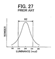
- Figs. 26 and 27 are graphs showing numeric data widely varied in chromaticity and luminance of LED devices.
- Fig. 26 is a graph of XYZ chromaticity coordinates showing variation in chromaticity of LED devices by 1 lot mass production. Each black point indicates the chromaticity of an LED device. The variation is in an upward zonal arrangement. Here, the dispersion of the black points in the width direction shown by the letter A means the variation of chromaticity of the blue LED, the dispersion in the longitudinal direction shown by the letter B means the variation of quantity and distribution of the phosphor particles in the encapsulating resin.
- An LED device having chromaticity which is largely deviated from a central value in Fig. 26 can not be used as a device for emitting white light. It is frequently desirable that the LED device has chromaticity in a central range shown by hatching where X and Y are in a range of 0. 33 ± 0.01.
- In the graph of Fig. 27, the horizontal axis shows luminance and the vertical axis shows the number of LED devices. The luminance variation is distributed in +30% to - 40% range from the center of the distribution. However, a desirable range R2 is about ± 20% as shown by arrows in Fig. 27.
- An object of the present invention is to provide a white light emitting device which may correct distributions of the chromaticity and luminance in a desired range.
- According to the present invention, there is provided a white light emitting device comprising a blue light emitting element, a cover member for covering the blue light emitting element, fluorescent material being mixed in the cover member for converting wavelength of light emitted from the blue light emitting element to adjust chromaticity of the light, and luminance reducing material being mixed in the cover member for adjusting the luminance of the light.
- The luminance reducing material is pigment or dye for reducing the luminance irrespective of the wavelength of the light emitting from the light emitting element.
- The cover member is formed with elastomer of silicon group in which the fluorescent material and the luminance reducing material are mixed.
- The present invention further provides a white light emitting device comprising a case body having a recess forming a reflection face, a blue light emitting element mounted on a bottom of the recess, a cover member including fluorescent material and covering a light emitting face of the case body, fluorescent material being mixed in the cover member for converting wavelength of light emitted from the blue light emitting element to adjust chromaticity of the light, and luminance reducing material being mixed in the cover member for adjusting the luminance of the light.
- In an aspect of the invention, the white light emitting device further comprises a cover member holding portion formed in the recess of the case body, the cover member being mounted on the cover member holding portion.
- The recess is formed into a cup shape having an inclination surface open to a light emitting direction, the cover member has an inclined peripheral wall so as to be engaged with the inclination surface.
- In another aspect of the invention, the white light emitting device further comprises a shoulder formed in the recess of the case body for holding the cover member.
- The blue light emitting element is mounted on the bottom of the recess by face down bonding.
- Theblue light emitting element is mounted on a substrate by face down bonding to form a light emitting unit, and the substrate is mounted on the bottom of the recess.
- The blue light emitting element is an LED of InGaN group.
- The fluorescent material is a fluorescent material of YAG group.
- The luminance reducing material is a pigment of black.
- The present invention also provides a white light emitting device comprising, acasebodyhavingarecess forming a reflection face, a blue light emitting element mounted on a bottom of the recess, a cover member including fluorescent material and covering a light emitting face of the case body, the case body comprising a pair of metal cores which are opposed to each other interposing an insulation member, the surface of each of the metal cores being coated with a metal plating having high reflectance, fluorescent material for converting wavelength of light emitted from the blue light emitting element to adjust chromaticity of the light, and luminance reducing material for adjusting the luminance of the light being mixed in the cover member.
- The metal case is made of a magnesium alloy, the surface of the metal core is coated with silver plating.
- The cover member has arms, the arms are engaged with grooves formed in the case body.
- A projection is formed on the arm of the cover member, the projection is engaged with an engaging hole formed in the groove of the case body.
- The cover member is provided by separating from a cover member assembly comprising a plurality of cover members which are connected by arms.
- These and other objects and features of the present invention will become more apparent from the following detailed description with reference to the accompanying drawings.
-
- Fig. 1 is a perspective view of a white light emitting device according to a first embodiment of the present invention;
- Fig. 2 is a perspective view of the white light emitting device in which a cover member in Fig. 1 is removed;
- Fig. 3 is a sectional view of the white light emitting device taken along a line III - III of Fig. 1;
- Fig. 4 is a perspective view of a light emitting unit;
- Fig. 5 is a sectional view showing a white light emitting device according to a second embodiment of the present invention;
- Fig. 6 is a perspective view showing a white light emitting device according to a third embodiment of the present invention;
- Fig. 7 is a perspective view of the white light emitting device as viewed from a reverse side thereof;
- Fig. 8 is a sectional view taken along a line VIII - VIII of Fig. 6;
- Fig. 9 is a flowchart showing the steps for manufacturing the third embodiment;
- Figs. 10, 11, 12, 13a and 13b are perspective views for explaining a method for manufacturing a light emitting element unit assembly;
- Fig. 14 is a perspective view of a metal core assembly;
- Figs. 15, 16, 17 and 18 are perspective views for explaining a method for manufacturing a light emitting device;
- Fig. 19 is a perspective view showing a method for combining a light emitting element unit and a cover member;
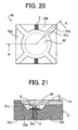
- Fig. 20 is a plan view showing a white light emitting device according to a fourth embodiment of the present invention;
- Fig. 21 is a sectional view of the device taken along a line A - A of Fig. 20;
- Figs. 22a to 22c are perspective views for explaining a method of manufacturing a white light emitting device of a fourth embodiment;
- Fig. 23 is a plan view of a white light emitting device according to a fifth embodiment of the present invention;
- Fig. 24 is a sectional view of the device taken along a line B - B of Fig. 23;
- Fig. 25 is a sectional view of a conventional LED device disclosed in US Patent 6,069,440; and
- Figs. 26 and 27 are graphs showing dispersion in chromaticity and luminance of LED devices.
-
- Fig. 1 is a perspective view of a white light emitting device according to a first embodiment of the present invention, Fig. 2 is a perspective view of the white light emitting device in which a cover member in Fig. 1 is removed, Fig. 3 is a sectional view of the white light emitting device taken along a line III - III of Fig. 1, and Fig. 4 is a perspective view of a light emitting element unit.
- Referring to Figs. 1 to 3, a white light emitting
LED device 10 comprises acubic case 1 made of moldable metal having a high heat conductivity such as Mg group and formed by injection molding, and having arecess 1c of an inverted truncated cone and having an inclined insidewall 1k. Thecase 1c comprises a pair of first and secondhalf metal cores insulation layer 2 which is made of resin and charged in aslit 1g. The inside wall of therecess 1c and anupper surface 1a of thecase 1c are processed into a light reflection surface by silver plating. - Referring to Fig. 4, a light emitting
element unit 5 comprises ablue LED 6 of InGaN group, asubstrate 7 made of ceramics and havingupper electrodes lower electrodes lower electrodes lower electrodes holes 7e, thereby forming a pair of wiring patterns. A pair ofbumps 6a (Fig. 3) are secured to a pair of electrodes (not shown) on the underside of theLED 6. Theblue LED 6 as a light emitting element is mounted on theupper electrodes bumps 6a by face down bonding. The underside of theLED 6 is encapsulated by aresin 8 to protect thebumps 6a. Further, theLED 6 is encapsulated by aresin 9. The light emittingelement unit 5 is mounted on the bottom of therecess 1c by soldering thelower electrodes metal cores - A
cover member 11 made of transparent resin such as elastomer of silicon group has an outside shape so as to engage with theinclined wall 1k of therecess 1c. If required, thecover member 11 is secured to therecess 1c by caulking or an adhesive . In thecover member 11,YAGphosphorparticles 12 and a luminance reducingmaterial particles 13 such as pigment and dye particles 7f are mixed. Thephosphor particle 12 and thepigment particle 13 are selected so that the chromaticity and luminance of the light emitted from theLED 6 are corrected to desired values. - As the phosphor particle is selected from fluorescent materials of YAG group where the ratio of Ga to Gd is variously changed.
- As the luminance reducing material, pigments of black group in which graphite and carbon or red, green and blue pigments are mixed are used.
- In operation, when the current is applied to the
metal cores blue LED 6 via theelectrodes LED 6 is excited to emit blue light. When a part of the blue light impinges upon thephosphor particle 12, the blue light is absorbed in thephosphor particle 12 and the particle emits yellow light. When the yellow light and the blue light which does not impinge upon the phosphor particle are mixed, white light produces. Further, the chromaticity and luminance of the white light are corrected to desired chromaticity and luminance by thephosphor particles 12 andpigment particles 13. - Since the
case 1 is made of a metal having a high heat conductivity, the case is superior in heat radiation. Therefore, the LED device can effectively be used for a light emitting device in which the case temperature rises highly because of a large current. - There is provided the
cover member 11 in which thephosphor particles 12 and theluminance reducing particles 13 are mixed. A whitelight emitting device 1 satisfies both of the chromaticity and luminance in a desired range, thereby reducing the variation in characteristics. Since the luminance reducing member is used, initial luminance can be set to a large value, so that the luminance is adjusted by reducing the luminance. Therefore, luminance can be adjusted in a wide range. - Since the
cover member 11 is made of the elastomer of silicon group, thephosphor particles 12 and theluminance reducing particles 13 are uniformly distributed in the cover member without depositing and biasing. Therefore, the LED device emits light uniform in chromaticity and luminance. - Fig. 5 is a sectional view showing a white light emitting device according to a second embodiment of the present invention. The white
light emitting device 20 has thecase 1 same as that of the first embodiment. Acover plate 14 made of glass or transparent solid plastic such as acrylic resin and silicon is secured to theupper surface 1a to press thecover member 11 against the inside wall of therecess 1c. Other parts are identified by the same reference numerals as Fig. 3. - Since the
cover member 11 is held by thecover plate 14, it is not necessary to adhere thecover member 11 to the wall of therecess 1k. - Fig. 6 is a perspective view showing a white light emitting device according to a third embodiment of the present invention. Fig. 7 is a perspective view of the white light emitting device as viewed from a reverse side thereof, Fig. 8 is a sectional view taken along a line VIII - VIII of Fig. 6.
- Referring to Figs. 6 and 7, the white
light emitting device 30 comprises acase 21 having a cubic shape. Thecase 21 comprises a pair ofmetal cores resin 24 of heat resistivity. The combiningresin 24 is mounted on astep 21f of thecase 21 to form an upper shape of the case, charged in aslit 21g between themetal cores grooves metal cores - The undersides of the
metal cores electrodes recess 21c is formed in themetal cores recess 21c and the surfaces of themetal cores shoulder 21e is formed in an upper portion of therecess 21c, and acover member 32 is mounted on the shoulder. Other parts are the same as the first embodiment and identified by the same reference numerals as the first embodiment. - Fig. 9 is a flowchart showing the steps for manufacturing the third embodiment, and Figs . 10 - 18 are perspective views showing the steps, whereby a plurality of light emitting element devices are manufactured at the same time.
- At a step S1, a substrate assembly for a light emitting element unit is manufactured.
- Fig. 10 is a perspective view of a
substrate assembly 107. - The
substrate assembly 107 is divided into nineareas 24 for nine LED devices by dicinglines electrodes 107b are secured. - In each area, a pair of through-
holes 107c are formed to electrically connect the upper andlower electrodes 107b. - At a step S2, the
blue LED 6 is mounted on theupper electrodes 107b through bumps (not shown) as shown in Fig. 11. Further, at a step S3, the underside of theLED 6 is encapsulated by theresin 8 and encapsulatingresin 9 to form a light emittingelement unit assembly 105 as shown in Fig. 12. - Next, at a step S4, the light emitting
element unit assembly 105 is cut off along the dicinglines element unit 5 from theassembly 105 as shown in Fig. 13b. - The chromaticity and luminance of each of the produced lighting element units are measured. The measured units are classified into ranks dependent on the result of the measurement.
- Next, at a step S5, a metal core assembly is manufactured. As shown in Fig. 14, a
metal core assembly 123 is formed by injection molding and divided into nineareas 30 for nineunits 5 by dicinglines cylindrical portion 123b having recess 21c is formed in eacharea 30 at a central portion. Threeslits 123g are formed in parallel to thelines 32 except aperipheral frame 123a. - Further, three
grooves 123c are formed. - At a step S6, a resin is charged in a recess within the
peripheral frame 123a, slits 123g andgrooves 123c to form aresin layer 104 as shown in Fig. 15. Thus, acase assembly 121 is produced. - Next, at a step S7, light emitting
element units 5 belonging to the same class are mounted onbottoms 21d ofrecesses 21c as shown in Fig. 16. - At a step S8,
cover members 32 belonging to the same rank are secured to the inside wall of therecesses 21c, respectively, to form a light emittingelement device assembly 130 as shown in Fig. 17. - At a step S9, the
assembly 130 is cut off along the dicinglines light emitting device 30 as shown in Fig. 18. - Finally, at a step S10, the test of the product is carried out.
- Fig. 19 is a perspective view showing a method for combining a blue light emitting element unit and a cover member.
- A method for combining the blue
light emitting element 6 and thecover member 32 is described hereinafter with reference to Fig. 19. - The
blue LED 6 in theunit 5 is measured about the chromaticity and the luminance by an LED tester, and measured LEDs are classified into classes, for example classes a, b, c, in accordance with the measured characteristics. - On the other hand, the
cover members 32 are also classified into classes A, B and C so that the combinations a and A, b and B, c and C perform to emit desirable white lights. The combined sets are mounted in thecase 21. Thus, whitelight emitting devices 30 are produced. - In accordance with the third embodiment, since the
shoulder 21e is formed in therecess 21c, thecover member 32 can easily be set in the recess. On the inside wall of therecess 21c, thevertical wall 21m is formed, and theside wall 32a of thecover member 32 is accordingly vertical. Therefore, when the cover member is set in therecess 21c, it is not necessary to judge the distinction of both sides of the cover member. - Fig. 20 is a plan view showing a white light emitting device according to a fourth embodiment of the present invention, Fig. 21 is a sectional view of the device taken along a line A - A of Fig. 21. The white
light emitting device 40 comprises acase 31 comprising a pair ofmetal cores slit 33c between themetal cores device 40 is characterized in that fourgrooves 31a are formed in the upper surfaces of themetal cores recess 21c . On the other hand, fourarms 42a are radially extending from acover member 42, corresponding to thegrooves 31a . Thearms 42a are engaged in thegrooves 31a and secured thereto. - Since the method for manufacturing the white light emitting device of the fourth embodiment is substantially same as that of the third embodiment, only different method is described hereinafter.
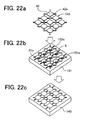
- Figs. 22a ∼ 22c are perspective views showing steps for manufacturing a light emitting device assembly. Referring to Fig. 22a, nine
cover members 42 are assembled by connectingarms 42a of eachcover member 42, thereby forming acover member assembly 142. - On the other hand, in a
case assembly 131 as shown in Fig. 22b, ninerecesses 21c,grooves 131a and slits 133c are formed. The light emittingelement unit 5 is mounted in eachrecess 21c. - As shown in Fig. 22c, the
cover member assembly 142 is mounted on thecase assembly 131. Thus a light emittingdevice assembly 140 is formed. - In accordance with the fourth embodiment, a plurality of
cover members 42 having the same characteristics are assembled. Therefore, light emitting devices of same characteristics can be produced. Further, constructing steps are reduced. - Fig. 23 is a plan view of a white light emitting device according to a fifth embodiment of the present invention, Fig. 24 is a sectional view of the device taken along a line B - B of Fig. 23 . The white
light emitting device 50 comprises acase 41 comprising a pair ofmetal cores slit 43c between themetal cores light emitting device 50, fourgrooves 41a are formed in the upper surfaces of themetal cores recess 21c. In one of thegrooves 41a, an engaginghole 41j is formed in the bottom of the groove. On the other hand, fourarms 51a are radially extending from acover member 51 and aprojection 51c is formed on the underside of thearm 51a corresponding to thehole 41j of thegroove 41a. Thearms 51a are engaged in thegrooves 41a and theprojection 51c is engaged withhole 41j and secured thereto. - In accordance with the fifth embodiment, the
cover member 51 is strongly fixed to thecase 41 by the engagement of theprojection 51c with thehole 41j. - In accordance with the present invention, there is provided the cover member in which the phosphor particles and the luminance reducing particles are mixed. Therefore the white light emitting device produces white light which satisfies both of the chromaticity and luminance in a desired range by selecting the amount of the phosphor and luminance reducing particles, thereby reducing the dispersion in characteristics.
- Since the luminance reducing member is used, initial luminance can be set to a large value, so that the luminance is adjusted by reducing the luminance. Therefore, luminance can be adjusted in a wide range.
- Since the cover member is made of the elastomer of silicon group, the phosphor particles and the luminance reducing particles are uniformly distributed in the cover member without depositing and biasing. Therefore, the LED device emits light uniform in chromaticity and luminance.
- While the invention has been described in conjunction with preferred specific embodiment thereof, it will be understood that this description is intended to illustrate and not limit the scope of the invention, which is defined by the following claims.
Claims (17)
- A white light emitting device comprising:a blue light emitting element;a cover member for covering the blue light emitting element;fluorescent material for converting wavelength of light emitted from the blue light emitting element to adjust chromaticity of the light being mixed in the cover member, and luminance reducing material for adjusting the luminance of the light being mixed in the cover member.
- The white light emitting device according to claim 1 wherein the luminance reducing material is pigment or dye for reducing the luminance irrespective of the wavelength of the light emitting from the light emitting element.
- The white light emitting device according to claim 1 wherein the cover member is formed from elastomer of silicon group in which the fluorescent material and the luminance reducing material are mixed.
- A white light emitting device comprising:a case body having a recess forming a reflection face;a blue light emitting element mounted on a bottom of the recess;a cover member including fluorescent material and covering a light emitting face of the case body;fluorescent material for converting wavelength of light emitted from the blue light emitting element to adjust chromaticity of the light, and luminance reducing material for adjusting the luminance of the light being mixed in the cover member.
- The white light emitting device according to claim 4 further comprising a cover member holding portion formed in the recess of the case body, the cover member being mounted on the cover member holding portion.
- The white light emitting device according to claim 4 wherein the recess is formed into a cup shape having an inclination surface open to a light emitting direction, the cover member has an inclined peripheral wall so as to be engaged with the inclination surface of the recess.
- The white light emitting device according to claim 5 further comprising a shoulder formed in the recess of the case body for holding the cover member.
- The white light emitting device according to claim 4 wherein the blue light emitting element is mounted on the bottom of the recess by face down bonding.
- The white light emitting device according to claim 4 wherein the blue light emitting element is mounted on a substrate by face down bonding to form a light emitting unit, and the substrate is mounted on the bottom of the recess.
- The white light emitting device according to claim 1 wherein the blue light emitting element is an LED of InGaN group.
- The white light emitting device according to claim 1 wherein the fluorescent material is a fluorescent material of YAG group.
- The white light emitting device according to claim 1 wherein the luminance reducing material is a pigment of black.
- A white light emitting device comprising:a case body having a recess forming a reflection face,a blue light emitting element mounted on a bottom of the recess,a cover member including fluorescent material and covering a light emitting face of the case body,the case body comprising a pair of metal cores which are opposed to each other interposing an insulation member, the surface of each of the metal cores being coated with a metal plating having high reflectance,fluorescent material for converting wavelength of light emitted from the blue light emitting element to adjust chromaticity of the light being mixed in the cover member, and luminance reducing material for adjusting the luminance of the light being mixed in the cover member.
- The white light emitting device according to claim 13 wherein the metal core is made of a magnesium alloy, the surface of the metal core is coated with silver plating.
- The white light emitting device according to claim 4 wherein the cover member has arms, the arms are engaged with grooves formed in the case body.
- The white light emitting device according to claim 15 wherein a projection is formed on the arm of the cover member, the projection is engaged with an engaging hole formed in the groove of the case body.
- The white light emitting device according to claim 15 wherein the cover member is provided by separating from a cover member assembly comprising a plurality of cover members which are connected by arms.
Applications Claiming Priority (2)
| Application Number | Priority Date | Filing Date | Title |
|---|---|---|---|
| JP2002294326 | 2002-10-07 | ||
| JP2002294326A JP4280050B2 (en) | 2002-10-07 | 2002-10-07 | White light emitting device |
Publications (2)
| Publication Number | Publication Date |
|---|---|
| EP1408559A2 true EP1408559A2 (en) | 2004-04-14 |
| EP1408559A3 EP1408559A3 (en) | 2006-07-05 |
Family
ID=32025495
Family Applications (1)
| Application Number | Title | Priority Date | Filing Date |
|---|---|---|---|
| EP03256244A Withdrawn EP1408559A3 (en) | 2002-10-07 | 2003-10-03 | White light emitting device |
Country Status (6)
| Country | Link |
|---|---|
| US (1) | US7180240B2 (en) |
| EP (1) | EP1408559A3 (en) |
| JP (1) | JP4280050B2 (en) |
| KR (1) | KR100655252B1 (en) |
| CN (1) | CN1310345C (en) |
| TW (1) | TWI236159B (en) |
Cited By (11)
| Publication number | Priority date | Publication date | Assignee | Title |
|---|---|---|---|---|
| WO2006005062A3 (en) * | 2004-06-30 | 2006-07-13 | Cree Inc | Chip-scale methods for packaging light emitting devices and chip-scale packaged light emitting devices |
| WO2007036206A1 (en) * | 2005-09-30 | 2007-04-05 | Osram Opto Semiconductors Gmbh | Optoelectronic component which emits electromagnetic radiation, and method for production of an optoelectronic component |
| GB2432967A (en) * | 2005-11-30 | 2007-06-06 | Unity Opto Technology Co Ltd | White light LED with fluorescent powder containing wavelength converting plate |
| EP1900040A1 (en) * | 2005-07-04 | 2008-03-19 | Seoul Semiconductor Co., Ltd | Light emitting diode and method of fabricating the same |
| EP1811581A3 (en) * | 2006-01-24 | 2010-01-20 | Shinko Electric Industries Co., Ltd. | Method of producing light emitting apparatus |
| EP2226860A3 (en) * | 2009-03-02 | 2010-09-22 | LG Innotek Co., Ltd. | Light emitting device |
| US7977686B2 (en) | 2005-06-30 | 2011-07-12 | Cree, Inc. | Chip-scale methods for packaging light emitting devices and chip-scale packaged light emitting devices |
| US8378366B2 (en) | 2007-03-30 | 2013-02-19 | Osram Opto Semiconductors Gmbh | Electromagnetic radiation emitting optoelectronic component and method for manufacturing an optoelectronic component |
| EP2323182A3 (en) * | 2009-11-17 | 2014-04-02 | Stanley Electric Co., Ltd. | Light emitting device and method for manufacturing the same |
| WO2015036887A1 (en) * | 2013-09-13 | 2015-03-19 | Koninklijke Philips N.V. | Frame based package for flip-chip led |
| US9537065B2 (en) | 2011-08-12 | 2017-01-03 | Sharp Kabushiki Kaisha | Light-emitting device with reflective resin |
Families Citing this family (67)
| Publication number | Priority date | Publication date | Assignee | Title |
|---|---|---|---|---|
| JP3910144B2 (en) | 2003-01-06 | 2007-04-25 | シャープ株式会社 | Semiconductor light emitting device and manufacturing method thereof |
| JP4788109B2 (en) * | 2003-10-28 | 2011-10-05 | パナソニック電工株式会社 | Semiconductor light emitting device and manufacturing method thereof |
| WO2005073621A1 (en) * | 2004-01-29 | 2005-08-11 | Matsushita Electric Industrial Co., Ltd. | Led illumination light source |
| TWI244226B (en) * | 2004-11-05 | 2005-11-21 | Chen Jen Shian | Manufacturing method of flip-chip light-emitting device |
| TWI241034B (en) | 2004-05-20 | 2005-10-01 | Lighthouse Technology Co Ltd | Light emitting diode package |
| JP4485856B2 (en) * | 2004-06-10 | 2010-06-23 | スタンレー電気株式会社 | LED lamp for high power |
| US20060006791A1 (en) * | 2004-07-06 | 2006-01-12 | Chia Chee W | Light emitting diode display that does not require epoxy encapsulation of the light emitting diode |
| JP2006049442A (en) | 2004-08-02 | 2006-02-16 | Sharp Corp | Semiconductor light emission device and its manufacturing method |
| US7256057B2 (en) * | 2004-09-11 | 2007-08-14 | 3M Innovative Properties Company | Methods for producing phosphor based light sources |
| TWI245437B (en) * | 2004-11-16 | 2005-12-11 | Lighthouse Technology Co Ltd | Package structure of a surface mount device light emitting diode |
| KR100867515B1 (en) * | 2004-12-06 | 2008-11-07 | 삼성전기주식회사 | Light emitting device package |
| KR100580753B1 (en) | 2004-12-17 | 2006-05-15 | 엘지이노텍 주식회사 | Light emitting device package |
| JP4591071B2 (en) * | 2004-12-20 | 2010-12-01 | 日亜化学工業株式会社 | Semiconductor device |
| US7777247B2 (en) * | 2005-01-14 | 2010-08-17 | Cree, Inc. | Semiconductor light emitting device mounting substrates including a conductive lead extending therein |
| US20070001182A1 (en) * | 2005-06-30 | 2007-01-04 | 3M Innovative Properties Company | Structured phosphor tape article |
| US7294861B2 (en) * | 2005-06-30 | 2007-11-13 | 3M Innovative Properties Company | Phosphor tape article |
| US20070007542A1 (en) * | 2005-07-07 | 2007-01-11 | Sumitomo Electric Industries,Ltd. | White-Light Emitting Device |
| JP2007027278A (en) * | 2005-07-13 | 2007-02-01 | Shinko Electric Ind Co Ltd | Semiconductor device and manufacturing method thereof |
| JP4640248B2 (en) * | 2005-07-25 | 2011-03-02 | 豊田合成株式会社 | Light source device |
| KR100807015B1 (en) * | 2005-08-16 | 2008-02-25 | 가부시끼가이샤 도시바 | Light emitting device |
| JP2007073575A (en) * | 2005-09-05 | 2007-03-22 | Matsushita Electric Ind Co Ltd | Semiconductor light emitting device |
| US8044412B2 (en) | 2006-01-20 | 2011-10-25 | Taiwan Semiconductor Manufacturing Company, Ltd | Package for a light emitting element |
| JP2007194525A (en) * | 2006-01-23 | 2007-08-02 | Matsushita Electric Ind Co Ltd | Semiconductor light emitting device |
| JP4996101B2 (en) * | 2006-02-02 | 2012-08-08 | 新光電気工業株式会社 | Semiconductor device and manufacturing method of semiconductor device |
| JP5956937B2 (en) * | 2006-02-03 | 2016-07-27 | 日立化成株式会社 | Method for manufacturing package substrate for mounting optical semiconductor element |
| JP4828248B2 (en) * | 2006-02-16 | 2011-11-30 | 新光電気工業株式会社 | Light emitting device and manufacturing method thereof |
| KR100746749B1 (en) * | 2006-03-15 | 2007-08-09 | (주)케이디티 | Photoluminescent diffusion sheet |
| US7683475B2 (en) * | 2006-03-31 | 2010-03-23 | Dicon Fiberoptics, Inc. | LED chip array module |
| JP2007288050A (en) * | 2006-04-19 | 2007-11-01 | Shinko Electric Ind Co Ltd | Semiconductor device, and method for manufacturing same |
| JP3914954B1 (en) | 2006-05-24 | 2007-05-16 | 株式会社エレメント電子 | Light emitting device and manufacturing method thereof |
| JP2007335462A (en) * | 2006-06-12 | 2007-12-27 | Stanley Electric Co Ltd | Semiconductor compound element, and its fabrication process |
| CN101467270B (en) * | 2006-06-14 | 2013-03-27 | 皇家飞利浦电子股份有限公司 | Lighting device |
| TWM303493U (en) * | 2006-07-21 | 2006-12-21 | Lighthouse Technology Co Ltd | Support rack structure and metal support rack of side light source SMD LED |
| WO2008013097A1 (en) * | 2006-07-25 | 2008-01-31 | Showa Denko K.K. | Light emitting apparatus, display apparatus and method for manufacturing light emitting apparatus |
| US7663152B2 (en) * | 2006-08-09 | 2010-02-16 | Philips Lumileds Lighting Company, Llc | Illumination device including wavelength converting element side holding heat sink |
| US7889421B2 (en) * | 2006-11-17 | 2011-02-15 | Rensselaer Polytechnic Institute | High-power white LEDs and manufacturing method thereof |
| US7800304B2 (en) * | 2007-01-12 | 2010-09-21 | Avago Technologies Ecbu Ip (Singapore) Pte. Ltd. | Multi-chip packaged LED light source |
| KR100869640B1 (en) * | 2007-04-20 | 2008-11-21 | (주)원반도체 | Light Emitting Diode |
| KR101623422B1 (en) * | 2007-06-27 | 2016-05-23 | 더 리전츠 오브 더 유니버시티 오브 캘리포니아 | Optical designs for high-efficacy white-light emitting diodes |
| KR200451231Y1 (en) | 2007-09-27 | 2010-12-03 | 지잉 퉁 텍. 메탈 코., 엘티디. | Thermal module |
| US8247831B2 (en) * | 2007-11-20 | 2012-08-21 | Koninklijke Philipe Electronics N.V. | Side emitting device with wavelength conversion |
| JP5217800B2 (en) | 2008-09-03 | 2013-06-19 | 日亜化学工業株式会社 | Light emitting device, resin package, resin molded body, and manufacturing method thereof |
| DE102008045653B4 (en) * | 2008-09-03 | 2020-03-26 | Osram Opto Semiconductors Gmbh | Optoelectronic component |
| JP5327601B2 (en) | 2008-12-12 | 2013-10-30 | 東芝ライテック株式会社 | Light emitting module and lighting device |
| JP5482378B2 (en) * | 2009-04-20 | 2014-05-07 | 日亜化学工業株式会社 | Light emitting device |
| CN102782892B (en) * | 2010-03-12 | 2015-07-01 | 夏普株式会社 | Light-emitting device manufacturing method, light-emitting device, lighting device, backlight, liquid-crystal panel, display device, display device manufacturing method, display device drive method and liquid-crystal display device |
| KR101121745B1 (en) | 2010-03-31 | 2012-03-22 | (주)포인트엔지니어링 | Optical Element Device and Fabricating Method Thereof |
| US8941135B2 (en) | 2010-07-15 | 2015-01-27 | Nitto Denko Corporation | Light emissive ceramic laminate and method of making same |
| JP5595185B2 (en) * | 2010-08-27 | 2014-09-24 | 三菱電機株式会社 | Light emitting device and lighting apparatus |
| TWI446590B (en) * | 2010-09-30 | 2014-07-21 | Everlight Electronics Co Ltd | Light emitting diode package structure and manufacturing method thereof |
| KR101212654B1 (en) * | 2011-05-20 | 2012-12-14 | (주)라이타이저코리아 | Package for light emitting diode and method for manufacturing thereof |
| JP2011171769A (en) * | 2011-06-06 | 2011-09-01 | Toshiba Corp | Packing member for led-package |
| TW201306323A (en) * | 2011-07-31 | 2013-02-01 | Walsin Lihwa Corp | Light emitting diode device |
| KR101878270B1 (en) * | 2011-09-15 | 2018-07-13 | 엘지이노텍 주식회사 | Lighting device comprising photoluminescent plate and photoluminescent tape |
| JP5848562B2 (en) * | 2011-09-21 | 2016-01-27 | シチズン電子株式会社 | Semiconductor light emitting device and manufacturing method thereof. |
| CN102569600B (en) * | 2011-11-11 | 2014-12-10 | 深圳市瑞丰光电子股份有限公司 | LED (light emitting diode) packaging structure and reflection cup thereof |
| CN102403422A (en) * | 2011-11-17 | 2012-04-04 | 深圳市天电光电科技有限公司 | Processing method of LED packaging structure and LED packaging structure |
| US9240524B2 (en) * | 2012-03-05 | 2016-01-19 | Seoul Viosys Co., Ltd. | Light-emitting device and method of manufacturing the same |
| JP5153950B1 (en) * | 2012-04-18 | 2013-02-27 | E&E Japan株式会社 | Light emitting diode |
| CN111509112B (en) * | 2013-07-08 | 2024-04-02 | 亮锐控股有限公司 | Wavelength-converted semiconductor light emitting device |
| JP2015164234A (en) * | 2015-06-17 | 2015-09-10 | シチズン電子株式会社 | LED light-emitting device and manufacturing method thereof |
| JP6632834B2 (en) | 2015-08-24 | 2020-01-22 | スタンレー電気株式会社 | Light emitting device |
| JP6928424B2 (en) * | 2016-02-24 | 2021-09-01 | 日亜化学工業株式会社 | Fluorescent material and light emitting device |
| KR101902371B1 (en) | 2017-03-02 | 2018-09-28 | 주식회사 이츠웰 | Wavelength Selectable LED Package and LED Package Array with thereof |
| DE102017117425A1 (en) * | 2017-08-01 | 2019-02-07 | Osram Opto Semiconductors Gmbh | Method for producing an optoelectronic component |
| JP2019046989A (en) | 2017-09-04 | 2019-03-22 | スタンレー電気株式会社 | Semiconductor light emitting device and method of manufacturing the same |
| JP6675032B1 (en) * | 2019-07-08 | 2020-04-01 | 御田 護 | Semiconductor light emitting device |
Citations (7)
| Publication number | Priority date | Publication date | Assignee | Title |
|---|---|---|---|---|
| US6184544B1 (en) * | 1998-01-29 | 2001-02-06 | Rohm Co., Ltd. | Semiconductor light emitting device with light reflective current diffusion layer |
| EP1081771A2 (en) * | 1999-09-03 | 2001-03-07 | Hewlett-Packard Company | Light emitting device |
| US6319425B1 (en) * | 1997-07-07 | 2001-11-20 | Asahi Rubber Inc. | Transparent coating member for light-emitting diodes and a fluorescent color light source |
| EP1174931A2 (en) * | 2000-07-21 | 2002-01-23 | Nichia Corporation | Light emitting device, display apparatus with an array of light emitting devices, and display apparatus method of manufacture |
| EP1187226A1 (en) * | 2000-09-01 | 2002-03-13 | Citizen Electronics Co., Ltd. | Surface-mount type light emitting diode and method of manufacturing same |
| US20020139990A1 (en) * | 2001-03-28 | 2002-10-03 | Yoshinobu Suehiro | Light emitting diode and manufacturing method thereof |
| US20030102481A1 (en) * | 2001-11-26 | 2003-06-05 | Citizen Electronics Co., Ltd. | Light emitting diode device |
Family Cites Families (15)
| Publication number | Priority date | Publication date | Assignee | Title |
|---|---|---|---|---|
| DE29724848U1 (en) | 1996-06-26 | 2004-09-30 | Osram Opto Semiconductors Gmbh | Light-emitting semiconductor component with luminescence conversion element |
| JP3109472B2 (en) | 1997-09-26 | 2000-11-13 | 松下電器産業株式会社 | Light emitting diode |
| KR100345283B1 (en) | 1998-05-15 | 2002-10-25 | 테스텍 주식회사 | Contact led, manufacturing method thereof and contact input device using the same |
| US5959316A (en) * | 1998-09-01 | 1999-09-28 | Hewlett-Packard Company | Multiple encapsulation of phosphor-LED devices |
| JP2002043625A (en) | 2000-07-19 | 2002-02-08 | Koha Co Ltd | Led |
| JP2002050797A (en) * | 2000-07-31 | 2002-02-15 | Toshiba Corp | Semiconductor excitation phosphor light-emitting device and manufacturing method therefor |
| JP3900848B2 (en) | 2001-03-23 | 2007-04-04 | シチズン電子株式会社 | Light emitting diode |
| JP3891115B2 (en) * | 2001-04-17 | 2007-03-14 | 日亜化学工業株式会社 | Light emitting device |
| JP4114331B2 (en) * | 2001-06-15 | 2008-07-09 | 豊田合成株式会社 | Light emitting device |
| JP2003158301A (en) * | 2001-11-22 | 2003-05-30 | Citizen Electronics Co Ltd | Light emitting diode |
| JP2003163378A (en) * | 2001-11-26 | 2003-06-06 | Citizen Electronics Co Ltd | Surface mount light emitting diode and its manufacturing method |
| US20030141563A1 (en) * | 2002-01-28 | 2003-07-31 | Bily Wang | Light emitting diode package with fluorescent cover |
| US6917057B2 (en) * | 2002-12-31 | 2005-07-12 | Gelcore Llc | Layered phosphor coatings for LED devices |
| US6936857B2 (en) * | 2003-02-18 | 2005-08-30 | Gelcore, Llc | White light LED device |
| US6828590B2 (en) * | 2003-05-07 | 2004-12-07 | Bear Hsiung | Light emitting diode module device |
-
2002
- 2002-10-07 JP JP2002294326A patent/JP4280050B2/en not_active Expired - Fee Related
-
2003
- 2003-10-03 EP EP03256244A patent/EP1408559A3/en not_active Withdrawn
- 2003-10-06 TW TW092127665A patent/TWI236159B/en not_active IP Right Cessation
- 2003-10-07 US US10/679,490 patent/US7180240B2/en active Active
- 2003-10-07 KR KR1020030069507A patent/KR100655252B1/en not_active IP Right Cessation
- 2003-10-08 CN CNB2003101015379A patent/CN1310345C/en not_active Expired - Fee Related
Patent Citations (7)
| Publication number | Priority date | Publication date | Assignee | Title |
|---|---|---|---|---|
| US6319425B1 (en) * | 1997-07-07 | 2001-11-20 | Asahi Rubber Inc. | Transparent coating member for light-emitting diodes and a fluorescent color light source |
| US6184544B1 (en) * | 1998-01-29 | 2001-02-06 | Rohm Co., Ltd. | Semiconductor light emitting device with light reflective current diffusion layer |
| EP1081771A2 (en) * | 1999-09-03 | 2001-03-07 | Hewlett-Packard Company | Light emitting device |
| EP1174931A2 (en) * | 2000-07-21 | 2002-01-23 | Nichia Corporation | Light emitting device, display apparatus with an array of light emitting devices, and display apparatus method of manufacture |
| EP1187226A1 (en) * | 2000-09-01 | 2002-03-13 | Citizen Electronics Co., Ltd. | Surface-mount type light emitting diode and method of manufacturing same |
| US20020139990A1 (en) * | 2001-03-28 | 2002-10-03 | Yoshinobu Suehiro | Light emitting diode and manufacturing method thereof |
| US20030102481A1 (en) * | 2001-11-26 | 2003-06-05 | Citizen Electronics Co., Ltd. | Light emitting diode device |
Cited By (20)
| Publication number | Priority date | Publication date | Assignee | Title |
|---|---|---|---|---|
| US7329905B2 (en) | 2004-06-30 | 2008-02-12 | Cree, Inc. | Chip-scale methods for packaging light emitting devices and chip-scale packaged light emitting devices |
| WO2006005062A3 (en) * | 2004-06-30 | 2006-07-13 | Cree Inc | Chip-scale methods for packaging light emitting devices and chip-scale packaged light emitting devices |
| US7977686B2 (en) | 2005-06-30 | 2011-07-12 | Cree, Inc. | Chip-scale methods for packaging light emitting devices and chip-scale packaged light emitting devices |
| US8809892B2 (en) | 2005-07-04 | 2014-08-19 | Seoul Semiconductor Co., Ltd. | Light emitting diode and method of fabricating the same |
| EP1900040A4 (en) * | 2005-07-04 | 2011-01-19 | Seoul Semiconductor Co Ltd | Light emitting diode and method of fabricating the same |
| EP1900040A1 (en) * | 2005-07-04 | 2008-03-19 | Seoul Semiconductor Co., Ltd | Light emitting diode and method of fabricating the same |
| US8058662B2 (en) | 2005-07-04 | 2011-11-15 | Seoul Semiconductor Co., Ltd. | Light emitting diode and method of fabricating the same |
| US8476655B2 (en) | 2005-09-30 | 2013-07-02 | Osram Opto Semiconductors Gmbh | Electromagnetic-radiation-emitting optoelectronic component and method for producing an optoelectronic component |
| WO2007036206A1 (en) * | 2005-09-30 | 2007-04-05 | Osram Opto Semiconductors Gmbh | Optoelectronic component which emits electromagnetic radiation, and method for production of an optoelectronic component |
| GB2432967A (en) * | 2005-11-30 | 2007-06-06 | Unity Opto Technology Co Ltd | White light LED with fluorescent powder containing wavelength converting plate |
| US7708613B2 (en) * | 2006-01-24 | 2010-05-04 | Shinko Electric Industries Co., Ltd. | Method of producing light emitting apparatus |
| EP1811581A3 (en) * | 2006-01-24 | 2010-01-20 | Shinko Electric Industries Co., Ltd. | Method of producing light emitting apparatus |
| US8378366B2 (en) | 2007-03-30 | 2013-02-19 | Osram Opto Semiconductors Gmbh | Electromagnetic radiation emitting optoelectronic component and method for manufacturing an optoelectronic component |
| EP2226860A3 (en) * | 2009-03-02 | 2010-09-22 | LG Innotek Co., Ltd. | Light emitting device |
| US8860052B2 (en) | 2009-03-02 | 2014-10-14 | Lg Innotek Co., Ltd. | Light emitting device |
| EP2323182A3 (en) * | 2009-11-17 | 2014-04-02 | Stanley Electric Co., Ltd. | Light emitting device and method for manufacturing the same |
| US8746932B2 (en) | 2009-11-17 | 2014-06-10 | Stanley Electric Co., Ltd. | Light emitting device and method for manufacturing the same |
| US9537065B2 (en) | 2011-08-12 | 2017-01-03 | Sharp Kabushiki Kaisha | Light-emitting device with reflective resin |
| WO2015036887A1 (en) * | 2013-09-13 | 2015-03-19 | Koninklijke Philips N.V. | Frame based package for flip-chip led |
| US9698323B2 (en) | 2013-09-13 | 2017-07-04 | Koninklijke Philips N.V. | Frame based package for flip-chip LED |
Also Published As
| Publication number | Publication date |
|---|---|
| KR20040031661A (en) | 2004-04-13 |
| JP2004128424A (en) | 2004-04-22 |
| CN1310345C (en) | 2007-04-11 |
| JP4280050B2 (en) | 2009-06-17 |
| KR100655252B1 (en) | 2006-12-08 |
| EP1408559A3 (en) | 2006-07-05 |
| US20040070338A1 (en) | 2004-04-15 |
| US7180240B2 (en) | 2007-02-20 |
| TW200414568A (en) | 2004-08-01 |
| CN1497747A (en) | 2004-05-19 |
| TWI236159B (en) | 2005-07-11 |
Similar Documents
| Publication | Publication Date | Title |
|---|---|---|
| EP1408559A2 (en) | White light emitting device | |
| US6858456B2 (en) | Method for manufacturing a light emitting device | |
| US11749776B2 (en) | Optoelectronic semiconductor component | |
| EP2400567B1 (en) | Phosphor selection for a Light-Emitting Device | |
| CN100570913C (en) | Manufacturing method for LED | |
| US7300326B2 (en) | LED device and method for manufacturing the same | |
| US7977684B2 (en) | Light emitting package having screen layer | |
| JP2004128424A5 (en) | ||
| US6774406B2 (en) | Light emitting diode device | |
| US10236420B2 (en) | Color tunable LED assembly | |
| JP2002252376A (en) | Surface-mounted type light-emitting diode and its manufacturing method | |
| KR20070012501A (en) | Light-emitting device and method for manufacturing same | |
| JP7179923B2 (en) | Light emitting device and toning device | |
| JP4822499B2 (en) | Chip type LED | |
| EP1557890A1 (en) | White-light LED and method for regulating the generated light color of the white-light LED |
Legal Events
| Date | Code | Title | Description |
|---|---|---|---|
| PUAI | Public reference made under article 153(3) epc to a published international application that has entered the european phase |
Free format text: ORIGINAL CODE: 0009012 |
|
| AK | Designated contracting states |
Kind code of ref document: A2 Designated state(s): AT BE BG CH CY CZ DE DK EE ES FI FR GB GR HU IE IT LI LU MC NL PT RO SE SI SK TR |
|
| AX | Request for extension of the european patent |
Extension state: AL LT LV MK |
|
| PUAL | Search report despatched |
Free format text: ORIGINAL CODE: 0009013 |
|
| AK | Designated contracting states |
Kind code of ref document: A3 Designated state(s): AT BE BG CH CY CZ DE DK EE ES FI FR GB GR HU IE IT LI LU MC NL PT RO SE SI SK TR |
|
| AX | Request for extension of the european patent |
Extension state: AL LT LV MK |
|
| AKX | Designation fees paid | ||
| REG | Reference to a national code |
Ref country code: DE Ref legal event code: 8566 |
|
| STAA | Information on the status of an ep patent application or granted ep patent |
Free format text: STATUS: THE APPLICATION IS DEEMED TO BE WITHDRAWN |
|
| 18D | Application deemed to be withdrawn |
Effective date: 20070106 |