EP1420509A1 - EMI filter for power supply - Google Patents
EMI filter for power supply Download PDFInfo
- Publication number
- EP1420509A1 EP1420509A1 EP03257154A EP03257154A EP1420509A1 EP 1420509 A1 EP1420509 A1 EP 1420509A1 EP 03257154 A EP03257154 A EP 03257154A EP 03257154 A EP03257154 A EP 03257154A EP 1420509 A1 EP1420509 A1 EP 1420509A1
- Authority
- EP
- European Patent Office
- Prior art keywords
- power supply
- circuit
- emi filter
- filter circuit
- capacitor
- Prior art date
- Legal status (The legal status is an assumption and is not a legal conclusion. Google has not performed a legal analysis and makes no representation as to the accuracy of the status listed.)
- Withdrawn
Links
Images


Classifications
-
- H—ELECTRICITY
- H02—GENERATION; CONVERSION OR DISTRIBUTION OF ELECTRIC POWER
- H02M—APPARATUS FOR CONVERSION BETWEEN AC AND AC, BETWEEN AC AND DC, OR BETWEEN DC AND DC, AND FOR USE WITH MAINS OR SIMILAR POWER SUPPLY SYSTEMS; CONVERSION OF DC OR AC INPUT POWER INTO SURGE OUTPUT POWER; CONTROL OR REGULATION THEREOF
- H02M1/00—Details of apparatus for conversion
- H02M1/44—Circuits or arrangements for compensating for electromagnetic interference in converters or inverters
-
- H—ELECTRICITY
- H02—GENERATION; CONVERSION OR DISTRIBUTION OF ELECTRIC POWER
- H02M—APPARATUS FOR CONVERSION BETWEEN AC AND AC, BETWEEN AC AND DC, OR BETWEEN DC AND DC, AND FOR USE WITH MAINS OR SIMILAR POWER SUPPLY SYSTEMS; CONVERSION OF DC OR AC INPUT POWER INTO SURGE OUTPUT POWER; CONTROL OR REGULATION THEREOF
- H02M1/00—Details of apparatus for conversion
- H02M1/12—Arrangements for reducing harmonics from ac input or output
- H02M1/126—Arrangements for reducing harmonics from ac input or output using passive filters
Landscapes
- Engineering & Computer Science (AREA)
- Power Engineering (AREA)
- Physics & Mathematics (AREA)
- Electromagnetism (AREA)
- Power Conversion In General (AREA)
- Rectifiers (AREA)
- Dc-Dc Converters (AREA)
- Filters And Equalizers (AREA)
Abstract
Description
- The present invention relates generally to power supplies and, more specifically, the present invention relates to a switched mode power supply with an input electromagnetic interference (EMI) filter circuit.
- Electronic devices use power to operate. Switched mode power supplies or adapters are widely used to power electronic products as well as charge batteries used to power mobile products such as for example wireless phones, palm top computers, toys, etc. Switched mode power supplies generate EMI, which must be filtered to allow the power supply to meet national and international standards stipulating acceptable levels of EMI. This requires that the switched mode power supply include components at the input of the power supply that filter EMI in order to meet these standards. Furthermore, an input fuse is required to meet national and international safety standards.
- Known power supply techniques employ input EMI filter circuits of varying, complexity. The simplest form of input EMI filter is known as a pi filter and is used in low-power power supplies to reduce power supply cost. The fuse is a separate component, which is typically either designed solely for use as a fuse or as a resistor specifically designed to meet national and international safety standards as a fusible component.
- A power supply input EMI filter circuit is disclosed. In one embodiment, a method of filtering EMT in a power supply includes rectifying an AC signal with a rectifier, smoothing the rectified signal with a bulk storage capacitor to provide a DC output as an input to a power conversion circuit and filtering the EMI generated by the power conversion circuit from reaching the AC source by using the bulk capacitor and one or more inductors in combination with the AC source capacitance as an EMI filter. In one embodiment the method also includes the use of one or more of the inductors as a fusing element to meet safety requirements. Additional features and benefits of the present invention will become apparent from the detailed description and figures set forth below.
- The present invention detailed illustrated by way of example and not limitation in the accompanying figures.
- Figure 1 is a schematic illustrating a power supply input circuit including a fuse and input EMI filter circuit;
- Figure 2 is a schematic illustrating one embodiment of a power supply with a simplified input EMI filter circuit and fuse in accordance with the teachings of the present invention;
- Figure 3 is a schematic illustrating another embodiment of a power supply with a simplified input EMI filter and fuse circuit in accordance with the teachings of the present invention ;
- Figure 4A provides an illustration of one embodiment of a full wave rectifier utilizing a diode bridge in accordance with the teachings of the present invention ;
- Figure 4B provides an illustration of one embodiment of a half wave rectifier utilizing a single diode on one of the rails in accordance with the teachings of the present invention ;
- Figure 4C provides an illustration of one embodiment of a half wave rectifier utilizing a single diode on each of the rails in accordance with the teachings of the present invention;
- Figure 4D provides an illustration of one embodiment of a half wave rectifier utilizing a plurality of diodes on at least one of the rails in accordance with the teachings of the present invention;
- Figure 5 is a schematic illustrating yet another embodiment of a power supply with a simplified input EMI filter and fuse circuit in accordance with the teachings of the present invention; and
- Figure 6 is a schematic illustrating still another embodiment of a power supply with a simplified input EMI filter and fuse circuit in accordance with the teachings of the present invention.
-
- A technique to reduce the cost of input EMI filter circuitry in switched mode power supplies is disclosed. In the following description, numerous specific details are set forth in order to provide a thorough understanding of the present invention. It will be apparent, however, to one having ordinary skill in the art that the specific detail need not be employed to practice the present invention. In other instances, well-known materials or methods have not been described in detail in order to avoid obscuring the present invention.
- In one embodiment, the present invention provides a simplified input EMI circuit, which therefore reduces the cost and complexity of input EMI filter circuitry and the fuse function.
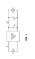
- To illustrate, Figure 1 shows a schematic of a power supply input stage including a
fuse 101, arectifier circuit 100 and EMI filtercircuitry including capacitors inductor 105. The input EMI filter circuitry is coupled in a coagulation that is known as a pi filter, which can be appreciated to one skilled in the art. As can be appreciated by one skilled in the art, therectifier circuit 100 can be either a well-known full or half wave rectifier circuit. If a full wave rectifier circuit is used, the rectification bridge ofrectifier circuit 100 can be constructed using either discrete diodes or a single component bridge rectifier. If a half wave rectifier circuit is used, therectifier circuit 100 can be constructed using a single diode or multiple diodes coupled in series. The latter construction is used in certain embodiments to reduce EMI and/or to increase the amount of input voltage surges thatrectifier circuit 100 can withstand, as will be appreciated to one skilled in the art. - The circuitry shown in Figure 1 has an
AC source 102 at the input and provides a rectified and smoothed or filtered DC output voltage atDC output 106. Such a configuration is typical of low power AC to DC power supply circuits such as those employed in low power (<10 Watts output) adapters and chargers for consumer electronics items and the like. As well as forming part of the pi filter,capacitors AC source 102 when the voltage across theAC source 102 is greater than the DC voltage acrosscapacitors AC source 102 throughcapacitors capacitors DC output 106 as required for efficient operation of a power conversion circuit that is to be coupled to receive the DC output voltage atDC output 106. - The
fuse 101 shown in Figure 1, which is coupled betweenAC source 102 andrectifier circuit 100 is a fusible resistor. In order for a resistor to fulfill the international standards required of a fuse component, the resistor is normally of a wore wound construction and covered in a flame retardant or heatshrink material that prevents pieces of the resistor being scattered when thefuse 101 is blown during a fault condition. The position of thefuse 101 is also important to ensure compliance of the power supply with international safety standards. - To comply with international safety standards, the
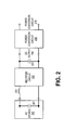
fuse 101 must be positioned such that it becomes an open circuit in the event of an abnormally high current being drawn fromAC source 102 due to a fault on any component in therectifier circuit 100, EMI filter consisting ofcomponents DC output 106. Figure 1 therefore shows the most obvious position forfuse 101 to ensure that it limits an abnormal current in the case of a fault in any component coming afterfuse 101. - Figure 2 shows a schematic illustrating one embodiment of a power supply input stage utilized in a power supply in accordance with the teachings of the present invention. In the illustrated embodiment, an AC signal from an
AC source 102 is rectified by rectifier circuit 200 and is then smoothed atDC output 106 bycapacitor 203. The circuit shown is a simplification of that shown in Figure 1 through the elimination of thefuse 101 and also one of thebulk storage capacitors inductor 202, which also forms part of an EMI filter as described later. As can be appreciated to one skilled in the art, typical input inductor components used in power supplies, such as for example below 10 Watts output, are typically constructed of a fine wire wound on a ferrite core. As such the construction is similar to thefusible resistor 101 described above. As such, by the correct choice of wire gauge (diameter),inductor 202 can be designed to become an open circuit under specific: conditions of abnormal current flow such as those due to a fault in one of the power supply components. In one embodiment, the position ofinductor 202, in common with thefuse 101 in Figure 1, is on theAC source 102 side of the rectifier circuit 200 to ensure circuit protection under any of the abnormal current conditions as described earlier. - The EMI filter configuration of the circuit in Figure 2 forms a pi filter with the single
bulk storage capacitor 203,inductor 202 andAC source capacitance 201 ofAC source 102. It is appreciated thatAC source capacitance 201 is a distributed source capacitance ofAC source 102, rather than a specific component. ThisAC source capacitance 201 is present in everyAC source 102 and is represented by an equivalent capacitance in the equipment used to make EMI measurements. This equipment is called a Line Impedance Stabilization Network (LISN), as will be familiar to one skilled in the art. The AC source or LISN capacitance can therefore be specifically used to form a pi filter with the simplified input circuitry of Figure 2 in accordance with the teachings of the present invention. Since EMI measurements are made under standardized conditions of input cable length and LISN circuitry, theAC source capacitance 201 is deterministic and provides repeatable measurements to ensure consistent EMI filter performance. - As shown in the depicted embodiment, rectifier circuit 200 is coupled between
inductor 202 andcapacitor 203. In one embodiment, the capacitance value ofcapacitor 203 is not necessarily equal to the value ofcapacitance 104 of Figure 1. In the depicted embodiment,capacitor 203 is a single capacitor and is adapted to provide the bulk storage function and is therefore usually a larger value of capacitance value than that ofcapacitor 104 to achieve the same average DC output voltage atDC output 106. However, despite typically being a larger capacitor, the elimination of one bulk storage capacitor typically provides a significant cost saving over the configuration in Figure 1 since the cost of each capacitor component is strongly influenced by the packaging itself, which is reduced using a single component. Furthermore, the elimination of one bulk storage capacitor reduces the cost of circuit assembly in production by reducing component count. In one embodiment,inductor 202 also does not necessarily have the same inductance value asinductor 105 and is chosen in each case to optimize the pi filter performance with theAC source capacitance 201 andbulk storage capacitor 203. In operation, the rectified and smoothed or filtered DC voltage atDC output 106 is received bypower conversion circuit 208, which generates an output voltage at powerconversion circuit output 210. In one embodiment,power conversion circuit 208 is a switched mode power converter and the EMI filter circuit of Figure 2 is employed to filter the EMI in accordance with the teaching of the present invention. - Figure 3 shows a schematic illustrating another embodiment of a power supply input stage employed in a power supply in accordance with the teachings of the present invention. The circuit shown.is again a simplification of that shown in Figure 1 through the elimination of the
fuse 101 and also one of thebulk storage capacitors inductor 302, which also forms part of the EMI filter. - In this configuration however, the
inductor 302 is placed on the output side of therectifier circuit 300. That is,rectifier circuit 300 is betweenAC source 102 andinductor 302. In one embodiment, this places a limitation on the type ofinput rectifier circuit 300 that can be used if the inductor is also required to perform the fuse function. This limitation arises since connection ofinductor 302 can only provide a fuse function in compliance with international safety standards described earlier if theinput rectifier circuit 300 is a half wave rectifier circuit. As can be appreciated by one skilled in the art, ifinput rectifier circuit 300 is a full wave bridge rectifier circuit, the short circuit failure of any one of the diodes in the rectification bridge will cause abnormally high current to be drawn fromAC source 102 without this current flowing throughinductor 302. In one embodiment, the circuit shown in Figure 3 is therefore limited to use wheninput rectifier circuit 300 is a half wave rectifier circuit if the inductor is also required to function as a fuse. - To illustrate, Figures 4A, 4B, 4C and 4D provide various example schematics of various embodiments of rectifiers that may be utilized in accordance with the teachings of the present invention. In particular, Figure 4A provides an illustration of one embodiment of a full wave rectifier utilizing a diode bridge: Figure 4B provides an illustration of one embodiment of a half wave rectifier utilizing a single diode on one of the rails. Figure 4C provides an illustration of one embodiment of a half wave rectifier utilizing a single diode on each of the rails. Figure 4D provides an illustration of one embodiment of a half wave rectifier utilizing a plurality of diodes on at least one of the rails. It is appreciated that other suitable variations of the schematics illustrated in Figures 4A, 4B, 4C and 4D may be utilized in accordance with the teachings of the present invention. Any one of the rectifier circuits shown could be used in the circuits of Figure 2, 3 or the circuits described below though their application is not limited to only those configurations shown in Figures 4A, 4B, 4C and 4D.
- As illustrated in Figures 4B, 4C and 4D, embodiments of the half wave rectifier circuit can be constructed using a single diode or multiple diodes coupled in series. When using multiple diodes, one or more diodes can be connected on either or both AC input rails. Using one or more diodes on both rails of the AC input reduces EMI by blocking the EMI generated by the power conversion circuit from being coupled to the AC source on both rails during times when the diodes are not conducting.
- As will be appreciated by one skilled in the art, in one embodiment, the configuration of Figure 3 can be used with
rectifier circuit 300 as a full wave rectifier circuit, such as for example the rectifier illustrated in Figure 4A, if a separate fuse component is used coupled in series with theAC source 102 on the input side ofrectifier circuit 300. In this embodiment,inductor 302 no longer provides the fuse function and the circuit complies with international safety standards. - Referring back to the embodiment of Figure 3, an AC signal is provided by
AC source 102 and is rectified byrectifier circuit 300 and smoothed bycapacitor 303 such that a rectified and smoothed or filtered DC signal is generated atDC output 106. The rectified and smoothed DC signal atDC output 106 is coupled to be received bypower conversion circuit 208 such that an output is generated atpower conversion output 210. In one embodiment,power conversion circuit 208 is a switched mode power converter. - The EMI filter function in the embodiment of Figure 3 is made up of
inductor 302,bulk storage capacitor 303 andAC source capacitance 201 ofAC source 102. In common with the embodiment of Figure 2, the AC source or LISN capacitance is used to form a pi filter with the simplified input circuitry of Figure 3. Other benefits of the simplified input circuitry of Figure 3 are common with those of the circuit illustrated in Figure 2 as described previously. - Figure 5 shows a schematic illustrating yet another embodiment of a power supply input stage of a power supply in accordance with the teachings of the present invention. In the embodiment depicted in Figure 5, the general configuration and functionality share similarities with the embodiment shown and described with respect to Figure 2. An AC signal is output by
AC source 102 and it is rectified byrectifier 500 and smoothed or filtered bycapacitor 503 to provide a DCsignal atDC output 106 atcapacitor 503.Power conversion circuit 208 receives the rectified and smoothed DC signal atDC output 106 such that an output is provided at powerconversion circuit output 210. - Two
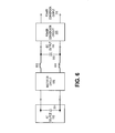
inductors input inductor 202 of the embodiment of Figure 2. In the illustrated embodiment,inductors AC source 102 andrectifier circuit 500. In one embodiment, the total inductance ofinductors inductor 202. For instance, in one embodiment, one of theinductors inductors inductors - Figure 6 shows a schematic illustrating still another embodiment of a power supply input stage used in a power supply in accordance with the teachings of the present invention. In Figure 6, the general configuration and functionality share similarities with the circuit shown in Figure 3. In the depicted embodiment, an AC signal is generated by
AC source 102 andrectifier circuit 600 rectifies the AC signal andcapacitor 603 smoothes the signal such that a rectified and smoothed or filtered DC signal is generated atDC output 106 atcapacitor 603. The rectified and smoothed DC signal atDC output 106 is received bypower conversion circuit 208 such that an output is generated at powerconversion circuit output 210. - The
input inductor 302 of embodiment Figure 3, however, has replaced by twoinductors rectifier circuit 600 is coupled betweenAC source 102 andinductors inductors inductor 302. For instance, in one embodiment, one of theinductors inductors inductors inductors - In one embodiment, the circuit embodiment of Figure 6 shares similar limitations as that of the circuit embodiment of Figure 3 in terms of the
input rectifier circuit 600. For instance, in one embodiment,rectifier circuit 600 must be a half wave rectifier circuit in order for the use of eitherinductor Rectifier circuit 600 can, however, be a full wave rectifier circuit if a separate fuse component is coupled between theAC source 102 and the input torectifier circuit 600. - In the foregoing detailed description, the present invention has been described with reference to specific exemplary embodiments thereof. It will, however, be evident that various modifications and changes may be made thereto without departing from the broader spirit and scope of the present invention. The present specification and figures are accordingly to be regarded as illustrative rather than restrictive.
Claims (46)
- A power supply input electromagnetic interference (EMI) filter circuit, comprising:an inductor to be coupled to an alternating current (AC) source having an AC source capacitance;a rectifier having an input coupled to the inductor, the inductor to be coupled between the AC source and the rectifier; anda capacitor coupled to an output of the rectifier such that an EMI pi filter is formed with the AC source capacitance, the inductor and the capacitor.
- A power supply EMI filter circuit of claim 1, wherein the capacitor is adapted to provide bulk storage for a direct current (DC) input of a power supply conversion circuit to be coupled to the capacitor.
- A power supply EMI filter circuit of claim 2, wherein the power conversion circuit is adapted to provide an output power of less than approximately ten Watts.
- A power supply EMI filter circuit of claim 2, wherein the capacitor that provides the bulk storage for the DC input of the power supply conversion circuit consists of a single capacitor.
- A power supply EMI filter circuit of claim 1, wherein the rectifier is a half wave rectifier circuit.
- A power supply EMI filter circuit of claim 5, wherein the half wave rectifier circuit includes a plurality of inputs and a corresponding plurality of outputs, wherein the half wave rectifier circuit comprises one or more diodes coupled between each of the inputs and the corresponding outputs of the half wave rectifier circuit.
- A power supply EMI filter circuit of claim 1, wherein the rectifier is a full wave rectifier circuit.
- A power supply EMI filter circuit of claim 1, wherein the inductor is adapted to function as a fuse to limit an abnormal amount of current flow.
- A power supply EMI filter circuit of claim 8, wherein the inductor is covered with a flame retardant material.
- A power supply EMI filter circuit of claim 8, wherein the inductor is covered with a heatshrink material.
- A power supply input electromagnetic interference (EMI) filter circuit, comprising:a rectifier having an input to be coupled to an alternating current (AC) source having an AC source capacitance;an inductor having a first terminal coupled to an output of the rectifier, the rectifier to be coupled between the AC source and the first terminal of the inductor; anda capacitor coupled to a second terminal of the inductor such that an EMI pi filter is formed with the AC source capacitance, the inductor and the capacitor.
- A power supply EMI filter circuit of claim 11, wherein the capacitor is adapted to provide bulk storage for a direct current (DC) input of a power supply conversion circuit to be coupled to the capacitor.
- A power supply EMI filter circuit of claim 12, wherein the power conversion circuit is adapted to provide an output power of less than approximately ten Watts.
- A power supply EMI filter circuit of claim 12, wherein the
capacitor that provides the bulk storage for the DC input of the power supply conversion circuit consists of a single capacitor. - A power supply EMI filter circuit of claim 11, wherein the rectifier is a half wave rectifier circuit.
- A power supply EMI filter circuit of claim 15, wherein the half wave rectifier circuit includes a plurality of inputs and a corresponding plurality of outputs, wherein the half wave rectifier circuit comprises one or more diodes coupled between each of the inputs and the corresponding outputs of the half wave rectifier circuit.
- A power supply EMI filter circuit of claim 11, wherein the rectifier is a full wave rectifier circuit.
- A power supply EMI filter circuit of claim 11, wherein the inductor is adapted to function as a fuse to limit an abnormal amount of current flow.
- A power supply EMI filter circuit of claim 18, wherei the inductor is covered with a flame retardant material.
- A power supply EMI filter circuit of claim 18, wherein the inductor is covered with a heatshrink material.
- A power supply input electromagnetic interference (EMI) filter circuit, comprising:a first inductor to be coupled to a first line of an alternating current (AC) source having an AC source capacitance;a second inductor to be coupled to a second line of the AC source;a rectifier having first and second inputs coupled to the first and second inductors, respectively, the first and second inductors to be coupled between the AC source and the rectifier, anda capacitor coupled to an output of the rectifier such that an EMI filter is formed with the AC source capacitance, the first and second inductors and the capacitor.
- A power supply EMI filter circuit of claim 21, wherein the capacitor is adapted to provide bulk storage for a direct current (DC) input of a power supply conversion circuit to be coupled to the capacitor.
- A power supply EMI filter circuit of clam 22, wherein the power conversion circuit is adapted to provide an output power of less than approximately ten Watts.
- A power supply EMI filter circuit of claim 22, wherein the capacitor that provides the bulk storage for the DC input of the power supply conversion circuit consists of a single capacitor.
- A power supply EMI filter circuit of claim 21, wherein the rectifier is a half wave rectifier circuit.
- A power supply EMI filter circuit of claim 25, wherein the half wave rectifier circuit includes a plurality of inputs and a corresponding plurality of outputs, wherein the half wave rectifier circuit comprises one or more diodes coupled between each of the inputs and the corresponding outputs of the half wave rectifier circuit.
- A power supply EMI filter circuit of claim 21, wherein the rectifier is a full wave rectifier circuit.
- A power supply EMI filter circuit of claim 21, wherein at least one or more of the first and second inductors are adapted to function as at least one or more fuses to limit an abnormal amount of current flow.
- A power supply EMI filter circuit of claim 28, wherein the at least one or more of the first and second inductors that are adapted to function as the at least one or more fuses to limit the abnormal amount of current flow are covered with a flame retardant material.
- A power supply EMI filter circuit of claim 28, wherein the at least one or more of the first and second inductors that are adapted to function as the at least one or more fuses to limit the abnormal amount of current flow are covered with a heatshrink material.
- A power supply input electromagnetic interference (EMI) filter circuit, comprising:a rectifier having an input to be coupled to an alternating current (AC) source having an AC source capacitance;a first inductor having a first terminal coupled to a first output of the rectifier;a second inductor having a first terminal coupled to a second output of the rectifier, the rectifier to be coupled between the AC source and the first and second inductors; anda capacitor coupled between a second terminal of the first inductor and a second terminal of the second inductor such that an EMI filter is formed with the AC source capacitance, the first and second inductors and the capacitor.
- A power supply EMI filter circuit of claim 31, wherein the capacitor is adapted to provide bulk storage for a direct current (DC) input of a power supply conversion circuit to be coupled to the capacitor.
- A power supply EMI filter circuit of claim 32, wherein the power conversion circuit is adapted to provide an output power of less than approximately ten Watts.
- A power supply EMI filter circuit of claim 32, wherein the capacitor that provides the bulk storage for the DC input of the power supply conversion circuit consists of a single capacitor.
- A power supply EMI filter circuit o claim 31, wherein the rectifier is a half wave rectifier circuit.
- A power supply EMI filter circuit of claim 35, wherein the half wave rectifier circuit includes a plurality of inputs and a corresponding plurality of outputs, wherein the half wave rectifier circuit comprises one or more diodes coupled between each of the inputs and the corresponding outputs of the half wave rectifier circuit.
- A power supply EMI filter circuit of claim 31, wherein the rectifier is a full wave rectifier circuit.
- A power supply EMI filter circuit of claim 31, wherein the inductor is adapted to function as a fuse to limit an abnormal amount of current flow.
- A power supply EMI filter circuit of claim 38, wherein the inductor is covered with a flame retardant material.
- A power supply EMI filter circuit of claim 38, wherein the inductor is covered with a heatshrink material.
- A method, comprising:rectifying an AC signal from an AC source;filtering the rectified AC signal with a bulk storage capacitor to. provide a DC signal to an input of a power conversion circuit; andfiltering the electromagnetic interference (EMI) generated by the power converter circuit with an EMI filter that includes an AC source capacitance of the AC source, one or more inductors and the bulk storage capacitor.
- A method of claim 41, wherein rectifying the AC signal comprises full wave rectifying the AC signal with a full wave rectifier.
- A method of claim 41, wherein rectifying the AC signal from the AC source comprises half wave rectifying the AC signal.
- A method of claim 41, further comprising limiting an abnormal amount of current from flowing with at least one of said one or more inductors that are included in the EMI filter.
- A method of claim 44, further comprising covering the at least one of said one or more inductors with a flame retardant material.
- A method of claim 44, further comprising covering the at least one of said one or more indicators with a heatshrink material.
Applications Claiming Priority (2)
| Application Number | Priority Date | Filing Date | Title |
|---|---|---|---|
| US10/299,175 US6813168B2 (en) | 2002-11-18 | 2002-11-18 | Method and apparatus for providing input EMI filtering in power supplies |
| US299175 | 2002-11-18 |
Publications (1)
| Publication Number | Publication Date |
|---|---|
| EP1420509A1 true EP1420509A1 (en) | 2004-05-19 |
Family
ID=32176224
Family Applications (1)
| Application Number | Title | Priority Date | Filing Date |
|---|---|---|---|
| EP03257154A Withdrawn EP1420509A1 (en) | 2002-11-18 | 2003-11-12 | EMI filter for power supply |
Country Status (3)
| Country | Link |
|---|---|
| US (2) | US6813168B2 (en) |
| EP (1) | EP1420509A1 (en) |
| JP (1) | JP2004180497A (en) |
Cited By (3)
| Publication number | Priority date | Publication date | Assignee | Title |
|---|---|---|---|---|
| US6813168B2 (en) | 2002-11-18 | 2004-11-02 | Power Integrations, Inc. | Method and apparatus for providing input EMI filtering in power supplies |
| EP2104218B1 (en) * | 2008-03-20 | 2017-08-23 | LS Industrial Systems Co., Ltd | Converter with a plurality of indirect voltage link a.c. converter units |
| CN113078811A (en) * | 2021-04-16 | 2021-07-06 | 中科汇安科技成都有限公司 | Command car communication equipment low electromagnetic radiation power supply unit |
Families Citing this family (59)
| Publication number | Priority date | Publication date | Assignee | Title |
|---|---|---|---|---|
| US7166968B2 (en) * | 1995-06-26 | 2007-01-23 | Jlj, Inc. | DC series connected light string with diode array shunt |
| EP1676356A1 (en) * | 2003-10-14 | 2006-07-05 | Koninklijke Philips Electronics N.V. | Power converter |
| US8253394B2 (en) | 2004-02-17 | 2012-08-28 | Hewlett-Packard Development Company, L.P. | Snubber circuit |
| US20050162870A1 (en) * | 2004-01-23 | 2005-07-28 | Hirst B. M. | Power converter |
| US7336904B2 (en) * | 2004-11-29 | 2008-02-26 | Finisar Corporation | Electro-magnetic interference reduction filter for an optical transceiver |
| US11881814B2 (en) | 2005-12-05 | 2024-01-23 | Solaredge Technologies Ltd. | Testing of a photovoltaic panel |
| US10693415B2 (en) | 2007-12-05 | 2020-06-23 | Solaredge Technologies Ltd. | Testing of a photovoltaic panel |
| JP4079178B2 (en) * | 2006-04-19 | 2008-04-23 | ダイキン工業株式会社 | Power converter, control method therefor, and air conditioner |
| TWI343586B (en) * | 2006-07-21 | 2011-06-11 | Delta Electronics Inc | Power source transforming device and transformer thereof |
| US8751053B2 (en) * | 2006-10-19 | 2014-06-10 | Tigo Energy, Inc. | Method and system to provide a distributed local energy production system with high-voltage DC bus |
| US8947194B2 (en) | 2009-05-26 | 2015-02-03 | Solaredge Technologies Ltd. | Theft detection and prevention in a power generation system |
| US11687112B2 (en) | 2006-12-06 | 2023-06-27 | Solaredge Technologies Ltd. | Distributed power harvesting systems using DC power sources |
| US11888387B2 (en) | 2006-12-06 | 2024-01-30 | Solaredge Technologies Ltd. | Safety mechanisms, wake up and shutdown methods in distributed power installations |
| US8473250B2 (en) | 2006-12-06 | 2013-06-25 | Solaredge, Ltd. | Monitoring of distributed power harvesting systems using DC power sources |
| US11728768B2 (en) | 2006-12-06 | 2023-08-15 | Solaredge Technologies Ltd. | Pairing of components in a direct current distributed power generation system |
| US9130401B2 (en) | 2006-12-06 | 2015-09-08 | Solaredge Technologies Ltd. | Distributed power harvesting systems using DC power sources |
| US11855231B2 (en) | 2006-12-06 | 2023-12-26 | Solaredge Technologies Ltd. | Distributed power harvesting systems using DC power sources |
| US8963369B2 (en) | 2007-12-04 | 2015-02-24 | Solaredge Technologies Ltd. | Distributed power harvesting systems using DC power sources |
| US8013472B2 (en) | 2006-12-06 | 2011-09-06 | Solaredge, Ltd. | Method for distributed power harvesting using DC power sources |
| US8618692B2 (en) | 2007-12-04 | 2013-12-31 | Solaredge Technologies Ltd. | Distributed power system using direct current power sources |
| US8319483B2 (en) | 2007-08-06 | 2012-11-27 | Solaredge Technologies Ltd. | Digital average input current control in power converter |
| US11296650B2 (en) | 2006-12-06 | 2022-04-05 | Solaredge Technologies Ltd. | System and method for protection during inverter shutdown in distributed power installations |
| US8384243B2 (en) | 2007-12-04 | 2013-02-26 | Solaredge Technologies Ltd. | Distributed power harvesting systems using DC power sources |
| US9112379B2 (en) | 2006-12-06 | 2015-08-18 | Solaredge Technologies Ltd. | Pairing of components in a direct current distributed power generation system |
| US11309832B2 (en) | 2006-12-06 | 2022-04-19 | Solaredge Technologies Ltd. | Distributed power harvesting systems using DC power sources |
| US8319471B2 (en) | 2006-12-06 | 2012-11-27 | Solaredge, Ltd. | Battery power delivery module |
| US11735910B2 (en) | 2006-12-06 | 2023-08-22 | Solaredge Technologies Ltd. | Distributed power system using direct current power sources |
| US8816535B2 (en) | 2007-10-10 | 2014-08-26 | Solaredge Technologies, Ltd. | System and method for protection during inverter shutdown in distributed power installations |
| US11264947B2 (en) | 2007-12-05 | 2022-03-01 | Solaredge Technologies Ltd. | Testing of a photovoltaic panel |
| WO2009072076A2 (en) | 2007-12-05 | 2009-06-11 | Solaredge Technologies Ltd. | Current sensing on a mosfet |
| WO2009118683A2 (en) | 2008-03-24 | 2009-10-01 | Solaredge Technolgies Ltd. | Zero voltage switching |
| EP3719949A1 (en) | 2008-05-05 | 2020-10-07 | Solaredge Technologies Ltd. | Direct current power combiner |
| US8098055B2 (en) * | 2008-08-01 | 2012-01-17 | Tigo Energy, Inc. | Step-up converter systems and methods |
| GB2485527B (en) | 2010-11-09 | 2012-12-19 | Solaredge Technologies Ltd | Arc detection and prevention in a power generation system |
| US10673222B2 (en) | 2010-11-09 | 2020-06-02 | Solaredge Technologies Ltd. | Arc detection and prevention in a power generation system |
| US10673229B2 (en) | 2010-11-09 | 2020-06-02 | Solaredge Technologies Ltd. | Arc detection and prevention in a power generation system |
| US10230310B2 (en) | 2016-04-05 | 2019-03-12 | Solaredge Technologies Ltd | Safety switch for photovoltaic systems |
| GB2486408A (en) | 2010-12-09 | 2012-06-20 | Solaredge Technologies Ltd | Disconnection of a string carrying direct current |
| GB2483317B (en) | 2011-01-12 | 2012-08-22 | Solaredge Technologies Ltd | Serially connected inverters |
| KR101789830B1 (en) * | 2011-08-09 | 2017-10-25 | 엘지이노텍 주식회사 | A circuit of input and output stage of a driver ic configured to mitigate electromagnetic interference |
| US20130057229A1 (en) * | 2011-09-02 | 2013-03-07 | Intersil Americas Inc. | Power factor correction apparatus and method |
| GB2498791A (en) | 2012-01-30 | 2013-07-31 | Solaredge Technologies Ltd | Photovoltaic panel circuitry |
| US9853565B2 (en) | 2012-01-30 | 2017-12-26 | Solaredge Technologies Ltd. | Maximized power in a photovoltaic distributed power system |
| GB2498790A (en) | 2012-01-30 | 2013-07-31 | Solaredge Technologies Ltd | Maximising power in a photovoltaic distributed power system |
| GB2499991A (en) | 2012-03-05 | 2013-09-11 | Solaredge Technologies Ltd | DC link circuit for photovoltaic array |
| CN103427622B (en) * | 2012-05-18 | 2016-08-03 | 台达电子工业股份有限公司 | Improve method and the power conversion unit of performance of filter |
| US10115841B2 (en) | 2012-06-04 | 2018-10-30 | Solaredge Technologies Ltd. | Integrated photovoltaic panel circuitry |
| BR112014031992A2 (en) | 2012-06-27 | 2017-06-27 | Koninklijke Philips Nv | circuit for receiving an output signal from a transformer; and device |
| US9099926B2 (en) * | 2012-10-11 | 2015-08-04 | Hamilton Sundstrand Corporation | System and method for connecting the midpoint of a dual-DC bus to ground |
| US9548619B2 (en) | 2013-03-14 | 2017-01-17 | Solaredge Technologies Ltd. | Method and apparatus for storing and depleting energy |
| US9941813B2 (en) | 2013-03-14 | 2018-04-10 | Solaredge Technologies Ltd. | High frequency multi-level inverter |
| EP3506370B1 (en) | 2013-03-15 | 2023-12-20 | Solaredge Technologies Ltd. | Bypass mechanism |
| US9318974B2 (en) | 2014-03-26 | 2016-04-19 | Solaredge Technologies Ltd. | Multi-level inverter with flying capacitor topology |
| US11177663B2 (en) | 2016-04-05 | 2021-11-16 | Solaredge Technologies Ltd. | Chain of power devices |
| US11018623B2 (en) | 2016-04-05 | 2021-05-25 | Solaredge Technologies Ltd. | Safety switch for photovoltaic systems |
| CN107307723A (en) * | 2016-04-26 | 2017-11-03 | 广东美的生活电器制造有限公司 | Cooking machine circuit and cooking machine |
| CN111614094B (en) * | 2019-02-22 | 2023-08-18 | 欧姆龙株式会社 | Electromagnetic interference filter circuit |
| CN113114382B (en) * | 2020-01-13 | 2023-09-01 | 华为技术有限公司 | Power supply filtering device |
| US11901812B1 (en) * | 2023-10-23 | 2024-02-13 | Xiaobin YANG | Power converter system with high conversion efficiency |
Citations (4)
| Publication number | Priority date | Publication date | Assignee | Title |
|---|---|---|---|---|
| US5818705A (en) * | 1995-07-13 | 1998-10-06 | Compaq Computer Corporation | Portable computer having built-in AC adapter incorporating a space efficient electromagnetic interference filter |
| DE20119996U1 (en) * | 2001-12-10 | 2002-03-28 | Pi Internat Ltd | Multi-purpose input device |
| US6400584B1 (en) * | 2001-03-23 | 2002-06-04 | Koninklijke Philips Electronics N.V. | Two stage switching power supply for connecting an AC power source to a load |
| US20020114176A1 (en) * | 2001-02-16 | 2002-08-22 | Sanken Electric Co., Ltd. | Low-noise switching power supply |
Family Cites Families (12)
| Publication number | Priority date | Publication date | Assignee | Title |
|---|---|---|---|---|
| US3273044A (en) * | 1962-12-19 | 1966-09-13 | Bell Telephone Labor Inc | Transformer replacement system |
| US4222096A (en) * | 1978-12-05 | 1980-09-09 | Lutron Electronics Co., Inc. | D-C Power supply circuit with high power factor |
| US4263549A (en) * | 1979-10-12 | 1981-04-21 | Corcom, Inc. | Apparatus for determining differential mode and common mode noise |
| US5017878A (en) * | 1987-10-01 | 1991-05-21 | Nave Mark J | Measuring and limiting EMI with a differential mode rejection network |
| EP0325379B1 (en) * | 1988-01-14 | 1997-03-19 | Kabushiki Kaisha Toshiba | Value determining method for line filter and its components |
| US5661390A (en) * | 1995-06-23 | 1997-08-26 | Electric Power Research Institute, Inc. | Inverter-fed motor drive with EMI suppression |
| US5619404A (en) * | 1995-10-30 | 1997-04-08 | Zak; Alexander | Multi-channel single stage high power factor AC to DC converter |
| US6051936A (en) * | 1998-12-30 | 2000-04-18 | Philips Electronics North America Corporation | Electronic lamp ballast with power feedback through line inductor |
| US6184630B1 (en) * | 1999-02-08 | 2001-02-06 | Philips Electronics North America Corporation | Electronic lamp ballast with voltage source power feedback to AC-side |
| US6233161B1 (en) * | 2000-03-02 | 2001-05-15 | Power Integrations, Inc. | Switched mode power supply responsive to voltage across energy transfer element |
| DE10118285A1 (en) * | 2001-04-12 | 2002-11-07 | Philips Corp Intellectual Pty | Circuit for converting AC voltage to DC voltage |
| US6813168B2 (en) | 2002-11-18 | 2004-11-02 | Power Integrations, Inc. | Method and apparatus for providing input EMI filtering in power supplies |
-
2002
- 2002-11-18 US US10/299,175 patent/US6813168B2/en not_active Expired - Fee Related
-
2003
- 2003-11-12 EP EP03257154A patent/EP1420509A1/en not_active Withdrawn
- 2003-11-18 JP JP2003387762A patent/JP2004180497A/en active Pending
-
2004
- 2004-09-23 US US10/948,945 patent/US7609535B2/en not_active Expired - Fee Related
Patent Citations (4)
| Publication number | Priority date | Publication date | Assignee | Title |
|---|---|---|---|---|
| US5818705A (en) * | 1995-07-13 | 1998-10-06 | Compaq Computer Corporation | Portable computer having built-in AC adapter incorporating a space efficient electromagnetic interference filter |
| US20020114176A1 (en) * | 2001-02-16 | 2002-08-22 | Sanken Electric Co., Ltd. | Low-noise switching power supply |
| US6400584B1 (en) * | 2001-03-23 | 2002-06-04 | Koninklijke Philips Electronics N.V. | Two stage switching power supply for connecting an AC power source to a load |
| DE20119996U1 (en) * | 2001-12-10 | 2002-03-28 | Pi Internat Ltd | Multi-purpose input device |
Non-Patent Citations (3)
| Title |
|---|
| CAPONET M C ET AL: "EMI filters design for power electronics", PESC REC IEEE ANNUAL POWER ELECTRONICS SPECIALISTS CONFERENCE; PESC RECORD, vol. 4, 23 June 2002 (2002-06-23), Cairns, Australia, pages 2027 - 2032, XP010596047 * |
| QU S ET AL: "Mixed-mode EMI noise and its implications to filter design in offline switching power supplies", APPLIED POWER ELECTRONICS CONFERENCE AND EXPOSITION, 2000. APEC 2000. FIFTEENTH ANNUAL IEEE NEW ORLEANS, LA, USA 6-10 FEB. 2000, PISCATAWAY, NJ, USA,IEEE, US, 6 February 2000 (2000-02-06), pages 707 - 713, XP010371609, ISBN: 0-7803-5864-3 * |
| SHUO WANG ET AL: "Improving the performance of boost PFC EMI filters", APEC 2003. 18TH. ANNUAL IEEE APPLIED POWER ELECTRONICS CONFERENCE AND EXPOSITION. MIAMI BEACH, FL, FEB. 9 - 13, 2003, ANNUAL APPLIED POWER ELECTRONICS CONFERENCE, NEW YORK, NY: IEEE, US, vol. 1 OF 2. CONF. 18, 9 February 2003 (2003-02-09), pages 368 - 374, XP010631536, ISBN: 0-7803-7768-0 * |
Cited By (5)
| Publication number | Priority date | Publication date | Assignee | Title |
|---|---|---|---|---|
| US6813168B2 (en) | 2002-11-18 | 2004-11-02 | Power Integrations, Inc. | Method and apparatus for providing input EMI filtering in power supplies |
| US7609535B2 (en) | 2002-11-18 | 2009-10-27 | Power Integrations, Inc. | Method and apparatus for providing input EMI filtering in power supplies |
| EP2104218B1 (en) * | 2008-03-20 | 2017-08-23 | LS Industrial Systems Co., Ltd | Converter with a plurality of indirect voltage link a.c. converter units |
| CN113078811A (en) * | 2021-04-16 | 2021-07-06 | 中科汇安科技成都有限公司 | Command car communication equipment low electromagnetic radiation power supply unit |
| CN113078811B (en) * | 2021-04-16 | 2023-08-08 | 中科汇安科技成都有限公司 | Low electromagnetic radiation power supply device for command vehicle communication equipment |
Also Published As
| Publication number | Publication date |
|---|---|
| US20050041442A1 (en) | 2005-02-24 |
| JP2004180497A (en) | 2004-06-24 |
| US20040095785A1 (en) | 2004-05-20 |
| US6813168B2 (en) | 2004-11-02 |
| US7609535B2 (en) | 2009-10-27 |
Similar Documents
| Publication | Publication Date | Title |
|---|---|---|
| US6813168B2 (en) | Method and apparatus for providing input EMI filtering in power supplies | |
| US7092262B2 (en) | System and method for pre-charging the DC bus of a utility connected power converter | |
| US8929107B2 (en) | Active surge protection in a power supply | |
| JP5099183B2 (en) | Start-up circuit | |
| US20160308399A1 (en) | Power transmission device and power reception device | |
| US20040027096A1 (en) | Auxiliary circuit for power factor corrector having self-power supplying and zero current detection mechanisms | |
| EP2672597A1 (en) | Voltage rectifier | |
| JP4240783B2 (en) | Non-contact power transmission device | |
| US20070109827A1 (en) | Ac to dc converter circuit | |
| US8503193B2 (en) | Open loop DC to DC converters with enable/disable circuits | |
| EP2596572A2 (en) | Power source circuit | |
| JP2012095446A (en) | Power supply unit and withstand voltage test method therefor | |
| JP2010004613A (en) | Power supply device | |
| JP3402031B2 (en) | DC power supply | |
| Sugawara et al. | 3rd-Gen. Critical Mode PFC Control IC “FA1 A00 Series” | |
| CN206259865U (en) | A kind of Switching Power Supply | |
| Collin et al. | Voltage disturbances and inrush current of DC power supplies | |
| CN217508597U (en) | 7.5W PSR constant power supply | |
| Cresswell et al. | The analysis of the occurrence of high in-rush currents in DC power supplies | |
| CN215344382U (en) | Multi-output flyback switching power supply circuit and air conditioner | |
| CN210867185U (en) | Winding surge suppression circuit and instrument | |
| JP6828839B2 (en) | Switching power supply | |
| CN220342045U (en) | Voltage drop prevention device and system | |
| CN216356479U (en) | Power supply unit and supervisory equipment | |
| US20030102947A1 (en) | Multipurpose input device |
Legal Events
| Date | Code | Title | Description |
|---|---|---|---|
| PUAI | Public reference made under article 153(3) epc to a published international application that has entered the european phase |
Free format text: ORIGINAL CODE: 0009012 |
|
| AK | Designated contracting states |
Kind code of ref document: A1 Designated state(s): AT BE BG CH CY CZ DE DK EE ES FI FR GB GR HU IE IT LI LU MC NL PT RO SE SI SK TR |
|
| AX | Request for extension of the european patent |
Extension state: AL LT LV MK |
|
| 17P | Request for examination filed |
Effective date: 20040719 |
|
| AKX | Designation fees paid |
Designated state(s): DE FR GB IT NL SE |
|
| 17Q | First examination report despatched |
Effective date: 20071005 |
|
| RAP3 | Party data changed (applicant data changed or rights of an application transferred) |
Owner name: POWER INTEGRATIONS, INC. |
|
| STAA | Information on the status of an ep patent application or granted ep patent |
Free format text: STATUS: THE APPLICATION IS DEEMED TO BE WITHDRAWN |
|
| 18D | Application deemed to be withdrawn |
Effective date: 20090814 |