EP1424745A1 - Multi-series connection type battery cell - Google Patents
Multi-series connection type battery cell Download PDFInfo
- Publication number
- EP1424745A1 EP1424745A1 EP02026408A EP02026408A EP1424745A1 EP 1424745 A1 EP1424745 A1 EP 1424745A1 EP 02026408 A EP02026408 A EP 02026408A EP 02026408 A EP02026408 A EP 02026408A EP 1424745 A1 EP1424745 A1 EP 1424745A1
- Authority
- EP
- European Patent Office
- Prior art keywords
- battery cell
- circuit
- pack
- cell pack
- battery cells
- Prior art date
- Legal status (The legal status is an assumption and is not a legal conclusion. Google has not performed a legal analysis and makes no representation as to the accuracy of the status listed.)
- Granted
Links
Images

Classifications
-
- H—ELECTRICITY
- H01—ELECTRIC ELEMENTS
- H01M—PROCESSES OR MEANS, e.g. BATTERIES, FOR THE DIRECT CONVERSION OF CHEMICAL ENERGY INTO ELECTRICAL ENERGY
- H01M10/00—Secondary cells; Manufacture thereof
- H01M10/42—Methods or arrangements for servicing or maintenance of secondary cells or secondary half-cells
- H01M10/4207—Methods or arrangements for servicing or maintenance of secondary cells or secondary half-cells for several batteries or cells simultaneously or sequentially
-
- H—ELECTRICITY
- H01—ELECTRIC ELEMENTS
- H01M—PROCESSES OR MEANS, e.g. BATTERIES, FOR THE DIRECT CONVERSION OF CHEMICAL ENERGY INTO ELECTRICAL ENERGY
- H01M10/00—Secondary cells; Manufacture thereof
- H01M10/42—Methods or arrangements for servicing or maintenance of secondary cells or secondary half-cells
- H01M10/425—Structural combination with electronic components, e.g. electronic circuits integrated to the outside of the casing
- H01M10/4257—Smart batteries, e.g. electronic circuits inside the housing of the cells or batteries
-
- Y—GENERAL TAGGING OF NEW TECHNOLOGICAL DEVELOPMENTS; GENERAL TAGGING OF CROSS-SECTIONAL TECHNOLOGIES SPANNING OVER SEVERAL SECTIONS OF THE IPC; TECHNICAL SUBJECTS COVERED BY FORMER USPC CROSS-REFERENCE ART COLLECTIONS [XRACs] AND DIGESTS
- Y02—TECHNOLOGIES OR APPLICATIONS FOR MITIGATION OR ADAPTATION AGAINST CLIMATE CHANGE
- Y02E—REDUCTION OF GREENHOUSE GAS [GHG] EMISSIONS, RELATED TO ENERGY GENERATION, TRANSMISSION OR DISTRIBUTION
- Y02E60/00—Enabling technologies; Technologies with a potential or indirect contribution to GHG emissions mitigation
- Y02E60/10—Energy storage using batteries
Definitions
- the present invention relates to a multi-series connection type battery cell pack that comprises a plurality of series-connected battery cells, a charge/discharge control switch connected between said plurality of battery cells and an output terminal for performing charge/discharge control, a plurality of protective circuits for detecting at least the voltage of each battery cell, and a control circuit for communication with a computing circuit for performing computation of pack detection signals including each detection signal from said plurality of protective circuits and external equipments, thereby performing management and control of signals in the pack including said detection signals.
- the present invention is also directed to a charger making use of a battery cell pack function to charge a battery cell pack comprising therein a detection circuit for detecting at least the voltages and charging currents of said plurality of battery cells and a control circuit that has a function of communicating with external equipment and converting said detection signals to digital data for management and control purposes.
- a battery cell pack comprising therein a plurality of series-connected rechargeable battery cells, e.g., lithium ion battery cells.
- a series connected type battery cell pack comprising four battery cells at most suffices.
- a multi-series connection type battery cell pack comprising at least 7 battery cells is needed because the voltage of the four-battery cell pack is unacceptably low.
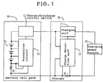
- Fig. 1 is a diagram showing a prior art battery cell pack and how to perform charge control with a charger.
- Reference numeral 10 is a battery cell pack, 11 cells, 12 a charge/discharge control switch, 13 a protective circuit, 20 a charger, 21 a charging unit, 22 a charge detection unit, 23 a charging power source, and Ri and R1 current detection resistances.
- the battery cell pack 10 has usually therein the charge/discharge control switch 12 that is series-connected between input/output terminals, the current detection resistance Ri for detection of discharging currents, and the protective circuit 13 for detecting cell voltages and discharging currents, thereby protecting the battery cells against overcharging and over-discharging, as shown in Fig. 1.
- the charger 20 for charging the cells 11 connected to the battery cell pack 10 is provided with the current detection resistance R1 for detection of charging currents for the battery cell pack 10, the charge detection unit 22 for detection of the charging voltage and current of the battery cell pack 10, and the charging unit 21 for performing control of the charging voltage and current fed from the charging power source 23 to the battery cell pack 10 and control of when to stop charging on the basis of the charging voltage and current detected by the charging detection unit 22.
- the charge/discharge control switch 12 series-connected between the cells 11 and the input/output terminals and comprising a charge control FET and a discharge control FET
- the protective circuit 13 for controlling a control microcomputer for communicating with outside to manage and control the battery cell pack and detecting the voltages and currents of the cells to control the charge control FET and discharge control FET.
- the protective circuit only low-voltage or medium-voltage protective ICs compatible with battery cell packs comprising four cells at most are commercialized because the standard type set for conventional battery cell packs like the battery cell pack 10 is still made up of up to 4 series-connected cells.
- the low- or medium-voltage protective ICs In new applications where battery cell packs whose voltage is higher than ever before are needed, as is the case with power sources for the aforesaid electrically aided bicycles, the low- or medium-voltage protective ICs must be connected together in a "protective IC s " unit.
- a problem with the control microcomputer is that when signals from the respective low- or medium-voltage protective ICs are processed, some inconveniences are caused during computations or communications unless the processing levels are appropriate to the varying voltage references of the low- or medium-voltage protective ICs.
- a close understanding of the charging voltage and current of the battery cell pack is an important factor in consideration of charging accuracy as well as evaluation of to what degree the battery cell pack deteriorates.
- a high-precision A/D converter or the like must thus be used on a charging unit to detect charging currents, resulting in a complicated, large, expensive circuit.
- One object of the present invention is to enable level conversion processing to be easily performed when a plurality of detection, protective circuits are used while they are connected each other. Another object of the present invention is to make it possible to reduce self-consumption in a battery cell pack over a long period of time. Yet another object of the present invention is to make it possible to have through a charger a precise understanding of what degree each cell in a battery cell pack is charged to and to improve the charger in terms of ease of operation, size, and reliability.
- a multi-series connection type battery cell pack characterized by comprising a plurality of series-connected battery cells, a charge/discharge control switch connected between said plurality of battery cells and an output terminal to perform charge/discharge control, a plurality of protective circuits for dividing said plurality of battery cells into a plurality of blocks to detect at least the voltage of each battery cell, a computing circuit for computation of pack detection signals including detection signals of said plurality of protective circuits and a level conversion circuit for unifying voltages references of said detection signals between said plurality of protective circuits and said computing circuit, wherein said plurality of protective circuits are joined in parallel with said battery cells in a multistage fashion.
- the computing circuit is characterized by having a function capable of communicating with external equipment, wherein a charge/discharge control signal is sent out to the uppermost-stage protective circuit of said plurality of protective circuits on the basis of an order from said external equipment or computation of said pack detection signals, so that said uppermost-stage protective circuit controls said charge/discharge control switch, one of said plurality of protective circuits includes as detection signals a detection signal for charging/discharging currents which is detected by a voltage across a current detection resistance connected between said plurality of battery cells and said output terminal, and said pack detection signal includes a temperature detection signal detected by a temperature detection thermistor located in a pack.
- Another multi-series connection type battery cell pack of the present invention is characterized by comprising a plurality of series-connected battery cells, a charge/discharge control switch connected between said plurality of battery cells and an output terminal to perform charge/discharge control, a protective circuit for detecting at least the voltage of each of said plurality of battery cells and a control circuit for communicating with external equipment to manage and control signals in said pack, inclusive of detection signals, wherein said control circuit has a switching function of making a switching between a mode wherein current consumption in said pack minimizes and a normal operation mode.
- said protective circuit comprises a plurality of protective circuits for dividing said plurality of batteries into a plurality of blocks to detect at least the voltages of the respective battery cells and between said protective circuit and said control circuit there is positioned a level conversion circuit to unify the voltage references of detection signals, wherein said plurality of protective circuits are joined in parallel with said battery cells in a multistage manner.
- the present invention also provides a charger that makes use of a battery cell pack function of charging a battery cell pack comprising therein a plurality of series-connected battery cells, a detection circuit for detecting at least the voltages and charging currents of said plurality of battery cells and a control circuit having a communication function capable of communicating with external equipment and for managing and controlling detection signals, which comprises a charging unit for charging said battery cell pack from a charging power source and a charge control means for communicating with said control circuit in said battery cell pack to acquire and compute said detection signals thereby controlling said charging unit, wherein said detection signals acquired at said charge control means are digital data converted at said control circuit in said battery cell pack.
- Fig. 1 is illustrative of a conventional battery cell pack and how to control charging with a conventional charger.
- Fig. 2 is illustrative of one embodiment of the multi-series connection type battery cell pack according to the present invention.
- Fig. 3 is illustrative of one specific construction of the level conversion circuit in the multi-series connection type battery cell pack according to the present invention.
- Fig. 4 is illustrative of one embodiment of the charger making use of the battery cell pack function according to the present invention.
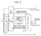
- FIG. 2 One embodiment of the multi-series connection type battery cell pack according to the present invention is shown in Fig. 2, wherein reference numeral 1 is a battery, 2 a charge/discharge control switch, 3-1 a detection circuit, 3-2 a detection circuit, 4 a level conversion circuit, and 5 a control microcomputer.
- reference numeral 1 is a battery
- 2 a charge/discharge control switch
- 3-1 a detection circuit
- 3-2 a detection circuit
- 4 a level conversion circuit
- 5 a control microcomputer.
- the battery 1 is an assembly of, for instance, seven battery cells that are series-connected to produce the desired voltage, and the charge/discharge control switch 2 is inserted in series between the battery 1 and an output terminal for performing charge/discharge control.
- the detection circuit 3-1 is connected in parallel with cells at the first to fourth stages of the battery 1 to detect the voltages of the cells
- the detection circuit 3-2 is a combined detective and protective means using a commercially available protective IC as an example, which means is connected in parallel with three cells at the fifth to seventh stages to detect the voltages of the cells and perform the on-off operation of the charge/discharge control switch 2.
- the detection circuits 3-1 and 3-2 are placed under control and management of the control microcomputer 5, and serve to transfer the cell voltages and discharging currents as analog detection signals (Aout) on a request from the control microcomputer 5.
- Aout analog detection signals
- the "circuit”, “means” and “IC” are thought of as being conceptually equivalent to one another.
- the level conversion circuit 4 performs level conversion for unifying voltage references for detection data (Aout) from the detection circuit 3-1, which are transferred to the control microcomputer 5.
- the detection circuits 3-1 and 3-2 each comprising a low- or medium-voltage protective IC, are used for high-voltage protection while they are joined together as shown, it is preferable to perform level conversion processing at the level conversion circuit 4, because it is possible to unify the voltage references for the purpose of executing computation and communication regardless of control.
- the control microcomputer 5 is a computing means for communicating with external equipment via control signals and data, controlling the detection circuits 3-1 and 3-2 and level conversion circuit 4 through a digital control line, and collecting successively analog detection signals from the detection circuits 3-1 and 3-2, thereby computing pack detection signals inclusive of these detection signals.
- control microcomputer 5 On the basis of computation of control commands from external equipment and pack detection signals, the control microcomputer 5 sends an on-off control signal for the charge/discharge control switch 2 to the detection circuit 3-2. In response to this, the detection circuit 3-2 controls the on-off operation of the charge/discharge control switch 2.
- control microcomputer 5 manages as a single unit a plurality of circuits (device ICs) in the pack such as detection circuits 3-1 and 3-2 and level conversion circuit 4, so that when they are not used or not in operation, they can be switched over to an operation mode where current consumption minimizes. This in turn makes it possible to reduce current consumption to the necessary minimum level thereby preventing deep discharge while battery cell packs are not used or stocked by makers or stored by users as spares.
- the control microcomputer 5 sends on-off control signals for the charge/discharge control switch 2 to the detection circuit 3-2. In response to this, the detection circuit 3-2 controls the on-off operation of the charge/discharge control switch 2.
- detection circuits and devices when information about conventionally joined battery cells is detected by detection circuits and devices, detection circuits and devices corresponding to the detectable number of series-connected battery cells are connected and inserted together to convert to the pack voltage reference information about the devices, including detection signals for the voltages of the series-connected cells, so that such information can be batch processed by a processing device. It is thus possible to use as the processing device a microcomputer that can be built depending on users' specific conditions, and perform settings and controls specific to battery cells and pack products.
- the pack can be so stored intact over an extended period of time that deep discharge breakdowns (deterioration) during storage can be minimized.
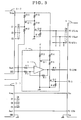
- FIG. 3 is illustrative of the specific construction of the multi-series connection type battery cell pack according to the present invention.
- Reference numeral 4-1 is an operational amplifier
- Q1, Q2, Q3 and Q4 are control transistors
- R1 to R8 and R11 to R14 are resistances
- CN is a digital signal line.
- detection circuits 3-1 and 3-2 each comprise a similar protective IC as shown in Fig. 2 (for instance, IC: M61040FP manufactured by Mitsubishi Electric Corporation).
- Vreg stands for a regulating power terminal
- D1, CK and CS are input terminals for digital control signals CN and CN'
- Aout is an output terminal for an analog detection signal.
- a control microcomputer 5 comprises a similar control IC as in the control microcomputer of Fig.
- Vcc represents a bias power terminal
- P0 2/Sclk, P0 1/Sout and P0 0/Sin indicate output terminals for digital control signals
- P3 1/AN and P3 2/AN mean input terminals for analog detection signals
- P0 6 stands for a control terminal for a level conversion circuit.
- a level conversion circuit 4 is made up of an operational amplifier 4-1 (e.g., IC: uPC1251G2 manufactured by NEC), control transistors Q1 and Q2 and resistances R1 to R8, and operates to unify voltage references (GND) of analog detection signals sent out of the output terminal Aout of the detection circuit 3-1 and analog detection signals sent out of the output terminal Aout of the detection circuit 3-2 to the control microcomputer 5.
- an operational amplifier 4-1 e.g., IC: uPC1251G2 manufactured by NEC
- control transistors Q1 and Q2 and resistances R1 to R8 operates to unify voltage references (GND) of analog detection signals sent out of the output terminal Aout of the detection circuit 3-1 and analog detection signals sent out of the output terminal Aout of the detection circuit 3-2 to the control microcomputer 5.
- the operational amplifier 4-1 operates to compute analog detection signals sent out of the output terminal Aout of the detection circuit 3-2 on a reference terminal (GND) voltage basis, and perform level conversion in such a way that analog detection signals entered in the input terminal P3 2/AN of the control computer 5 are on the same voltage reference (GND) level as analog detection signals entered in the input terminal P3 1/AN of the control microcomputer 5.
- GND reference terminal
- the control transistors Q1 and Q2 are to control the operation of the level conversion circuit 4.
- the on-off operation of the control transistor Q2 is controlled through the control microcomputer 5, so that the control transistor Q1 is put on or off.
- the level conversion circuit 4 is placed in operation only when required, so that during other periods the control transistor Q1 is held off to reduce useless energy consumption.
- the control microcomputer 5 sends the digital control signals CN out of its output terminals P0 2/Sclk, P0 1/Sout and P0 0/Sin to set specific information and operating conditions, so that the detection circuits 3-1 and 3-2 are controlled to selectively send detection signals and execute the on-off operation of the charge/discharge control switch, as already explained.
- the control transistor Q2 By performing on-off control of the control transistor Q2 in the level conversion circuit 4 by means of the output terminal P0 6, the on-off operation of the control transistor Q1 is controlled to control the operation of the level conversion circuit 4.
- the detection circuit 3-1 is on the lowermost stage; the digital control signals CN are entered directly in the input terminals D1, DK and CS, so that the cell voltages detected from the output terminal Aout on demand are sent out in the form of analog detection signals.
- the detection circuit 3-2 is joined to the upper stage of the detection signal 3-1; digital control signals CN' are entered in the input terminals D1, CK and CS via a signal conversion circuit made up of control transistors Q11-Q12 and resistances R11-R14, so that the cell voltages detected from the output terminal Aout on demand are likewise sent out in the form of analog detection signals.
- Fig. 4 is illustrative of one embodiment of the charger that makes use of the battery cell pack function according to the present invention.
- Reference numeral 7 stands for a charging unit, 8 a charge control unit, A a battery cell pack, B a charger, Ri a current detection resistance and Th a thermistor.
- the charger B comprises the charge control unit 8 that communicates with the battery cell pack A to acquire detection data such as the voltages, charging currents, temperatures, etc. of battery cells in the battery cell pack A, thereby computing the charging voltage that amounts to the sum of the voltages of the cells, judging what state the cells are charged in, and performing other predetermined computations, and the charging unit 7 that, on the basis of the results of computations at the charge control unit 8, performs control of charging voltage and current supplied from a charging power source to the battery cell pack A as well as of control of when charging is to be stopped.
- the charger B does not include circuits such as current detection resistance for direct detection of charging voltage and currents and an A/D converter.
- the charger B is designed to acquire data that are detected in the battery cell pack for the purpose of protecting overcharging, over-charging and overheating by means of communication, so that the data are processed to obtain information that is used for charge control.
- the battery cell pack A is a battery cell pack as explained with reference to Figs. 2 and 3.
- This battery cell pack comprises therein a charge/discharge control switch 2, detection circuits 3-1 and 3-2, a control microcomputer 5, etc.
- the detection circuit 3-1 is connected in parallel with cells at the first to fourth stages of a battery 1 to detect the voltages of the cells and to detect charge/discharge currents from a voltage across a current detection resistance Ri.
- the control microcomputer 5 communicates with external equipment via control signals and data to control the detection circuits 3-1 and 3-2 through a digital control line, so that analog detection signals are successively collected from the detection circuits 3-1 and 3-2, and pack detection signals including these detection signals and temperature detection signals are converted to digital detection signals for computing operation.
- the thermistor Th is located in the vicinity of the battery 1 to detect temperatures.
- the battery cell pack information about voltage, current, temperature, etc. is used to control the charge/discharge control switch for protection purposes. According to the present invention, however, these data are acquired from the charger side via communication, whereby conventional high-precision A/D converters, voltage/current detection circuits, etc. built in the charger can be dispensed with.
- individual detection data on the battery cell pack can be used as such; the degree of deterioration of the cells and variations in that degree can be so judged that charge control can be performed with higher precision than achieved so far by detection of charging voltage and current on the charger side. In short, depending on the degree of deterioration of individual cells and variations in that degree, which cannot be controlled on a conventional charger, charging voltage and current can be controlled to judge whether or not full-charge is achieved.
- the detection and protective circuits have been described with reference to a series-connected four-cell arrangement, it is appreciated that the present invention may be applied to any desired number of series-connected cells.
- the control microcomputer is designed just only to perform computation of cell voltages and charge/discharge currents detected from the respective detection circuits, but also to perform computation of temperatures detected by a thermistor located in the pack, etc.
- the on-off operation of the charge/discharge control switch is carried out by the upper-stage detection circuit on the basis of control signals from the control microcomputer.
- the present invention provides a multi-series connection type battery cell pack, characterized by comprising a plurality of series-connected battery cells, a charge/discharge control switch connected between said plurality of battery cells and an output terminal to perform charge/discharge control, a plurality of protective circuits for dividing said plurality of battery cells into a plurality of blocks to detect at least the voltage of each battery cell, a computing circuit for computation of pack detection signals including detection signals of said plurality of protective circuits and a level conversion circuit for unifying voltages references of said detection signals between said plurality of protective circuits and said computing circuit, wherein said plurality of protective circuits are joined in parallel with said battery cells in a multistage fashion.
- the present invention provides a multi-series connected type battery cell pack, comprising a plurality of series-connected battery cells, a charge/discharge control switch connected between said plurality of battery cells and an output terminal to perform charge/discharge control, a protective circuit for detecting at least the voltage of each of said plurality of battery cells and a control circuit for communicating with external equipment to manage and control signals in said pack, inclusive of detection signals, wherein said control circuit has a switching function of making a switching between a mode wherein current consumption in said pack minimizes and a normal operation mode. It is thus possible to switch the battery cell pack over to the minimum current consumption mode when it is not in use, so that the failure rate upon long-term storage can be held back.
- the aforesaid protective circuit comprises a plurality of protective circuits for dividing said plurality of batteries into a plurality of blocks to detect at least the voltages of the respective battery cells and between said protective circuit and said control circuit there is positioned a level conversion circuit to unify the voltage references of detection signals, wherein said plurality of protective circuits are joined in parallel with said battery cells in a multistage manner.
- the present invention also provides a charger that makes use of a battery cell pack function of charging a battery cell pack comprising therein a plurality of series-connected battery cells, a detection circuit for detecting at least the voltages and charging currents of said plurality of battery cells and a control circuit having a communication function capable of communicating with external equipment and for managing and controlling detection signals, which comprises a charging unit for charging said battery cell pack from a charging power source and a charge control means for communicating with said control circuit in said battery cell pack to acquire and compute said detection signals thereby controlling said charging unit. It is thus possible to dispense with circuits such as circuits for detection of charging voltages and currents and A/D converters, which have so far been built in a charger.
- the charger of the present invention it is only needed to have a minimum function as a dedicated charger, and so the circuit can be simplified and downsized with increased reliability.
- the circuit can be simplified and downsized with increased reliability.
- by processing information detected on the individual cells in the battery cell pack it is possible to have a more precise understanding of the charging state of the pack, and so achieve an inexpensive yet high-function charger capable of charging depending on the charging state.
Abstract
Description
- The present invention relates to a multi-series connection type battery cell pack that comprises a plurality of series-connected battery cells, a charge/discharge control switch connected between said plurality of battery cells and an output terminal for performing charge/discharge control, a plurality of protective circuits for detecting at least the voltage of each battery cell, and a control circuit for communication with a computing circuit for performing computation of pack detection signals including each detection signal from said plurality of protective circuits and external equipments, thereby performing management and control of signals in the pack including said detection signals. The present invention is also directed to a charger making use of a battery cell pack function to charge a battery cell pack comprising therein a detection circuit for detecting at least the voltages and charging currents of said plurality of battery cells and a control circuit that has a function of communicating with external equipment and converting said detection signals to digital data for management and control purposes.
- So far, portable electronic equipments such as cellular phones, notebook personal computers, players and digital cameras have been operated using as power sources a battery cell pack comprising therein a plurality of series-connected rechargeable battery cells, e.g., lithium ion battery cells. For these equipments that do not need any extremely high source voltages, a series connected type battery cell pack comprising four battery cells at most suffices. However, when such a type battery cell pack is intended for use as a power source for electrically aided bicycles that are now enjoying a growing popularity, for instance, a multi-series connection type battery cell pack comprising at least 7 battery cells is needed because the voltage of the four-battery cell pack is unacceptably low.
- Fig. 1 is a diagram showing a prior art battery cell pack and how to perform charge control with a charger.
Reference numeral 10 is a battery cell pack, 11 cells, 12 a charge/discharge control switch, 13 a protective circuit, 20 a charger, 21 a charging unit, 22 a charge detection unit, 23 a charging power source, and Ri and R1 current detection resistances. - The conventional battery cell pack, and how to perform charge control with a charger is now summarily explained. In addition to the cells 11, the
battery cell pack 10 has usually therein the charge/discharge control switch 12 that is series-connected between input/output terminals, the current detection resistance Ri for detection of discharging currents, and theprotective circuit 13 for detecting cell voltages and discharging currents, thereby protecting the battery cells against overcharging and over-discharging, as shown in Fig. 1. Thecharger 20 for charging the cells 11 connected to thebattery cell pack 10 is provided with the current detection resistance R1 for detection of charging currents for thebattery cell pack 10, thecharge detection unit 22 for detection of the charging voltage and current of thebattery cell pack 10, and thecharging unit 21 for performing control of the charging voltage and current fed from thecharging power source 23 to thebattery cell pack 10 and control of when to stop charging on the basis of the charging voltage and current detected by thecharging detection unit 22. - As explained above, in the
battery cell pack 10 there are provided the charge/discharge control switch 12 series-connected between the cells 11 and the input/output terminals and comprising a charge control FET and a discharge control FET, and theprotective circuit 13 for controlling a control microcomputer for communicating with outside to manage and control the battery cell pack and detecting the voltages and currents of the cells to control the charge control FET and discharge control FET. For this protective circuit, however, only low-voltage or medium-voltage protective ICs compatible with battery cell packs comprising four cells at most are commercialized because the standard type set for conventional battery cell packs like thebattery cell pack 10 is still made up of up to 4 series-connected cells. - In new applications where battery cell packs whose voltage is higher than ever before are needed, as is the case with power sources for the aforesaid electrically aided bicycles, the low- or medium-voltage protective ICs must be connected together in a "protective ICs" unit. On the other hand, a problem with the control microcomputer is that when signals from the respective low- or medium-voltage protective ICs are processed, some inconveniences are caused during computations or communications unless the processing levels are appropriate to the varying voltage references of the low- or medium-voltage protective ICs.
- In such applications where a plurality of low- or medium-voltage protective ICs are used, internal power consumptions increase. This in turn leads to another problem that pack storability becomes drastically worse or some packs are susceptible to over-discharging while they are let stand.
- For a charger for charging a battery cell pack, on the other hand, a close understanding of the charging voltage and current of the battery cell pack is an important factor in consideration of charging accuracy as well as evaluation of to what degree the battery cell pack deteriorates. For a conventional charger, a high-precision A/D converter or the like must thus be used on a charging unit to detect charging currents, resulting in a complicated, large, expensive circuit. Especially in the case of such a multi-series connection type as set forth above, it is important to have an understanding of the degree of deterioration of each cell in the battery cell pack; in the conventional charger, however, it is impossible to keep track of the degree of deterioration of each cell.
- One object of the present invention is to enable level conversion processing to be easily performed when a plurality of detection, protective circuits are used while they are connected each other. Another object of the present invention is to make it possible to reduce self-consumption in a battery cell pack over a long period of time. Yet another object of the present invention is to make it possible to have through a charger a precise understanding of what degree each cell in a battery cell pack is charged to and to improve the charger in terms of ease of operation, size, and reliability.
- According to the present invention, these objects are achievable by the provision of a multi-series connection type battery cell pack, characterized by comprising a plurality of series-connected battery cells, a charge/discharge control switch connected between said plurality of battery cells and an output terminal to perform charge/discharge control, a plurality of protective circuits for dividing said plurality of battery cells into a plurality of blocks to detect at least the voltage of each battery cell, a computing circuit for computation of pack detection signals including detection signals of said plurality of protective circuits and a level conversion circuit for unifying voltages references of said detection signals between said plurality of protective circuits and said computing circuit, wherein said plurality of protective circuits are joined in parallel with said battery cells in a multistage fashion.
- In one specific embodiment of this aspect of the present invention, the computing circuit is characterized by having a function capable of communicating with external equipment, wherein a charge/discharge control signal is sent out to the uppermost-stage protective circuit of said plurality of protective circuits on the basis of an order from said external equipment or computation of said pack detection signals, so that said uppermost-stage protective circuit controls said charge/discharge control switch, one of said plurality of protective circuits includes as detection signals a detection signal for charging/discharging currents which is detected by a voltage across a current detection resistance connected between said plurality of battery cells and said output terminal, and said pack detection signal includes a temperature detection signal detected by a temperature detection thermistor located in a pack.
- Another multi-series connection type battery cell pack of the present invention is characterized by comprising a plurality of series-connected battery cells, a charge/discharge control switch connected between said plurality of battery cells and an output terminal to perform charge/discharge control, a protective circuit for detecting at least the voltage of each of said plurality of battery cells and a control circuit for communicating with external equipment to manage and control signals in said pack, inclusive of detection signals, wherein said control circuit has a switching function of making a switching between a mode wherein current consumption in said pack minimizes and a normal operation mode.
- In one specific embodiment of this aspect of the present invention, said protective circuit comprises a plurality of protective circuits for dividing said plurality of batteries into a plurality of blocks to detect at least the voltages of the respective battery cells and between said protective circuit and said control circuit there is positioned a level conversion circuit to unify the voltage references of detection signals, wherein said plurality of protective circuits are joined in parallel with said battery cells in a multistage manner.
- The present invention also provides a charger that makes use of a battery cell pack function of charging a battery cell pack comprising therein a plurality of series-connected battery cells, a detection circuit for detecting at least the voltages and charging currents of said plurality of battery cells and a control circuit having a communication function capable of communicating with external equipment and for managing and controlling detection signals, which comprises a charging unit for charging said battery cell pack from a charging power source and a charge control means for communicating with said control circuit in said battery cell pack to acquire and compute said detection signals thereby controlling said charging unit, wherein said detection signals acquired at said charge control means are digital data converted at said control circuit in said battery cell pack.
- Still other objects and advantages of the invention will in part be obvious and will in part be apparent from the specification.
- The invention accordingly comprises the features of construction, combinations of elements, and arrangement of parts, which will be exemplified in the construction hereinafter set forth, and the scope of the invention will be indicated in the claims.
- Some embodiments of the present invention are now explained with reference to the accompanying drawings.
- Fig. 1 is illustrative of a conventional battery cell pack and how to control charging with a conventional charger.
- Fig. 2 is illustrative of one embodiment of the multi-series connection type battery cell pack according to the present invention.
- Fig. 3 is illustrative of one specific construction of the level conversion circuit in the multi-series connection type battery cell pack according to the present invention.
- Fig. 4 is illustrative of one embodiment of the charger making use of the battery cell pack function according to the present invention.
- One embodiment of the multi-series connection type battery cell pack according to the present invention is shown in Fig. 2, wherein
reference numeral 1 is a battery, 2 a charge/discharge control switch, 3-1 a detection circuit, 3-2 a detection circuit, 4 a level conversion circuit, and 5 a control microcomputer. - In Fig. 2, the
battery 1 is an assembly of, for instance, seven battery cells that are series-connected to produce the desired voltage, and the charge/discharge control switch 2 is inserted in series between thebattery 1 and an output terminal for performing charge/discharge control. The detection circuit 3-1 is connected in parallel with cells at the first to fourth stages of thebattery 1 to detect the voltages of the cells, and the detection circuit 3-2 is a combined detective and protective means using a commercially available protective IC as an example, which means is connected in parallel with three cells at the fifth to seventh stages to detect the voltages of the cells and perform the on-off operation of the charge/discharge control switch 2. The detection circuits 3-1 and 3-2 are placed under control and management of thecontrol microcomputer 5, and serve to transfer the cell voltages and discharging currents as analog detection signals (Aout) on a request from thecontrol microcomputer 5. In the present disclosure, the "circuit", "means" and "IC" are thought of as being conceptually equivalent to one another. - While the detection circuit 3-2 is joined to the upper stage of the detection circuit 3-1, the
level conversion circuit 4 performs level conversion for unifying voltage references for detection data (Aout) from the detection circuit 3-1, which are transferred to thecontrol microcomputer 5. When the detection circuits 3-1 and 3-2, each comprising a low- or medium-voltage protective IC, are used for high-voltage protection while they are joined together as shown, it is preferable to perform level conversion processing at thelevel conversion circuit 4, because it is possible to unify the voltage references for the purpose of executing computation and communication regardless of control. - The
control microcomputer 5 is a computing means for communicating with external equipment via control signals and data, controlling the detection circuits 3-1 and 3-2 andlevel conversion circuit 4 through a digital control line, and collecting successively analog detection signals from the detection circuits 3-1 and 3-2, thereby computing pack detection signals inclusive of these detection signals. - On the basis of computation of control commands from external equipment and pack detection signals, the
control microcomputer 5 sends an on-off control signal for the charge/discharge control switch 2 to the detection circuit 3-2. In response to this, the detection circuit 3-2 controls the on-off operation of the charge/discharge control switch 2. - Further, the
control microcomputer 5 manages as a single unit a plurality of circuits (device ICs) in the pack such as detection circuits 3-1 and 3-2 andlevel conversion circuit 4, so that when they are not used or not in operation, they can be switched over to an operation mode where current consumption minimizes. This in turn makes it possible to reduce current consumption to the necessary minimum level thereby preventing deep discharge while battery cell packs are not used or stocked by makers or stored by users as spares. Furthermore, on the basis of control commands from external equipments or computation of pack detection signals, thecontrol microcomputer 5 sends on-off control signals for the charge/discharge control switch 2 to the detection circuit 3-2. In response to this, the detection circuit 3-2 controls the on-off operation of the charge/discharge control switch 2. - According to the present invention, when information about conventionally joined battery cells is detected by detection circuits and devices, detection circuits and devices corresponding to the detectable number of series-connected battery cells are connected and inserted together to convert to the pack voltage reference information about the devices, including detection signals for the voltages of the series-connected cells, so that such information can be batch processed by a processing device. It is thus possible to use as the processing device a microcomputer that can be built depending on users' specific conditions, and perform settings and controls specific to battery cells and pack products. Therefore, even when self-consumption in the pack increases as the number of circuits and devices built therein increases depending on voltage, it is possible to select only the necessary circuits and devices depending on what conditions the pack is used in, and determine the operations of the circuits and devices, so that the operations and current consumptions thereby can be reduced down to the necessary minimum level. For instance, the pack can be so stored intact over an extended period of time that deep discharge breakdowns (deterioration) during storage can be minimized.
- One specific construction of the level conversion circuit in the multi-series connection type battery cell pack according to the present invention is now explained. Fig. 3 is illustrative of the specific construction of the multi-series connection type battery cell pack according to the present invention. Reference numeral 4-1 is an operational amplifier, Q1, Q2, Q3 and Q4 are control transistors, R1 to R8 and R11 to R14 are resistances, and CN is a digital signal line.
- In Fig. 3, detection circuits 3-1 and 3-2 each comprise a similar protective IC as shown in Fig. 2 (for instance, IC: M61040FP manufactured by Mitsubishi Electric Corporation). Vreg stands for a regulating power terminal, D1, CK and CS are input terminals for digital control signals CN and CN', and Aout is an output terminal for an analog detection signal. A
control microcomputer 5 comprises a similar control IC as in the control microcomputer of Fig. 2 (e.g., IC: M38503MXH manufactured by Mitsubishi Electric Corporation), and Vcc represents a bias power terminal,P0 2/Sclk,P0 1/Sout andP0 0/Sin indicate output terminals for digital control signals,P3 1/AN andP3 2/AN mean input terminals for analog detection signals, andP0 6 stands for a control terminal for a level conversion circuit. - A
level conversion circuit 4 is made up of an operational amplifier 4-1 (e.g., IC: uPC1251G2 manufactured by NEC), control transistors Q1 and Q2 and resistances R1 to R8, and operates to unify voltage references (GND) of analog detection signals sent out of the output terminal Aout of the detection circuit 3-1 and analog detection signals sent out of the output terminal Aout of the detection circuit 3-2 to thecontrol microcomputer 5. - The operational amplifier 4-1 operates to compute analog detection signals sent out of the output terminal Aout of the detection circuit 3-2 on a reference terminal (GND) voltage basis, and perform level conversion in such a way that analog detection signals entered in the
input terminal P3 2/AN of thecontrol computer 5 are on the same voltage reference (GND) level as analog detection signals entered in theinput terminal P3 1/AN of thecontrol microcomputer 5. - The control transistors Q1 and Q2 are to control the operation of the
level conversion circuit 4. The on-off operation of the control transistor Q2 is controlled through thecontrol microcomputer 5, so that the control transistor Q1 is put on or off. To reduce as much energy consumption in the battery cell pack as possible, thelevel conversion circuit 4 is placed in operation only when required, so that during other periods the control transistor Q1 is held off to reduce useless energy consumption. - Referring to power-conservation control and control of the detection circuits 3-1 and 3-2 by the
control microcomputer 5, thecontrol microcomputer 5 sends the digital control signals CN out of itsoutput terminals P0 2/Sclk,P0 1/Sout andP0 0/Sin to set specific information and operating conditions, so that the detection circuits 3-1 and 3-2 are controlled to selectively send detection signals and execute the on-off operation of the charge/discharge control switch, as already explained. By performing on-off control of the control transistor Q2 in thelevel conversion circuit 4 by means of theoutput terminal P0 6, the on-off operation of the control transistor Q1 is controlled to control the operation of thelevel conversion circuit 4. These controls enable the battery cell pack to be placed in a minimum current consumption state (sleep mode) where, for instance, the power sources in the detection circuits 3-1 and 3-2 are held off and the control transistor Q1 in thelevel conversion circuit 4 is switched off, so that the necessary minimum operation is feasible on the necessary minimum current. - The detection circuit 3-1 is on the lowermost stage; the digital control signals CN are entered directly in the input terminals D1, DK and CS, so that the cell voltages detected from the output terminal Aout on demand are sent out in the form of analog detection signals. On the other hand, the detection circuit 3-2 is joined to the upper stage of the detection signal 3-1; digital control signals CN' are entered in the input terminals D1, CK and CS via a signal conversion circuit made up of control transistors Q11-Q12 and resistances R11-R14, so that the cell voltages detected from the output terminal Aout on demand are likewise sent out in the form of analog detection signals.
- It is here noted that only one signal conversion circuit built up of control transistors Q11-Q12 and resistances R11-R14 is shown between the
output terminal P0 2/Sclk of thecontrol microcomputer 5 and the input terminal D1 of the detection circuit 3-2. Although not shown, similar circuits are interposed between theoutput terminal P0 1/Sout of thecontrol microcomputer 5 and the input terminal CK of the detection circuit 3-2 and between theoutput terminal P 1/Sin of themicrocomputer 5 and the input terminal CS of the detection circuit 3-2. - Fig. 4 is illustrative of one embodiment of the charger that makes use of the battery cell pack function according to the present invention.
Reference numeral 7 stands for a charging unit, 8 a charge control unit, A a battery cell pack, B a charger, Ri a current detection resistance and Th a thermistor. - In Fig. 4, the charger B comprises the
charge control unit 8 that communicates with the battery cell pack A to acquire detection data such as the voltages, charging currents, temperatures, etc. of battery cells in the battery cell pack A, thereby computing the charging voltage that amounts to the sum of the voltages of the cells, judging what state the cells are charged in, and performing other predetermined computations, and thecharging unit 7 that, on the basis of the results of computations at thecharge control unit 8, performs control of charging voltage and current supplied from a charging power source to the battery cell pack A as well as of control of when charging is to be stopped. Accordingly, the charger B does not include circuits such as current detection resistance for direct detection of charging voltage and currents and an A/D converter. In other words, the charger B is designed to acquire data that are detected in the battery cell pack for the purpose of protecting overcharging, over-charging and overheating by means of communication, so that the data are processed to obtain information that is used for charge control. - The battery cell pack A is a battery cell pack as explained with reference to Figs. 2 and 3. This battery cell pack comprises therein a charge/
discharge control switch 2, detection circuits 3-1 and 3-2, acontrol microcomputer 5, etc. The detection circuit 3-1 is connected in parallel with cells at the first to fourth stages of abattery 1 to detect the voltages of the cells and to detect charge/discharge currents from a voltage across a current detection resistance Ri. Thecontrol microcomputer 5 communicates with external equipment via control signals and data to control the detection circuits 3-1 and 3-2 through a digital control line, so that analog detection signals are successively collected from the detection circuits 3-1 and 3-2, and pack detection signals including these detection signals and temperature detection signals are converted to digital detection signals for computing operation. The thermistor Th is located in the vicinity of thebattery 1 to detect temperatures. - In the battery cell pack, information about voltage, current, temperature, etc. is used to control the charge/discharge control switch for protection purposes. According to the present invention, however, these data are acquired from the charger side via communication, whereby conventional high-precision A/D converters, voltage/current detection circuits, etc. built in the charger can be dispensed with. In addition, individual detection data on the battery cell pack can be used as such; the degree of deterioration of the cells and variations in that degree can be so judged that charge control can be performed with higher precision than achieved so far by detection of charging voltage and current on the charger side. In short, depending on the degree of deterioration of individual cells and variations in that degree, which cannot be controlled on a conventional charger, charging voltage and current can be controlled to judge whether or not full-charge is achieved.
- It is here understood that the present invention is not limited to the aforesaid embodiments, and so various modifications may be made without departing from the scope disclosed herein. For instance, while the aforesaid embodiments have been described with reference to an arrangement wherein two detection circuits (devices) are joined together, it is understood that they are equally applicable to arrangements wherein three or more detection circuits are joined together.
- While the detection and protective circuits have been described with reference to a series-connected four-cell arrangement, it is appreciated that the present invention may be applied to any desired number of series-connected cells. At the lowermost-stage detection circuit, it is acceptable to detect charging/discharging currents from a voltage across the current detection resistance connected in series with the battery cells. It is also acceptable that the control microcomputer is designed just only to perform computation of cell voltages and charge/discharge currents detected from the respective detection circuits, but also to perform computation of temperatures detected by a thermistor located in the pack, etc.
- In the battery cell pack of the present invention, the on-off operation of the charge/discharge control switch is carried out by the upper-stage detection circuit on the basis of control signals from the control microcomputer. However, it is acceptable to perform the direct on-off operation of the charge/discharge control switch from the control microcomputer.
- As can be seen from the foregoing, the present invention provides a multi-series connection type battery cell pack, characterized by comprising a plurality of series-connected battery cells, a charge/discharge control switch connected between said plurality of battery cells and an output terminal to perform charge/discharge control, a plurality of protective circuits for dividing said plurality of battery cells into a plurality of blocks to detect at least the voltage of each battery cell, a computing circuit for computation of pack detection signals including detection signals of said plurality of protective circuits and a level conversion circuit for unifying voltages references of said detection signals between said plurality of protective circuits and said computing circuit, wherein said plurality of protective circuits are joined in parallel with said battery cells in a multistage fashion. It is thus possible to unify the voltage references while computation and communication are executed irrespective of control. It is then possible to manage the battery cell pack in a unified manner using a device capable of performing processing and management specific to users, e.g., a microcomputer and, hence, to determine management specific to batteries and operational criteria specific to battery products at users' disposal.
- According to the present invention, in principle, no limitation is imposed on the number of series-connected cells; that is, an infinite number of series-connected cells may be controlled and managed by means of one single processing device (e.g., a microcomputer). Upon data, etc. entered into the detection and protective circuits, device breakdowns by voltage can be minimized because detection and processing can be performed within the voltage range of the device.
- Further, the present invention provides a multi-series connected type battery cell pack, comprising a plurality of series-connected battery cells, a charge/discharge control switch connected between said plurality of battery cells and an output terminal to perform charge/discharge control, a protective circuit for detecting at least the voltage of each of said plurality of battery cells and a control circuit for communicating with external equipment to manage and control signals in said pack, inclusive of detection signals, wherein said control circuit has a switching function of making a switching between a mode wherein current consumption in said pack minimizes and a normal operation mode. It is thus possible to switch the battery cell pack over to the minimum current consumption mode when it is not in use, so that the failure rate upon long-term storage can be held back.
- In the battery cell pack of the present invention, the aforesaid protective circuit comprises a plurality of protective circuits for dividing said plurality of batteries into a plurality of blocks to detect at least the voltages of the respective battery cells and between said protective circuit and said control circuit there is positioned a level conversion circuit to unify the voltage references of detection signals, wherein said plurality of protective circuits are joined in parallel with said battery cells in a multistage manner. It is thus possible to manage a plurality of circuits and devices in a unified manner using a microcomputer enabling control and management specific to users and, hence, free up to perform a switchover to the minimum current consumption mode (sleep mode), which has so far been effected upon a voltage drop. This can in turn make the deep discharge time of battery cell packs stocked by makers or stored by users as spares so long that the failure rate upon long-term storage can be reduced.
- The present invention also provides a charger that makes use of a battery cell pack function of charging a battery cell pack comprising therein a plurality of series-connected battery cells, a detection circuit for detecting at least the voltages and charging currents of said plurality of battery cells and a control circuit having a communication function capable of communicating with external equipment and for managing and controlling detection signals, which comprises a charging unit for charging said battery cell pack from a charging power source and a charge control means for communicating with said control circuit in said battery cell pack to acquire and compute said detection signals thereby controlling said charging unit. It is thus possible to dispense with circuits such as circuits for detection of charging voltages and currents and A/D converters, which have so far been built in a charger.
- For the charger of the present invention, it is only needed to have a minimum function as a dedicated charger, and so the circuit can be simplified and downsized with increased reliability. In addition, by processing information detected on the individual cells in the battery cell pack, it is possible to have a more precise understanding of the charging state of the pack, and so achieve an inexpensive yet high-function charger capable of charging depending on the charging state.
- For a conventional standard type battery cell pack comprising up to series-connected four battery cells, only low- or medium-voltage protective ICs available for up to four series connections have been commercialized. In new applications where battery cell packs having voltages higher than ever before are needed as is the case with a power source used with the aforesaid electrically aided bicycle, such protective ICs must be joined together in a four-series connection unit. Even for such a battery cell pack, the present invention can provide a dedicated charger having a minimum function and high reliability because it can make immediate use of information on the individual cells in the pack.
Claims (9)
- A multi-series connection type battery cell pack, characterized by comprising a plurality of series-connected battery cells, a charge/discharge control switch connected between said plurality of battery cells and an output terminal to perform charge/discharge control, a plurality of protective circuits for dividing said plurality of battery cells into a plurality of blocks to detect at least the voltage of each battery cell, a computing circuit for computation of pack detection signals including detection signals of said plurality of protective circuits and a level conversion circuit for unifying voltages references of said detection signals between said plurality of protective circuits and said computing circuit, wherein said plurality of protective circuits are joined in parallel with said battery cells in a multistage fashion.
- The multi-series connection type battery cell pack according to claim 1, characterized in that said computing circuit has a function capable of communicating with external equipment, wherein a charge/discharge control signal is sent out to the uppermost-stage protective circuit of said plurality of protective circuits on the basis of an order from said external equipment or computation of said pack detection signals, so that said uppermost-stage protective circuit controls said charge/discharge control switch.
- The multi-series connection type battery cell pack according to claim 1 or 2, wherein one of said plurality of protective circuits includes as detection signals a detection signal for charging/discharging currents which is detected by a voltage across a current detection resistance connected between said plurality of battery cells and said output terminal.
- The multi-series connection type battery cell pack according to claim 1, 2, or 3, wherein said pack detection signal includes a temperature detection signal detected by a temperature detection thermistor located in a pack.
- A multi-series connection type battery cell pack, characterized by comprising a plurality of series-connected battery cells, a charge/discharge control switch connected between said plurality of battery cells and an output terminal to perform charge/discharge control, a protective circuit for detecting at least the voltage of each of said plurality of battery cells and a control circuit for communicating with external equipment to manage and control signals in said pack, inclusive of detection signals, wherein said control circuit has a switching function of making a switching between a mode wherein current consumption in said pack minimizes and a normal operation mode.
- A multi-series connection type battery cell pack according to claim 5, characterized in that said protective circuit comprises a plurality of protective circuits for dividing said plurality of batteries into a plurality of blocks to detect at least the voltages of the respective battery cells.
- The multi-series connection type battery cell pack according to claim 5 or 6, wherein between said protective circuit and said control circuit there is positioned a level conversion circuit to unify voltage references of detection signals, wherein said plurality of protective circuits are joined in parallel with said battery cells in a multistage manner.
- A charger that makes use of a battery cell pack function, characterized by comprising therein a plurality of series-connected battery cells, a detection circuit for detecting at least the voltages and charging currents of said plurality of battery cells and a control circuit having a communication function capable of communicating with external equipment and for managing and controlling detection signals, which comprises a charging unit for charging said battery cell pack from a charging power source and a charge control means for communicating with said control circuit in said battery cell pack to acquire and compute said detection signals thereby controlling said charging unit.
- The charger that makes use of a battery cell pack function according to claim 8, characterized in that said detection signals acquired at said charge control means are digital data converted at said control circuit of said battery cell pack.
Priority Applications (8)
| Application Number | Priority Date | Filing Date | Title |
|---|---|---|---|
| JP2001295922A JP2003111295A (en) | 2001-09-27 | 2001-09-27 | Charger using battery pack function |
| JP2001295920A JP4428551B2 (en) | 2001-09-27 | 2001-09-27 | Multiple direct connection protection battery pack |
| JP2001295921A JP2003111284A (en) | 2001-09-27 | 2001-09-27 | Power saving battery pack |
| US10/300,588 US6930467B2 (en) | 2001-09-27 | 2002-11-21 | Multi-series connection type battery cell pack for reducing self-consumption over a long period of time |
| DE60218491T DE60218491T2 (en) | 2001-09-27 | 2002-11-26 | Battery with series-connected cells |
| EP06003109.3A EP1681740B1 (en) | 2001-09-27 | 2002-11-26 | Multi-series connection type battery cell pack |
| EP06003110.1A EP1681741B1 (en) | 2001-09-27 | 2002-11-26 | Multi-series connection type battery cell pack |
| EP02026408A EP1424745B1 (en) | 2001-09-27 | 2002-11-26 | Multi-series connection type battery cell |
Applications Claiming Priority (5)
| Application Number | Priority Date | Filing Date | Title |
|---|---|---|---|
| JP2001295922A JP2003111295A (en) | 2001-09-27 | 2001-09-27 | Charger using battery pack function |
| JP2001295920A JP4428551B2 (en) | 2001-09-27 | 2001-09-27 | Multiple direct connection protection battery pack |
| JP2001295921A JP2003111284A (en) | 2001-09-27 | 2001-09-27 | Power saving battery pack |
| US10/300,588 US6930467B2 (en) | 2001-09-27 | 2002-11-21 | Multi-series connection type battery cell pack for reducing self-consumption over a long period of time |
| EP02026408A EP1424745B1 (en) | 2001-09-27 | 2002-11-26 | Multi-series connection type battery cell |
Related Child Applications (2)
| Application Number | Title | Priority Date | Filing Date |
|---|---|---|---|
| EP06003109.3A Division EP1681740B1 (en) | 2001-09-27 | 2002-11-26 | Multi-series connection type battery cell pack |
| EP06003110.1A Division EP1681741B1 (en) | 2001-09-27 | 2002-11-26 | Multi-series connection type battery cell pack |
Publications (2)
| Publication Number | Publication Date |
|---|---|
| EP1424745A1 true EP1424745A1 (en) | 2004-06-02 |
| EP1424745B1 EP1424745B1 (en) | 2007-02-28 |
Family
ID=40428018
Family Applications (3)
| Application Number | Title | Priority Date | Filing Date |
|---|---|---|---|
| EP02026408A Expired - Lifetime EP1424745B1 (en) | 2001-09-27 | 2002-11-26 | Multi-series connection type battery cell |
| EP06003109.3A Expired - Lifetime EP1681740B1 (en) | 2001-09-27 | 2002-11-26 | Multi-series connection type battery cell pack |
| EP06003110.1A Expired - Lifetime EP1681741B1 (en) | 2001-09-27 | 2002-11-26 | Multi-series connection type battery cell pack |
Family Applications After (2)
| Application Number | Title | Priority Date | Filing Date |
|---|---|---|---|
| EP06003109.3A Expired - Lifetime EP1681740B1 (en) | 2001-09-27 | 2002-11-26 | Multi-series connection type battery cell pack |
| EP06003110.1A Expired - Lifetime EP1681741B1 (en) | 2001-09-27 | 2002-11-26 | Multi-series connection type battery cell pack |
Country Status (4)
| Country | Link |
|---|---|
| US (1) | US6930467B2 (en) |
| EP (3) | EP1424745B1 (en) |
| JP (3) | JP2003111295A (en) |
| DE (1) | DE60218491T2 (en) |
Cited By (2)
| Publication number | Priority date | Publication date | Assignee | Title |
|---|---|---|---|---|
| CN1841878B (en) * | 2005-03-31 | 2011-05-18 | 财团法人工业技术研究院 | Control device and system |
| WO2017107321A1 (en) * | 2015-12-23 | 2017-06-29 | 深圳市中孚能电气设备有限公司 | Mining lamp, and charging circuit and charging method thereof |
Families Citing this family (62)
| Publication number | Priority date | Publication date | Assignee | Title |
|---|---|---|---|---|
| US8471532B2 (en) | 2002-11-22 | 2013-06-25 | Milwaukee Electric Tool Corporation | Battery pack |
| US7589500B2 (en) | 2002-11-22 | 2009-09-15 | Milwaukee Electric Tool Corporation | Method and system for battery protection |
| US7176654B2 (en) | 2002-11-22 | 2007-02-13 | Milwaukee Electric Tool Corporation | Method and system of charging multi-cell lithium-based batteries |
| JP4238095B2 (en) * | 2003-08-29 | 2009-03-11 | 矢崎総業株式会社 | Voltage detection device for battery pack |
| US7737658B2 (en) * | 2003-10-27 | 2010-06-15 | Sony Corporation | Battery packs having a charging mode and a discharging mode |
| DE102004030037B4 (en) * | 2003-11-19 | 2012-01-12 | Milwaukee Electric Tool Corp. | accumulator |
| JP2005192371A (en) * | 2003-12-26 | 2005-07-14 | Sanyo Electric Co Ltd | Power supply unit |
| CA2510207A1 (en) * | 2004-06-21 | 2005-12-21 | Inventio Ag | Circuit arrangement for limitation of over-voltages in energy storage modules |
| DE102004031601A1 (en) * | 2004-06-30 | 2006-02-09 | Hilti Ag | Battery pack for electric hand tool |
| KR100801635B1 (en) * | 2004-11-02 | 2008-02-05 | 주식회사 엘지화학 | Member for Measurement of Cell Voltage And Temperature in Battery Pack |
| JP4907113B2 (en) * | 2005-07-05 | 2012-03-28 | 株式会社リコー | Secondary battery charging system device |
| KR101212202B1 (en) * | 2005-09-05 | 2012-12-13 | 삼성에스디아이 주식회사 | Battery Management System |
| JP4620571B2 (en) | 2005-11-21 | 2011-01-26 | ルネサスエレクトロニクス株式会社 | Battery voltage monitoring device |
| CN1979992A (en) * | 2005-12-07 | 2007-06-13 | 比亚迪股份有限公司 | Charge-discharge protection circuit of secondary cell group |
| JP4732182B2 (en) | 2006-02-15 | 2011-07-27 | ルネサスエレクトロニクス株式会社 | Battery voltage monitoring device |
| JP5170610B2 (en) * | 2006-02-28 | 2013-03-27 | 日立工機株式会社 | Charger |
| JP5083588B2 (en) * | 2006-03-31 | 2012-11-28 | 日立工機株式会社 | Lithium battery pack |
| US7352155B2 (en) * | 2006-06-12 | 2008-04-01 | O2Micro International Ltd. | Apparatus and method for detecting battery pack voltage |
| US20090091295A1 (en) * | 2006-10-16 | 2009-04-09 | Wan Wei-Liang | Balanced charging/discharging circuit for lithium battery set |
| US20080118821A1 (en) * | 2006-11-13 | 2008-05-22 | Gehring Todd M | Battery pack |
| JP4848265B2 (en) * | 2006-12-26 | 2011-12-28 | Fdk株式会社 | Power storage module and power storage system |
| JP4864730B2 (en) | 2007-01-05 | 2012-02-01 | ルネサスエレクトロニクス株式会社 | Battery voltage monitoring device |
| US8437809B2 (en) * | 2007-03-28 | 2013-05-07 | Kyocera Corporation | Mobile communication terminal and control method thereof |
| CN101286644B (en) * | 2007-04-13 | 2013-09-11 | 富港电子(东莞)有限公司 | Charging and discharging system |
| JP5123585B2 (en) | 2007-07-06 | 2013-01-23 | セイコーインスツル株式会社 | Battery protection IC and battery device |
| CN101399440B (en) * | 2007-09-27 | 2011-03-30 | 比亚迪股份有限公司 | Protection circuit and method for multiple batteries |
| JP2009112111A (en) * | 2007-10-30 | 2009-05-21 | Toshiba Corp | Battery pack, charger, and battery pack system |
| JP5461385B2 (en) * | 2008-02-28 | 2014-04-02 | 京セラ株式会社 | Mobile communication terminal and control method thereof |
| JP5300502B2 (en) * | 2008-03-13 | 2013-09-25 | 株式会社東芝 | Battery active material, non-aqueous electrolyte battery and battery pack |
| US8330420B2 (en) * | 2009-04-10 | 2012-12-11 | The Regents Of The University Of Michigan | Dynamically reconfigurable framework for a large-scale battery system |
| US8330419B2 (en) * | 2009-04-10 | 2012-12-11 | The Regents Of The University Of Michigan | Dynamically reconfigurable framework for a large-scale battery system |
| US20100289447A1 (en) * | 2009-05-18 | 2010-11-18 | Dobson Eric L | System and method for power management of energy storage devices |
| EP2460252B1 (en) * | 2009-07-29 | 2018-09-12 | The Regents of the University of Michigan | System for scheduling battery charge and discharge |
| JP5017336B2 (en) * | 2009-08-26 | 2012-09-05 | 株式会社東芝 | Non-aqueous electrolyte battery active material, non-aqueous electrolyte battery and battery pack |
| JP5457206B2 (en) | 2010-01-08 | 2014-04-02 | セイコーインスツル株式会社 | Battery pack |
| KR101125149B1 (en) | 2010-06-22 | 2012-03-20 | 에이피에스주식회사 | Current saving circuit in battery management system |
| CN101969213B (en) * | 2010-07-27 | 2013-02-27 | 天津力神电池股份有限公司 | Communication and control device for pure electric automobile charger |
| JP2012073043A (en) * | 2010-09-27 | 2012-04-12 | Panasonic Eco Solutions Power Tools Co Ltd | Control circuit for battery pack |
| JP5562195B2 (en) * | 2010-09-29 | 2014-07-30 | 株式会社日立製作所 | Charge control device |
| JP5895403B2 (en) * | 2011-09-02 | 2016-03-30 | ソニー株式会社 | Charged device and electronic device set |
| CN102364812B (en) * | 2011-10-28 | 2014-04-23 | 中国兵器工业集团第二一四研究所苏州研发中心 | Charging equalization circuit for power battery pack |
| CN102680846B (en) * | 2012-05-11 | 2015-01-14 | 许继电气股份有限公司 | Methods for judging and protecting reliability of connection among battery units, and protection device |
| US9041344B2 (en) * | 2012-05-25 | 2015-05-26 | Timotion Technology Co., Ltd. | Standby battery box for electric cylinder |
| EP2730994B1 (en) * | 2012-06-27 | 2016-10-12 | Huawei Device Co., Ltd. | Charging and discharging management device and mobile terminal |
| WO2014045745A1 (en) * | 2012-09-18 | 2014-03-27 | Necエナジーデバイス株式会社 | Power storage system and battery protection method |
| WO2014075630A1 (en) * | 2012-11-19 | 2014-05-22 | Shenzhen Byd Auto R & D Company Limited | Protective device and protective system for battery assembly |
| DE102013201489A1 (en) * | 2013-01-30 | 2014-08-14 | Robert Bosch Gmbh | Battery with multiple battery cells and method for controlling a battery voltage of a battery on Einschaltwahrscheinlichkeiten the battery cells |
| JP2015042013A (en) * | 2013-08-20 | 2015-03-02 | 株式会社デンソー | Charging device |
| WO2016042678A1 (en) * | 2014-09-19 | 2016-03-24 | 株式会社 東芝 | Storage cell device and storage cell system |
| US9696782B2 (en) | 2015-02-09 | 2017-07-04 | Microsoft Technology Licensing, Llc | Battery parameter-based power management for suppressing power spikes |
| US10158148B2 (en) | 2015-02-18 | 2018-12-18 | Microsoft Technology Licensing, Llc | Dynamically changing internal state of a battery |
| US9748765B2 (en) | 2015-02-26 | 2017-08-29 | Microsoft Technology Licensing, Llc | Load allocation for multi-battery devices |
| US9939862B2 (en) | 2015-11-13 | 2018-04-10 | Microsoft Technology Licensing, Llc | Latency-based energy storage device selection |
| US10061366B2 (en) | 2015-11-17 | 2018-08-28 | Microsoft Technology Licensing, Llc | Schedule-based energy storage device selection |
| US9793570B2 (en) | 2015-12-04 | 2017-10-17 | Microsoft Technology Licensing, Llc | Shared electrode battery |
| US10476279B2 (en) * | 2017-01-11 | 2019-11-12 | Black & Decker Inc. | Failure avoidance for battery packs having overcharge protection circuits |
| US11367907B2 (en) | 2017-06-16 | 2022-06-21 | Koki Holdings Co., Ltd. | Battery pack and electric apparatus using battery pack |
| CN109245237B (en) * | 2018-11-02 | 2024-02-27 | 南京久驰机电实业有限公司 | Intelligent adaptation power supply and adaptation method thereof |
| CN109494838A (en) * | 2018-12-14 | 2019-03-19 | 常州格力博有限公司 | Charge output protection circuit and charging output protection method |
| CN110058168A (en) * | 2019-03-07 | 2019-07-26 | 孙楼房 | More cell voltage real-time monitoring systems of one kind and its application method |
| CN110764006B (en) * | 2019-12-30 | 2020-10-27 | 杭州华塑加达网络科技有限公司 | Battery management system |
| CN112564215B (en) * | 2020-12-01 | 2022-12-13 | 厦门研能科技有限公司 | Mobile power supply control circuit |
Citations (13)
| Publication number | Priority date | Publication date | Assignee | Title |
|---|---|---|---|---|
| US4998057A (en) * | 1988-01-14 | 1991-03-05 | Hitachi Koki Co., Ltd. | Method and apparatus for charging a battery |
| US5485073A (en) * | 1989-12-28 | 1996-01-16 | Kabushiki Kaisha Toshiba | Personal computer for performing charge and switching control of different types of battery packs |
| JPH08322157A (en) * | 1995-05-22 | 1996-12-03 | Canon Inc | Charger |
| JPH0974689A (en) * | 1995-09-06 | 1997-03-18 | Toshiba Battery Co Ltd | Power unit using battery pack |
| US5641587A (en) * | 1995-12-15 | 1997-06-24 | Compaq Computer Corporation | Battery pack with a monitoring circuit for a known system |
| JPH09289041A (en) * | 1996-04-24 | 1997-11-04 | Sony Corp | Battery pack |
| US5789900A (en) * | 1994-12-05 | 1998-08-04 | Fuji Photo Film Co., Ltd. | Device for protecting a secondary battery from overcharge and overdischarge |
| JPH10304586A (en) * | 1997-04-24 | 1998-11-13 | Shin Kobe Electric Mach Co Ltd | Secondary battery charging device |
| EP0880214A2 (en) * | 1997-05-19 | 1998-11-25 | Fujitsu Limited | Protection circuit and battery unit |
| US5990665A (en) * | 1997-03-28 | 1999-11-23 | Mitsubishi Denki Kabushiki Kaisha | Power circuit |
| US6043627A (en) * | 1997-04-04 | 2000-03-28 | Sony Corporation | Battery charger with redundant protection circuits |
| US6144186A (en) * | 1999-07-16 | 2000-11-07 | Motorola, Inc. | Low power enable circuit |
| JP2000354335A (en) * | 1999-06-10 | 2000-12-19 | Nec Mobile Energy Kk | Protection circuit for series-connected batteries and battery pack provided with the protection circuit and back-up power supply |
-
2001
- 2001-09-27 JP JP2001295922A patent/JP2003111295A/en active Pending
- 2001-09-27 JP JP2001295921A patent/JP2003111284A/en active Pending
- 2001-09-27 JP JP2001295920A patent/JP4428551B2/en not_active Expired - Lifetime
-
2002
- 2002-11-21 US US10/300,588 patent/US6930467B2/en not_active Expired - Lifetime
- 2002-11-26 EP EP02026408A patent/EP1424745B1/en not_active Expired - Lifetime
- 2002-11-26 EP EP06003109.3A patent/EP1681740B1/en not_active Expired - Lifetime
- 2002-11-26 EP EP06003110.1A patent/EP1681741B1/en not_active Expired - Lifetime
- 2002-11-26 DE DE60218491T patent/DE60218491T2/en not_active Expired - Lifetime
Patent Citations (13)
| Publication number | Priority date | Publication date | Assignee | Title |
|---|---|---|---|---|
| US4998057A (en) * | 1988-01-14 | 1991-03-05 | Hitachi Koki Co., Ltd. | Method and apparatus for charging a battery |
| US5485073A (en) * | 1989-12-28 | 1996-01-16 | Kabushiki Kaisha Toshiba | Personal computer for performing charge and switching control of different types of battery packs |
| US5789900A (en) * | 1994-12-05 | 1998-08-04 | Fuji Photo Film Co., Ltd. | Device for protecting a secondary battery from overcharge and overdischarge |
| JPH08322157A (en) * | 1995-05-22 | 1996-12-03 | Canon Inc | Charger |
| JPH0974689A (en) * | 1995-09-06 | 1997-03-18 | Toshiba Battery Co Ltd | Power unit using battery pack |
| US5641587A (en) * | 1995-12-15 | 1997-06-24 | Compaq Computer Corporation | Battery pack with a monitoring circuit for a known system |
| JPH09289041A (en) * | 1996-04-24 | 1997-11-04 | Sony Corp | Battery pack |
| US5990665A (en) * | 1997-03-28 | 1999-11-23 | Mitsubishi Denki Kabushiki Kaisha | Power circuit |
| US6043627A (en) * | 1997-04-04 | 2000-03-28 | Sony Corporation | Battery charger with redundant protection circuits |
| JPH10304586A (en) * | 1997-04-24 | 1998-11-13 | Shin Kobe Electric Mach Co Ltd | Secondary battery charging device |
| EP0880214A2 (en) * | 1997-05-19 | 1998-11-25 | Fujitsu Limited | Protection circuit and battery unit |
| JP2000354335A (en) * | 1999-06-10 | 2000-12-19 | Nec Mobile Energy Kk | Protection circuit for series-connected batteries and battery pack provided with the protection circuit and back-up power supply |
| US6144186A (en) * | 1999-07-16 | 2000-11-07 | Motorola, Inc. | Low power enable circuit |
Non-Patent Citations (5)
| Title |
|---|
| PATENT ABSTRACTS OF JAPAN vol. 1997, no. 04 30 April 1997 (1997-04-30) * |
| PATENT ABSTRACTS OF JAPAN vol. 1997, no. 07 31 July 1997 (1997-07-31) * |
| PATENT ABSTRACTS OF JAPAN vol. 1998, no. 03 27 February 1998 (1998-02-27) * |
| PATENT ABSTRACTS OF JAPAN vol. 1999, no. 02 26 February 1999 (1999-02-26) * |
| PATENT ABSTRACTS OF JAPAN vol. 2000, no. 15 6 April 2001 (2001-04-06) * |
Cited By (2)
| Publication number | Priority date | Publication date | Assignee | Title |
|---|---|---|---|---|
| CN1841878B (en) * | 2005-03-31 | 2011-05-18 | 财团法人工业技术研究院 | Control device and system |
| WO2017107321A1 (en) * | 2015-12-23 | 2017-06-29 | 深圳市中孚能电气设备有限公司 | Mining lamp, and charging circuit and charging method thereof |
Also Published As
| Publication number | Publication date |
|---|---|
| JP2003111294A (en) | 2003-04-11 |
| EP1681740B1 (en) | 2017-03-22 |
| EP1681741A1 (en) | 2006-07-19 |
| EP1681740A1 (en) | 2006-07-19 |
| JP2003111284A (en) | 2003-04-11 |
| DE60218491T2 (en) | 2007-06-21 |
| JP4428551B2 (en) | 2010-03-10 |
| EP1681741B1 (en) | 2017-04-12 |
| US20040101744A1 (en) | 2004-05-27 |
| EP1424745B1 (en) | 2007-02-28 |
| DE60218491D1 (en) | 2007-04-12 |
| JP2003111295A (en) | 2003-04-11 |
| US6930467B2 (en) | 2005-08-16 |
Similar Documents
| Publication | Publication Date | Title |
|---|---|---|
| EP1424745B1 (en) | Multi-series connection type battery cell | |
| KR101201139B1 (en) | Protection circuit device of battery pack | |
| KR101973054B1 (en) | Battery pack and method of controlling the battery pack | |
| US7279867B2 (en) | Method for balancing cells or groups of cells in a battery pack | |
| EP2367259A2 (en) | Battery pack and method of charging battery pack | |
| US8723479B2 (en) | Battery pack, charger, and charging system that protects rechargeable batteries against a malfunctioning protection circuit | |
| US9077196B2 (en) | Battery pack and power generation circuit in battery pack | |
| JP2003307555A (en) | Residual power estimating method, analog-digital conversion circuit, charging controlling method, battery pack, semiconductor device, and portable apparatus with built-in battery pack | |
| KR20140028531A (en) | Battery pack, and controlling method of the same | |
| EP2355303B1 (en) | Battery pack | |
| KR20120059851A (en) | System for controlling charging of battery pack | |
| KR20140065951A (en) | Battery management system and driving method thereof | |
| US8829854B2 (en) | Secondary battery | |
| US7157881B1 (en) | Safety device for managing batteries | |
| CN113196610A (en) | Method and apparatus for controlling charging current in battery pack containing different types of cells | |
| CN111886772A (en) | Balancing device, battery management system and battery pack comprising balancing device | |
| CN102055221A (en) | Battery pack | |
| US9281698B2 (en) | Battery pack | |
| KR20200107614A (en) | Electronic device for determining State of Charge of battery device, and operating method of the electronic device | |
| KR102073190B1 (en) | Battery pack and controlling method of the same | |
| US8487588B2 (en) | Battery pack | |
| JP2002078222A (en) | Charging circuit for lithium-ion secondary battery and battery pack | |
| JP2010028920A (en) | Charger device of battery charger | |
| KR102622789B1 (en) | Modular battery management system | |
| KR20030010867A (en) | battery of a cellular phone |
Legal Events
| Date | Code | Title | Description |
|---|---|---|---|
| PUAI | Public reference made under article 153(3) epc to a published international application that has entered the european phase |
Free format text: ORIGINAL CODE: 0009012 |
|
| AK | Designated contracting states |
Kind code of ref document: A1 Designated state(s): AT BE BG CH CY CZ DE DK EE ES FI FR GB GR IE IT LI LU MC NL PT SE SK TR |
|
| AX | Request for extension of the european patent |
Extension state: AL LT LV MK RO SI |
|
| 17P | Request for examination filed |
Effective date: 20041112 |
|
| AKX | Designation fees paid |
Designated state(s): DE FR |
|
| 17Q | First examination report despatched |
Effective date: 20050217 |
|
| GRAP | Despatch of communication of intention to grant a patent |
Free format text: ORIGINAL CODE: EPIDOSNIGR1 |
|
| GRAS | Grant fee paid |
Free format text: ORIGINAL CODE: EPIDOSNIGR3 |
|
| GRAA | (expected) grant |
Free format text: ORIGINAL CODE: 0009210 |
|
| AK | Designated contracting states |
Kind code of ref document: B1 Designated state(s): DE FR |
|
| REF | Corresponds to: |
Ref document number: 60218491 Country of ref document: DE Date of ref document: 20070412 Kind code of ref document: P |
|
| ET | Fr: translation filed | ||
| PLBE | No opposition filed within time limit |
Free format text: ORIGINAL CODE: 0009261 |
|
| STAA | Information on the status of an ep patent application or granted ep patent |
Free format text: STATUS: NO OPPOSITION FILED WITHIN TIME LIMIT |
|
| 26N | No opposition filed |
Effective date: 20071129 |
|
| REG | Reference to a national code |
Ref country code: FR Ref legal event code: TP |
|
| REG | Reference to a national code |
Ref country code: FR Ref legal event code: PLFP Year of fee payment: 14 |
|
| REG | Reference to a national code |
Ref country code: FR Ref legal event code: PLFP Year of fee payment: 15 |
|
| REG | Reference to a national code |
Ref country code: FR Ref legal event code: PLFP Year of fee payment: 16 |
|
| REG | Reference to a national code |
Ref country code: FR Ref legal event code: PLFP Year of fee payment: 17 |
|
| REG | Reference to a national code |
Ref country code: DE Ref legal event code: R082 Ref document number: 60218491 Country of ref document: DE Representative=s name: HOYNG ROKH MONEGIER PARTNERSCHAFTSGESELLSCHAFT, DE Ref country code: DE Ref legal event code: R081 Ref document number: 60218491 Country of ref document: DE Owner name: ENVISION AESC ENERGY DEVICES LTD., SAGAMIHARA-, JP Free format text: FORMER OWNER: NEC ENERGY DEVICES, LTD., SAGAMIHARA-SHI, KANAGAWA-KUN, JP Ref country code: DE Ref legal event code: R082 Ref document number: 60218491 Country of ref document: DE Representative=s name: VOSSIUS & PARTNER PATENTANWAELTE RECHTSANWAELT, DE |
|
| REG | Reference to a national code |
Ref country code: DE Ref legal event code: R082 Ref document number: 60218491 Country of ref document: DE Representative=s name: VOSSIUS & PARTNER PATENTANWAELTE RECHTSANWAELT, DE |
|
| PGFP | Annual fee paid to national office [announced via postgrant information from national office to epo] |
Ref country code: DE Payment date: 20211005 Year of fee payment: 20 |
|
| PGFP | Annual fee paid to national office [announced via postgrant information from national office to epo] |
Ref country code: FR Payment date: 20220315 Year of fee payment: 20 |
|
| REG | Reference to a national code |
Ref country code: DE Ref legal event code: R071 Ref document number: 60218491 Country of ref document: DE |