EP1455338A1 - Image processor with frame-rate conversion - Google Patents
Image processor with frame-rate conversion Download PDFInfo
- Publication number
- EP1455338A1 EP1455338A1 EP04005010A EP04005010A EP1455338A1 EP 1455338 A1 EP1455338 A1 EP 1455338A1 EP 04005010 A EP04005010 A EP 04005010A EP 04005010 A EP04005010 A EP 04005010A EP 1455338 A1 EP1455338 A1 EP 1455338A1
- Authority
- EP
- European Patent Office
- Prior art keywords
- vertical synchronization
- rate
- frame
- video signals
- synchronization signal
- Prior art date
- Legal status (The legal status is an assumption and is not a legal conclusion. Google has not performed a legal analysis and makes no representation as to the accuracy of the status listed.)
- Ceased
Links
Images


Classifications
-
- G—PHYSICS
- G09—EDUCATION; CRYPTOGRAPHY; DISPLAY; ADVERTISING; SEALS
- G09G—ARRANGEMENTS OR CIRCUITS FOR CONTROL OF INDICATING DEVICES USING STATIC MEANS TO PRESENT VARIABLE INFORMATION
- G09G5/00—Control arrangements or circuits for visual indicators common to cathode-ray tube indicators and other visual indicators
- G09G5/36—Control arrangements or circuits for visual indicators common to cathode-ray tube indicators and other visual indicators characterised by the display of a graphic pattern, e.g. using an all-points-addressable [APA] memory
- G09G5/39—Control of the bit-mapped memory
- G09G5/395—Arrangements specially adapted for transferring the contents of the bit-mapped memory to the screen
-
- H—ELECTRICITY
- H04—ELECTRIC COMMUNICATION TECHNIQUE
- H04N—PICTORIAL COMMUNICATION, e.g. TELEVISION
- H04N7/00—Television systems
- H04N7/01—Conversion of standards, e.g. involving analogue television standards or digital television standards processed at pixel level
- H04N7/0105—Conversion of standards, e.g. involving analogue television standards or digital television standards processed at pixel level using a storage device with different write and read speed
Definitions
- the present invention relates to image processors with frame-rate conversion that convert input video signals to video signals having a frame-rate (number of frames per second) that is different from the frame-rate of the input video signals.
- a plasma display device equipped with a frame-rate conversion circuit that converts the frame-rate of the input video signal is now being commercialized.
- a plasma display device disclosed in Japanese Patent Number 3125269 is provided with a frame-rate conversion circuit that performs frame-rate conversion using two frame memories.
- this frame-rate conversion circuit is configured with first and second frame memories, and a frame memory control means that controls the writing and reading of these first and second frame memories.
- the frame memory control means performs such a control that, while the input video signals were written on one of the frame memories, video signals are read out from the other frame memory at a readout speed corresponding to a desired vertical synchronization frequency that is different from the vertical synchronization frequency of the input video signals. Accordingly, each time when a vertical synchronization signal is detected in the input video signal, the frame memory control means alternately switches the readout target (or write target) to the appropriate frame memory as noted above.
- This operation prevents the so-called overrun phenomenon, in which stored data overwrites the video signal of the next frame while being read out from the frame memory, and also makes it possible to convert the input video signals to video signals that has a desired vertical synchronization frequency, thereby converting frame-rate. Since, however, an existing image processor includes two frame memories for such a frame-rate conversion circuit, there is a problem that such image processor is large in a circuit's scale.
- a main object of the present invention is to provide an image processor with frame-rate conversion that can perform frame-rate conversion of video signals with a single frame memory.
- One aspect of the present invention relates to an image processor with frame-rate conversion that generates video signals being rate-converted by converting a vertical synchronization frequency of input digital video signals consisting of successive frames into a desired frequency.
- This image processor comprises a frame memory having a storage capacity for a single frame of said input digital video signals; a memory write control circuit which successively writes said input digital video signals on said frame memory with a timing synchronized with a vertical synchronization signal included in said input digital video signals; a vertical synchronization signal generating circuit which produces a frequency signal mainly consisting of a train of N pulses (N being a natural number) for every M cycles (M being a natural number) of the vertical synchronization signal, as a vertical synchronization signal being rate-converted, the natural number N being larger than the natural number M; and a memory readout control circuit which reads out and outputs the input digital video signals from said frame memory in the order in which said input digital video signals were written and with a timing synchronized with the vertical synchronization
- FIG. 1 shows a configuration of one embodiment of an image processor with frame-rate conversion according to the present invention.
- a synchronization detection circuit 1 generates a vertical synchronization detection signal V each time when a vertical synchronization signal is detected in the input video signal, and supplies the vertical synchronization detection signal V to a memory write control circuit 2 and a rate-converted vertical synchronization signal generating circuit 3.
- the memory write control circuit 2 generates a write signal WR that indicates the timing of the writing of each pixel synchronized with the vertical synchronization detection signal V, and supplies this write signal WR to a frame memory 4.
- the rate-converted vertical synchronization signal generating circuit 3 Based on a first conversion coefficient M and a second conversion coefficient N (M and N are positive integers), the rate-converted vertical synchronization signal generating circuit 3 converts the vertical synchronization signal (frequency f 1 ) of the input video signal to a rate-converted vertical synchronization signal VD that has a desired vertical synchronization frequency f 2 , and outputs this rate-converted vertical synchronization signal with a timing synchronized with the above-mentioned vertical synchronization detection signal V. It should be noted that the second conversion coefficient N is set larger than the first conversion coefficient M, but not more than two times larger than the first conversion coefficient M.
- the rate-converted vertical synchronization signal generating circuit 3 outputs a rate-converted vertical synchronization signal VD at such timing that for each pulse sequence mainly consisting of a train of N pulses in the rate-converted vertical synchronization signal VD, at least one of the pulses in the pulse sequence has the same timing as one of the pulses in the vertical synchronization detection signal V.
- the rate-converted vertical synchronization signal generating circuit 3 when converting an input video signal with a vertical synchronization signal whose frequency is 50 Hz, such as that of the PAL system television signal, to a video signal with a vertical synchronization frequency of 60 Hz, the first conversion coefficient M is set to "5" and the second conversion coefficient N is set to "6.”
- the rate-converted vertical synchronization signal generating circuit 3 outputs a rate-converted vertical synchronization signal VD, whose frequency is 60 Hz, consisting of six consecutive pulses for every five cycle portions of the vertical synchronization detection signal V, that is, for every period of 5 x (1/50) seconds.
- One pulse within each of the pulse sequences consisting of six consecutive pulses in the rate-converted vertical synchronization signal VD has the same timing as one pulse in the vertical synchronization detection signal V, as indicated by the dotted lines in FIG. 2. That is, the rate-converted vertical synchronization signal generating circuit 3 outputs the rate-converted vertical synchronization signal VD whose frequency is 60 Hz, synchronized with the vertical synchronization detection signal V whose frequency is 50 Hz.
- the rate-converted vertical synchronization signal generating circuit 3 outputs a rate-converted vertical synchronization signal VD whose frequency is 70 Hz, consisting of seven consecutive pulses for every five cycles of the vertical synchronization detection signal V, that is, for every period of 5 x (1/50) seconds.
- One pulse within each of the pulse sequences consisting of seven consecutive pulses in the rate-converted vertical synchronization signal VD has the same timing as one pulse in the vertical synchronization detection signal V, as indicated by the dotted lines in FIG. 3. That is, the rate-converted vertical synchronization signal generating circuit 3 outputs the 70 Hz rate-converted vertical synchronization signal VD synchronized with the 50 Hz vertical synchronization detection signal V.
- the rate-converted vertical synchronization signal generating circuit 3 outputs a rate-converted vertical synchronization signal VD, whose frequency is 72 Hz, consisting of six consecutive pulses for every five cycles of the vertical synchronization detection signal V, that is, for every period of 5 x (1/60) seconds.
- the rate-converted vertical synchronization signal generating circuit 3 outputs a rate-converted vertical synchronization signal VD with the same frequency as the vertical synchronization frequency of the input video signal.
- the rate-converted vertical synchronization signal generating circuit 3 in order to obtain a rate-converted vertical synchronization signal VD that has a vertical synchronization frequency of f 1 ⁇ (N/M) as described above, the rate-converted vertical synchronization signal generating circuit 3 generates a frequency signal consisting of N pulses for every M cycles of the vertical synchronization detection signal V and uses this frequency signal for the rate-converted vertical synchronization signal VD.
- the rate-converted vertical synchronization signal generating circuit 3 then supplies the rate-converted vertical synchronization signal VD to a display panel portion (not shown in drawing) that drives a display panel such as a plasma display panel, an electroluminescence panel, or a liquid crystal panel for example, as well as a memory readout control circuit 5.
- a display panel such as a plasma display panel, an electroluminescence panel, or a liquid crystal panel for example, as well as a memory readout control circuit 5.
- the memory readout control circuit 5 generates a readout signal RD that indicates the timing of the writing of each pixel synchronized with the rate-converted vertical synchronization signal VD, and supplies this to a frame memory 4.
- the frame memory 4 While successively writing input video signals corresponding to the write signal WR, the frame memory 4 reads out the video signals in the order that they are written corresponding to the readout signal RD, and outputs these video signals as a rate-converted video signal.
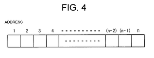
- FIG. 4 is a drawing that schematically shows an example of a storage area in the frame memory 4.
- the frame memory 4 is provided with a storage area assigned to addresses "1" to "n” corresponding to all the pixels, that is, a first pixel to an n-th pixel, of a display panel.
- the frame memory 4 successively overwrites the input video signal of one frame portion of the picture to the addresses "1" to “n” in response to the write signal WR. Accordingly, the stored data is overwritten in order of the addresses "1" to "n” each time the next frame portion of the picture is supplied. And during this time, the frame memory 4 reads out the stored data in order of the addresses "1" to "n” in response to the readout signal RD. In other words, the frame memory 4 successively reads out a video signal corresponding to the first pixel to the n-th pixel of a display panel in the order that it is written.
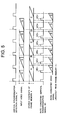
- FIG. 5 shows an example of the operation of the image processor with frame-rate conversion shown in FIG. 1.
- FIG. 5 shows a case in which the rate-converted vertical synchronization signal generating circuit 3 operates with the first conversion coefficient M set to "2" and the second conversion coefficient N set to "3.”
- the rate-converted vertical synchronization signal generating circuit 3 outputs within that period a rate-converted vertical synchronization signal VD consisting of three consecutive pulses. That is, the rate-converted vertical synchronization signal generating circuit 3 outputs a rate-converted vertical synchronization signal VD that is synchronized with the vertical synchronization signal of the input video signal as shown by the dotted lines in FIG. 5, and that has a frequency of (3/2) times that vertical synchronization frequency.
- the frame memory 4 successively overwrites and stores the input video signals corresponding to each frame with a timing corresponding to the vertical synchronization detection signal V to the addresses "1" to "n.”
- the frame memory 4 successively reads out the data stored in the addresses "1" to "n" with a timing that corresponds to the rate-converted vertical synchronization signal VD 1 shown in FIG. 5.
- the rate-converted vertical synchronization signal VD has a higher frequency than the vertical synchronization detection signal V
- the readout speed for the picture frame A is faster than the writing speed for the picture frame B. Accordingly, before the data stored in the frame memory 4 is all overwritten with the video signals corresponding to the picture frame B, the video signals corresponding to the picture frame A are all read out.
- the frame memory 4 again starts the same readout process from the address "1" with a timing corresponding to the rate-converted vertical synchronization signal VD 2 shown in FIG. 5. Then, in the period until the next rate-converted vertical synchronization signal VD 3 is supplied, the video signals of the picture frame B are overwritten and stored in the addresses "1" to "n” of the frame memory 4. Therefore, the reading out from the frame memory 4 of the video signals corresponding to the picture frame B stored in the addresses "1" to "n” is carried out between the rate-converted vertical synchronization signals VD 2 and VD 3 .
- the frame memory 4 starts writing the video signals corresponding to the next picture frame, the picture frame C, with a timing corresponding to the vertical synchronization detection signal V, and also starts reading out in the following manner. Namely, the frame memory 4 reads out the stored data in the addresses from "1" through “n” with a timing corresponding to the rate-converted vertical synchronization signal VD 3 shown in FIG. 5. Since the rate-converted vertical synchronization signal VD has a higher frequency than the vertical synchronization detection signal V, the speed at which the stored picture frame B is read out is faster than the speed at which the data for the picture frame C is overwritten. Accordingly, the video signals corresponding to the picture frame B continue to be read out successively from the frame memory 4.
- the frame memory 4 successively reads out the data stored in the addresses "1" to "n” with a timing corresponding to the rate-converted vertical synchronization signal VD 4 shown in FIG. 5.
- the frame memory 4 carries out the reading out of the video signals corresponding to the picture frame C between the rate-converted vertical synchronization signals VD 4 and VD 5 .
- the frame memory 4 again starts the same readout process from the address "1" with a timing corresponding to the rate-converted vertical synchronization signal VD 5 .
- the video signals of the picture frame D are overwritten and stored in the addresses "1" to "n” of the frame memory 4. Therefore, the reading out from the frame memory 4 of the video signals corresponding to the picture frame D stored in the addresses "1" to "n” is carried out between the rate-converted vertical synchronization signals VD 5 and VD 6 .
- the frame memory 4 starts writing the video signals corresponding to the next picture frame E with a timing corresponding to the vertical synchronization detection signal V, and also starts reading out in the following manner. Namely, the frame memory 4 reads out the stored data in the addresses from "1" through “n” with a timing corresponding to the rate-converted vertical synchronization signal VD 6 shown in FIG. 5. Since the rate-converted vertical synchronization signal VD has a higher frequency than the vertical synchronization detection signal V, the speed at which the stored picture frame D is read out is faster than the speed at which the data for the picture frame E is overwritten. Accordingly, the video signals corresponding to the picture frame D continue to be read out successively from the frame memory 4.
- the vertical synchronization frequency of the video signal is converted to (3/2) times without causing the so-called overrun phenomenon, in which stored data overwrites the video signal of the next frame while being read out from the frame memory. That is, with the frame-rate conversion circuit shown in FIG. 1, it is possible to convert the input video signal to a video signal that has a desired vertical synchronization frequency without (with frame-rate conversion) causing the overrun phenomenon and using a single frame memory.
Abstract
Disclosed is an image processor with frame-rate
conversion that can perform frame-rate conversion of a video
signal with a single frame memory. In this image processor
with frame-rate conversion, input digital video signals are
successively written on the frame memory with a timing
synchronized with a vertical synchronization signal included
in the input digital video signals. During this time, a
frequency signal that mainly consists of a train of N pulses
for every M cycles of the vertical synchronization signal is
generated as a vertical synchronization signal being rate-converted,
and the input digital video signals stored in the
frame memory are read out in the order in which they were
written with a timing synchronized with the vertical
synchronization signal being rate-converted. Such a
configuration makes it possible to convert the input digital
video signals to video signals having a desired vertical
synchronization frequency with use of a single frame memory,
thereby converting frame-rate.
Description
- The present invention relates to image processors with frame-rate conversion that convert input video signals to video signals having a frame-rate (number of frames per second) that is different from the frame-rate of the input video signals.
- A plasma display device equipped with a frame-rate conversion circuit that converts the frame-rate of the input video signal is now being commercialized. For example, a plasma display device disclosed in Japanese Patent Number 3125269 is provided with a frame-rate conversion circuit that performs frame-rate conversion using two frame memories.
- In other words, this frame-rate conversion circuit is configured with first and second frame memories, and a frame memory control means that controls the writing and reading of these first and second frame memories. The frame memory control means performs such a control that, while the input video signals were written on one of the frame memories, video signals are read out from the other frame memory at a readout speed corresponding to a desired vertical synchronization frequency that is different from the vertical synchronization frequency of the input video signals. Accordingly, each time when a vertical synchronization signal is detected in the input video signal, the frame memory control means alternately switches the readout target (or write target) to the appropriate frame memory as noted above. This operation prevents the so-called overrun phenomenon, in which stored data overwrites the video signal of the next frame while being read out from the frame memory, and also makes it possible to convert the input video signals to video signals that has a desired vertical synchronization frequency, thereby converting frame-rate. Since, however, an existing image processor includes two frame memories for such a frame-rate conversion circuit, there is a problem that such image processor is large in a circuit's scale.
- A main object of the present invention is to provide an image processor with frame-rate conversion that can perform frame-rate conversion of video signals with a single frame memory.
- One aspect of the present invention relates to an image processor with frame-rate conversion that generates video signals being rate-converted by converting a vertical synchronization frequency of input digital video signals consisting of successive frames into a desired frequency. This image processor comprises a frame memory having a storage capacity for a single frame of said input digital video signals; a memory write control circuit which successively writes said input digital video signals on said frame memory with a timing synchronized with a vertical synchronization signal included in said input digital video signals; a vertical synchronization signal generating circuit which produces a frequency signal mainly consisting of a train of N pulses (N being a natural number) for every M cycles (M being a natural number) of the vertical synchronization signal, as a vertical synchronization signal being rate-converted, the natural number N being larger than the natural number M; and a memory readout control circuit which reads out and outputs the input digital video signals from said frame memory in the order in which said input digital video signals were written and with a timing synchronized with the vertical synchronization signal being rate-converted, as said video signals being rate-converted.
-
- FIG. 1 shows a configuration of an image processor with frame-rate conversion.
- FIG. 2 shows an example of the waveform of the rate-converted vertical synchronization signal VD generated based on the vertical synchronization detection signal V when the first conversion coefficient M is set to "5" and the second conversion coefficient N is set to "6."
- FIG. 3 shows an example of the waveform of the rate-converted vertical synchronization signal VD generated based on the vertical synchronization detection signal V when the first conversion coefficient M is set to "5" and the second conversion coefficient N is set to "7."
- FIG. 4 is a drawing that schematically shows an example of a storage area in the frame memory.
- FIG. 5 shows an example of the operation of the image processor with frame-rate conversion when the first conversion coefficient M is set to "3" and the second conversion coefficient N is set to "2."
-
- The following are descriptions of embodiments of the present invention with reference to the accompanying drawings.
- FIG. 1 shows a configuration of one embodiment of an image processor with frame-rate conversion according to the present invention.
- As shown in FIG. 1, a synchronization detection circuit 1 generates a vertical synchronization detection signal V each time when a vertical synchronization signal is detected in the input video signal, and supplies the vertical synchronization detection signal V to a memory write control circuit 2 and a rate-converted vertical synchronization signal generating circuit 3. The memory write control circuit 2 generates a write signal WR that indicates the timing of the writing of each pixel synchronized with the vertical synchronization detection signal V, and supplies this write signal WR to a frame memory 4.
- Based on a first conversion coefficient M and a second conversion coefficient N (M and N are positive integers), the rate-converted vertical synchronization signal generating circuit 3 converts the vertical synchronization signal (frequency f1) of the input video signal to a rate-converted vertical synchronization signal VD that has a desired vertical synchronization frequency f2, and outputs this rate-converted vertical synchronization signal with a timing synchronized with the above-mentioned vertical synchronization detection signal V. It should be noted that the second conversion coefficient N is set larger than the first conversion coefficient M, but not more than two times larger than the first conversion coefficient M.
- That is, the rate-converted vertical synchronization signal generating circuit 3 generates the rate-converted vertical synchronization signal VD with a vertical synchronization frequency f2 given by the following expression:
- The rate-converted vertical synchronization signal generating circuit 3 outputs a rate-converted vertical synchronization signal VD at such timing that for each pulse sequence mainly consisting of a train of N pulses in the rate-converted vertical synchronization signal VD, at least one of the pulses in the pulse sequence has the same timing as one of the pulses in the vertical synchronization detection signal V.
- For example, when converting an input video signal with a vertical synchronization signal whose frequency is 50 Hz, such as that of the PAL system television signal, to a video signal with a vertical synchronization frequency of 60 Hz, the first conversion coefficient M is set to "5" and the second conversion coefficient N is set to "6." In this way, the rate-converted vertical synchronization signal generating circuit 3, as shown in FIG. 2, outputs a rate-converted vertical synchronization signal VD, whose frequency is 60 Hz, consisting of six consecutive pulses for every five cycle portions of the vertical synchronization detection signal V, that is, for every period of 5 x (1/50) seconds. One pulse within each of the pulse sequences consisting of six consecutive pulses in the rate-converted vertical synchronization signal VD has the same timing as one pulse in the vertical synchronization detection signal V, as indicated by the dotted lines in FIG. 2. That is, the rate-converted vertical synchronization signal generating circuit 3 outputs the rate-converted vertical synchronization signal VD whose frequency is 60 Hz, synchronized with the vertical synchronization detection signal V whose frequency is 50 Hz.
- Furthermore, when converting an input video signal whose frequency is 50 Hz to a video signal with a vertical synchronization signal whose frequency is 70 Hz, the first conversion coefficient M is set to "5" and the second conversion coefficient N is set to "7." In this way, as shown in FIG. 3, the rate-converted vertical synchronization signal generating circuit 3 outputs a rate-converted vertical synchronization signal VD whose frequency is 70 Hz, consisting of seven consecutive pulses for every five cycles of the vertical synchronization detection signal V, that is, for every period of 5 x (1/50) seconds. One pulse within each of the pulse sequences consisting of seven consecutive pulses in the rate-converted vertical synchronization signal VD has the same timing as one pulse in the vertical synchronization detection signal V, as indicated by the dotted lines in FIG. 3. That is, the rate-converted vertical synchronization signal generating circuit 3 outputs the 70 Hz rate-converted vertical synchronization signal VD synchronized with the 50 Hz vertical synchronization detection signal V.
- Furthermore, when converting an input video signal with a vertical synchronization signal whose frequency is 60 Hz, such as that of the NTSC system television signal, to a video signal with a vertical synchronization signal whose frequency is 72 Hz, the first conversion coefficient M is set to "5" and the second conversion coefficient N is set to "6." In this way, the rate-converted vertical synchronization signal generating circuit 3 outputs a rate-converted vertical synchronization signal VD, whose frequency is 72 Hz, consisting of six consecutive pulses for every five cycles of the vertical synchronization detection signal V, that is, for every period of 5 x (1/60) seconds.
- Furthermore, when the first conversion coefficient M and the second conversion coefficient N are both set to "1," the rate-converted vertical synchronization signal generating circuit 3 outputs a rate-converted vertical synchronization signal VD with the same frequency as the vertical synchronization frequency of the input video signal.
- In this way, in order to obtain a rate-converted vertical synchronization signal VD that has a vertical synchronization frequency of f1 · (N/M) as described above, the rate-converted vertical synchronization signal generating circuit 3 generates a frequency signal consisting of N pulses for every M cycles of the vertical synchronization detection signal V and uses this frequency signal for the rate-converted vertical synchronization signal VD.
- The rate-converted vertical synchronization signal generating circuit 3 then supplies the rate-converted vertical synchronization signal VD to a display panel portion (not shown in drawing) that drives a display panel such as a plasma display panel, an electroluminescence panel, or a liquid crystal panel for example, as well as a memory readout control circuit 5.
- The memory readout control circuit 5 generates a readout signal RD that indicates the timing of the writing of each pixel synchronized with the rate-converted vertical synchronization signal VD, and supplies this to a frame memory 4.
- While successively writing input video signals corresponding to the write signal WR, the frame memory 4 reads out the video signals in the order that they are written corresponding to the readout signal RD, and outputs these video signals as a rate-converted video signal.
- FIG. 4 is a drawing that schematically shows an example of a storage area in the frame memory 4.
- In the example shown in FIG. 4, the frame memory 4 is provided with a storage area assigned to addresses "1" to "n" corresponding to all the pixels, that is, a first pixel to an n-th pixel, of a display panel. The frame memory 4 successively overwrites the input video signal of one frame portion of the picture to the addresses "1" to "n" in response to the write signal WR. Accordingly, the stored data is overwritten in order of the addresses "1" to "n" each time the next frame portion of the picture is supplied. And during this time, the frame memory 4 reads out the stored data in order of the addresses "1" to "n" in response to the readout signal RD. In other words, the frame memory 4 successively reads out a video signal corresponding to the first pixel to the n-th pixel of a display panel in the order that it is written.
- FIG. 5 shows an example of the operation of the image processor with frame-rate conversion shown in FIG. 1.
- It should be noted that FIG. 5 shows a case in which the rate-converted vertical synchronization signal generating circuit 3 operates with the first conversion coefficient M set to "2" and the second conversion coefficient N set to "3."
- As shown in FIG. 5, with these settings, for every two cycles of the vertical synchronization detection signal V, the rate-converted vertical synchronization signal generating circuit 3 outputs within that period a rate-converted vertical synchronization signal VD consisting of three consecutive pulses. That is, the rate-converted vertical synchronization signal generating circuit 3 outputs a rate-converted vertical synchronization signal VD that is synchronized with the vertical synchronization signal of the input video signal as shown by the dotted lines in FIG. 5, and that has a frequency of (3/2) times that vertical synchronization frequency. When input video signals corresponding to a picture frame A, a picture frame B, a picture frame C, ..., and a picture frame E are supplied here as shown in FIG. 5, the frame memory 4 successively overwrites and stores the input video signals corresponding to each frame with a timing corresponding to the vertical synchronization detection signal V to the addresses "1" to "n."
- For example, when the input video signals corresponding to the picture fame A are all stored in the addresses "1" to "n," the input video signals corresponding to the next picture frame, the picture fame B, are supplied, and therefore the stored data corresponding to the picture frame A are gradually overwritten by the data that corresponds to the picture frame B. During this time, the frame memory 4 successively reads out the data stored in the addresses "1" to "n" with a timing that corresponds to the rate-converted vertical synchronization signal VD1 shown in FIG. 5. Although the writing for the picture frame B is being executed at the same time, since the rate-converted vertical synchronization signal VD has a higher frequency than the vertical synchronization detection signal V, the readout speed for the picture frame A is faster than the writing speed for the picture frame B. Accordingly, before the data stored in the frame memory 4 is all overwritten with the video signals corresponding to the picture frame B, the video signals corresponding to the picture frame A are all read out.
- Then, when the reading out of the picture frame A, which was stored in the addresses "1" to "n," is finished, the frame memory 4 again starts the same readout process from the address "1" with a timing corresponding to the rate-converted vertical synchronization signal VD2 shown in FIG. 5. Then, in the period until the next rate-converted vertical synchronization signal VD3 is supplied, the video signals of the picture frame B are overwritten and stored in the addresses "1" to "n" of the frame memory 4. Therefore, the reading out from the frame memory 4 of the video signals corresponding to the picture frame B stored in the addresses "1" to "n" is carried out between the rate-converted vertical synchronization signals VD2 and VD3.
- Then, when the reading out of the picture frame B, which was stored in the addresses "1" to "n," is finished, the frame memory 4 starts writing the video signals corresponding to the next picture frame, the picture frame C, with a timing corresponding to the vertical synchronization detection signal V, and also starts reading out in the following manner. Namely, the frame memory 4 reads out the stored data in the addresses from "1" through "n" with a timing corresponding to the rate-converted vertical synchronization signal VD3 shown in FIG. 5. Since the rate-converted vertical synchronization signal VD has a higher frequency than the vertical synchronization detection signal V, the speed at which the stored picture frame B is read out is faster than the speed at which the data for the picture frame C is overwritten. Accordingly, the video signals corresponding to the picture frame B continue to be read out successively from the frame memory 4.
- Then, when the re-reading out of all the video signals corresponding to the picture frame B is finished, the frame memory 4 successively reads out the data stored in the addresses "1" to "n" with a timing corresponding to the rate-converted vertical synchronization signal VD4 shown in FIG. 5. In the period until the next rate-converted vertical synchronization signal VD5 is supplied, all the video signals of the picture frame C are overwritten and stored in the addresses "1" to "n" of the frame memory 4. Therefore, the frame memory 4 carries out the reading out of the video signals corresponding to the picture frame C between the rate-converted vertical synchronization signals VD4 and VD5.
- Then, when the reading out of the picture frame C, which was stored in the addresses "1" to "n," is finished, the frame memory 4 again starts the same readout process from the address "1" with a timing corresponding to the rate-converted vertical synchronization signal VD5. In the period until the next rate-converted vertical synchronization signal VD6 is supplied, the video signals of the picture frame D are overwritten and stored in the addresses "1" to "n" of the frame memory 4. Therefore, the reading out from the frame memory 4 of the video signals corresponding to the picture frame D stored in the addresses "1" to "n" is carried out between the rate-converted vertical synchronization signals VD5 and VD6.
- Then, when the reading out of the picture frame D, which was stored in the addresses "1" to "n," is finished, the frame memory 4 starts writing the video signals corresponding to the next picture frame E with a timing corresponding to the vertical synchronization detection signal V, and also starts reading out in the following manner. Namely, the frame memory 4 reads out the stored data in the addresses from "1" through "n" with a timing corresponding to the rate-converted vertical synchronization signal VD6 shown in FIG. 5. Since the rate-converted vertical synchronization signal VD has a higher frequency than the vertical synchronization detection signal V, the speed at which the stored picture frame D is read out is faster than the speed at which the data for the picture frame E is overwritten. Accordingly, the video signals corresponding to the picture frame D continue to be read out successively from the frame memory 4.
- With the above-described operation, the vertical synchronization frequency of the video signal is converted to (3/2) times without causing the so-called overrun phenomenon, in which stored data overwrites the video signal of the next frame while being read out from the frame memory. That is, with the frame-rate conversion circuit shown in FIG. 1, it is possible to convert the input video signal to a video signal that has a desired vertical synchronization frequency without (with frame-rate conversion) causing the overrun phenomenon and using a single frame memory.
- It is understood that the foregoing description and accompanying drawings set forth the preferred embodiments of the invention at the present time. Various modifications, additions and alternatives will, of course, become apparent to those skilled in the art in light of the foregoing teachings without departing from the spirit and scope of the disclosed invention. Thus, it should be appreciated that the invention is not limited to the disclosed embodiments but may be practiced within the full scope of the appended claims.
- The features disclosed in the foregoing description, in the claims and/or in the accompanying drawings may, both separately and in any combination thereof, be material for realising the invention in diverse forms thereof.
Claims (2)
- An image processor with frame-rate conversion that generates video signals being rate-converted by converting a vertical synchronization frequency of input digital video signals consisting of successive frames into a desired frequency, said image processor comprising:a frame memory having a storage capacity for a single frame of said input digital video signals;a memory write control circuit which successively writes said input digital video signals on said frame memory with a timing synchronized with a vertical synchronization signal included in said input digital video signals;a vertical synchronization signal generating circuit which produces a frequency signal mainly consisting of a train of N pulses (N being a natural number) for every M cycles (M being a natural number) of the vertical synchronization signal, as a vertical synchronization signal being rate-converted, the natural number N being larger than the natural number M; anda memory readout control circuit which reads out and outputs the input digital video signals from said frame memory in the order in which said input digital video signals were written and with a timing synchronized with the vertical synchronization signal being rate-converted, as said video signals being rate-converted.
- An image processor with frame-rate conversion according to claim 1, wherein the natural number N is smaller than two times the natural number M.
Applications Claiming Priority (2)
| Application Number | Priority Date | Filing Date | Title |
|---|---|---|---|
| JP2003059867A JP2004274219A (en) | 2003-03-06 | 2003-03-06 | Frame rate conversion apparatus for video signal |
| JP2003059867 | 2003-03-06 |
Publications (1)
| Publication Number | Publication Date |
|---|---|
| EP1455338A1 true EP1455338A1 (en) | 2004-09-08 |
Family
ID=32821214
Family Applications (1)
| Application Number | Title | Priority Date | Filing Date |
|---|---|---|---|
| EP04005010A Ceased EP1455338A1 (en) | 2003-03-06 | 2004-03-03 | Image processor with frame-rate conversion |
Country Status (3)
| Country | Link |
|---|---|
| US (1) | US20040183945A1 (en) |
| EP (1) | EP1455338A1 (en) |
| JP (1) | JP2004274219A (en) |
Cited By (2)
| Publication number | Priority date | Publication date | Assignee | Title |
|---|---|---|---|---|
| US8411931B2 (en) | 2006-06-23 | 2013-04-02 | Imax Corporation | Methods and systems for converting 2D motion pictures for stereoscopic 3D exhibition |
| US8842730B2 (en) | 2006-01-27 | 2014-09-23 | Imax Corporation | Methods and systems for digitally re-mastering of 2D and 3D motion pictures for exhibition with enhanced visual quality |
Families Citing this family (10)
| Publication number | Priority date | Publication date | Assignee | Title |
|---|---|---|---|---|
| KR100540228B1 (en) * | 2003-09-04 | 2006-01-10 | 엘지전자 주식회사 | Method for driving a plasma display panel |
| US7817193B2 (en) * | 2004-11-25 | 2010-10-19 | Sony Corporation | Image pickup apparatus and image pickup method to display or record images picked up at high rate in real time |
| JP4887727B2 (en) * | 2005-10-20 | 2012-02-29 | ソニー株式会社 | Image signal processing apparatus, camera system, and image signal processing method |
| JP5174329B2 (en) * | 2006-05-23 | 2013-04-03 | 株式会社日立製作所 | Image processing apparatus and image display apparatus |
| CN100461846C (en) * | 2006-07-31 | 2009-02-11 | 华为技术有限公司 | Method and apparatus of frame frequency conversion |
| CN101572826B (en) * | 2008-04-29 | 2011-07-13 | 深圳迈瑞生物医疗电子股份有限公司 | Ultrasonic video display device and method |
| CN101789236B (en) * | 2009-01-23 | 2013-07-03 | 瑞昱半导体股份有限公司 | Device for controlling input and output of frames |
| JP5821300B2 (en) * | 2011-06-07 | 2015-11-24 | ソニー株式会社 | Imaging apparatus and imaging method |
| JP6708417B2 (en) * | 2016-01-19 | 2020-06-10 | 株式会社Joled | Display device and display device control method |
| CN113132553B (en) * | 2020-01-16 | 2022-07-29 | 京东方科技集团股份有限公司 | Novel source end synchronous display method and device |
Citations (2)
| Publication number | Priority date | Publication date | Assignee | Title |
|---|---|---|---|---|
| US6054980A (en) * | 1999-01-06 | 2000-04-25 | Genesis Microchip, Corp. | Display unit displaying images at a refresh rate less than the rate at which the images are encoded in a received display signal |
| WO2002039737A1 (en) * | 2000-11-07 | 2002-05-16 | Matsushita Electric Industrial Co., Ltd. | Video signal producing system and video signal recording/reproducing device in that system |
Family Cites Families (3)
| Publication number | Priority date | Publication date | Assignee | Title |
|---|---|---|---|---|
| US4532546A (en) * | 1984-01-04 | 1985-07-30 | Itek Corporation | Real time single frame memory for converting video interlaced formats |
| US6222589B1 (en) * | 1996-08-08 | 2001-04-24 | Yves C. Faroudja | Displaying video on high-resolution computer-type monitors substantially without motion discontinuities |
| EP0860081B1 (en) * | 1996-09-11 | 2003-04-02 | Koninklijke Philips Electronics N.V. | Adaptive picture delay |
-
2003
- 2003-03-06 JP JP2003059867A patent/JP2004274219A/en active Pending
-
2004
- 2004-03-02 US US10/790,195 patent/US20040183945A1/en not_active Abandoned
- 2004-03-03 EP EP04005010A patent/EP1455338A1/en not_active Ceased
Patent Citations (3)
| Publication number | Priority date | Publication date | Assignee | Title |
|---|---|---|---|---|
| US6054980A (en) * | 1999-01-06 | 2000-04-25 | Genesis Microchip, Corp. | Display unit displaying images at a refresh rate less than the rate at which the images are encoded in a received display signal |
| WO2002039737A1 (en) * | 2000-11-07 | 2002-05-16 | Matsushita Electric Industrial Co., Ltd. | Video signal producing system and video signal recording/reproducing device in that system |
| US20040081437A1 (en) * | 2000-11-07 | 2004-04-29 | Ryoji Asada | Video signal producing system and video signal recording/ reproducing device in that system |
Cited By (3)
| Publication number | Priority date | Publication date | Assignee | Title |
|---|---|---|---|---|
| US8842730B2 (en) | 2006-01-27 | 2014-09-23 | Imax Corporation | Methods and systems for digitally re-mastering of 2D and 3D motion pictures for exhibition with enhanced visual quality |
| US8411931B2 (en) | 2006-06-23 | 2013-04-02 | Imax Corporation | Methods and systems for converting 2D motion pictures for stereoscopic 3D exhibition |
| US9282313B2 (en) | 2006-06-23 | 2016-03-08 | Imax Corporation | Methods and systems for converting 2D motion pictures for stereoscopic 3D exhibition |
Also Published As
| Publication number | Publication date |
|---|---|
| US20040183945A1 (en) | 2004-09-23 |
| JP2004274219A (en) | 2004-09-30 |
Similar Documents
| Publication | Publication Date | Title |
|---|---|---|
| US8529069B2 (en) | Projection apparatus and control method thereof | |
| EP1455338A1 (en) | Image processor with frame-rate conversion | |
| JP3801242B2 (en) | Reduced image display device | |
| JP6601020B2 (en) | Imaging display device | |
| JP2007049598A (en) | Image processing controller, electronic apparatus and image processing method | |
| JP3384659B2 (en) | Reduced video signal processing circuit | |
| JP2008270937A (en) | Image processing controller, electronic equipment, and image signal processing method | |
| JP2004165912A (en) | Method and device for driving area imaging element | |
| JP2005208413A (en) | Image processor and image display device | |
| JP2002010221A (en) | Image format converting device and imaging apparatus | |
| JP3489852B2 (en) | High-definition imaging device | |
| JP2001057654A (en) | High sensitivity image pickup device | |
| WO2016021162A1 (en) | Image pickup device, image processing device, and image pickup and display device | |
| JP2006154378A (en) | Image display controller | |
| CN115050336A (en) | Display system | |
| JP4525382B2 (en) | Display device and imaging device | |
| KR100396318B1 (en) | Method of processing image data of high pixel density progressive ccd camera | |
| JP3003760B2 (en) | Imaging device | |
| JP2006195134A (en) | Device and method for processing video signal | |
| JPH04156073A (en) | Signal processing system in picture display position converter | |
| JPH11282406A (en) | Driving device for display panel | |
| JPH1198469A (en) | Image processing unit | |
| JP2000020708A (en) | Processor for improving resolution of video data | |
| JPH07327241A (en) | Video display device | |
| JPH11205731A (en) | Digital camera |
Legal Events
| Date | Code | Title | Description |
|---|---|---|---|
| PUAI | Public reference made under article 153(3) epc to a published international application that has entered the european phase |
Free format text: ORIGINAL CODE: 0009012 |
|
| AK | Designated contracting states |
Kind code of ref document: A1 Designated state(s): AT BE BG CH CY CZ DE DK EE ES FI FR GB GR HU IE IT LI LU MC NL PL PT RO SE SI SK TR |
|
| AX | Request for extension of the european patent |
Extension state: AL LT LV MK |
|
| 17P | Request for examination filed |
Effective date: 20040823 |
|
| 17Q | First examination report despatched |
Effective date: 20050120 |
|
| AKX | Designation fees paid |
Designated state(s): DE FR GB |
|
| STAA | Information on the status of an ep patent application or granted ep patent |
Free format text: STATUS: THE APPLICATION HAS BEEN REFUSED |
|
| 18R | Application refused |
Effective date: 20070326 |