EP1480280A2 - Organic electroluminescent device and method for manufacturing the same - Google Patents
Organic electroluminescent device and method for manufacturing the same Download PDFInfo
- Publication number
- EP1480280A2 EP1480280A2 EP04011981A EP04011981A EP1480280A2 EP 1480280 A2 EP1480280 A2 EP 1480280A2 EP 04011981 A EP04011981 A EP 04011981A EP 04011981 A EP04011981 A EP 04011981A EP 1480280 A2 EP1480280 A2 EP 1480280A2
- Authority
- EP
- European Patent Office
- Prior art keywords
- electrode
- auxiliary electrode
- organic
- transparent electrode
- layer
- Prior art date
- Legal status (The legal status is an assumption and is not a legal conclusion. Google has not performed a legal analysis and makes no representation as to the accuracy of the status listed.)
- Withdrawn
Links
- 238000000034 method Methods 0.000 title claims description 33
- 238000004519 manufacturing process Methods 0.000 title claims description 5
- 239000000463 material Substances 0.000 claims abstract description 123
- 239000012044 organic layer Substances 0.000 claims abstract description 81
- 239000007789 gas Substances 0.000 claims description 27
- 238000009499 grossing Methods 0.000 claims description 11
- 229910052782 aluminium Inorganic materials 0.000 claims description 8
- XAGFODPZIPBFFR-UHFFFAOYSA-N aluminium Chemical compound [Al] XAGFODPZIPBFFR-UHFFFAOYSA-N 0.000 claims description 8
- 238000002834 transmittance Methods 0.000 claims description 8
- QVGXLLKOCUKJST-UHFFFAOYSA-N atomic oxygen Chemical compound [O] QVGXLLKOCUKJST-UHFFFAOYSA-N 0.000 claims description 5
- 239000001301 oxygen Substances 0.000 claims description 5
- 229910052760 oxygen Inorganic materials 0.000 claims description 5
- XKRFYHLGVUSROY-UHFFFAOYSA-N Argon Chemical compound [Ar] XKRFYHLGVUSROY-UHFFFAOYSA-N 0.000 claims description 4
- 229910052786 argon Inorganic materials 0.000 claims description 4
- 239000010410 layer Substances 0.000 description 178
- 238000002347 injection Methods 0.000 description 94
- 239000007924 injection Substances 0.000 description 94
- 230000032258 transport Effects 0.000 description 70
- 239000000758 substrate Substances 0.000 description 34
- 238000004544 sputter deposition Methods 0.000 description 30
- 239000000126 substance Substances 0.000 description 23
- 229910052751 metal Inorganic materials 0.000 description 22
- 230000008569 process Effects 0.000 description 22
- 239000002184 metal Substances 0.000 description 21
- 238000007740 vapor deposition Methods 0.000 description 21
- 238000009832 plasma treatment Methods 0.000 description 20
- 230000003746 surface roughness Effects 0.000 description 20
- 230000000052 comparative effect Effects 0.000 description 18
- 239000002019 doping agent Substances 0.000 description 18
- 239000000203 mixture Substances 0.000 description 18
- UHOVQNZJYSORNB-UHFFFAOYSA-N Benzene Chemical compound C1=CC=CC=C1 UHOVQNZJYSORNB-UHFFFAOYSA-N 0.000 description 15
- 238000006243 chemical reaction Methods 0.000 description 14
- -1 cobalt silicide Chemical compound 0.000 description 14
- 230000015572 biosynthetic process Effects 0.000 description 10
- 229910045601 alloy Inorganic materials 0.000 description 9
- 239000000956 alloy Substances 0.000 description 9
- ZYGHJZDHTFUPRJ-UHFFFAOYSA-N coumarin Chemical class C1=CC=C2OC(=O)C=CC2=C1 ZYGHJZDHTFUPRJ-UHFFFAOYSA-N 0.000 description 9
- 239000000975 dye Substances 0.000 description 9
- IEQIEDJGQAUEQZ-UHFFFAOYSA-N phthalocyanine Chemical class N1C(N=C2C3=CC=CC=C3C(N=C3C4=CC=CC=C4C(=N4)N3)=N2)=C(C=CC=C2)C2=C1N=C1C2=CC=CC=C2C4=N1 IEQIEDJGQAUEQZ-UHFFFAOYSA-N 0.000 description 9
- 239000010409 thin film Substances 0.000 description 9
- 239000007983 Tris buffer Substances 0.000 description 8
- 150000001875 compounds Chemical class 0.000 description 8
- 239000010408 film Substances 0.000 description 8
- 238000000151 deposition Methods 0.000 description 7
- 238000005401 electroluminescence Methods 0.000 description 7
- 150000002739 metals Chemical class 0.000 description 7
- 229960003540 oxyquinoline Drugs 0.000 description 7
- MCJGNVYPOGVAJF-UHFFFAOYSA-N quinolin-8-ol Chemical compound C1=CN=C2C(O)=CC=CC2=C1 MCJGNVYPOGVAJF-UHFFFAOYSA-N 0.000 description 7
- 229920005989 resin Polymers 0.000 description 7
- 239000011347 resin Substances 0.000 description 7
- XOLBLPGZBRYERU-UHFFFAOYSA-N tin dioxide Chemical compound O=[Sn]=O XOLBLPGZBRYERU-UHFFFAOYSA-N 0.000 description 7
- 230000004888 barrier function Effects 0.000 description 6
- 230000007423 decrease Effects 0.000 description 6
- 230000005283 ground state Effects 0.000 description 6
- XLOMVQKBTHCTTD-UHFFFAOYSA-N Zinc monoxide Chemical compound [Zn]=O XLOMVQKBTHCTTD-UHFFFAOYSA-N 0.000 description 5
- 230000008021 deposition Effects 0.000 description 5
- 230000005284 excitation Effects 0.000 description 5
- 239000011521 glass Substances 0.000 description 5
- 229910003437 indium oxide Inorganic materials 0.000 description 5
- PJXISJQVUVHSOJ-UHFFFAOYSA-N indium(iii) oxide Chemical compound [O-2].[O-2].[O-2].[In+3].[In+3] PJXISJQVUVHSOJ-UHFFFAOYSA-N 0.000 description 5
- 239000011777 magnesium Substances 0.000 description 5
- 238000002156 mixing Methods 0.000 description 5
- 125000002924 primary amino group Chemical group [H]N([H])* 0.000 description 5
- 239000011241 protective layer Substances 0.000 description 5
- 238000004528 spin coating Methods 0.000 description 5
- OKTJSMMVPCPJKN-UHFFFAOYSA-N Carbon Chemical compound [C] OKTJSMMVPCPJKN-UHFFFAOYSA-N 0.000 description 4
- JUJWROOIHBZHMG-UHFFFAOYSA-N Pyridine Chemical compound C1=CC=NC=C1 JUJWROOIHBZHMG-UHFFFAOYSA-N 0.000 description 4
- YTPLMLYBLZKORZ-UHFFFAOYSA-N Thiophene Chemical compound C=1C=CSC=1 YTPLMLYBLZKORZ-UHFFFAOYSA-N 0.000 description 4
- NRTOMJZYCJJWKI-UHFFFAOYSA-N Titanium nitride Chemical compound [Ti]#N NRTOMJZYCJJWKI-UHFFFAOYSA-N 0.000 description 4
- IOJUPLGTWVMSFF-UHFFFAOYSA-N benzothiazole Chemical compound C1=CC=C2SC=NC2=C1 IOJUPLGTWVMSFF-UHFFFAOYSA-N 0.000 description 4
- 229910052799 carbon Inorganic materials 0.000 description 4
- 229910052804 chromium Inorganic materials 0.000 description 4
- 239000011651 chromium Substances 0.000 description 4
- 239000011261 inert gas Substances 0.000 description 4
- PQXKHYXIUOZZFA-UHFFFAOYSA-M lithium fluoride Chemical compound [Li+].[F-] PQXKHYXIUOZZFA-UHFFFAOYSA-M 0.000 description 4
- 125000002080 perylenyl group Chemical group C1(=CC=C2C=CC=C3C4=CC=CC5=CC=CC(C1=C23)=C45)* 0.000 description 4
- 229920000642 polymer Polymers 0.000 description 4
- 238000012546 transfer Methods 0.000 description 4
- 230000007704 transition Effects 0.000 description 4
- 238000011282 treatment Methods 0.000 description 4
- UWRZIZXBOLBCON-VOTSOKGWSA-N (e)-2-phenylethenamine Chemical class N\C=C\C1=CC=CC=C1 UWRZIZXBOLBCON-VOTSOKGWSA-N 0.000 description 3
- NGQSLSMAEVWNPU-YTEMWHBBSA-N 1,2-bis[(e)-2-phenylethenyl]benzene Chemical compound C=1C=CC=CC=1/C=C/C1=CC=CC=C1\C=C\C1=CC=CC=C1 NGQSLSMAEVWNPU-YTEMWHBBSA-N 0.000 description 3
- BCMCBBGGLRIHSE-UHFFFAOYSA-N 1,3-benzoxazole Chemical compound C1=CC=C2OC=NC2=C1 BCMCBBGGLRIHSE-UHFFFAOYSA-N 0.000 description 3
- 239000005725 8-Hydroxyquinoline Substances 0.000 description 3
- QTBSBXVTEAMEQO-UHFFFAOYSA-N Acetic acid Chemical compound CC(O)=O QTBSBXVTEAMEQO-UHFFFAOYSA-N 0.000 description 3
- PNEYBMLMFCGWSK-UHFFFAOYSA-N Alumina Chemical compound [O-2].[O-2].[O-2].[Al+3].[Al+3] PNEYBMLMFCGWSK-UHFFFAOYSA-N 0.000 description 3
- VYZAMTAEIAYCRO-UHFFFAOYSA-N Chromium Chemical group [Cr] VYZAMTAEIAYCRO-UHFFFAOYSA-N 0.000 description 3
- RYGMFSIKBFXOCR-UHFFFAOYSA-N Copper Chemical compound [Cu] RYGMFSIKBFXOCR-UHFFFAOYSA-N 0.000 description 3
- KWYHDKDOAIKMQN-UHFFFAOYSA-N N,N,N',N'-tetramethylethylenediamine Chemical compound CN(C)CCN(C)C KWYHDKDOAIKMQN-UHFFFAOYSA-N 0.000 description 3
- PAYRUJLWNCNPSJ-UHFFFAOYSA-N N-phenyl amine Natural products NC1=CC=CC=C1 PAYRUJLWNCNPSJ-UHFFFAOYSA-N 0.000 description 3
- NRCMAYZCPIVABH-UHFFFAOYSA-N Quinacridone Chemical class N1C2=CC=CC=C2C(=O)C2=C1C=C1C(=O)C3=CC=CC=C3NC1=C2 NRCMAYZCPIVABH-UHFFFAOYSA-N 0.000 description 3
- 229910052783 alkali metal Inorganic materials 0.000 description 3
- 150000001339 alkali metal compounds Chemical class 0.000 description 3
- 150000001340 alkali metals Chemical class 0.000 description 3
- 125000003118 aryl group Chemical group 0.000 description 3
- 239000011575 calcium Chemical group 0.000 description 3
- 238000004140 cleaning Methods 0.000 description 3
- 229910052802 copper Inorganic materials 0.000 description 3
- 239000010949 copper Substances 0.000 description 3
- 229960000956 coumarin Drugs 0.000 description 3
- 235000001671 coumarin Nutrition 0.000 description 3
- 238000005530 etching Methods 0.000 description 3
- 230000005281 excited state Effects 0.000 description 3
- 150000002222 fluorine compounds Chemical class 0.000 description 3
- 230000005525 hole transport Effects 0.000 description 3
- 239000011133 lead Substances 0.000 description 3
- FUJCRWPEOMXPAD-UHFFFAOYSA-N lithium oxide Chemical compound [Li+].[Li+].[O-2] FUJCRWPEOMXPAD-UHFFFAOYSA-N 0.000 description 3
- 229910001947 lithium oxide Inorganic materials 0.000 description 3
- VNWKTOKETHGBQD-UHFFFAOYSA-N methane Chemical compound C VNWKTOKETHGBQD-UHFFFAOYSA-N 0.000 description 3
- 150000004767 nitrides Chemical class 0.000 description 3
- 229910052757 nitrogen Inorganic materials 0.000 description 3
- 239000011368 organic material Substances 0.000 description 3
- 150000004866 oxadiazoles Chemical class 0.000 description 3
- 125000001997 phenyl group Chemical group [H]C1=C([H])C([H])=C(*)C([H])=C1[H] 0.000 description 3
- 238000012545 processing Methods 0.000 description 3
- 238000001552 radio frequency sputter deposition Methods 0.000 description 3
- PJANXHGTPQOBST-UHFFFAOYSA-N stilbene Chemical class C=1C=CC=CC=1C=CC1=CC=CC=C1 PJANXHGTPQOBST-UHFFFAOYSA-N 0.000 description 3
- 229940042055 systemic antimycotics triazole derivative Drugs 0.000 description 3
- 238000012360 testing method Methods 0.000 description 3
- 239000011135 tin Substances 0.000 description 3
- 229910052718 tin Inorganic materials 0.000 description 3
- TVIVIEFSHFOWTE-UHFFFAOYSA-K tri(quinolin-8-yloxy)alumane Chemical compound [Al+3].C1=CN=C2C([O-])=CC=CC2=C1.C1=CN=C2C([O-])=CC=CC2=C1.C1=CN=C2C([O-])=CC=CC2=C1 TVIVIEFSHFOWTE-UHFFFAOYSA-K 0.000 description 3
- 125000005259 triarylamine group Chemical class 0.000 description 3
- 229910052721 tungsten Inorganic materials 0.000 description 3
- 238000001039 wet etching Methods 0.000 description 3
- 229910052725 zinc Inorganic materials 0.000 description 3
- 239000011701 zinc Substances 0.000 description 3
- KLCLIOISYBHYDZ-UHFFFAOYSA-N 1,4,4-triphenylbuta-1,3-dienylbenzene Chemical class C=1C=CC=CC=1C(C=1C=CC=CC=1)=CC=C(C=1C=CC=CC=1)C1=CC=CC=C1 KLCLIOISYBHYDZ-UHFFFAOYSA-N 0.000 description 2
- UHXOHPVVEHBKKT-UHFFFAOYSA-N 1-(2,2-diphenylethenyl)-4-[4-(2,2-diphenylethenyl)phenyl]benzene Chemical group C=1C=C(C=2C=CC(C=C(C=3C=CC=CC=3)C=3C=CC=CC=3)=CC=2)C=CC=1C=C(C=1C=CC=CC=1)C1=CC=CC=C1 UHXOHPVVEHBKKT-UHFFFAOYSA-N 0.000 description 2
- SULWTXOWAFVWOY-PHEQNACWSA-N 2,3-bis[(E)-2-phenylethenyl]pyrazine Chemical class C=1C=CC=CC=1/C=C/C1=NC=CN=C1\C=C\C1=CC=CC=C1 SULWTXOWAFVWOY-PHEQNACWSA-N 0.000 description 2
- OGGKVJMNFFSDEV-UHFFFAOYSA-N 3-methyl-n-[4-[4-(n-(3-methylphenyl)anilino)phenyl]phenyl]-n-phenylaniline Chemical group CC1=CC=CC(N(C=2C=CC=CC=2)C=2C=CC(=CC=2)C=2C=CC(=CC=2)N(C=2C=CC=CC=2)C=2C=C(C)C=CC=2)=C1 OGGKVJMNFFSDEV-UHFFFAOYSA-N 0.000 description 2
- HSHNITRMYYLLCV-UHFFFAOYSA-N 4-methylumbelliferone Chemical compound C1=C(O)C=CC2=C1OC(=O)C=C2C HSHNITRMYYLLCV-UHFFFAOYSA-N 0.000 description 2
- IYBLVRRCNVHZQJ-UHFFFAOYSA-N 5-Hydroxyflavone Chemical compound C=1C(=O)C=2C(O)=CC=CC=2OC=1C1=CC=CC=C1 IYBLVRRCNVHZQJ-UHFFFAOYSA-N 0.000 description 2
- LRFVTYWOQMYALW-UHFFFAOYSA-N 9H-xanthine Chemical compound O=C1NC(=O)NC2=C1NC=N2 LRFVTYWOQMYALW-UHFFFAOYSA-N 0.000 description 2
- IJGRMHOSHXDMSA-UHFFFAOYSA-N Atomic nitrogen Chemical compound N#N IJGRMHOSHXDMSA-UHFFFAOYSA-N 0.000 description 2
- 150000000918 Europium Chemical class 0.000 description 2
- 101000679365 Homo sapiens Putative tyrosine-protein phosphatase TPTE Proteins 0.000 description 2
- UQSXHKLRYXJYBZ-UHFFFAOYSA-N Iron oxide Chemical compound [Fe]=O UQSXHKLRYXJYBZ-UHFFFAOYSA-N 0.000 description 2
- FYYHWMGAXLPEAU-UHFFFAOYSA-N Magnesium Chemical compound [Mg] FYYHWMGAXLPEAU-UHFFFAOYSA-N 0.000 description 2
- URLKBWYHVLBVBO-UHFFFAOYSA-N Para-Xylene Chemical group CC1=CC=C(C)C=C1 URLKBWYHVLBVBO-UHFFFAOYSA-N 0.000 description 2
- NBIIXXVUZAFLBC-UHFFFAOYSA-N Phosphoric acid Chemical compound OP(O)(O)=O NBIIXXVUZAFLBC-UHFFFAOYSA-N 0.000 description 2
- ISZWRZGKEWQACU-UHFFFAOYSA-N Primuletin Natural products OC1=CC=CC(C=2OC3=CC=CC=C3C(=O)C=2)=C1 ISZWRZGKEWQACU-UHFFFAOYSA-N 0.000 description 2
- 102100022578 Putative tyrosine-protein phosphatase TPTE Human genes 0.000 description 2
- KYQCOXFCLRTKLS-UHFFFAOYSA-N Pyrazine Chemical compound C1=CN=CC=N1 KYQCOXFCLRTKLS-UHFFFAOYSA-N 0.000 description 2
- PJANXHGTPQOBST-VAWYXSNFSA-N Stilbene Natural products C=1C=CC=CC=1/C=C/C1=CC=CC=C1 PJANXHGTPQOBST-VAWYXSNFSA-N 0.000 description 2
- HCHKCACWOHOZIP-UHFFFAOYSA-N Zinc Chemical compound [Zn] HCHKCACWOHOZIP-UHFFFAOYSA-N 0.000 description 2
- MWPLVEDNUUSJAV-UHFFFAOYSA-N anthracene Chemical compound C1=CC=CC2=CC3=CC=CC=C3C=C21 MWPLVEDNUUSJAV-UHFFFAOYSA-N 0.000 description 2
- 150000001454 anthracenes Chemical class 0.000 description 2
- 150000001562 benzopyrans Chemical class 0.000 description 2
- 239000004305 biphenyl Substances 0.000 description 2
- 238000005229 chemical vapour deposition Methods 0.000 description 2
- UUAGAQFQZIEFAH-UHFFFAOYSA-N chlorotrifluoroethylene Chemical group FC(F)=C(F)Cl UUAGAQFQZIEFAH-UHFFFAOYSA-N 0.000 description 2
- 239000011248 coating agent Substances 0.000 description 2
- 238000000576 coating method Methods 0.000 description 2
- 229910000428 cobalt oxide Inorganic materials 0.000 description 2
- IVMYJDGYRUAWML-UHFFFAOYSA-N cobalt(ii) oxide Chemical compound [Co]=O IVMYJDGYRUAWML-UHFFFAOYSA-N 0.000 description 2
- 239000003086 colorant Substances 0.000 description 2
- 229920001577 copolymer Polymers 0.000 description 2
- VPUGDVKSAQVFFS-UHFFFAOYSA-N coronene Chemical compound C1=C(C2=C34)C=CC3=CC=C(C=C3)C4=C4C3=CC=C(C=C3)C4=C2C3=C1 VPUGDVKSAQVFFS-UHFFFAOYSA-N 0.000 description 2
- 230000003247 decreasing effect Effects 0.000 description 2
- 230000007812 deficiency Effects 0.000 description 2
- QDGONURINHVBEW-UHFFFAOYSA-N dichlorodifluoroethylene Chemical group FC(F)=C(Cl)Cl QDGONURINHVBEW-UHFFFAOYSA-N 0.000 description 2
- ZUOUZKKEUPVFJK-UHFFFAOYSA-N diphenyl Chemical compound C1=CC=CC=C1C1=CC=CC=C1 ZUOUZKKEUPVFJK-UHFFFAOYSA-N 0.000 description 2
- 230000002708 enhancing effect Effects 0.000 description 2
- 238000011156 evaluation Methods 0.000 description 2
- 150000008376 fluorenones Chemical class 0.000 description 2
- NBVXSUQYWXRMNV-UHFFFAOYSA-N fluoromethane Chemical compound FC NBVXSUQYWXRMNV-UHFFFAOYSA-N 0.000 description 2
- RBTKNAXYKSUFRK-UHFFFAOYSA-N heliogen blue Chemical compound [Cu].[N-]1C2=C(C=CC=C3)C3=C1N=C([N-]1)C3=CC=CC=C3C1=NC([N-]1)=C(C=CC=C3)C3=C1N=C([N-]1)C3=CC=CC=C3C1=N2 RBTKNAXYKSUFRK-UHFFFAOYSA-N 0.000 description 2
- 150000007857 hydrazones Chemical class 0.000 description 2
- 229910052738 indium Inorganic materials 0.000 description 2
- APFVFJFRJDLVQX-UHFFFAOYSA-N indium atom Chemical compound [In] APFVFJFRJDLVQX-UHFFFAOYSA-N 0.000 description 2
- 229910010272 inorganic material Inorganic materials 0.000 description 2
- 239000011147 inorganic material Substances 0.000 description 2
- 238000007733 ion plating Methods 0.000 description 2
- UEEXRMUCXBPYOV-UHFFFAOYSA-N iridium;2-phenylpyridine Chemical compound [Ir].C1=CC=CC=C1C1=CC=CC=N1.C1=CC=CC=C1C1=CC=CC=N1.C1=CC=CC=C1C1=CC=CC=N1 UEEXRMUCXBPYOV-UHFFFAOYSA-N 0.000 description 2
- 229910052749 magnesium Inorganic materials 0.000 description 2
- 238000012986 modification Methods 0.000 description 2
- 230000004048 modification Effects 0.000 description 2
- 239000003921 oil Substances 0.000 description 2
- 229920000620 organic polymer Polymers 0.000 description 2
- 238000002161 passivation Methods 0.000 description 2
- YNPNZTXNASCQKK-UHFFFAOYSA-N phenanthrene Chemical compound C1=CC=C2C3=CC=CC=C3C=CC2=C1 YNPNZTXNASCQKK-UHFFFAOYSA-N 0.000 description 2
- 239000002861 polymer material Substances 0.000 description 2
- BBEAQIROQSPTKN-UHFFFAOYSA-N pyrene Chemical compound C1=CC=C2C=CC3=CC=CC4=CC=C1C2=C43 BBEAQIROQSPTKN-UHFFFAOYSA-N 0.000 description 2
- 150000003220 pyrenes Chemical class 0.000 description 2
- UMJSCPRVCHMLSP-UHFFFAOYSA-N pyridine Natural products COC1=CC=CN=C1 UMJSCPRVCHMLSP-UHFFFAOYSA-N 0.000 description 2
- PYWVYCXTNDRMGF-UHFFFAOYSA-N rhodamine B Chemical class [Cl-].C=12C=CC(=[N+](CC)CC)C=C2OC2=CC(N(CC)CC)=CC=C2C=1C1=CC=CC=C1C(O)=O PYWVYCXTNDRMGF-UHFFFAOYSA-N 0.000 description 2
- YYMBJDOZVAITBP-UHFFFAOYSA-N rubrene Chemical class C1=CC=CC=C1C(C1=C(C=2C=CC=CC=2)C2=CC=CC=C2C(C=2C=CC=CC=2)=C11)=C(C=CC=C2)C2=C1C1=CC=CC=C1 YYMBJDOZVAITBP-UHFFFAOYSA-N 0.000 description 2
- 238000007789 sealing Methods 0.000 description 2
- 229910021332 silicide Inorganic materials 0.000 description 2
- FVBUAEGBCNSCDD-UHFFFAOYSA-N silicide(4-) Chemical compound [Si-4] FVBUAEGBCNSCDD-UHFFFAOYSA-N 0.000 description 2
- 229910052710 silicon Inorganic materials 0.000 description 2
- 229920002050 silicone resin Polymers 0.000 description 2
- 239000000243 solution Substances 0.000 description 2
- 235000021286 stilbenes Nutrition 0.000 description 2
- 229930192474 thiophene Natural products 0.000 description 2
- 239000010936 titanium Substances 0.000 description 2
- 229910052719 titanium Inorganic materials 0.000 description 2
- ODHXBMXNKOYIBV-UHFFFAOYSA-N triphenylamine Chemical compound C1=CC=CC=C1N(C=1C=CC=CC=1)C1=CC=CC=C1 ODHXBMXNKOYIBV-UHFFFAOYSA-N 0.000 description 2
- 239000010937 tungsten Substances 0.000 description 2
- 238000005019 vapor deposition process Methods 0.000 description 2
- XLYOFNOQVPJJNP-UHFFFAOYSA-N water Substances O XLYOFNOQVPJJNP-UHFFFAOYSA-N 0.000 description 2
- 239000011787 zinc oxide Substances 0.000 description 2
- 229910052726 zirconium Inorganic materials 0.000 description 2
- QKLPIYTUUFFRLV-YTEMWHBBSA-N 1,4-bis[(e)-2-(2-methylphenyl)ethenyl]benzene Chemical compound CC1=CC=CC=C1\C=C\C(C=C1)=CC=C1\C=C\C1=CC=CC=C1C QKLPIYTUUFFRLV-YTEMWHBBSA-N 0.000 description 1
- BCASZEAAHJEDAL-PHEQNACWSA-N 1,4-bis[(e)-2-(4-methylphenyl)ethenyl]benzene Chemical compound C1=CC(C)=CC=C1\C=C\C(C=C1)=CC=C1\C=C\C1=CC=C(C)C=C1 BCASZEAAHJEDAL-PHEQNACWSA-N 0.000 description 1
- LWGPQZLNJIVUIC-UHFFFAOYSA-N 1,4-bis[2-(2-ethylphenyl)ethenyl]benzene Chemical compound CCC1=CC=CC=C1C=CC(C=C1)=CC=C1C=CC1=CC=CC=C1CC LWGPQZLNJIVUIC-UHFFFAOYSA-N 0.000 description 1
- SWYYRSGBEBXIRE-UHFFFAOYSA-N 1,4-bis[2-(3-ethylphenyl)ethenyl]benzene Chemical compound CCC1=CC=CC(C=CC=2C=CC(C=CC=3C=C(CC)C=CC=3)=CC=2)=C1 SWYYRSGBEBXIRE-UHFFFAOYSA-N 0.000 description 1
- VERMWGQSKPXSPZ-BUHFOSPRSA-N 1-[(e)-2-phenylethenyl]anthracene Chemical class C=1C=CC2=CC3=CC=CC=C3C=C2C=1\C=C\C1=CC=CC=C1 VERMWGQSKPXSPZ-BUHFOSPRSA-N 0.000 description 1
- NVZWEEGUWXZOKI-UHFFFAOYSA-N 1-ethenyl-2-methylbenzene Chemical compound CC1=CC=CC=C1C=C NVZWEEGUWXZOKI-UHFFFAOYSA-N 0.000 description 1
- DPFGGYIWNDCEJM-UHFFFAOYSA-N 1-n,1-n,3-n,3-n,5-n,5-n-hexakis-phenylbenzene-1,3,5-triamine Chemical compound C1=CC=CC=C1N(C=1C=C(C=C(C=1)N(C=1C=CC=CC=1)C=1C=CC=CC=1)N(C=1C=CC=CC=1)C=1C=CC=CC=1)C1=CC=CC=C1 DPFGGYIWNDCEJM-UHFFFAOYSA-N 0.000 description 1
- OLUMNEXGMXIAMJ-UHFFFAOYSA-N 1-n,1-n,4-n-triphenyl-4-n-[4-(n-[4-(n-phenylanilino)phenyl]anilino)phenyl]benzene-1,4-diamine Chemical compound C1=CC=CC=C1N(C=1C=CC(=CC=1)N(C=1C=CC=CC=1)C=1C=CC(=CC=1)N(C=1C=CC=CC=1)C=1C=CC(=CC=1)N(C=1C=CC=CC=1)C=1C=CC=CC=1)C1=CC=CC=C1 OLUMNEXGMXIAMJ-UHFFFAOYSA-N 0.000 description 1
- HXWQJYVUJPBQEW-VAWYXSNFSA-N 1-phenyl-4-[(e)-2-(4-phenylphenyl)ethenyl]benzene Chemical compound C=1C=C(C=2C=CC=CC=2)C=CC=1/C=C/C(C=C1)=CC=C1C1=CC=CC=C1 HXWQJYVUJPBQEW-VAWYXSNFSA-N 0.000 description 1
- YEBQUUKDSJCPIX-UHFFFAOYSA-N 12h-benzo[a]thioxanthene Chemical class C1=CC=CC2=C3CC4=CC=CC=C4SC3=CC=C21 YEBQUUKDSJCPIX-UHFFFAOYSA-N 0.000 description 1
- HYZJCKYKOHLVJF-UHFFFAOYSA-N 1H-benzimidazole Chemical compound C1=CC=C2NC=NC2=C1 HYZJCKYKOHLVJF-UHFFFAOYSA-N 0.000 description 1
- UIWLITBBFICQKW-UHFFFAOYSA-N 1h-benzo[h]quinolin-2-one Chemical compound C1=CC=C2C3=NC(O)=CC=C3C=CC2=C1 UIWLITBBFICQKW-UHFFFAOYSA-N 0.000 description 1
- YTDHEFNWWHSXSU-UHFFFAOYSA-N 2,3,5,6-tetrachloroaniline Chemical compound NC1=C(Cl)C(Cl)=CC(Cl)=C1Cl YTDHEFNWWHSXSU-UHFFFAOYSA-N 0.000 description 1
- MVWPVABZQQJTPL-UHFFFAOYSA-N 2,3-diphenylcyclohexa-2,5-diene-1,4-dione Chemical class O=C1C=CC(=O)C(C=2C=CC=CC=2)=C1C1=CC=CC=C1 MVWPVABZQQJTPL-UHFFFAOYSA-N 0.000 description 1
- FZORBZJJXZJZDC-UHFFFAOYSA-N 2,5-bis(2-naphthalen-1-ylethenyl)pyrazine Chemical compound C1=CC=C2C(C=CC3=NC=C(N=C3)C=CC=3C4=CC=CC=C4C=CC=3)=CC=CC2=C1 FZORBZJJXZJZDC-UHFFFAOYSA-N 0.000 description 1
- OWTKICLARQLANW-UHFFFAOYSA-N 2,5-bis(2-pyren-1-ylethenyl)pyrazine Chemical compound C1=C2C(C=CC3=NC=C(N=C3)C=CC=3C4=CC=C5C=CC=C6C=CC(C4=C65)=CC=3)=CC=C(C=C3)C2=C2C3=CC=CC2=C1 OWTKICLARQLANW-UHFFFAOYSA-N 0.000 description 1
- ZGXQLVRLPJXTIK-LQIBPGRFSA-N 2,5-bis[(e)-2-(4-methoxyphenyl)ethenyl]pyrazine Chemical compound C1=CC(OC)=CC=C1\C=C\C(N=C1)=CN=C1\C=C\C1=CC=C(OC)C=C1 ZGXQLVRLPJXTIK-LQIBPGRFSA-N 0.000 description 1
- PAJSTGVSGZWCGO-UHFFFAOYSA-N 2,5-bis[2-(4-ethylphenyl)ethenyl]pyrazine Chemical compound C1=CC(CC)=CC=C1C=CC(N=C1)=CN=C1C=CC1=CC=C(CC)C=C1 PAJSTGVSGZWCGO-UHFFFAOYSA-N 0.000 description 1
- BFQSAUNFPAHVRZ-UHFFFAOYSA-N 2,5-bis[2-(4-methylphenyl)ethenyl]pyrazine Chemical compound C1=CC(C)=CC=C1C=CC(N=C1)=CN=C1C=CC1=CC=C(C)C=C1 BFQSAUNFPAHVRZ-UHFFFAOYSA-N 0.000 description 1
- NBYLBWHHTUWMER-UHFFFAOYSA-N 2-Methylquinolin-8-ol Chemical compound C1=CC=C(O)C2=NC(C)=CC=C21 NBYLBWHHTUWMER-UHFFFAOYSA-N 0.000 description 1
- BDMRRCGWWDZRRG-UHFFFAOYSA-N 2-[2-(4-chlorophenyl)ethenyl]benzo[e][1,3]benzoxazole Chemical compound C1=CC(Cl)=CC=C1C=CC(O1)=NC2=C1C=CC1=CC=CC=C21 BDMRRCGWWDZRRG-UHFFFAOYSA-N 0.000 description 1
- PORKWWLSRFDCLR-UHFFFAOYSA-N 2-[2-[4-[2-(1,3-benzothiazol-2-yl)ethenyl]phenyl]ethenyl]-1,3-benzothiazole Chemical compound C1=CC=C2SC(C=CC=3C=CC(C=CC=4SC5=CC=CC=C5N=4)=CC=3)=NC2=C1 PORKWWLSRFDCLR-UHFFFAOYSA-N 0.000 description 1
- JDDDDNVALGZAMR-UHFFFAOYSA-N 2-[4-[2-(1h-benzimidazol-2-yl)ethenyl]phenyl]-1h-benzimidazole Chemical compound C1=CC=C2NC(C=CC=3C=CC(=CC=3)C=3NC4=CC=CC=C4N=3)=NC2=C1 JDDDDNVALGZAMR-UHFFFAOYSA-N 0.000 description 1
- INLGLGPJBNIIHG-UHFFFAOYSA-N 2-[4-[2-[4-[5,7-bis(2-methylbutan-2-yl)-1,3-benzoxazol-2-yl]phenyl]ethenyl]phenyl]-5,7-bis(2-methylbutan-2-yl)-1,3-benzoxazole Chemical compound CCC(C)(C)C1=CC(C(C)(C)CC)=C2OC(C3=CC=C(C=C3)C=CC3=CC=C(C=C3)C=3OC4=C(C=C(C=C4N=3)C(C)(C)CC)C(C)(C)CC)=NC2=C1 INLGLGPJBNIIHG-UHFFFAOYSA-N 0.000 description 1
- XFPKINQJEVMALK-UHFFFAOYSA-N 2-[4-[4-(1,3-benzoxazol-2-yl)phenyl]phenyl]-1,3-benzoxazole Chemical group C1=CC=C2OC(C3=CC=C(C=C3)C3=CC=C(C=C3)C=3OC4=CC=CC=C4N=3)=NC2=C1 XFPKINQJEVMALK-UHFFFAOYSA-N 0.000 description 1
- SMRCQMRVIVSYOX-UHFFFAOYSA-N 2-[5-[5,7-bis(2-methylbutan-2-yl)-1,3-benzoxazol-2-yl]-1,3,4-thiadiazol-2-yl]-5,7-bis(2-methylbutan-2-yl)-1,3-benzoxazole Chemical compound CCC(C)(C)C1=CC(C(C)(C)CC)=C2OC(C3=NN=C(S3)C=3OC4=C(C=C(C=C4N=3)C(C)(C)CC)C(C)(C)CC)=NC2=C1 SMRCQMRVIVSYOX-UHFFFAOYSA-N 0.000 description 1
- HNPLZFFFNHWZPM-UHFFFAOYSA-N 2-[5-[5,7-bis(2-methylbutan-2-yl)-1,3-benzoxazol-2-yl]-3,4-diphenylthiophen-2-yl]-5,7-bis(2-methylbutan-2-yl)-1,3-benzoxazole Chemical compound N=1C2=CC(C(C)(C)CC)=CC(C(C)(C)CC)=C2OC=1C=1SC(C=2OC3=C(C=C(C=C3N=2)C(C)(C)CC)C(C)(C)CC)=C(C=2C=CC=CC=2)C=1C1=CC=CC=C1 HNPLZFFFNHWZPM-UHFFFAOYSA-N 0.000 description 1
- SVNTXZRQFPYYHV-UHFFFAOYSA-N 2-methyl-1,4-bis[2-(2-methylphenyl)ethenyl]benzene Chemical compound CC1=CC=CC=C1C=CC(C=C1C)=CC=C1C=CC1=CC=CC=C1C SVNTXZRQFPYYHV-UHFFFAOYSA-N 0.000 description 1
- IDSBZNIEHNSIPE-UHFFFAOYSA-N 2-methyl-4-[3-methyl-4-(n-(3-methylphenyl)anilino)phenyl]-n-(3-methylphenyl)-n-phenylaniline Chemical group CC1=CC=CC(N(C=2C=CC=CC=2)C=2C(=CC(=CC=2)C=2C=C(C)C(N(C=3C=CC=CC=3)C=3C=C(C)C=CC=3)=CC=2)C)=C1 IDSBZNIEHNSIPE-UHFFFAOYSA-N 0.000 description 1
- BCHZICNRHXRCHY-UHFFFAOYSA-N 2h-oxazine Chemical compound N1OC=CC=C1 BCHZICNRHXRCHY-UHFFFAOYSA-N 0.000 description 1
- BELZNVWOTRMVFA-UHFFFAOYSA-N 3-methoxy-n-[4-[4-(n-(3-methoxyphenyl)anilino)phenyl]phenyl]-n-phenylaniline Chemical group COC1=CC=CC(N(C=2C=CC=CC=2)C=2C=CC(=CC=2)C=2C=CC(=CC=2)N(C=2C=CC=CC=2)C=2C=C(OC)C=CC=2)=C1 BELZNVWOTRMVFA-UHFFFAOYSA-N 0.000 description 1
- HXWWMGJBPGRWRS-CMDGGOBGSA-N 4- -2-tert-butyl-6- -4h-pyran Chemical compound O1C(C(C)(C)C)=CC(=C(C#N)C#N)C=C1\C=C\C1=CC(C(CCN2CCC3(C)C)(C)C)=C2C3=C1 HXWWMGJBPGRWRS-CMDGGOBGSA-N 0.000 description 1
- BGNGWHSBYQYVRX-UHFFFAOYSA-N 4-(dimethylamino)benzaldehyde Chemical compound CN(C)C1=CC=C(C=O)C=C1 BGNGWHSBYQYVRX-UHFFFAOYSA-N 0.000 description 1
- HQPIRXQACTZROS-UHFFFAOYSA-N 4-[2-(1h-benzimidazol-2-yl)ethenyl]benzoic acid Chemical compound C1=CC(C(=O)O)=CC=C1C=CC1=NC2=CC=CC=C2N1 HQPIRXQACTZROS-UHFFFAOYSA-N 0.000 description 1
- AHDTYXOIJHCGKH-UHFFFAOYSA-N 4-[[4-(dimethylamino)-2-methylphenyl]-phenylmethyl]-n,n,3-trimethylaniline Chemical compound CC1=CC(N(C)C)=CC=C1C(C=1C(=CC(=CC=1)N(C)C)C)C1=CC=CC=C1 AHDTYXOIJHCGKH-UHFFFAOYSA-N 0.000 description 1
- YXYUIABODWXVIK-UHFFFAOYSA-N 4-methyl-n,n-bis(4-methylphenyl)aniline Chemical compound C1=CC(C)=CC=C1N(C=1C=CC(C)=CC=1)C1=CC=C(C)C=C1 YXYUIABODWXVIK-UHFFFAOYSA-N 0.000 description 1
- MEIBOBDKQKIBJH-UHFFFAOYSA-N 4-methyl-n-[4-[1-[4-(4-methyl-n-(4-methylphenyl)anilino)phenyl]-4-phenylcyclohexyl]phenyl]-n-(4-methylphenyl)aniline Chemical compound C1=CC(C)=CC=C1N(C=1C=CC(=CC=1)C1(CCC(CC1)C=1C=CC=CC=1)C=1C=CC(=CC=1)N(C=1C=CC(C)=CC=1)C=1C=CC(C)=CC=1)C1=CC=C(C)C=C1 MEIBOBDKQKIBJH-UHFFFAOYSA-N 0.000 description 1
- ZOKIJILZFXPFTO-UHFFFAOYSA-N 4-methyl-n-[4-[1-[4-(4-methyl-n-(4-methylphenyl)anilino)phenyl]cyclohexyl]phenyl]-n-(4-methylphenyl)aniline Chemical compound C1=CC(C)=CC=C1N(C=1C=CC(=CC=1)C1(CCCCC1)C=1C=CC(=CC=1)N(C=1C=CC(C)=CC=1)C=1C=CC(C)=CC=1)C1=CC=C(C)C=C1 ZOKIJILZFXPFTO-UHFFFAOYSA-N 0.000 description 1
- DUSWRTUHJVJVRY-UHFFFAOYSA-N 4-methyl-n-[4-[2-[4-(4-methyl-n-(4-methylphenyl)anilino)phenyl]propan-2-yl]phenyl]-n-(4-methylphenyl)aniline Chemical compound C1=CC(C)=CC=C1N(C=1C=CC(=CC=1)C(C)(C)C=1C=CC(=CC=1)N(C=1C=CC(C)=CC=1)C=1C=CC(C)=CC=1)C1=CC=C(C)C=C1 DUSWRTUHJVJVRY-UHFFFAOYSA-N 0.000 description 1
- LQYYDWJDEVKDGB-UHFFFAOYSA-N 4-methyl-n-[4-[2-[4-[2-[4-(4-methyl-n-(4-methylphenyl)anilino)phenyl]ethenyl]phenyl]ethenyl]phenyl]-n-(4-methylphenyl)aniline Chemical compound C1=CC(C)=CC=C1N(C=1C=CC(C=CC=2C=CC(C=CC=3C=CC(=CC=3)N(C=3C=CC(C)=CC=3)C=3C=CC(C)=CC=3)=CC=2)=CC=1)C1=CC=C(C)C=C1 LQYYDWJDEVKDGB-UHFFFAOYSA-N 0.000 description 1
- UNZWWPCQEYRCMU-UHFFFAOYSA-N 4-methyl-n-[4-[4-(n-(4-methylphenyl)anilino)phenyl]phenyl]-n-phenylaniline Chemical group C1=CC(C)=CC=C1N(C=1C=CC(=CC=1)C=1C=CC(=CC=1)N(C=1C=CC=CC=1)C=1C=CC(C)=CC=1)C1=CC=CC=C1 UNZWWPCQEYRCMU-UHFFFAOYSA-N 0.000 description 1
- XIQGFRHAIQHZBD-UHFFFAOYSA-N 4-methyl-n-[4-[[4-(4-methyl-n-(4-methylphenyl)anilino)phenyl]-phenylmethyl]phenyl]-n-(4-methylphenyl)aniline Chemical compound C1=CC(C)=CC=C1N(C=1C=CC(=CC=1)C(C=1C=CC=CC=1)C=1C=CC(=CC=1)N(C=1C=CC(C)=CC=1)C=1C=CC(C)=CC=1)C1=CC=C(C)C=C1 XIQGFRHAIQHZBD-UHFFFAOYSA-N 0.000 description 1
- XPLXHDHGYSONMX-UHFFFAOYSA-N 5-methyl-2-[5-(5-methyl-1,3-benzoxazol-2-yl)thiophen-2-yl]-1,3-benzoxazole Chemical compound CC1=CC=C2OC(C3=CC=C(S3)C=3OC4=CC=C(C=C4N=3)C)=NC2=C1 XPLXHDHGYSONMX-UHFFFAOYSA-N 0.000 description 1
- WPYMZALMVVFPJZ-UHFFFAOYSA-N 6,7,15,16,24,25,33,34-octamethyl-2,11,20,29,37,38,39,40-octazanonacyclo[28.6.1.13,10.112,19.121,28.04,9.013,18.022,27.031,36]tetraconta-1,3,5,7,9,11,13(18),14,16,19,21(38),22(27),23,25,28,30(37),31(36),32,34-nonadecaene Chemical compound N1=C(N=C2[C]3C=C(C)C(C)=CC3=C(N=C3C4=CC(C)=C(C)C=C4C(=N4)N3)N2)[C](C=C(C(C)=C2)C)C2=C1N=C1C2=CC(C)=C(C)C=C2C4=N1 WPYMZALMVVFPJZ-UHFFFAOYSA-N 0.000 description 1
- RAPHUPWIHDYTKU-WXUKJITCSA-N 9-ethyl-3-[(e)-2-[4-[4-[(e)-2-(9-ethylcarbazol-3-yl)ethenyl]phenyl]phenyl]ethenyl]carbazole Chemical compound C1=CC=C2C3=CC(/C=C/C4=CC=C(C=C4)C4=CC=C(C=C4)/C=C/C=4C=C5C6=CC=CC=C6N(C5=CC=4)CC)=CC=C3N(CC)C2=C1 RAPHUPWIHDYTKU-WXUKJITCSA-N 0.000 description 1
- ZYASLTYCYTYKFC-UHFFFAOYSA-N 9-methylidenefluorene Chemical class C1=CC=C2C(=C)C3=CC=CC=C3C2=C1 ZYASLTYCYTYKFC-UHFFFAOYSA-N 0.000 description 1
- VIJYEGDOKCKUOL-UHFFFAOYSA-N 9-phenylcarbazole Chemical compound C1=CC=CC=C1N1C2=CC=CC=C2C2=CC=CC=C21 VIJYEGDOKCKUOL-UHFFFAOYSA-N 0.000 description 1
- KLZUFWVZNOTSEM-UHFFFAOYSA-K Aluminum fluoride Inorganic materials F[Al](F)F KLZUFWVZNOTSEM-UHFFFAOYSA-K 0.000 description 1
- FIHZWZBEAXASKA-UHFFFAOYSA-N Anthron Natural products COc1cc2Cc3cc(C)cc(O)c3C(=O)c2c(O)c1C=CC(C)C FIHZWZBEAXASKA-UHFFFAOYSA-N 0.000 description 1
- UXYHZIYEDDINQH-UHFFFAOYSA-N C1=CNC2=C3C=NN=C3C=CC2=C1 Chemical class C1=CNC2=C3C=NN=C3C=CC2=C1 UXYHZIYEDDINQH-UHFFFAOYSA-N 0.000 description 1
- OOQAPGNOZVHVDM-UHFFFAOYSA-N CC(C)(C)[Cu](C(C)(C)C)(C(C)(C)C)C(C)(C)C Chemical compound CC(C)(C)[Cu](C(C)(C)C)(C(C)(C)C)C(C)(C)C OOQAPGNOZVHVDM-UHFFFAOYSA-N 0.000 description 1
- OYPRJOBELJOOCE-UHFFFAOYSA-N Calcium Chemical group [Ca] OYPRJOBELJOOCE-UHFFFAOYSA-N 0.000 description 1
- JPVYNHNXODAKFH-UHFFFAOYSA-N Cu2+ Chemical compound [Cu+2] JPVYNHNXODAKFH-UHFFFAOYSA-N 0.000 description 1
- XDTMQSROBMDMFD-UHFFFAOYSA-N Cyclohexane Chemical compound C1CCCCC1 XDTMQSROBMDMFD-UHFFFAOYSA-N 0.000 description 1
- YMWUJEATGCHHMB-UHFFFAOYSA-N Dichloromethane Chemical compound ClCCl YMWUJEATGCHHMB-UHFFFAOYSA-N 0.000 description 1
- OGZSUORSSIIDJK-UHFFFAOYSA-N FC1=C(F)C(F)=C(F)C(F)=C1C1=CC2=CC([N]3)=CC=C3C=C(C=C3)NC3=CC([N]3)=CC=C3C=C1N2 Chemical compound FC1=C(F)C(F)=C(F)C(F)=C1C1=CC2=CC([N]3)=CC=C3C=C(C=C3)NC3=CC([N]3)=CC=C3C=C1N2 OGZSUORSSIIDJK-UHFFFAOYSA-N 0.000 description 1
- YCKRFDGAMUMZLT-UHFFFAOYSA-N Fluorine atom Chemical compound [F] YCKRFDGAMUMZLT-UHFFFAOYSA-N 0.000 description 1
- GYHNNYVSQQEPJS-UHFFFAOYSA-N Gallium Chemical compound [Ga] GYHNNYVSQQEPJS-UHFFFAOYSA-N 0.000 description 1
- 229910052779 Neodymium Inorganic materials 0.000 description 1
- GRYLNZFGIOXLOG-UHFFFAOYSA-N Nitric acid Chemical compound O[N+]([O-])=O GRYLNZFGIOXLOG-UHFFFAOYSA-N 0.000 description 1
- CBENFWSGALASAD-UHFFFAOYSA-N Ozone Chemical compound [O-][O+]=O CBENFWSGALASAD-UHFFFAOYSA-N 0.000 description 1
- PCNDJXKNXGMECE-UHFFFAOYSA-N Phenazine Natural products C1=CC=CC2=NC3=CC=CC=C3N=C21 PCNDJXKNXGMECE-UHFFFAOYSA-N 0.000 description 1
- 239000004962 Polyamide-imide Substances 0.000 description 1
- 239000004721 Polyphenylene oxide Substances 0.000 description 1
- VYPSYNLAJGMNEJ-UHFFFAOYSA-N Silicium dioxide Chemical compound O=[Si]=O VYPSYNLAJGMNEJ-UHFFFAOYSA-N 0.000 description 1
- XUIMIQQOPSSXEZ-UHFFFAOYSA-N Silicon Chemical compound [Si] XUIMIQQOPSSXEZ-UHFFFAOYSA-N 0.000 description 1
- ATJFFYVFTNAWJD-UHFFFAOYSA-N Tin Chemical group [Sn] ATJFFYVFTNAWJD-UHFFFAOYSA-N 0.000 description 1
- RTAQQCXQSZGOHL-UHFFFAOYSA-N Titanium Chemical compound [Ti] RTAQQCXQSZGOHL-UHFFFAOYSA-N 0.000 description 1
- WGLPBDUCMAPZCE-UHFFFAOYSA-N Trioxochromium Chemical compound O=[Cr](=O)=O WGLPBDUCMAPZCE-UHFFFAOYSA-N 0.000 description 1
- PTFCDOFLOPIGGS-UHFFFAOYSA-N Zinc dication Chemical compound [Zn+2] PTFCDOFLOPIGGS-UHFFFAOYSA-N 0.000 description 1
- 239000003513 alkali Substances 0.000 description 1
- 229910052784 alkaline earth metal Inorganic materials 0.000 description 1
- 150000001342 alkaline earth metals Chemical class 0.000 description 1
- 125000000217 alkyl group Chemical group 0.000 description 1
- AZDRQVAHHNSJOQ-UHFFFAOYSA-N alumane Chemical class [AlH3] AZDRQVAHHNSJOQ-UHFFFAOYSA-N 0.000 description 1
- 239000004411 aluminium Substances 0.000 description 1
- 229910000147 aluminium phosphate Inorganic materials 0.000 description 1
- 150000001450 anions Chemical class 0.000 description 1
- 229940058303 antinematodal benzimidazole derivative Drugs 0.000 description 1
- 229940027991 antiseptic and disinfectant quinoline derivative Drugs 0.000 description 1
- 230000002238 attenuated effect Effects 0.000 description 1
- CXOWYMLTGOFURZ-UHFFFAOYSA-N azanylidynechromium Chemical compound [Cr]#N CXOWYMLTGOFURZ-UHFFFAOYSA-N 0.000 description 1
- GPBUGPUPKAGMDK-UHFFFAOYSA-N azanylidynemolybdenum Chemical compound [Mo]#N GPBUGPUPKAGMDK-UHFFFAOYSA-N 0.000 description 1
- OYLGJCQECKOTOL-UHFFFAOYSA-L barium fluoride Chemical compound [F-].[F-].[Ba+2] OYLGJCQECKOTOL-UHFFFAOYSA-L 0.000 description 1
- 229910001632 barium fluoride Inorganic materials 0.000 description 1
- 150000001556 benzimidazoles Chemical class 0.000 description 1
- XJHABGPPCLHLLV-UHFFFAOYSA-N benzo[de]isoquinoline-1,3-dione Chemical class C1=CC(C(=O)NC2=O)=C3C2=CC=CC3=C1 XJHABGPPCLHLLV-UHFFFAOYSA-N 0.000 description 1
- 229910052790 beryllium Inorganic materials 0.000 description 1
- ATBAMAFKBVZNFJ-UHFFFAOYSA-N beryllium atom Chemical compound [Be] ATBAMAFKBVZNFJ-UHFFFAOYSA-N 0.000 description 1
- PPYIVKOTTQCYIV-UHFFFAOYSA-L beryllium;selenate Chemical compound [Be+2].[O-][Se]([O-])(=O)=O PPYIVKOTTQCYIV-UHFFFAOYSA-L 0.000 description 1
- 235000010290 biphenyl Nutrition 0.000 description 1
- 125000000319 biphenyl-4-yl group Chemical group [H]C1=C([H])C([H])=C([H])C([H])=C1C1=C([H])C([H])=C([*])C([H])=C1[H] 0.000 description 1
- YXTPWUNVHCYOSP-UHFFFAOYSA-N bis($l^{2}-silanylidene)molybdenum Chemical compound [Si]=[Mo]=[Si] YXTPWUNVHCYOSP-UHFFFAOYSA-N 0.000 description 1
- 230000000903 blocking effect Effects 0.000 description 1
- 230000003139 buffering effect Effects 0.000 description 1
- 229910052791 calcium Inorganic materials 0.000 description 1
- WUKWITHWXAAZEY-UHFFFAOYSA-L calcium difluoride Chemical compound [F-].[F-].[Ca+2] WUKWITHWXAAZEY-UHFFFAOYSA-L 0.000 description 1
- 229910001634 calcium fluoride Inorganic materials 0.000 description 1
- SBAUTRQODRAAMY-UHFFFAOYSA-N calcium;5-chloroquinolin-8-ol Chemical compound [Ca].C1=CN=C2C(O)=CC=C(Cl)C2=C1.C1=CN=C2C(O)=CC=C(Cl)C2=C1 SBAUTRQODRAAMY-UHFFFAOYSA-N 0.000 description 1
- 150000001718 carbodiimides Chemical class 0.000 description 1
- 239000000969 carrier Substances 0.000 description 1
- 239000000919 ceramic Substances 0.000 description 1
- 230000008859 change Effects 0.000 description 1
- 239000013522 chelant Substances 0.000 description 1
- VYXSBFYARXAAKO-WTKGSRSZSA-N chembl402140 Chemical compound Cl.C1=2C=C(C)C(NCC)=CC=2OC2=C\C(=N/CC)C(C)=CC2=C1C1=CC=CC=C1C(=O)OCC VYXSBFYARXAAKO-WTKGSRSZSA-N 0.000 description 1
- 238000012993 chemical processing Methods 0.000 description 1
- 150000001805 chlorine compounds Chemical class 0.000 description 1
- 229910000423 chromium oxide Inorganic materials 0.000 description 1
- 229910021357 chromium silicide Inorganic materials 0.000 description 1
- 150000001846 chrysenes Chemical class 0.000 description 1
- CTQMJYWDVABFRZ-UHFFFAOYSA-N cloxiquine Chemical compound C1=CN=C2C(O)=CC=C(Cl)C2=C1 CTQMJYWDVABFRZ-UHFFFAOYSA-N 0.000 description 1
- 229910017052 cobalt Inorganic materials 0.000 description 1
- 239000010941 cobalt Substances 0.000 description 1
- GUTLYIVDDKVIGB-UHFFFAOYSA-N cobalt atom Chemical compound [Co] GUTLYIVDDKVIGB-UHFFFAOYSA-N 0.000 description 1
- 238000005260 corrosion Methods 0.000 description 1
- VSSSHNJONFTXHS-UHFFFAOYSA-N coumarin 153 Chemical compound C12=C3CCCN2CCCC1=CC1=C3OC(=O)C=C1C(F)(F)F VSSSHNJONFTXHS-UHFFFAOYSA-N 0.000 description 1
- ZSWFCLXCOIISFI-UHFFFAOYSA-N cyclopentadiene Chemical class C1C=CC=C1 ZSWFCLXCOIISFI-UHFFFAOYSA-N 0.000 description 1
- 238000010586 diagram Methods 0.000 description 1
- 229910003460 diamond Inorganic materials 0.000 description 1
- 239000010432 diamond Substances 0.000 description 1
- SMBQBQBNOXIFSF-UHFFFAOYSA-N dilithium Chemical compound [Li][Li] SMBQBQBNOXIFSF-UHFFFAOYSA-N 0.000 description 1
- HQQKMOJOCZFMSV-UHFFFAOYSA-N dilithium phthalocyanine Chemical compound [Li+].[Li+].C12=CC=CC=C2C(N=C2[N-]C(C3=CC=CC=C32)=N2)=NC1=NC([C]1C=CC=CC1=1)=NC=1N=C1[C]3C=CC=CC3=C2[N-]1 HQQKMOJOCZFMSV-UHFFFAOYSA-N 0.000 description 1
- BFMYDTVEBKDAKJ-UHFFFAOYSA-L disodium;(2',7'-dibromo-3',6'-dioxido-3-oxospiro[2-benzofuran-1,9'-xanthene]-4'-yl)mercury;hydrate Chemical compound O.[Na+].[Na+].O1C(=O)C2=CC=CC=C2C21C1=CC(Br)=C([O-])C([Hg])=C1OC1=C2C=C(Br)C([O-])=C1 BFMYDTVEBKDAKJ-UHFFFAOYSA-L 0.000 description 1
- 238000001312 dry etching Methods 0.000 description 1
- 230000000694 effects Effects 0.000 description 1
- 230000005684 electric field Effects 0.000 description 1
- 239000007772 electrode material Substances 0.000 description 1
- 238000010894 electron beam technology Methods 0.000 description 1
- 238000005516 engineering process Methods 0.000 description 1
- 239000003822 epoxy resin Substances 0.000 description 1
- 230000008020 evaporation Effects 0.000 description 1
- 238000001704 evaporation Methods 0.000 description 1
- 238000004299 exfoliation Methods 0.000 description 1
- GVEPBJHOBDJJJI-UHFFFAOYSA-N fluoranthrene Natural products C1=CC(C2=CC=CC=C22)=C3C2=CC=CC3=C1 GVEPBJHOBDJJJI-UHFFFAOYSA-N 0.000 description 1
- 239000006081 fluorescent whitening agent Substances 0.000 description 1
- 239000011737 fluorine Substances 0.000 description 1
- 229910052731 fluorine Inorganic materials 0.000 description 1
- 229910052733 gallium Inorganic materials 0.000 description 1
- 229910052735 hafnium Inorganic materials 0.000 description 1
- 229910001385 heavy metal Inorganic materials 0.000 description 1
- 229910052734 helium Inorganic materials 0.000 description 1
- 229940083761 high-ceiling diuretics pyrazolone derivative Drugs 0.000 description 1
- 150000002460 imidazoles Chemical class 0.000 description 1
- 230000008676 import Effects 0.000 description 1
- AMGQUBHHOARCQH-UHFFFAOYSA-N indium;oxotin Chemical compound [In].[Sn]=O AMGQUBHHOARCQH-UHFFFAOYSA-N 0.000 description 1
- 230000006698 induction Effects 0.000 description 1
- 230000002401 inhibitory effect Effects 0.000 description 1
- 239000011229 interlayer Substances 0.000 description 1
- 229940079865 intestinal antiinfectives imidazole derivative Drugs 0.000 description 1
- 150000002500 ions Chemical class 0.000 description 1
- 229910052743 krypton Inorganic materials 0.000 description 1
- 229910052745 lead Inorganic materials 0.000 description 1
- 239000003446 ligand Substances 0.000 description 1
- 230000000670 limiting effect Effects 0.000 description 1
- 239000007788 liquid Substances 0.000 description 1
- 229940057995 liquid paraffin Drugs 0.000 description 1
- 229910052744 lithium Inorganic materials 0.000 description 1
- 150000002642 lithium compounds Chemical class 0.000 description 1
- SKEDXQSRJSUMRP-UHFFFAOYSA-N lithium;quinolin-8-ol Chemical compound [Li].C1=CN=C2C(O)=CC=CC2=C1 SKEDXQSRJSUMRP-UHFFFAOYSA-N 0.000 description 1
- 238000004020 luminiscence type Methods 0.000 description 1
- ORUIBWPALBXDOA-UHFFFAOYSA-L magnesium fluoride Chemical compound [F-].[F-].[Mg+2] ORUIBWPALBXDOA-UHFFFAOYSA-L 0.000 description 1
- 229910001635 magnesium fluoride Inorganic materials 0.000 description 1
- LBAIJNRSTQHDMR-UHFFFAOYSA-N magnesium phthalocyanine Chemical compound [Mg].C12=CC=CC=C2C(N=C2NC(C3=CC=CC=C32)=N2)=NC1=NC([C]1C=CC=CC1=1)=NC=1N=C1[C]3C=CC=CC3=C2N1 LBAIJNRSTQHDMR-UHFFFAOYSA-N 0.000 description 1
- CUONGYYJJVDODC-UHFFFAOYSA-N malononitrile Chemical compound N#CCC#N CUONGYYJJVDODC-UHFFFAOYSA-N 0.000 description 1
- 229910052748 manganese Inorganic materials 0.000 description 1
- 150000001247 metal acetylides Chemical class 0.000 description 1
- 229910044991 metal oxide Inorganic materials 0.000 description 1
- 150000004706 metal oxides Chemical class 0.000 description 1
- 229910052976 metal sulfide Inorganic materials 0.000 description 1
- 229920003240 metallophthalocyanine polymer Polymers 0.000 description 1
- 229910052750 molybdenum Inorganic materials 0.000 description 1
- 229910021344 molybdenum silicide Inorganic materials 0.000 description 1
- BBDFECYVDQCSCN-UHFFFAOYSA-N n-(4-methoxyphenyl)-4-[4-(n-(4-methoxyphenyl)anilino)phenyl]-n-phenylaniline Chemical group C1=CC(OC)=CC=C1N(C=1C=CC(=CC=1)C=1C=CC(=CC=1)N(C=1C=CC=CC=1)C=1C=CC(OC)=CC=1)C1=CC=CC=C1 BBDFECYVDQCSCN-UHFFFAOYSA-N 0.000 description 1
- AODWRBPUCXIRKB-UHFFFAOYSA-N naphthalene perylene Chemical group C1=CC=CC2=CC=CC=C21.C1=CC(C2=CC=CC=3C2=C2C=CC=3)=C3C2=CC=CC3=C1 AODWRBPUCXIRKB-UHFFFAOYSA-N 0.000 description 1
- 150000002790 naphthalenes Chemical class 0.000 description 1
- 229910052759 nickel Inorganic materials 0.000 description 1
- VOFUROIFQGPCGE-UHFFFAOYSA-N nile red Chemical compound C1=CC=C2C3=NC4=CC=C(N(CC)CC)C=C4OC3=CC(=O)C2=C1 VOFUROIFQGPCGE-UHFFFAOYSA-N 0.000 description 1
- 229910052758 niobium Inorganic materials 0.000 description 1
- 238000006396 nitration reaction Methods 0.000 description 1
- 229910017604 nitric acid Inorganic materials 0.000 description 1
- 238000005121 nitriding Methods 0.000 description 1
- 229910052755 nonmetal Inorganic materials 0.000 description 1
- 150000002843 nonmetals Chemical class 0.000 description 1
- 230000003287 optical effect Effects 0.000 description 1
- 150000007978 oxazole derivatives Chemical class 0.000 description 1
- GPRIERYVMZVKTC-UHFFFAOYSA-N p-quaterphenyl Chemical group C1=CC=CC=C1C1=CC=C(C=2C=CC(=CC=2)C=2C=CC=CC=2)C=C1 GPRIERYVMZVKTC-UHFFFAOYSA-N 0.000 description 1
- 229910052763 palladium Inorganic materials 0.000 description 1
- 239000012188 paraffin wax Substances 0.000 description 1
- 238000000059 patterning Methods 0.000 description 1
- 150000002987 phenanthrenes Chemical class 0.000 description 1
- 150000004986 phenylenediamines Chemical class 0.000 description 1
- 238000000016 photochemical curing Methods 0.000 description 1
- 229920003023 plastic Polymers 0.000 description 1
- 239000004033 plastic Substances 0.000 description 1
- 229910052697 platinum Inorganic materials 0.000 description 1
- 238000005498 polishing Methods 0.000 description 1
- 229920003227 poly(N-vinyl carbazole) Polymers 0.000 description 1
- 229920003229 poly(methyl methacrylate) Polymers 0.000 description 1
- 229920000553 poly(phenylenevinylene) Polymers 0.000 description 1
- 229920000548 poly(silane) polymer Chemical class 0.000 description 1
- 229920000058 polyacrylate Polymers 0.000 description 1
- 229920006122 polyamide resin Polymers 0.000 description 1
- 229920002312 polyamide-imide Polymers 0.000 description 1
- 229920005668 polycarbonate resin Polymers 0.000 description 1
- 239000004431 polycarbonate resin Substances 0.000 description 1
- 229920000647 polyepoxide Polymers 0.000 description 1
- 229920001225 polyester resin Polymers 0.000 description 1
- 239000004645 polyester resin Substances 0.000 description 1
- 229920013716 polyethylene resin Polymers 0.000 description 1
- 229920001721 polyimide Polymers 0.000 description 1
- 239000009719 polyimide resin Substances 0.000 description 1
- 239000004926 polymethyl methacrylate Substances 0.000 description 1
- 229920006380 polyphenylene oxide Polymers 0.000 description 1
- 229920005990 polystyrene resin Polymers 0.000 description 1
- 229920000123 polythiophene Polymers 0.000 description 1
- RKCAIXNGYQCCAL-UHFFFAOYSA-N porphin Chemical compound N1C(C=C2N=C(C=C3NC(=C4)C=C3)C=C2)=CC=C1C=C1C=CC4=N1 RKCAIXNGYQCCAL-UHFFFAOYSA-N 0.000 description 1
- 150000004033 porphyrin derivatives Chemical class 0.000 description 1
- 230000001681 protective effect Effects 0.000 description 1
- JEXVQSWXXUJEMA-UHFFFAOYSA-N pyrazol-3-one Chemical class O=C1C=CN=N1 JEXVQSWXXUJEMA-UHFFFAOYSA-N 0.000 description 1
- 150000003219 pyrazolines Chemical class 0.000 description 1
- 238000010791 quenching Methods 0.000 description 1
- 230000000171 quenching effect Effects 0.000 description 1
- LISFMEBWQUVKPJ-UHFFFAOYSA-N quinolin-2-ol Chemical compound C1=CC=C2NC(=O)C=CC2=C1 LISFMEBWQUVKPJ-UHFFFAOYSA-N 0.000 description 1
- 150000003248 quinolines Chemical class 0.000 description 1
- 125000001567 quinoxalinyl group Chemical class N1=C(C=NC2=CC=CC=C12)* 0.000 description 1
- 238000005546 reactive sputtering Methods 0.000 description 1
- 238000005215 recombination Methods 0.000 description 1
- 230000006798 recombination Effects 0.000 description 1
- 230000002829 reductive effect Effects 0.000 description 1
- 229940043267 rhodamine b Drugs 0.000 description 1
- YGSDEFSMJLZEOE-UHFFFAOYSA-M salicylate Chemical compound OC1=CC=CC=C1C([O-])=O YGSDEFSMJLZEOE-UHFFFAOYSA-M 0.000 description 1
- 229960001860 salicylate Drugs 0.000 description 1
- 238000005070 sampling Methods 0.000 description 1
- 229910052706 scandium Inorganic materials 0.000 description 1
- 239000010703 silicon Substances 0.000 description 1
- HBMJWWWQQXIZIP-UHFFFAOYSA-N silicon carbide Chemical compound [Si+]#[C-] HBMJWWWQQXIZIP-UHFFFAOYSA-N 0.000 description 1
- 229910010271 silicon carbide Inorganic materials 0.000 description 1
- 229920002545 silicone oil Polymers 0.000 description 1
- 150000003967 siloles Chemical class 0.000 description 1
- 229910052709 silver Inorganic materials 0.000 description 1
- JACPFCQFVIAGDN-UHFFFAOYSA-M sipc iv Chemical compound [OH-].[Si+4].CN(C)CCC[Si](C)(C)[O-].C=1C=CC=C(C(N=C2[N-]C(C3=CC=CC=C32)=N2)=N3)C=1C3=CC([C]1C=CC=CC1=1)=NC=1N=C1[C]3C=CC=CC3=C2[N-]1 JACPFCQFVIAGDN-UHFFFAOYSA-M 0.000 description 1
- 229910052708 sodium Inorganic materials 0.000 description 1
- 229910052712 strontium Inorganic materials 0.000 description 1
- FVRNDBHWWSPNOM-UHFFFAOYSA-L strontium fluoride Chemical compound [F-].[F-].[Sr+2] FVRNDBHWWSPNOM-UHFFFAOYSA-L 0.000 description 1
- 229910001637 strontium fluoride Inorganic materials 0.000 description 1
- 125000001174 sulfone group Chemical group 0.000 description 1
- MZLGASXMSKOWSE-UHFFFAOYSA-N tantalum nitride Chemical compound [Ta]#N MZLGASXMSKOWSE-UHFFFAOYSA-N 0.000 description 1
- 125000003698 tetramethyl group Chemical group [H]C([H])([H])* 0.000 description 1
- 150000003568 thioethers Chemical class 0.000 description 1
- ANRHNWWPFJCPAZ-UHFFFAOYSA-M thionine Chemical compound [Cl-].C1=CC(N)=CC2=[S+]C3=CC(N)=CC=C3N=C21 ANRHNWWPFJCPAZ-UHFFFAOYSA-M 0.000 description 1
- NZFNXWQNBYZDAQ-UHFFFAOYSA-N thioridazine hydrochloride Chemical class Cl.C12=CC(SC)=CC=C2SC2=CC=CC=C2N1CCC1CCCCN1C NZFNXWQNBYZDAQ-UHFFFAOYSA-N 0.000 description 1
- RPVGLMKJGQMQSN-UHFFFAOYSA-N tiliquinol Chemical compound C1=CC=C2C(C)=CC=C(O)C2=N1 RPVGLMKJGQMQSN-UHFFFAOYSA-N 0.000 description 1
- 229910001887 tin oxide Inorganic materials 0.000 description 1
- 229910021341 titanium silicide Inorganic materials 0.000 description 1
- 150000003918 triazines Chemical class 0.000 description 1
- MTPVUVINMAGMJL-UHFFFAOYSA-N trimethyl(1,1,2,2,2-pentafluoroethyl)silane Chemical compound C[Si](C)(C)C(F)(F)C(F)(F)F MTPVUVINMAGMJL-UHFFFAOYSA-N 0.000 description 1
- WFKWXMTUELFFGS-UHFFFAOYSA-N tungsten Chemical compound [W] WFKWXMTUELFFGS-UHFFFAOYSA-N 0.000 description 1
- 238000001771 vacuum deposition Methods 0.000 description 1
- 125000000391 vinyl group Chemical group [H]C([*])=C([H])[H] 0.000 description 1
- 229920002554 vinyl polymer Polymers 0.000 description 1
- 229940075420 xanthine Drugs 0.000 description 1
- 229910052724 xenon Inorganic materials 0.000 description 1
- YVTHLONGBIQYBO-UHFFFAOYSA-N zinc indium(3+) oxygen(2-) Chemical compound [O--].[Zn++].[In+3] YVTHLONGBIQYBO-UHFFFAOYSA-N 0.000 description 1
Images


Classifications
-
- B—PERFORMING OPERATIONS; TRANSPORTING
- B01—PHYSICAL OR CHEMICAL PROCESSES OR APPARATUS IN GENERAL
- B01L—CHEMICAL OR PHYSICAL LABORATORY APPARATUS FOR GENERAL USE
- B01L1/00—Enclosures; Chambers
- B01L1/50—Enclosures; Chambers for storing hazardous materials in the laboratory, e.g. cupboards, waste containers
-
- H—ELECTRICITY
- H10—SEMICONDUCTOR DEVICES; ELECTRIC SOLID-STATE DEVICES NOT OTHERWISE PROVIDED FOR
- H10K—ORGANIC ELECTRIC SOLID-STATE DEVICES
- H10K50/00—Organic light-emitting devices
- H10K50/80—Constructional details
- H10K50/805—Electrodes
- H10K50/81—Anodes
- H10K50/814—Anodes combined with auxiliary electrodes, e.g. ITO layer combined with metal lines
-
- B—PERFORMING OPERATIONS; TRANSPORTING
- B01—PHYSICAL OR CHEMICAL PROCESSES OR APPARATUS IN GENERAL
- B01L—CHEMICAL OR PHYSICAL LABORATORY APPARATUS FOR GENERAL USE
- B01L2200/00—Solutions for specific problems relating to chemical or physical laboratory apparatus
- B01L2200/06—Fluid handling related problems
- B01L2200/0631—Purification arrangements, e.g. solid phase extraction [SPE]
-
- B—PERFORMING OPERATIONS; TRANSPORTING
- B01—PHYSICAL OR CHEMICAL PROCESSES OR APPARATUS IN GENERAL
- B01L—CHEMICAL OR PHYSICAL LABORATORY APPARATUS FOR GENERAL USE
- B01L2200/00—Solutions for specific problems relating to chemical or physical laboratory apparatus
- B01L2200/06—Fluid handling related problems
- B01L2200/0689—Sealing
-
- B—PERFORMING OPERATIONS; TRANSPORTING
- B01—PHYSICAL OR CHEMICAL PROCESSES OR APPARATUS IN GENERAL
- B01L—CHEMICAL OR PHYSICAL LABORATORY APPARATUS FOR GENERAL USE
- B01L2200/00—Solutions for specific problems relating to chemical or physical laboratory apparatus
- B01L2200/08—Ergonomic or safety aspects of handling devices
- B01L2200/082—Handling hazardous material
-
- B—PERFORMING OPERATIONS; TRANSPORTING
- B01—PHYSICAL OR CHEMICAL PROCESSES OR APPARATUS IN GENERAL
- B01L—CHEMICAL OR PHYSICAL LABORATORY APPARATUS FOR GENERAL USE
- B01L2200/00—Solutions for specific problems relating to chemical or physical laboratory apparatus
- B01L2200/16—Reagents, handling or storing thereof
-
- B—PERFORMING OPERATIONS; TRANSPORTING
- B01—PHYSICAL OR CHEMICAL PROCESSES OR APPARATUS IN GENERAL
- B01L—CHEMICAL OR PHYSICAL LABORATORY APPARATUS FOR GENERAL USE
- B01L2300/00—Additional constructional details
- B01L2300/04—Closures and closing means
- B01L2300/046—Function or devices integrated in the closure
- B01L2300/048—Function or devices integrated in the closure enabling gas exchange, e.g. vents
-
- B—PERFORMING OPERATIONS; TRANSPORTING
- B01—PHYSICAL OR CHEMICAL PROCESSES OR APPARATUS IN GENERAL
- B01L—CHEMICAL OR PHYSICAL LABORATORY APPARATUS FOR GENERAL USE
- B01L2300/00—Additional constructional details
- B01L2300/06—Auxiliary integrated devices, integrated components
- B01L2300/0681—Filter
-
- B—PERFORMING OPERATIONS; TRANSPORTING
- B01—PHYSICAL OR CHEMICAL PROCESSES OR APPARATUS IN GENERAL
- B01L—CHEMICAL OR PHYSICAL LABORATORY APPARATUS FOR GENERAL USE
- B01L2300/00—Additional constructional details
- B01L2300/10—Means to control humidity and/or other gases
-
- B—PERFORMING OPERATIONS; TRANSPORTING
- B01—PHYSICAL OR CHEMICAL PROCESSES OR APPARATUS IN GENERAL
- B01L—CHEMICAL OR PHYSICAL LABORATORY APPARATUS FOR GENERAL USE
- B01L2300/00—Additional constructional details
- B01L2300/12—Specific details about materials
-
- H—ELECTRICITY
- H10—SEMICONDUCTOR DEVICES; ELECTRIC SOLID-STATE DEVICES NOT OTHERWISE PROVIDED FOR
- H10K—ORGANIC ELECTRIC SOLID-STATE DEVICES
- H10K85/00—Organic materials used in the body or electrodes of devices covered by this subclass
- H10K85/10—Organic polymers or oligomers
- H10K85/111—Organic polymers or oligomers comprising aromatic, heteroaromatic, or aryl chains, e.g. polyaniline, polyphenylene or polyphenylene vinylene
-
- H—ELECTRICITY
- H10—SEMICONDUCTOR DEVICES; ELECTRIC SOLID-STATE DEVICES NOT OTHERWISE PROVIDED FOR
- H10K—ORGANIC ELECTRIC SOLID-STATE DEVICES
- H10K85/00—Organic materials used in the body or electrodes of devices covered by this subclass
- H10K85/40—Organosilicon compounds, e.g. TIPS pentacene
-
- H—ELECTRICITY
- H10—SEMICONDUCTOR DEVICES; ELECTRIC SOLID-STATE DEVICES NOT OTHERWISE PROVIDED FOR
- H10K—ORGANIC ELECTRIC SOLID-STATE DEVICES
- H10K85/00—Organic materials used in the body or electrodes of devices covered by this subclass
- H10K85/60—Organic compounds having low molecular weight
- H10K85/631—Amine compounds having at least two aryl rest on at least one amine-nitrogen atom, e.g. triphenylamine
-
- H—ELECTRICITY
- H10—SEMICONDUCTOR DEVICES; ELECTRIC SOLID-STATE DEVICES NOT OTHERWISE PROVIDED FOR
- H10K—ORGANIC ELECTRIC SOLID-STATE DEVICES
- H10K85/00—Organic materials used in the body or electrodes of devices covered by this subclass
- H10K85/60—Organic compounds having low molecular weight
- H10K85/649—Aromatic compounds comprising a hetero atom
Abstract
An organic EL device having uniform brightness. The
organic EL device includes two electrodes (1, 4), one of
which is transparent. An organic layer (3) including organic
electroluminescent material is arranged between the two
electrodes. The organic layer emits light that exits from
the transparent electrode. An auxiliary electrode (4) is
arranged between the transparent electrode and the organic
layer. The auxiliary electrode has resistivity that is less
than that of the transparent electrode and includes a first
surface that is in contact with the transparent electrode
and a second surface that does not contact the transparent
electrode and has been plasma-treated.
Description
- The present invention relates to an organic electroluminescent device that has an organic layer, which includes an organic luminescent material, arranged between a pair of electrodes, one of which is transparent, to externally emit light generated by the organic layer from the transparent electrode.
- An organic electroluminescent (organic EL) device has an organic layer, which includes an organic luminescent material, arranged between a pair of electrodes. When current flows between the electrodes, holes (positive holes) and electrons are recombined to generate excitons. This excites the organic luminescent material. When returning to the ground state, the organic luminescent material emits electroluminescence (light). Accordingly, the organic electroluminescent device is a self-luminescent device.
- In such an organic EL device, the light emitted by the organic layer is output from one of the electrodes.
Accordingly, a transparent electrode (transparent conductive layer) is used as the electrode that is located at the light exiting side of the organic layer. - However, a typical transparent electrode has high resistance. This increases the power consumption of the organic EL device.
- Further, referring to Fig. 4, a potential difference is produced in the
transparent electrode 100 between a portion X1 located near a terminal and a portion (e.g., X2) separated from the terminal. As a result, in an organic EL device, the amount of light, or luminance, of anorganic layer 300 differs between portions X1 and X2. In other words, a luminance differences occur in theorganic layer 300. - Japanese Laid-Open Patent Publication No. 11-339970 proposes a solution to this problem. Referring to Fig. 5, an
organic layer 300 and an opposing electrode, which functions as a cathode (electron injection electrode), are superimposed on atransparent electrode 100, which functions as an anode (hole injection electrode, positive hole injection electrode). Theorganic layer 300 includes one layer or a plurality of superimposed layers that include organic luminescent material. Anauxiliary electrode 200 having resistivity that is less than that of thetransparent electrode 100 is superimposed on part of thetransparent electrode 100 and electrically connected to thetransparent electrode 100. - The low resistivity
transparent electrode 100 arranged on theauxiliary electrode 200 decreases potential differences in the plane of thetransparent electrode 100 in comparison to when there is no auxiliary electrode. This prevents the occurrence of luminance differences. In other words, the difference in luminance and the luminance ratio between portions X1 and X2 is decreased. - However, the distance between the
transparent electrode 100 and the opposing electrode 400 (thickness) at where theauxiliary electrode 200 is located is less then that at other locations. This increases the luminance around theauxiliary electrode 200 in the light exiting side (light exiting surface) of the organic EL device. Further, bright spots appear in the light emission surface of the organic EL device around theauxiliary electrode 200. This is believed to occur because of leakage between theauxiliary electrode 200 and theopposing electrode 400 or because of the extreme proximity of theauxiliary electrode 200 and theopposing electrode 400. Accordingly, the technology proposed in the above publication does not essentially prevent the occurrence of luminance differences. - One aspect of the present invention is an organic electroluminescent device including two electrodes, at least one of which is transparent. An organic layer including organic electroluminescent material is arranged between the two electrodes. The organic layer is operable for emitting light that exits from the transparent electrode. An auxiliary electrode is arranged between the transparent electrode and the organic layer. The auxiliary electrode has resistivity that is less than that of the transparent electrode and includes a first surface that is in contact with the transparent electrode and a second surface that does not contact the transparent electrode and that has been plasma-treated.
- A further aspect of the present invention is a method for manufacturing an electroluminescent device including two electrodes, at least one of which is transparent, and an organic layer arranged between the two electrodes. The method includes forming an auxiliary electrode on the transparent electrode. The auxiliary electrode has resistivity that is less than that of the transparent electrode and includes a first surface that is in contact with the transparent electrode and a second surface that does not contact the transparent electrode. The method further includes plasma-treating at least part of the second surface of the auxiliary electrode, and superimposing the organic layer and the other one of the electrodes on the transparent electrode and the auxiliary electrode.
- Other aspects and advantages of the present invention will become apparent from the following description, taken in conjunction with the accompanying drawings, illustrating by way of example the principles of the invention.
- The invention, together with objects and advantages thereof, may best be understood by reference to the following description of the presently preferred embodiments together with the accompanying drawings in which:
- Fig. 1 is a cross-sectional view showing the structure of an organic EL device according to a preferred embodiment of the present invention;
- Fig. 2 is a perspective view showing an auxiliary electrode in the organic EL device of Fig. 1;
- Fig. 3 is a diagram showing the structure of the organic EL device in one example;
- Fig. 4 is a cross-sectional view showing the structure of a first prior art example of an organic EL device; and
- Fig. 5 is a cross-sectional view showing the structure of a second prior art example of an organic EL device.
-
- An organic EL device according to a preferred embodiment of the present invention will now be discussed with reference to the drawings.
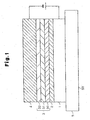
- Referring to Fig. 1, the organic EL device of the preferred embodiment includes a
transparent electrode 1. Thetransparent electrode 1 functions as an anode and is formed on a transparent substrate 5.Auxiliary electrodes 2 are formed on parts of thetransparent electrode 1. An organic layer 3 including an organic luminescent material is formed on thetransparent electrode 1 and theauxiliary electrodes 2. Anopposing electrode 4 functioning as a cathode is formed on the organic layer 3. The organic layer 3 emits light when current flows between thetransparent electrode 1 and theopposing electrode 4. The emitted light exits the organic EL device from alight exiting surface 50 defined on thetransparent electrode 1. Plasma treatment is performed on the portions of theauxiliary electrodes 2 that are not in contact with thetransparent electrode 1. - The
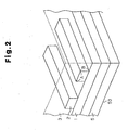
auxiliary electrodes 2 and thetransparent electrode 1 will now be discussed in detail. - Referring to Fig. 2, the
auxiliary electrodes 2 are formed on parts of the transparent electrode 1 (on the side of the organic layer 3, which is indicated by the broken lines). Eachauxiliary electrode 2, which is a conductive layer having a resistivity that is less than that of thetransparent electrode 1, is electrically connected to thetransparent electrode 1. The employment of theauxiliary electrodes 2 has the effects described below. - The arrangement of the low resistivity
auxiliary electrodes 2 on parts of thetransparent electrode 1, which functions as the anode, decreases resistance of the anode as a whole. - The potential becomes uniform throughout the entire surface of the
transparent electrode 1 when using theauxiliary electrodes 2. Thus, the amount of the generated light (luminance) becomes uniform. - The
auxiliary electrodes 2 may be made of any material enabling theauxiliary electrodes 2 to have resistivity that is less than that of thetransparent electrode 1. For example, the material may be selected from Al, Sc, Nb, Zr, Hf, Nd, Ta, Cu, Si, Cr, Mo, Mn, Ni, Pd, Pt, and W. Theauxiliary electrodes 2 may be made of only one of these materials or an alloy obtained by mixing two or more of these materials. When using two or more of these materials, the materials may be mixed at any mixing ratio. Excluding inevitable components that become mixed with the material or become included during manufacturing, it is preferred that the metal elements of these materials be the elements that essentially form theauxiliary electrodes 2. - Among the above materials, it is preferred that the
auxiliary electrodes 2 be formed of only Al or an alloy including Al as the main component and one or more of the above transition elements. It is preferable that the content of Al in the alloy be 90at% or more, and more preferably, 95at% or more. - The line width A of the
auxiliary electrodes 2 on thetransparent electrode 1 is not restricted. - It is preferred that the thickness B of the
auxiliary electrodes 2 be less than the thickness of the organic layer 3. The thickness B of theauxiliary electrodes 2 is preferably 10 to 1000 nm, more preferably 20 to 500 nm, and most preferably 100 to 300 nm. When the light emitted from the organic layer 3 exits thetransparent electrode 1, theauxiliary electrodes 2 may be transparent. In this case, it is preferred that the transmittance of the light emitted from the organic layer 3 be 80% or more. For example, when theauxiliary electrodes 2 are formed from Pt, the transmittance of visible light is approximately 82% when the thickness B is 1 nm. Thus, the thickness B is preferably 0.5 to 20 nm, and more preferably 1 to 10 nm. - Plasma treatment is performed on the surfaces of each
auxiliary electrode 2 that do not contact thetransparent electrode 1. The surfaces of theauxiliary electrode 2 need only be substantially plasma-treated and do not have to be completely plasma-treated. For example, plasma treatment of only the surface of theauxiliary electrode 2 facing away from thetransparent electrode 1 or the surface contacting the organic layer 3 would be sufficient. Plasma treatment is performed on 50% or more of the portions of theauxiliary electrode 2 that are free from thetransparent electrode 1, more preferably, 75% or more of the portions of theauxiliary electrode 2 that are free from thetransparent electrode 1, and most preferably, 90% or more of the portions of theauxiliary electrode 2 that are free from thetransparent electrode 1. - Known plasma treatments used to treat surfaces of electrodes, such as DC plasma treatment or RF plasma treatment, are employed as the plasma treatment.
- Gas is used during the plasma treatment. Any gas may be employed as the treatment gas. For example, inert gas such as argon (Ar) may be used. Alternatively, gases such as oxygen (O) or nitrogen (N) may be used.
- When using gas including oxygen for plasma treatment, the surface of the
auxiliary electrode 2 free from thetransparent electrode 1 is partially or completely oxidized. This hinders or completely stops the flow of current from theauxiliary electrode 2 to the organic layer 3. Especially, when theauxiliary electrode 2 is not transparent, most of the light emitted from the organic layer 3 at the rear side of theauxiliary electrode 2 would be blocked by theauxiliary electrode 2 and cannot be emitted out of the device. If there were to be no emission of light at such region of the organic layer 3 located at the rear side of theauxiliary electrode 2, this would reduce power consumption without affecting the amount of light exiting the device (i.e., the amount of usable light). Thus, the surfaces of theauxiliary electrode 2 that are free from thetransparent electrode 1 may be insulative or have a resistance that is greater than that in the interior of theauxiliary electrode 2. - The flow rate of the treatment gas differs depending on the operation conditions or the type of the used gas. However, the flow rate is normally 5 to 500 SCCM in O2 conversion. It is preferred that the operation pressure normally be approximately 0.3 to 5 Pa.
- Normally, high frequency power having a high frequency of approximately 13.56 MHz and a power of approximately 0.1 to 5 kW is applied to a high frequency induction coil used for plasma treatment. However, this is only one example and the applied frequency and power may be of any value as long as it enables plasma to be generated and maintained.
- The time of plasma treatment is preferably one minute or longer and more preferably two to twenty minutes.
- The plasma treatment of the surfaces of the
auxiliary electrode 2 in this manner substantially eliminates the occurrence of bright spots around theauxiliary electrode 2. Further, the luminance difference in thelight exiting surface 50 between positions around eachauxiliary electrode 2 and other positions is minimized. - Accordingly, the organic EL device of the preferred embodiment does not have luminance differences. It is believed that this is because the plasma treatment on the surfaces of each
auxiliary electrode 2 smoothes the surfaces and eliminates portions where theauxiliary electrode 2 contacts the opposingelectrode 4 or is located closely to the opposingelectrode 4. - In the prior art, bright spots are produced, and portions brighter than other portions are produced. It is believed that this occurs due to land and pits formed in each
auxiliary electrode 2. The lands and pits result in portions at which the distance between theauxiliary electrode 2 and the opposingelectrode 4 becomes extremely short. This causes the thickness of the organic layer 3 arranged between theauxiliary electrode 2 and the opposingelectrode 4 at such portions to be thinner than other portions. The resistance at thin portions of the organic layer 3 is lower than other portions. Thus, more current flows at the thin portions and increases the luminance of the thin portions. Further, the temperature is higher at portions where more current flows. This further decreases the resistance and increases the luminance. Accordingly, this would produce bright spots near theauxiliary electrode 2 in thelight exiting surface 50, and the luminance at such portions would be higher than other portions. - However, in the organic EL device of the preferred embodiment, the
auxiliary electrode 2 is smoothed. Thus, a sufficient distance is provided between theauxiliary electrode 2 and the opposingelectrode 4. In other words, the thickness of the organic layer 3 between theauxiliary electrode 2 and the opposingelectrode 4 is sufficient in comparison to other positions. This prevents the luminance from increasing and bright spots from being produced. As a result, luminance differences are substantially eliminated. Further, this prolongs the life of the elements at such portions. This, in turn, prolongs the life of the organic EL device. - It has been confirmed that there are substantially no bright spots or luminance differences when the surface roughness of the
auxiliary electrode 2 is as described below. - (1) The surface of the
auxiliary electrode 2 is smoothed to 80 nm or less under the ten point height of roughness profile standard, which is defined by the Japanese Industrial Standard (JIS) B0601 2001. The ten point height of roughness profile is obtained from a roughness profile of a predetermined sampling length. The mean of the heights of the highest peak to the fifth highest peak in the roughness profile is added to the mean of the depths of the lowest valley to the fifth lowest valley in the roughness profile. The sum of the means is referred to as the ten point height of roughness. - (2) The
auxiliary electrode 2 is smoothed so that its surface roughness under the ten point height of roughness profile standard is less than or equal to the thickness of the organic layer 3. -
- In the above conditions, there is no lower limit to the ten point height of roughness profile standard. However, satisfactory results were obtained when the surface roughness of the
auxiliary electrode 2 was approximately 20 nm. - The smoothing of the
auxiliary electrode 2 in this manner eliminates leakage from between theauxiliary electrode 2 and the opposingelectrode 4 and eliminates extremely thin portions from the organic layer 3. - When designing the surface of the
auxiliary electrode 2 so that the ten point height of roughness profile standard satisfies the above condition after the arithmetical mean deviation of the surface becomes 0.1 nm or greater and 5.0 nm or less, the results are especially satisfactory. The arithmetical mean deviation is defined by JIS B0602 2001. - When the surface roughness under the ten point height of roughness profile standard of the
auxiliary electrode 2 is 1/1.6 or less of the thickness of the organic layer 3, the resulting organic EL device has minimized luminance differences and the possibility of bright spots being produced is extremely small. - The
auxiliary electrodes 2 are formed on thetransparent electrode 1 using known film formation processes, such as plasma chemical vapor deposition (CVD), sputtering, vacuum vapor deposition, and EB vapor deposition. It is especially preferred that vacuum vapor deposition be performed to form theauxiliary electrodes 2 from the same material as that of the cathode so that the electrodes may be formed in the same vacuum vapor deposition device. - The employment of sputtering increases adhesion between the
transparent electrode 1 and theauxiliary electrodes 2. - When performing sputtering, the target that is used has the same composition as the auxiliary electrodes 2 (sinter formed from the above metals or alloy). The
auxiliary electrodes 2 that are formed have substantially the same composition as the target. - It is preferred that the pressure of sputtering gas during sputtering be in the range of 0.5 to 5 Pa. A hole injection layer having a concentration gradient may easily be obtained by varying the pressure of the sputtering gas in the above range when performing sputtering.
- An inert gas that is used in a typical sputtering device may be used. Among such gases, it is preferred that one of Ar, Kr, and Xe or a gas mixture including at least one of these substances be used.
- Further, reactive sputtering using a reactive gas may also be performed. When forming an oxide, gases such as O2 and CO may be used as the reactive gas. When forming a nitride, gases N2, NH3, NO, NO2, and N2O may be used as the reactive gas. When forming a carbide, gases such as CH4, C2H2, C2H4, and CO may be used as the reactive gas. These reactive gases may be used solely or in combination with other gases.
- The sputtering may be DC sputtering or high frequency sputtering, which uses an RF power supply. However, RF sputtering is more preferable. The preferred film-forming rate is 0.5 to 10 nm/min.
- A know pattering process may be used to form the
auxiliary electrodes 2 with a predetermined shape on thetransparent electrode 1. For example, a patterning process using a resist that is normally used may be performed. In this case, dry etching or wet etching may be performed. When performing wet etching, it is preferred that the etching liquid used for wet etching be one selected in accordance with each metal. For example, when forming theauxiliary electrode 2 from Al, a mixture solution of phosphoric acid, nitric acid, and acetic acid may be used. - A barrier layer formed from titanium nitride or the like may be arranged between the
auxiliary electrode 2 and thetransparent electrode 1. It is preferred that the barrier layer has a sufficient etching characteristic with respect to the etchant of theauxiliary electrode 2. The preferred material of the barrier layer is chromium; a nitride, such as titanium nitride, molybdenum nitride, tantalum nitride, and chromium nitride; a silicide, such as cobalt silicide, chromium silicide, molybdenum silicide, tungsten nitride, and titanium silicide; titanium carbide; and doped silicon carbide. Among these substances, titanium nitride and chromium are preferable since they have superior anti-corrosion characteristics. The nitriding rate of titanium nitride is 5 to 55%. - The thickness of the barrier layer is preferably 5 to 200 nm, and more preferably, 30 to 100 nm.
- The
transparent electrode 1 is an electrode arranged on the light-exiting side of the organic layer 3. In the preferred embodiment, thetransparent electrode 1 functions as an anode arranged on the transparent substrate 5. - It is preferred that the material forming the
transparent electrode 1 be one that enables efficient injection of positive holes in the organic layer 3 (which includes a positive hole injection layer and a positive hole injection transportation layer). The preferred material is normally a substance having a work function of 4.5 to 5.5 eV. More specifically, the preferred material is one of which main composition is indium-tin-oxide (ITO), indium-zinc-oxide (IZO), indium oxide (In2O3), tin oxide (SnO2), and zinc oxide (ZnO). - These oxides may be slightly biased from the stoichiometric composition. The mixing ratio of SnO2 relative to In2O3 in ITO is 1 to 20 wt% and more preferably 5 to 12 wt%. The mixing ratio of ZnO relative to In2O3 in IZO is approximately 12 to 32 wt%. If the average value of the composition in the entire
transparent electrode 1 falls in this range, there may be a concentration gradation in the direction perpendicular to the plane of thetransparent electrode 1. - Additionally, substances, such as Sn, Ti, and Pb, may be included in the form of oxides at 1 wt% or less in oxide conversion.
- In this specification, the term "transparent" refers to the light transmittance, in which light exiting from the device, is 50% or greater, preferably 80% or greater, and more preferably 90% or greater. Normally, light having a wavelength of 400 to 800 nm (visible light) is emitted out of the device. When the transmittance becomes too low, the light emission from the luminescent layer is attenuated. This makes it difficult to obtain the necessary luminance from the luminescent device.
- The thickness of the
transparent electrode 1 is required only to enable sufficient injections of positive holes in the organic layer 3. The preferred thickness of thetransparent electrode 1 is normally 10 to 50 nm. Although there is no limit to the upper limit of the thickness, when thetransparent electrode 1 is too thick, the transmittance may decrease or exfoliation of thetransparent electrode 1 may occur. If thetransparent electrode 1 is too thin, the injection of positive holes may be disabled and the film strength may be insufficient when manufacturing the device. It is necessary that the drive voltage be low to increase the reliability of the device. The preferred electrode is a sheet of ITO having a resistance of 3 to 30 Ω and a thickness of 50 to 300 nm. For actual usage, the thickness or optical constant of the electrode may be set so that the buffering effect resulting from reflection at the hole injection electrode interface of ITO or the like sufficiently satisfies the required light exiting efficiency or the color purity. - The
transparent electrode 1 may be formed through a known film formation process such as vapor deposition. However, it is preferred that thetransparent electrode 1 be performed through sputtering. When performing sputtering to form an ITO or IZO electrode, it is preferred that a target in which SnO2 or ZnO is doped in In2O3 be used. When forming an ITO transparent electrode through sputtering, moment-to moment change in the luminance of the emitted light is small in comparison to when forming an electrode through vapor deposition. The preferred sputtering is DC sputtering or RF sputtering, the power that is used is preferably in the range of 0.1 to 4 W/cm2. The film forming rate is 2 to 100 nm/min, and more preferably 5 to 50 nm/min. The sputtering gas is not limited and an inert gas, such as Ar, He, Ne, Kr, and Xe, or a mixture of these gases may be used. The pressure of the sputtering gas during sputtering is normally about 0.1 to 20 Pa. - Further, in the same manner as the
auxiliary electrodes 2, plasma treatment may be performed on thetransparent electrode 1. When performing the plasma treatment, thetransparent electrode 1 and theauxiliary electrodes 2 may be treated together (simultaneously) or separately. - The organic layer 3 and the opposing
electrode 4 will now be described. - The organic layer 3 includes an organic luminescent material such as Alq3 or DCM. The organic layer 3, of which the main composition is an organic material, emits electroluminescence when voltage is applied between the
transparent electrode 1 and the opposingelectrode 4. - The organic layer 3 includes one layer or a plurality of superimposed layers. When the organic layer 3 has a superimposed structure, layers including the organic luminescent material are referred to as luminescent layers.
- Referring to Fig. 1, the
transparent electrode 1, which functions as an anode, is formed on the substrate 5. Theauxiliary electrodes 2 are formed on thetransparent electrode 1. A holeinjection transport layer 30, a luminescent layer 31, and an electroninjection transport layer 32 are formed on thetransparent electrode 1 and theauxiliary electrode 2 on the side facing away from the transparent substrate 5. The holeinjection transport layer 30, the luminescent layer 31, and the electroninjection transport layer 32 form the organic layer 3. However, the organic layer 3 is not limited to such structure and may have other structures. - For example, the hole
injection transport layer 30 may be eliminated by providing the luminescent layer with the functions of the hole injection transport layer, that is, a hole injection function and a hole import function. Alternatively, the electroninjection transport layer 32 may be separated into an electron injection layer provided with an electron injection function and an electron transport layer provided with the electron injection function. In this case, the electron injection layer and the electron transport layer are superimposed with each other. Examples of other alternatives of the structure of the organic layer 3 are listed below.
(Anode) / hole injection layer / hole transport layer / luminescent layer / non-luminescent layer / electron transport layer / electron injection layer / (cathode)
(Anode) / hole injection layer / hole transport layer / luminescent layer / non-luminescent layer / electron injection transport layer / (cathode)
(Anode) / hole injection transport layer / luminescent layer / non-luminescent layer / electron transport layer / electron injection layer / (cathode.)
(Anode) / hole injection transport layer / luminescent layer / non-luminescent layer / electron injection transport layer / (cathode)
(Anode) / luminescent layer / non-luminescent layer / electron transport layer / electron injection layer / (cathode)
(Anode) / luminescent layer / non-luminescent layer / electron injection transport layer / (cathode) - Each of the above layers may be provided with various functions. For example, the luminescent layer may be provided with a hole transport function, a hole injection function, an electron injection function, and/or an electron transport function.
- Layers that are not described above may also be included. The layers may also be superimposed in a substrate starting from the cathode to form the organic EL device.
- The hole
injection transport layer 30, into which holes are injected from thetransparent electrode 1 and which transports the injected holes to the luminescent layer 31, is arranged between thetransparent electrode 1 and the luminescent layer 31. Ionization energy of the holeinjection transport layer 30, which is set to be between the work function of thetransparent electrode 1 and the ionization energy of the luminescent layer 31, is usually set at 5.0 to 5.5 eV. - The organic EL device of Fig. 1 that includes the hole
injection transport layer 30 has the following properties. - (1) Driving voltage is low.
- (2) Injection of holes into the luminescent layer 31 from the transparent electrode is stabilized. This prolongs the life of the device.
- (3) Adhesion between the opposing
electrode 4, which functions as the cathode, and the luminescent layer 31 increases. This increases the uniformity of the luminescent surface. - (4) The coating of the protrusions on the surface of the anode reduces device deficiencies.
-
- When the light emitted by the luminescent layer 31 is output through the hole
injection transport layer 30, the holeinjection transport layer 30 is transparent. Among the materials that can form the holeinjection transport layer 30, the material is selected from one that transmits the emitted light when formed into a thin film. In general, the transmittance of the holeinjection transport layer 30 with respect to the emitted light is greater than 10%. - The material for forming the hole
injection transport layer 30 is not especially limited as long as the above-described properties are imparted to the holeinjection transport layer 30. Any known material used as a hole injection material of a photoconductive device or any known material used for a hole injection transport layer in an organic EL device may be used. - Examples of the material for forming the hole
injection transport layer 30 include phthalocyanine derivatives, triazole derivatives, triarylmethane derivatives, triarylamine derivatives, oxazole derivatives, oxadiazole derivatives, hydrazone derivatives, stilbene derivatives, pyrazoline derivatives, pyrazolone derivatives, polysilane derivatives, imidazole derivatives, phenylenediamine derivatives, amino substituted chalcone derivatives, styrylanthracene derivatives, fluorenone derivatives, hydrazone derivatives, silazane derivatives, aniline copolymer, porphyrin compounds, polyarylalkane derivatives, polyphenylene vinylene and derivatives thereof, polythiophene and derivatives thereof, poly-N-vinylcarbazole derivatives, electroconductive polymeric oligomers such as thiophene oligomer, metallophthalocyanines such as copper phthalocyanine, and tetra(t-butyl)copper phthalocyanine, metal-free phthalocyanines, quinacridone compounds, aromatic tertiary amine compounds, and styrylamine compounds. - Examples of the triarylamine derivatives include 4,4'-bis[N-phenyl-N-(4"-methylphenyl)amino]biphenyl, 4,4'-bis [N-phenyl-N-(3"-methylphenyl)amino] biphenyl, 4,4'-bis[N-phenyl-N-(3"-methoxyphenyl)amino]biphenyl, 4,4'-bis[N-phenyl-N-(1"-naphththyl)amino]biphenyl, 3,3'-dimethyl-4,4'-bis[N-phenyl-N-(3"-methylphenyl)amino]biphenyl, 1,1-bis[4'-[N,N-di(4"-methylphenyl)amino]phenyl]cyclohexane, 9,10-bis[N-(4'-methylphenyl)-N-(4"-n-butylphenyl)amino]phenanthrene, 3,8-bis(N,N-diphenylamino)-6-phenanthridine, 4-methyl-N,N-bis[4",4"'-bis[N',N"-di(4-methylphenyl)amino]biphenyl-4-yl]aniline, N,N''-bis[4-(diphenylamino)phenyl]-N,N'-diphenyl-1,3-diaminobenzene, N,N'-bis[4-(diphenylamino)phenyl]-N,N'-diphenyl-1,4-diaminobenzene, 5,5"-bis [4-(bis[4-methylphenyl] amino)phenyl]-2,2':5',2"-terthiophen, 1,3,5-tris(diphenylamino)benzene, 4,4',4"-tris(N-carbazolyl)triphenylamine, 4,4',4"-tris[N-(3'''-methylphenyl)-N-phenylamino]triphenylamine, 4,4',4"-tris[N,N-bis(4'''-tert-butylbiphenyl-4""-yl)amino]triphenylamine, and 1,3,5-tris[N-(4'-diphenylaminophenyl)-N-phenylamino]benzene.
- Examples of the porphyrin compounds include porphin, 1,10,15,20-tetraphenyl-21H,23H-porphin copper (II), 1,10,15,20-tetraphenyl-21H,23H-porphin zinc (II), 5,10,15,20-tetrakis (pentafluorophenyl)-21H,23H-porphin, silicon phthalocyanine oxide, aluminum phthalocyanine chloride, phthalocyanine (metal-free), dilithium phthalocyanine, copper tetramethyl phthalocyanine, copper phthalocyanine, chromium phthalocyanine, zinc phthalocyanine, lead phthalocyanine, titanium phthalocyanine oxide, magnesium phthalocyanine, and copper octamethyl phthalocyanine.
- Examples of the aromatic tertiary amine compounds and the styrylamine compounds include N,N,N',N'-tetraphenyl-4,4'-diaminophenyl, N,N'-diphenyl-N,N'-bis-(3-methylphenyl)-[1,1'-biphenyl]-4,4'-diamine, 2,2-bis(4-di-p-tolylaminophenyl) propane, 1,1-bis(4-di-p-tolylaminophenyl)cyclohexane, N,N,N',N'-tetra-p-tolyl-4,4'-diaminophenyl, 1,1-bis(4-di-p-tolylaminophenyl)-4-phenylcyclohexane, bis(4-dimethylamino-2-methylphenyl)phenylmethane, bis(4-di-p-tolylaminophenyl)phenylmethane, N,N'-diphenyl-N,N'-di(4-methoxyphenyl)-4,4'-diaminobiphenyl, N,N,N',N'-tetraphenyl-4,4'-diaminophenyl ether, 4,4'-bis(diphenylamino)quadriphenyl, N,N,N-tri(p-tolyl)amine, 4-(di-p-tolylamino)-4'-[4(di-p-tolylamino)styryl]stilbene, 4-N,N-diphenylamino-(2-diphenylvinyl)benzene, 3-methoxy-4'-N,N-diphenylamino stilbenzene, and N-phenylcarbazole. Further, aromatic dimethylidene compounds may be used as the materials of the hole
injection transport layer 30. - The hole
injection transport layer 30 may be formed from one of the above materials or from a mixture of a plurality of the above materials. Further, the holeinjection transport layer 30 may have a multi-layered structure including multiple layers having the same composition or different compositions. - The hole
injection transport layer 30 may be formed on the anode using a known thin film formation process, such as a vacuum vapor deposition, spin coating, casting, or LB process. The layer thickness is normally 5 nm to 5 µm, although it depends on the selected material. - The luminescent layer 31 is mainly formed from an organic material. The luminescent layer 31 has holes and electrons injected from the
transparent electrode 1 and the opposingelectrode 4, transports at least either the holes or the electrons, recombines the holes and the electrons to generate excitons, and emits electroluminescence (light) when the excitons return to a ground state. - Therefore, the material (organic material) of the luminescent layer 31 is only required to have the following functions:
- hole injection function allowing injection of holes from the hole injection transport layer 30 (or transparent electrode 1);
- electron injection function allowing injection of
electrons from the electron
injection transport layer 32; - transport function for transporting at least either the injected holes or electrons with the force of an electric field;
- function for recombining the holes and the electrons to produce an excited state (excitons); and
- function for generating electroluminescence when transition from the excited state to the ground state occurs.
-
- Typical examples of having the above functions include Alq3 and Be benzoquinolinol (BeBq2). Further, the following materials may also be used.
- Benzoxazole materials such as 2,5-bis(5,7-di-tert-pentyl-2-benzoxazolyl)-1,3,4-thiadiazole, 4,4'-bis(5,7-pentyl-2-benzoxazolyl)stilbene, 4,4'-bis[5,7-di-(2-methyl-2-butyl)-2-benzoxazolyl]stilbene, 2,5-bis(5,7-di-tert-pentyl-2-benzoxazolyl)thiophine, 2,5-bis([5-α,α-dimethylbenzyl]-2-benzoxazolyl)thiophene, 2,5-bis[5,7-di-(2-methyl-2-butyl)-2-benzoxazolyl]-3,4-diphenylthiophene, 2,5-bis(5-methyl-2-benzoxazolyl)thiophene, and 4,4'-bis(2-benzoxazolyl)biphenyl, 5-methyl-2-[2-[4-(5-methyl-2-benzoxazolyl)phenyl]vinyl]benzoxazolyl, 2-[2-(4-chlorophenyl)vinyl]naphth[1,2-d]oxazole; benzothiazole materials such as 2,2'-(p-phenylene divinylene)-bis benzothiazole; benzimidazole fluorescent whitening agents such as 2-[2-[4-(2-benzimidazolyl)phenyl]vinyl]benzimidazole, and 2-[2-(4-carboxyphenyl)vinyl]benzimidazole; 8-hydroxyquinoline metallic complexes such as bis(8-quinolinol)magnesium, bis(benzo-8-quinolinol)zinc, bis(2-methyl-8-quinolinolate) aluminium oxide, tris(8-quinolinol)indium, t ris(5-methyl-8-quinolinol)aluminium, 8-quinolinol lithium, tris (5-chloro-8-quinolinol) gallium, bis(5-chloro-8-quinolinol) calcium, and poly[zinc-bis(8-hydroxy-5-quinolinonyl)methane]; metal chelated oxynoid compounds such as dilithium epindrydione; styryl benzene compounds such as 1,4-bis(2-methylstyryl)benzene, 1,4-(3-methylstyryl)benzene, 1,4-bis(4-methylstyryl)benzene, distyrylbenzene, 1,4-bis(2-ethylstyryl) benzene, 1,4-bis(3-ethylstyryl) benzene, and 1,4-bis(2-methylstyryl)2-methylbenzene; distyryl pyrazine derivatives such as 2,5-bis (4-methylstyryl)pyrazine, 2,5-bis(4-ethylstyryl)pyrazine, 2,5-bis[2-(1-naphthyl)vinyl]pyrazine, 2,5-bis(4-methoxystyryl)pyrazine, 2,5-bis[2-(4-biphenyl)vinyl]pyrazine, and 2,5-bis[2-(1-pyrenyl)vinyl]pyrazine; naphthalimide derivatives; perylene derivatives; oxadiazole derivatives; aldazine derivatives; cyclopentanediene derivatives; styrylamine derivatives; cumarin derivatives; aromatic dimethylidine derivatives; anthracene; salicylate; pyrene; coronene and, phosphorescent materials, such as fac-tris(2-phenylpyridine)iridium.
- Further, the luminescent layer 31 may contain a material (organic luminescent material/dopant) having a function for generating electroluminescence and a material (host material) having other functions. In this case, the host material injects and transports carriers and is raised to an excited state by recombination. The excited host material transfers excitation energy to the dopant. The dopant generates electroluminescence when returning to the ground state. In general, a fluorescent material or a phosphorescent material is used as the dopant.
- The host material is only required to have the above functions and known materials may be used as the host material. Examples of the host material include distyrylallylene derivatives, distyrylbenzene derivatives, distyrylamine derivatives, quinolinolate metallic complexes, triarylamine derivatives, azomethine derivatives, oxadiazole derivatives, pyrazoloquinoline derivatives, silole derivatives, naphthalene derivatives, anthracene derivatives, dicarbazole derivatives, perylene derivatives, oligothiophene derivatives, cumarin derivatives, pyrene derivatives, tetraphenylbutadiene derivatives, benzopyrane derivatives, europium complexes, rubrene derivatives, quinacridone derivatives, triazole derivatives, benzoxazole derivatives, and benzothiazole derivatives.
- The fluorescent material is a material, such as a fluorochrome or a fluorescent dopant, capable of emitting light during transition to the ground state after receiving excitation energy from the host material. This enables the exit of light from the singlet state of excitation under normal temperatures. In general, a material having a high quantum efficiency of fluorescence is selected as the fluorescent material. The amount of fluorescent material to be doped to the host material is 0.01 wt% or more to 20 wt% or less with respect to the host material.
- The fluorescent material is only required to be selected from known materials having the above properties. Examples of the fluorescent material include europium complexes, benzopyrane derivatives, rhodamine derivatives, benzothioxanthen derivatives, porphyrin derivatives, Nile red, 2-(1,1-dimethylethyl)-6-(2-(2,3,6,7-tetrahydro-1,1,7,7-tetramethyl-1H, 5H-benzo(ij)quinolidin-9-yl)ethenyl)-4H-pyrane-4H-ylidene)propanedinitrile (DCJTB), DCM, cumarin derivatives, quinacridone derivatives, distyrylamine derivatives, pyrene derivatives, perylene derivatives, anthracene derivatives, benzoxazole derivatives, benzothiazole derivatives, benzimidazole derivatives, chrysene derivatives, phenanthrene derivatives, distyrylbenzene derivatives, tetraphenylbutadiene, and rubrene.
- The phosphorescent material is a material, such as a phosphorescent dye or a phosphorescent dopant, capable of emitting light during transition to the ground state after receiving excitation energy from the host material. This enables the exit of light from the singlet and triplet states under normal temperatures. In general, the amount of phosphorescent material to be doped to the host material is 0.01 wt% or more to 30 wt% or less with respect to the host material.
- The phosphorescent material is not limited as long as it enables usage of light emission from the singlet and triplet states of excitation under normal room temperatures. A known phosphorescent material may be used as the phosphorescent material. In general, heavy metal complexes capable of emitting phosphorescent light are used as the phosphorescent material.
- For example, tris(2-phenylpyridine)iridium may be used as a green phosphorescent material. Further, 2,3,7,8,12,13,17,18-octaethyl-21H23H-porphinplatinum(II) may be used as a red phosphorescent material. Other metals or nonmetals may be substituted for the central metals of the above materials.
- The luminescent layer 31 may be formed on the hole
injection transport layer 30 with a known thin film formation process, such as the vacuum vapor deposition, spin coating, casting, or LB process. The layer thickness of the luminescent layer 31 is generally about 1 nm to 100 nm, and preferably about 20 nm to 50 nm, although it depends on the used material. - Further, if the same layer is doped with a plurality of dopants, it becomes possible to mix colors of emitted light, emit two or more light colors, and efficiently transfer the energy to a second dopant having a lower energy level after transferring energy from the host material to a first dopant having a low energy level.
- The chromaticity, saturation, brightness, and luminance of light (electroluminescence) emitted from the luminescent layer 12 are adjusted by selecting the kind of material of the luminescent layer 31, adjusting the amount of the dopant that is doped, and adjusting the thickness of the luminescent layer 31. It is also possible to adjust the luminescent color of light emitted from the luminescent layer 31 through the processes described below. The luminescent color may be adjusted by using one of these processes or by using more than one of these processes.
- Process for adjusting the luminescent color by arranging a color filter on the light exiting side of the luminescent layer 31
- The color filter adjusts the luminescent color by limiting the wavelength range of light transmitted through the filter. Color filters are made by using known materials. For example, a blue filter is made of cobalt oxide, a green filter is made of a mixture of cobalt oxide and chromium oxide, and a red filter is made of ferrous oxide. The color filter may be formed on the substrate 5 by using a known thin film formation process, such as vacuum vapor deposition.
- Process for adjusting the luminescent color by doping materials for enhancing or inhibiting luminescence
- For example, the luminescent layer 31 is doped with a so-called assist dopant, which receives energy from the host material and transfers the energy to the dopant. This facilitates energy transfer from the host material to the dopant. The assist dopant is selected from known materials, such as the materials used as the above host materials and dopants.
- Process of adjusting the luminescent color by doping a layer (including the substrate 5) at the light exiting side of the luminescent layer 31 with a material for changing the wavelengths of the emitted light
- A known wavelength converting material may be used as this material. For example, the material that is used may be a fluorescence conversion substance that converts light emitted from the luminescent layer 31 to another light having low energy wavelengths. The fluorescence conversion substance is selected as required in accordance with the wavelengths of light emitted from the organic EL device and the wavelengths of light emitted from the luminescent layer 31. Further, although the amount of the fluorescence conversion substance used may be selected as required depending on the kind of fluorescence conversion substance as long as it does not cause concentration quenching. Approximately 10-5 to 10-4 mol/liter is suitable with respect to a transparent (uncured) resin. It is possible to use only one type of a fluorescence conversion substance or plural types of fluorescence conversion substances. When plural types of fluorescence conversion substances are used, in addition to blue light, green light, and red light, white light and light having an intermediate color may be emitted depending on the combination of the substances. As the above fluorescence conversion substances, materials described in the following paragraphs (a) to (c) may be used.
- (a) Fluorescence conversion substances which emit blue
light when excited by ultraviolet rays
stilbene dyes, such as 1,4-bis(2-methylstyrene)benzene and trans-4,4'-diphenylstilbene; coumarin-based dyes, such as 7-hydroxy-4-methylcoumarin; and aromatic dimethylidene-based dyes, such as 4,4'-bis(2,2-diphenylvinyl)biphenyl. - (b) Fluorescence conversion substances which emit green
light when excited by blue light
coumarin dyes, such as 2,3,5,6-1H,4H-tetrahydro-8-trifluoromethylquinolizino(9,9a,1-gh)coumarin (coumarin 153). - (c) Fluorescence conversion substances which emit light
having wavelengths of orange to red when excited by light
having wavelengths of blue to green
cyanine dyes, such as 4-(dicyanomethylene)-2-methyl-6-(p-dimethylaminostyrylryl)-4H-pyrane, 4-(dicyanomethylene)-2-phenyl-6-(2-(9-julolidyl)ethenyl)-4H-pyrane, 4-(dicyanomethylene)-2,6-di(2-(9-julolidyl)ethenyl)-4H-pyrane, 4-(dicyanomethylene)-2-methyl-6-(2-(9-julolidyl)ethenyl)-4H-pyrane, and 4-(dicyanomethylene)-2-methyl-6-(2-(9-julolidyl)ethenyl)-4H-thiopyrane; pyridine dyes such as 1-ethyl-2-(4-(p-dimethylaminophenyl)-1,3-butadienyl)-pyridium-percolate (pyridine 1); xanthine dyes, such as rhodamine B and rhodamine 6G; and oxazine dyes. -
- The electron
injection transport layer 32 is arranged between theopposed electrode 4 and the luminescent layer 31 to transport the electrons injected from theopposed electrode 4 to the luminescent layer 31 and provides the organic EL device with the properties described below: - (1) Decrease driving voltage.
- (2) Stabilize injection of holes into the luminescent
layer 31 from the opposing
electrode 4. This prolongs the life of the device. - (3) Increase adhesion between the opposing
electrode 4, which functions as the cathode, and the luminescent layer 31. This increases the uniformity of the luminescent surface. - (4) Coating the protrusions on the surface of the anode to reduce device deficiencies.
-
- The material for the electron
injection transport layer 32 is selected from known materials used as electron injection materials for photoconductive materials and known materials used for forming electron injection transport layers in organic EL devices. In general, material having electron affinity between the work function of the cathode and the electron affinity of the luminescent layer 31 is used. - Specific examples of such materials include 1,3-bis[5'-(p-tert-butylphenyl)-1,3,4-oxadiazol-2'-yl]benzene and 2-(4-biphinylyl)-5-(4-tert-butylphenyl)-1,3,4-oxadiazole; and triazole derivatives such as 3-(4'-tert-butylphenyl)-4-phenyl-5-(4"-biphenyl)-1,2,4-triazole. Further, triazine derivatives, perylene derivatives, quinoline derivatives, quinoxaline derivatives, diphenylquinone derivatives, nitration fluorenone derivatives, thiopyranedioxide derivatives, anthraquinodimethane derivatives, thiopyranedioxide derivatives, heterocycle tetracarboxylic acid anhydrides such as naphthaleneperylene, carbodiimide, fluorenylidenemethane derivatives, anthraquinodimethane derivatives, anthron derivatives, and distyryl pyrazine derivatives may be used.
- Organometal complexes, such as bis(10-benzo[h]quinolinolato)beryllium, a beryllium salt of 5-hydroxyflavone and an aluminum salt of 5-hydroxyflavone are preferably used. Metal complexes of 8-hydroxyquinoline or its derivatives are further preferably used. More specifically, it is possible to use metal chelate oxynoid compounds having oxine (also known as 8-quinolinol or 8-hydroxyquinoline) ligands, such as tris(8-quinolinolato) aluminum, tris (5, 7-dichloro-8-quinolinolato) aluminum, tris(5,7-dibromo-8-quinolinolato) aluminum, and tris(2-methyl-8-quinolinolato) aluminum may be used. It is also possible to use metal complexes formed by substituting indium, magnesium, copper, calcium, tin or lead for the central metals of the above metal complexes. Metal-free phthalocyanine, metal phthalocyanine, or compounds having terminals of these compounds substituted by an alkyl group or a sulfone group may also be used.
- The electron
injection transport layer 32 may be formed by only one of the above materials or by mixing a plurality of the above materials. Further, the electroninjection transport layer 32 may have a multi-layered structure including multiple layers having the same composition or different compositions. - The electron
injection transport layer 32 is formed by using one or more of the above materials by performing any one of the known thin film formation processes, such as the sputtering, ion plating, vacuum vapor deposition, spin coating, and electron beam vapor deposition processes. The thickness of the electroninjection transport layer 32 is normally 5 nm to 5 µm. - When the electron
injection transport layer 32 is arranged at the light exit side of the luminescent layer 31, the electroninjection transport layer 32 is required to be transparent with respect to the exiting light. Thus, a material that is transparent when formed into a thin film is selected from the above-mentioned materials capable of forming the electroninjection transport layer 32. In general, the transmittance of the electroninjection transport layer 32 with respect to exiting light is set to be greater than 10%. - The organic EL device of the preferred embodiment may be provided with a known layer other than the layers shown in Fig. 1. Further, the formed layers may be doped with a known dopant. For example, the variations described below are possible.
- Interlayer layers for enhancing electron injection and hole injection may be provided. For example, a cathode interface layer (mixed electrode), which is formed by co-depositing the materials of the opposing
electrode 4 and the electroninjection transport layer 32 may be interposed between the opposingelectrode 4 and the electroninjection transport layer 32. This makes it possible to alleviate an energy barrier blocking electron injection between the luminescent layer 31 and the opposingelectrode 4. It also enhances adhesion between the opposingelectrode 4 and the electroninjection transport layer 32. - The cathode interface layer may be formed by using any known material that imparts the above properties to the cathode interface layer. For example, it is possible to use alkali metals, such as lithium fluoride, lithium oxide, magnesium fluoride, calcium fluoride, strontium fluoride, and barium fluoride, and fluorides, oxides, chlorides, and sulfides of alkaline-earth metals. The cathode interface layer may be formed from only one of the above materials or from more than one of the above materials. The thickness of the cathode interface layer is about 0.1 nm to 10 nm, preferably 0.3 nm to 3 nm.
- The cathode interface layer may have a uniform thickness or a non-uniform thickness. Further, the cathode interface layer may have an island-like shape and may be formed employing a known thin film formation process, such as the vacuum vapor deposition process.
- In order to prevent the
organic EL device 100 from being brought into contact with oxygen and water, a protective layer (sealing layer, passivation film) may be provided. An organic polymer material, an inorganic material, and a photo-curing resin may be used as the material of the protective layer. When forming the protective layer, one or a plurality of these materials may be used. The protective layer may have a single-layered structure or a multi-layered structure. - Examples of the organic polymer material include chlorotrifluoroethylene polymer, dichlorodifluoroethylene polymer, fluorine resins such as a copolymer of chlorotrifluoroethylene polymer and dichlorodifluoroethylene polymer, acryl resin such as polymethyl methacrylate, and polyacrylate, epoxy resin, silicone resin, epoxy-silicone resin, polystyrene resin, polyester resin, polycarbonate resin, polyamide resin, polyimide resin, polyamide-imide resin, poly paraxylene resin, polyethylene resin, and polyphenylene oxide resin.
- As the inorganic material, a thin film of diamond, amorphous silica, electrical insulating glass, metal oxides, metal nitrides, metal carbides, and metal sulfides may be used.
- The above materials may be doped with the aforementioned fluorescence conversion substance. Further, the organic EL device may be protected by sealing the organic EL device in inert substances, such as paraffin, liquid paraffin, silicone oil, fluorocarbon oil, and zeolite-added fluorocarbon oil.
- The hole
injection transport layer 30 and the electroninjection transport layer 32 may be doped with organic luminescent materials (dopants), such as a fluorescent material and a phosphorescent material, so that light is also emitted from the hole electroninjection transport layer 30 and the electroninjection transport layer 32. - When the cathode 15 is formed using a metal, such as aluminum, a layer adjacent to the opposing
electrode 4 may be doped with an alkali metal or an alkali metal compound to alleviate an energy barrier existing between the opposingelectrode 4 and the organic luminescent layer 31. The organic layer is chemically reduced by the metal or the compound to generate anions. This increases electron injection and lowers the applied voltage. As the alkali metal compound, for example, oxides, fluorides, and chelated lithium compounds may be used. - The opposing
electrode 4, which cooperates with the transparent electrode 3 to hold the organic layer 3 in between, functions as a cathode for injecting electrons into the electroninjection transport layer 32. The opposingelectrode 4 is made of a metal, an alloy, an electroconductive compound, or a mixture of these substances that have a work function of, for example, less than 4.5 eV, normally 4.9 eV or less, and typically 3.7 eV or less to increase the electron injecting efficiency. For example, K, Li, Na, Mg, La, Ce, Ca, Sr, Ba, Al, Ag, in, Sn, Zn, Zr may be used. These elements may be used solely or, to increase stability, in a state included in a two component or three component alloy. Alloys such as Ag·Mg (Ag: 0.01 to 50 at%), Al·Li (Li: 0.01 to 12 at%), In·Mg (Mg: 50 to 80 at%), and Al·Ca (Ca: 0.01 to 20 at%) prevent the opposingelectrode 4 from being oxidized and are preferable for increasing adhesion to the organic layer 3 (electron injection transport layer 32). Further, it is preferable that an oxide of these materials or a lithium oxide be used. This surrounds theorganic layer 4 with the opposingelectrode 4, which is an oxide, and thetransparent electrode 2, which is an oxide such as ITO. This improves weather-resistance. Further, the materials used to form the anode may also be used. - When the opposing
electrode 4 is used as a reflective electrode, among the above materials, materials provided with a function that reflects light emitted externally are selected. Normally, metals, alloys, and metals alloys are selected. - The opposing
electrode 4 may have a multi-layer structure including a plurality of layers made of the same composition or different compositions. For example, to reduce the work function of the opposingelectrode 4, oxides, fluorides, metal, and compounds having a small work function are inserted in the interface between the opposingelectrode 4 and the electroninjection transport layer 32 to reduce the work function of the opposingelectrode 4. For example, the material of the opposingelectrode 4 may be aluminum, and lithium fluoride or lithium oxide is inserted in the interface. - The opposing
electrode 4 is formed through a known thin film formation process, such as sputtering, ion vacuum deposition, ion plating, and electronic beam evaporation processes. Depending on the electrode material, the thickness of the opposingelectrode 4 should enable sufficient injection of electrons into the organic layer 3 and be 0.1 nm or greater and preferably 1 nm or greater. Although there is no upper limit, the upper limit is normally about 5 nm to 1 µm, more preferably about 5 to 1000 nm, further preferably about 10 nm to 500 nm; and most preferably about 50 nm and 200 nm. The electric resistance of the opposingelectrode 4 is preferably less than or equal to several hundreds of mm ohms/sheet. - When performing vapor deposition to form the opposing electrode, the conditions for vacuum vapor deposition are not limited. It is however preferred that the degree of vacuum be 10-4 Pa or less and the vapor deposition rate be about 0.01 to 1 nm/sec.
- When the material forming the opposing
electrode 4 is the same as the material forming theauxiliary electrode 2, and the vapor deposition conditions, such as the vapor deposition rate, are set appropriately, the organic EL device may be formed using the same vacuum vapor deposition device. - When the opposing
electrode 4 and the protective electrode are formed through sputtering, the preferred pressure of the sputtering gas is in the range of 0.1 to 1 Pa. The sputtering gas is inert gas that is used in a normal sputtering device. - When forming the opposing
electrode 4 through sputtering, high frequency sputtering or DC sputtering may be performed. It is preferred that the power of the sputtering device be 1 to 10 W/cm2 for DC sputtering and 1 to 10 W/cm2 for RF sputtering. The film formation rate is preferably 5 to 100 nm/min, and more preferably 10 to 50 nm/min. - The opposing
electrode 4 is patterned by performing mask vapor deposition or by performing etching subsequent to the film formation. This separates devices and forms the desired luminescent pattern. - The substrate 5 is a plate-like member for supporting the organic EL device. The layers of the organic EL device are extremely thin and are thus usually supported by the substrate 5.
- The substrate 5 is the member on which the organic EL device is superimposed. It is thus preferable that the substrate has a smooth plane.
- When the substrate 5 is located on the light exiting side of the luminescent layer 31, the substrate 5 is transparent.
- As long as the substrate 5 has the above functions, any substrate may be used as the substrate 5. Examples of the substrate 5 include glass substrates, silicon substrates, ceramic substrates such as quarts substrates, and plastic substrates. Further, metals substrates or substrates to which a metal layer is applied to the supporting body may be used. A substrate formed by combining a plurality of the same or different substrates may also be used.
- As described above, the organic EL device of the preferred embodiment needs only to have the requirements listed below:
- (1) The organic layer 3 including an organic luminescent layer is held between a pair of electrodes.
- (2) At least one of the electrodes is transparent
(transparent electrode 1) and the other one of the
electrodes is the opposing
electrode 4. - (3) The light generated by the organic layer 3 is
emitted at least from the
transparent electrode 1. - (4) The
auxiliary electrode 2 of which resistivity is less than thetransparent electrode 1 is arranged between part of thetransparent electrode 1 and the organic layer 3. - (5) The surface of the
auxiliary electrode 2 that does not contact thetransparent electrode 1 or the surface that contacts the organic layer 3 is substantially smooth. -
- Accordingly, modifications as described below can be made.
- Known smoothing processes such as smoothing through polishing or smoothing through chemical processing may be performed. When employing such smoothing processes, the
transparent electrode 1 may be protected to smooth only theauxiliary electrode 2. Alternatively, thetransparent electrode 1 may be smoothed together with theauxiliary electrode 2. When performing smoothing in such a manner, the smoothing is performed to satisfy one of the conditions described below to provide an organic EL device having extremely small luminance differences. - Smooth the surface of the
auxiliary electrode 2 to 80 nm or less under the ten point height of roughness profile standard. Further, smooth the surface of theauxiliary electrode 2 so that the surface roughness under the ten point height of roughness profile standard is less than or equal to the thickness of the organic layer 3, and preferably 1/1.6 of the thickness of the organic layer 3. - As described above, the lower limit of the surface roughness of the
auxiliary electrode 2 under the ten point height of roughness profile standard is not limited. For example, an organic EL device having substantially no luminance differences may be formed even if the ten point height of roughness profile standard is in the range of 20 nm to 80 nm. - Further, when the surface of the
auxiliary electrode 2 is set as described above and smoothed to about 1.1 nm to 5.0 nm under the arithmetical mean deviation, a highly satisfactory organic EL device having no luminance differences is formed. - In addition to smoothing, the surface of the auxiliary electrode 2 (especially the surface contacting the organic layer 3) may be treated so that it is oxidized, so that it becomes insulative, or so that it has resistance that is greater than other parts of the
auxiliary electrode 2 to decrease power consumption without decreasing the amount of light emitted from the device in comparison to when such treatment is not performed. - The
auxiliary electrode 2 may also be transparent. Further, to obtain the necessary luminance, the arrangement of theauxiliary electrode 2 on thetransparent electrode 1 may be adjusted and the proportion of thetransparent electrode 1 occupied by theauxiliary electrode 2 may be changed to obtain sufficient luminance. - The
transparent electrode 1 may be used as the cathode, and the opposingelectrode 4 may be used as the anode. This would obtain the same advantages as the preferred embodiment. - In the above configuration, the organic EL device is a bottom emission type device in which the
transparent electrode 1, theauxiliary electrode 2, the organic layer 3, and the opposingelectrode 4 are superimposed one after another on the transparent electrode 5 and in which the light emitted from the organic layer 3 exits from the transparent substrate 5. However, the organic EL device may be a top emission type device in which the opposingelectrode 4, the organic layer 3, theauxiliary electrode 2, and thetransparent electrode 1 are superimposed one after another on a substrate and in which light exits from the side facing away from the substrate. Further, a configuration in which light exits from opposite sides of the organic layer 3 or other known light exiting configurations may be employed. - Examples and comparative examples of the present invention will now be described. However, the present invention is not limited to these examples and comparative examples.
- A transparent electrode 1 (layer made of ITO and having a layer thickness of 220 nm, a width of 4 cm, and a length of 5 cm) was formed on one surface of a glass substrate (substrate 5). The glass substrate was washed by sequentially performing alkali cleaning and pure water cleaning. Then, after being dried, the glass substrate was subjected to ultraviolet ozone cleaning.
- Then, the
auxiliary electrode 2 made of Al with a width of 0.3 mm and a thickness of 10 nm was formed by a vacuum vapor deposition device (carbon crucible, deposition .rate: 1 nm/s; degree of vacuum; approximately 5.0 × 10⁻⁵Pa). Fig. 3 shows fourauxiliary electrodes 2 spaced at 0.8 cm intervals on thetransparent electrode 1. Fig. 3 schematically shows the arrangement of theauxiliary electrodes 2 as viewed from thelight exiting surface 50. - After forming the
auxiliary electrode 2, plasma processing was performed on the surfaces of theauxiliary electrode 2 that are free from thetransparent electrode 1 for ten minutes using Ar and O2 as a processing gas (the flow rate ratio of Ar and O2 was 3:1). The AC power used to generate plasma was 200W at a frequency of 13.56 MHz and the operational pressure was 3.6 Pa. - The surface roughness of the surfaces of the
auxiliary electrode 2 that were not in contact with thetransparent electrode 1 were measured with a roughness meter (manufactured by Shimadzu Corporation, product name SPM-9500J2). The result was 50 nm under the ten point height of roughness profile standard. - After performing the plasma treatment on the auxiliary electrode, a TPTE layer having a thickness of 30 nm was formed on the
transparent electrode 1 and theauxiliary electrode 2 by using a vacuum vapor deposition apparatus (carbon crucible, deposition rate: 0.1 nm/s; degree of vacuum: approximately 5.0 × 10⁻⁵Pa). This layer was used as the holeinjection transport layer 30. The TPTE is represented bychemical formula 1.
- A layer having a thickness of 30 nm was formed on the hole
injection transport layer 30 by co-depositing DPVBi (93.0 wt%), which is represented bychemical formula 2, and BCzVBi (7.0 wt%), which is represented by chemical formula 3, using a vacuum vapor deposition device (carbon crucible; deposition rate: 0.1 nm/s; degree of vacuum: approximately 5.0 × 10⁻⁵Pa). This layer was used as the luminescent layer 31.

- A layer made of 2,5-bis(6'-(2',2"-bipyridyl))-1,1-dimethyl-3,4-diphenylsilole, which is represented by
chemical formula 4, was formed on the luminescent layer 31 using a vacuum vapor deposition device (carbon crucible; deposition rate: 0.1 nm/s; degree of vacuum: approximately 5.0 × 10⁻⁵ Pa). The layer was used as the electroninjection transport layer 32.
- An aluminum layer having a thickness of 150 nm was formed on the electron
injection transport layer 32 using a tungsten board (deposition rate: 1 nm/s; degree of vacuum: approximately 5.0 × 10⁻⁵Pa). The layer was used as the opposingelectrode 4. This completed the organic EL device. - The organic EL device was sealed by a known passivation film. The
transparent electrode 1 and the opposingelectrode 4 were connected to a known driving circuit. Then, the number of bright spots produced at a luminance of 1600 cd/m2 was visually confirmed. In thelight exiting surface 50, the ratio of the luminance near the auxiliary electrode 2 (e.g., portion P1 as shown in Fig. 3) relative to the luminance at portions separated from the auxiliary electrode 2 (e.g., portion P2 as shown in Fig. 3) was measured with a luminance measuring device (manufactured by Topcon Co., product name BM7). The results are shown in table 1. - In examples 2 to 7, organic EL devices respectively having a surface roughness of 20 nm, 30 nm, 40 nm, 60 nm, 70 nm, and 80 nm under the ten point height of roughness profile standard were formed in the same manner as in example 1 except for the plasma treatment conditions, which were changed to obtain each roughness. The same test as example 1 was conducted on examples 2 to 7. The results are shown in table 1.
- In comparative example 1, an organic EL device was manufactured in the same manner as in example 1 except in that the plasma treatment was not performed on the
auxiliary electrode 2. The ten point height of roughness profile standard of the surface of theauxiliary electrode 2 was 126.1 nm. The arithmetic means roughness of the surface of theauxiliary electrode 2 was 3.6 nm. The same test as example 1 was conducted on comparative example 1. The results are shown in table 1. - In comparative examples 2 to 5, organic EL devices respectively having a surface roughness of 90 nm, 100 nm, 110 nm, and 120 nm under the ten point height of roughness profile standard were formed in the same manner as in example 1 except for the plasma treatment conditions, which were changed to obtain each roughness. The same test as example 1 was conducted on examples 2 to 5. The results are shown in table 1.
Surface Roughness (nm) Surface Roughness Relative to Thickness of Organic Layer Number of Bright Spots Luminance Ratio Evaluation Ex. 1 50 1 / 1.6 0 0.98 o ○ Ex. 2 20 1 / 4.0 0 1.00 o ○ Ex. 3 30 1 / 2.7 0 1.02 o ○ Ex. 4 40 1 / 2.0 0 0.99 o ○ Ex. 5 60 1 / 1.3 0 1.06 ○ Ex. 6 70 1 / 1.1 0 1.08 ○ Ex. 7 80 1 / 1.0 0 1.10 ○ Comp. Ex. 1 126.1 1 / 0.63 4 1.24 × Comp. Ex. 2 90 1 / 0.89 1 1.15 Δ Comp. Ex. 3 100 1 / 0.80 2 1.19 Δ Comp. Ex. 4 110 1 / 0.73 3 1.21 × Comp. Ex. 5 120 1 / 0.67 4 1.23 × - It is apparent from examples 1 to 7 and comparative examples 1 to 5 that when the surfaces of the
auxiliary electrode 2 free from thetransparent electrode 1 have a surface roughness of 20 nm or greater to 80 nm or less, bright spots are not visually confirmed. Further, the luminance ratio between portions near theauxiliary electrode 2 and the other portions was 0.98 to 1.10. Thus, the difference is small and the corresponding organic EL device substantially does not have luminance differences. - However, in the comparative examples, bright spots were confirmed near the
auxiliary electrode 2. Further, the luminance ratio between the portion near theauxiliary electrode 2 and other portions exceeded 1.10. - It is also apparent from examples 1 to 7 and comparative examples 1 to 5 that when the surface roughness of the surfaces of the
auxiliary electrode 2 free from thetransparent electrode 1 is 20 nm or greater to less than 90 nm under the ten point height of roughness profile standard, bright spots are not visually confirmed. Further, the luminance ratio between portions near theauxiliary electrode 2 and the other portions was 0.98 to 1.10. Thus, the difference was small and the corresponding organic EL device substantially did not have luminance differences. - However, in the comparative examples, bright spots were confirmed near the
auxiliary electrode 2. Further, the luminance ratio between the portion near theauxiliary electrode 2 and other portions exceeded 1.10. - It is apparent from examples 1 to 7 and comparative examples 1 to 5 that when the surface roughness of the surfaces of the
auxiliary electrode 2 free from thetransparent electrode 1 has the same thickness of the organic layer 3 or less under the ten point height of roughness profile standard, bright spots are not visually confirmed. Further, the luminance ratio between portions near theauxiliary electrode 2 and the other portions was 0.98 to 1.10. Thus, the difference was small and the corresponding organic EL device substantially did not have luminance differences. - However, in the comparative examples, bright spots were confirmed near the
auxiliary electrode 2. Further, the luminance ratio between the portion near theauxiliary electrode 2 and other portions exceeded 1.10. - It is also apparent from examples 1 to 7 and comparative examples 1 to 5 that when the surface roughness of the surfaces of the
auxiliary electrode 2 free from thetransparent electrode 1 does not exceed 1/0.89 of the thickness of the organic layer 3 under the ten point height of roughness profile standard, bright spots were not visually confirmed. Further, the luminance ratio between portions near theauxiliary electrode 2 and the other portions was 0.98 to 1.10. Thus, the difference was small and the corresponding organic EL device substantially did not have luminance differences. - However, in the comparative examples, bright spots were confirmed near the
auxiliary electrode 2. Further, the luminance ratio between the portion near theauxiliary electrode 2 and other portions exceeded 1.10. - The arithmetical mean deviation in examples 1 to 7 was in the range of 0.1 nm or greater to 5.0 nm or less when measured with the roughness meter. However, for other arithmetical mean deviations, the advantages of examples 1 to 7 would also be obtained if the ten point height of roughness profile standard was set in the afore-mentioned range.
- It is apparent from examples 1 to 4 that when the surface roughness of the surfaces of the
auxiliary electrode 2 free from thetransparent electrode 1 is 1/1.6 or less under the ten point height of roughness profile standard, bright spots are not confirmed. Further, the luminance ratio between portions near theauxiliary electrode 2 and the other portions was 0.98 to 1.02. Thus, the difference was extremely small and the corresponding organic EL device substantially did not have luminance differences. - It is apparent from examples 1 to 7 and comparative examples 1 to 5 that when the surface roughness of the surfaces of the
auxiliary electrode 2 free from thetransparent electrode 1 is less than 1/1.3 under the ten point height of roughness profile standard, bright spots are not confirmed. Further, the luminance ratio between portions near theauxiliary electrode 2 and the other portions was 0.98 to 1.02. Thus, the difference was extremely small and the corresponding organic EL device substantially did not have luminance differences. - It is apparent from examples 1 to 4 that when the surface roughness of the surfaces of the
auxiliary electrode 2 free from thetransparent electrode 1 is 50 nm or less under the ten point height of roughness profile standard, bright spots are not confirmed. Further, the luminance ratio between portions near theauxiliary electrode 2 and the other portions was 0.98 to 1.02. Thus, the difference was extremely small and the corresponding organic EL device substantially did not have luminance differences. - It is apparent from examples 1 to 7 and comparative examples 1 to 5 that when the surface roughness of the surfaces of the
auxiliary electrode 2 free from thetransparent electrode 1 is less than 60 nm under the ten point height of roughness profile standard, bright spots were not confirmed. Further, the luminance ratio between portions near theauxiliary electrode 2 and the other portions was 0.98 to 1.02. Thus, the difference was extremely small and the corresponding organic EL device substantially did not have luminance differences. - Further, it is apparent from examples 1 to 7 and comparative examples 1 to 5 that when the surface roughness of the surfaces of the
auxiliary electrode 2 free from thetransparent electrode 1 is in the ranges described below, the luminance ratio between portions near theauxiliary electrode 2 and the other portions is 1.19 or less. Further, only a small number of bright spots (maximum two) were visually controlled near theauxiliary electrode 2. - greater than 80 nm and less than 110 nm
- 90 nm or greater and 100 nm or less
- greater than 80 nm and 100 nm or less
- 90 nm or greater and less than 110 nm
- 1/0.89 or greater and 0.80 or less of the thickness of the organic layer 3
- less than 1/1 and 0.80 or less of the thickness of the organic layer 3
- 1/0.89 or greater and greater than 1/0.73 of the thickness of the organic layer 3
- less than 1/1 and greater than 1/0.73 of the thickness of the organic layer 3
- Accordingly, the present invention provides an organic EL device in which the luminance is substantially the same throughout the
light exiting surface 50 and in which bright spots are not produced near theauxiliary electrodes 2. Thus, the organic EL device has substantially no luminance differences. - It should be apparent to those skilled in the art that the present invention may be embodied in many other specific forms without departing from the spirit or scope of the invention. Therefore, the present examples and embodiments are to be considered as illustrative and not restrictive, and the invention is not to be limited to the details given herein, but may be modified within the scope and equivalence of the appended claims.
An organic EL device having uniform brightness. The organic EL device includes two electrodes (1, 4), one of which is transparent. An organic layer (3) including organic electroluminescent material is arranged between the two electrodes. The organic layer emits light that exits from the transparent electrode. An auxiliary electrode (4) is arranged between the transparent electrode and the organic layer. The auxiliary electrode has resistivity that is less than that of the transparent electrode and includes a first surface that is in contact with the transparent electrode and a second surface that does not contact the transparent electrode and has been plasma-treated.
Claims (14)
- An organic electroluminescent device provided with two electrodes (1, 4), at least one (1) of which is transparent, an organic layer (3) including organic electroluminescent material and arranged between the two electrodes, the organic layer being operable for emitting light that exits from the transparent electrode, and an auxiliary electrode (2) arranged between the transparent electrode and the organic layer, the auxiliary electrode having resistivity that is less than that of the transparent electrode, the organic electroluminescent device being characterized by:a first surface that is in contact with the transparent electrode and a second surface that does not contact the transparent electrode and that has been plasma-treated.
- The organic electroluminescent device according to claim 1, characterized in that the second surface of the auxiliary electrode has a roughness that is 80 nm or less under the ten point height of roughness profile standard.
- The organic electroluminescent device according to claim 1 or 2, characterized in that the organic layer has a predetermined thickness, and the second surface of the auxiliary electrode has a roughness that is less than the thickness of the organic layer under the ten point height of roughness profile standard.
- The organic electroluminescent device according to any one of the preceding claims, characterized in that the auxiliary electrode is transparent.
- The organic electroluminescent device according to any one of the preceding claims, characterized in that the auxiliary electrode has a transmittance of 80% or greater.
- The organic electroluminescent device according to any one of the preceding claims, characterized in that the second surface of the auxiliary electrode is insulative.
- The organic electroluminescent device according to any one of the preceding claims, characterized in that the second surface of the auxiliary electrode has a resistance that is greater than that of the first surface.
- The organic electroluminescent device according to any one of the preceding claims, characterized in that 50% or more of the second surface of the auxiliary electrode is plasma-treated.
- The organic electroluminescent device according to any one of the preceding claims, characterized in that the auxiliary electrode is formed from a material including aluminum:
- A method for manufacturing an electroluminescent device including two electrodes, at least one of which is transparent, and an organic layer arranged between the two electrodes, the method including forming an auxiliary electrode on the transparent electrode, the auxiliary electrode having resistivity that is less than that of the transparent electrode and having a first surface that is in contact with the transparent electrode and a second surface that does not contact the transparent electrode, the method being characterized by:plasma-treating at least part of the second surface of the auxiliary electrode; andsuperimposing the organic layer and the other one of the electrodes on the transparent electrode and the auxiliary electrode.
- The method according to claim 10, characterized in that said plasma-treating includes plasma-treating the auxiliary electrode in an environment in which oxygen exists.
- The method according to claim 10 or 11, characterized in that said plasma-treating includes using a gas containing argon and oxygen.
- The method according to any one of claims 10 to 12, characterized in that the second surface of the auxiliary electrode has a roughness, said plasma-treating includes smoothing the second surface of the auxiliary electrode so that the roughness of the second surface becomes 80 nm or less under the ten point height of roughness profile standard.
- The method according to any one of claims 10 to 13, characterized in that the organic layer has a predetermined thickness and the second surface of the auxiliary electrode has a roughness, said plasma-treating includes smoothing the second surface of the auxiliary electrode so that the roughness of the second surface becomes less than the thickness of the organic layer under the ten point height of roughness profile standard.
Applications Claiming Priority (2)
| Application Number | Priority Date | Filing Date | Title |
|---|---|---|---|
| JP2003145553 | 2003-05-23 | ||
| JP2003145553A JP2004349138A (en) | 2003-05-23 | 2003-05-23 | Organic electroluminescent element and its manufacturing method |
Publications (1)
| Publication Number | Publication Date |
|---|---|
| EP1480280A2 true EP1480280A2 (en) | 2004-11-24 |
Family
ID=33095476
Family Applications (1)
| Application Number | Title | Priority Date | Filing Date |
|---|---|---|---|
| EP04011981A Withdrawn EP1480280A2 (en) | 2003-05-23 | 2004-05-19 | Organic electroluminescent device and method for manufacturing the same |
Country Status (6)
| Country | Link |
|---|---|
| US (1) | US20040232830A1 (en) |
| EP (1) | EP1480280A2 (en) |
| JP (1) | JP2004349138A (en) |
| KR (1) | KR20040101071A (en) |
| CN (1) | CN1610472A (en) |
| TW (1) | TWI244353B (en) |
Cited By (65)
| Publication number | Priority date | Publication date | Assignee | Title |
|---|---|---|---|---|
| WO2007070529A3 (en) * | 2005-12-14 | 2008-01-17 | Gen Electric | Electrode stacks for electroactive devices and methods of fabricating the same |
| WO2011015265A2 (en) | 2009-08-04 | 2011-02-10 | Merck Patent Gmbh | Electronic devices comprising multi cyclic hydrocarbons |
| WO2011032686A1 (en) | 2009-09-16 | 2011-03-24 | Merck Patent Gmbh | Formulas for producing electronic devices |
| WO2011076323A1 (en) | 2009-12-22 | 2011-06-30 | Merck Patent Gmbh | Formulations comprising phase-separated functional materials |
| WO2011076326A1 (en) | 2009-12-22 | 2011-06-30 | Merck Patent Gmbh | Electroluminescent functional surfactants |
| WO2011076314A1 (en) | 2009-12-22 | 2011-06-30 | Merck Patent Gmbh | Electroluminescent formulations |
| WO2011091946A1 (en) | 2010-01-30 | 2011-08-04 | Merck Patent Gmbh | Organic electroluminescent device comprising an integrated layer for colour conversion |
| WO2011110277A1 (en) | 2010-03-11 | 2011-09-15 | Merck Patent Gmbh | Fibers in therapy and cosmetics |
| WO2011110275A2 (en) | 2010-03-11 | 2011-09-15 | Merck Patent Gmbh | Radiative fibers |
| WO2011137922A1 (en) | 2010-05-03 | 2011-11-10 | Merck Patent Gmbh | Formulations and electronic devices |
| WO2011147522A1 (en) | 2010-05-27 | 2011-12-01 | Merck Patent Gmbh | Compositions comprising quantum dots |
| WO2012013272A1 (en) | 2010-07-26 | 2012-02-02 | Merck Patent Gmbh | Quantum dots and hosts |
| WO2012013270A1 (en) | 2010-07-26 | 2012-02-02 | Merck Patent Gmbh | Nanocrystals in devices |
| WO2012084114A1 (en) | 2010-12-23 | 2012-06-28 | Merck Patent Gmbh | Organic electroluminescent device |
| WO2012110178A1 (en) | 2011-02-14 | 2012-08-23 | Merck Patent Gmbh | Device and method for treatment of cells and cell tissue |
| WO2012126566A1 (en) | 2011-03-24 | 2012-09-27 | Merck Patent Gmbh | Organic ionic functional materials |
| WO2012152366A1 (en) | 2011-05-12 | 2012-11-15 | Merck Patent Gmbh | Organic ionic compounds, compositions and electronic devices |
| WO2012163464A1 (en) | 2011-06-01 | 2012-12-06 | Merck Patent Gmbh | Hybrid ambipolar tfts |
| WO2013013754A1 (en) | 2011-07-25 | 2013-01-31 | Merck Patent Gmbh | Copolymers with functionalized side chains |
| WO2013060411A1 (en) | 2011-10-28 | 2013-05-02 | Merck Patent Gmbh | Hyperbranched polymers, methods for producing same, and use of same in electronic devices |
| US8748930B2 (en) | 2010-07-26 | 2014-06-10 | Semiconductor Energy Laboratory Co., Ltd. | Light-emitting device, lighting device, and manufacturing method of light-emitting device |
| US8795855B2 (en) | 2007-01-30 | 2014-08-05 | Global Oled Technology Llc | OLEDs having high efficiency and excellent lifetime |
| WO2015014427A1 (en) | 2013-07-29 | 2015-02-05 | Merck Patent Gmbh | Electro-optical device and the use thereof |
| WO2015014429A1 (en) | 2013-07-29 | 2015-02-05 | Merck Patent Gmbh | Electroluminescence device |
| US9040170B2 (en) | 2004-09-20 | 2015-05-26 | Global Oled Technology Llc | Electroluminescent device with quinazoline complex emitter |
| WO2016034262A1 (en) | 2014-09-05 | 2016-03-10 | Merck Patent Gmbh | Formulations and electronic devices |
| WO2016107663A1 (en) | 2014-12-30 | 2016-07-07 | Merck Patent Gmbh | Formulations and electronic devices |
| WO2016155866A1 (en) | 2015-03-30 | 2016-10-06 | Merck Patent Gmbh | Formulation of an organic functional material comprising a siloxane solvent |
| WO2016198141A1 (en) | 2015-06-12 | 2016-12-15 | Merck Patent Gmbh | Esters containing non-aromatic cycles as solvents for oled formulations |
| WO2017036572A1 (en) | 2015-08-28 | 2017-03-09 | Merck Patent Gmbh | Formulation of an organic functional material comprising an epoxy group containing solvent |
| US9666826B2 (en) | 2005-11-30 | 2017-05-30 | Global Oled Technology Llc | Electroluminescent device including an anthracene derivative |
| WO2017097391A1 (en) | 2015-12-10 | 2017-06-15 | Merck Patent Gmbh | Formulations containing ketones comprising non-aromatic cycles |
| WO2017102049A1 (en) | 2015-12-16 | 2017-06-22 | Merck Patent Gmbh | Formulations containing a mixture of at least two different solvents |
| WO2017102048A1 (en) | 2015-12-15 | 2017-06-22 | Merck Patent Gmbh | Esters containing aromatic groups as solvents for organic electronic formulations |
| WO2017102052A1 (en) | 2015-12-16 | 2017-06-22 | Merck Patent Gmbh | Formulations containing a solid solvent |
| WO2017140404A1 (en) | 2016-02-17 | 2017-08-24 | Merck Patent Gmbh | Formulation of an organic functional material |
| WO2017157783A1 (en) | 2016-03-15 | 2017-09-21 | Merck Patent Gmbh | Receptacle comprising a formulation containing at least one organic semiconductor |
| WO2017216129A1 (en) | 2016-06-16 | 2017-12-21 | Merck Patent Gmbh | Formulation of an organic functional material |
| WO2017216128A1 (en) | 2016-06-17 | 2017-12-21 | Merck Patent Gmbh | Formulation of an organic functional material |
| WO2018001928A1 (en) | 2016-06-28 | 2018-01-04 | Merck Patent Gmbh | Formulation of an organic functional material |
| WO2018024719A1 (en) | 2016-08-04 | 2018-02-08 | Merck Patent Gmbh | Formulation of an organic functional material |
| WO2018077662A1 (en) | 2016-10-31 | 2018-05-03 | Merck Patent Gmbh | Formulation of an organic functional material |
| WO2018077660A1 (en) | 2016-10-31 | 2018-05-03 | Merck Patent Gmbh | Formulation of an organic functional material |
| WO2018104202A1 (en) | 2016-12-06 | 2018-06-14 | Merck Patent Gmbh | Preparation process for an electronic device |
| WO2018108760A1 (en) | 2016-12-13 | 2018-06-21 | Merck Patent Gmbh | Formulation of an organic functional material |
| WO2018114883A1 (en) | 2016-12-22 | 2018-06-28 | Merck Patent Gmbh | Mixtures comprising at least two organofunctional compounds |
| WO2018138319A1 (en) | 2017-01-30 | 2018-08-02 | Merck Patent Gmbh | Method for forming an organic electroluminescence (el) element |
| WO2018138318A1 (en) | 2017-01-30 | 2018-08-02 | Merck Patent Gmbh | Method for forming an organic element of an electronic device |
| WO2018178136A1 (en) | 2017-03-31 | 2018-10-04 | Merck Patent Gmbh | Printing method for an organic light emitting diode (oled) |
| EP2321863B1 (en) * | 2008-09-04 | 2018-10-10 | OSRAM OLED GmbH | Method for producing an organic radiation-emitting component and organic radiation-emitting component |
| WO2018189050A1 (en) | 2017-04-10 | 2018-10-18 | Merck Patent Gmbh | Formulation of an organic functional material |
| WO2018202603A1 (en) | 2017-05-03 | 2018-11-08 | Merck Patent Gmbh | Formulation of an organic functional material |
| WO2019016184A1 (en) | 2017-07-18 | 2019-01-24 | Merck Patent Gmbh | Formulation of an organic functional material |
| WO2019115573A1 (en) | 2017-12-15 | 2019-06-20 | Merck Patent Gmbh | Formulation of an organic functional material |
| WO2019162483A1 (en) | 2018-02-26 | 2019-08-29 | Merck Patent Gmbh | Formulation of an organic functional material |
| WO2019238782A1 (en) | 2018-06-15 | 2019-12-19 | Merck Patent Gmbh | Formulation of an organic functional material |
| WO2020064582A1 (en) | 2018-09-24 | 2020-04-02 | Merck Patent Gmbh | Method for the production of a granular material |
| WO2020094538A1 (en) | 2018-11-06 | 2020-05-14 | Merck Patent Gmbh | Method for forming an organic element of an electronic device |
| WO2021213917A1 (en) | 2020-04-21 | 2021-10-28 | Merck Patent Gmbh | Emulsions comprising organic functional materials |
| WO2021259824A1 (en) | 2020-06-23 | 2021-12-30 | Merck Patent Gmbh | Method for producing a mixture |
| WO2022122607A1 (en) | 2020-12-08 | 2022-06-16 | Merck Patent Gmbh | An ink system and a method for inkjet printing |
| WO2022243403A1 (en) | 2021-05-21 | 2022-11-24 | Merck Patent Gmbh | Method for the continuous purification of at least one functional material and device for the continuous purification of at least one functional material |
| WO2023012084A1 (en) | 2021-08-02 | 2023-02-09 | Merck Patent Gmbh | A printing method by combining inks |
| WO2023057327A1 (en) | 2021-10-05 | 2023-04-13 | Merck Patent Gmbh | Method for forming an organic element of an electronic device |
| WO2023237458A1 (en) | 2022-06-07 | 2023-12-14 | Merck Patent Gmbh | Method of printing a functional layer of an electronic device by combining inks |
Families Citing this family (23)
| Publication number | Priority date | Publication date | Assignee | Title |
|---|---|---|---|---|
| US20070290195A1 (en) * | 2005-08-22 | 2007-12-20 | Stephen Forrest | Increased open-circuit-voltage organic photosensitive devices |
| JP2007227574A (en) * | 2006-02-22 | 2007-09-06 | Fujifilm Corp | Photoelectric conversion element, and solid-state imaging element |
| KR100811473B1 (en) * | 2006-10-17 | 2008-03-07 | 엘지전자 주식회사 | Light emitting panel and light source comprising the same |
| KR100813854B1 (en) * | 2007-04-23 | 2008-03-17 | 삼성에스디아이 주식회사 | Organic light emitting device and manufacturing method thereof |
| EP2158476B8 (en) * | 2007-05-08 | 2019-10-09 | Trustees of Boston University | Chemical functionalization of solid-state nanopores and nanopore arrays and applications thereof |
| US20080286610A1 (en) * | 2007-05-17 | 2008-11-20 | Deaton Joseph C | Hybrid oled with fluorescent and phosphorescent layers |
| US20080284318A1 (en) * | 2007-05-17 | 2008-11-20 | Deaton Joseph C | Hybrid fluorescent/phosphorescent oleds |
| JP2009302025A (en) * | 2008-06-17 | 2009-12-24 | Seiko Epson Corp | Organic light-emitting device and electronic equipment |
| JP5325707B2 (en) * | 2008-09-01 | 2013-10-23 | 株式会社半導体エネルギー研究所 | Light emitting element |
| JP5329342B2 (en) * | 2008-09-01 | 2013-10-30 | 株式会社半導体エネルギー研究所 | Light emitting element |
| CN101894922B (en) * | 2010-06-29 | 2014-07-02 | 深圳丹邦投资集团有限公司 | Organic light-emitting device and composite anode thereof |
| JP5829070B2 (en) * | 2010-07-26 | 2015-12-09 | 株式会社半導体エネルギー研究所 | Light emitting device, lighting device, and method for manufacturing light emitting device |
| JP5421218B2 (en) * | 2010-10-26 | 2014-02-19 | 出光興産株式会社 | Photoelectric conversion device and method for manufacturing photoelectric conversion device |
| KR101890876B1 (en) | 2011-03-23 | 2018-08-22 | 가부시키가이샤 한도오따이 에네루기 켄큐쇼 | Light-emitting device and manufacturing method thereof |
| TWI555436B (en) | 2011-04-08 | 2016-10-21 | 半導體能源研究所股份有限公司 | Light emitting device and method for manufacturing thereof |
| WO2012169072A1 (en) * | 2011-06-10 | 2012-12-13 | パイオニア株式会社 | Organic light-emitting element, and method for producing same |
| JP2014207199A (en) * | 2013-04-16 | 2014-10-30 | パイオニア株式会社 | Light-emitting element and method of manufacturing light-emitting element |
| CN103500804B (en) * | 2013-08-28 | 2016-03-16 | 京东方科技集团股份有限公司 | A kind of film and preparation method thereof, light-emitting display device |
| US9117785B2 (en) | 2013-11-22 | 2015-08-25 | Samsung Display Co., Ltd. | Display device and method of manufacturing the same |
| WO2015151391A1 (en) * | 2014-03-31 | 2015-10-08 | パナソニックIpマネジメント株式会社 | Organic electroluminescent element, method for manufacturing same, and lighting apparatus |
| US10950803B2 (en) * | 2014-10-13 | 2021-03-16 | Universal Display Corporation | Compounds and uses in devices |
| JP2019102589A (en) * | 2017-11-30 | 2019-06-24 | 株式会社ジャパンディスプレイ | Display device and method of manufacturing display device |
| DE112019005892T5 (en) * | 2018-11-27 | 2021-08-05 | Sony Corporation | LIGHT EMITTING ELEMENT, DISPLAY DEVICE AND ELECTRONIC DEVICE |
Family Cites Families (1)
| Publication number | Priority date | Publication date | Assignee | Title |
|---|---|---|---|---|
| JP2004259529A (en) * | 2003-02-25 | 2004-09-16 | Fuji Photo Film Co Ltd | Organic electroluminescent element |
-
2003
- 2003-05-23 JP JP2003145553A patent/JP2004349138A/en active Pending
-
2004
- 2004-05-19 EP EP04011981A patent/EP1480280A2/en not_active Withdrawn
- 2004-05-20 TW TW093114194A patent/TWI244353B/en active
- 2004-05-21 US US10/851,903 patent/US20040232830A1/en not_active Abandoned
- 2004-05-21 KR KR1020040036417A patent/KR20040101071A/en not_active Application Discontinuation
- 2004-05-21 CN CNA2004100595507A patent/CN1610472A/en active Pending
Cited By (74)
| Publication number | Priority date | Publication date | Assignee | Title |
|---|---|---|---|---|
| US9040170B2 (en) | 2004-09-20 | 2015-05-26 | Global Oled Technology Llc | Electroluminescent device with quinazoline complex emitter |
| US9666826B2 (en) | 2005-11-30 | 2017-05-30 | Global Oled Technology Llc | Electroluminescent device including an anthracene derivative |
| WO2007070529A3 (en) * | 2005-12-14 | 2008-01-17 | Gen Electric | Electrode stacks for electroactive devices and methods of fabricating the same |
| US8044571B2 (en) | 2005-12-14 | 2011-10-25 | General Electric Company | Electrode stacks for electroactive devices and methods of fabricating the same |
| US8795855B2 (en) | 2007-01-30 | 2014-08-05 | Global Oled Technology Llc | OLEDs having high efficiency and excellent lifetime |
| US9620721B2 (en) | 2007-01-30 | 2017-04-11 | Global Oled Technology Llc | OLEDs having high efficiency and excellent lifetime |
| EP2321863B1 (en) * | 2008-09-04 | 2018-10-10 | OSRAM OLED GmbH | Method for producing an organic radiation-emitting component and organic radiation-emitting component |
| WO2011015265A2 (en) | 2009-08-04 | 2011-02-10 | Merck Patent Gmbh | Electronic devices comprising multi cyclic hydrocarbons |
| WO2011032686A1 (en) | 2009-09-16 | 2011-03-24 | Merck Patent Gmbh | Formulas for producing electronic devices |
| WO2011076323A1 (en) | 2009-12-22 | 2011-06-30 | Merck Patent Gmbh | Formulations comprising phase-separated functional materials |
| WO2011076314A1 (en) | 2009-12-22 | 2011-06-30 | Merck Patent Gmbh | Electroluminescent formulations |
| WO2011076326A1 (en) | 2009-12-22 | 2011-06-30 | Merck Patent Gmbh | Electroluminescent functional surfactants |
| DE102010006280A1 (en) | 2010-01-30 | 2011-08-04 | Merck Patent GmbH, 64293 | color conversion |
| WO2011091946A1 (en) | 2010-01-30 | 2011-08-04 | Merck Patent Gmbh | Organic electroluminescent device comprising an integrated layer for colour conversion |
| WO2011110277A1 (en) | 2010-03-11 | 2011-09-15 | Merck Patent Gmbh | Fibers in therapy and cosmetics |
| WO2011110275A2 (en) | 2010-03-11 | 2011-09-15 | Merck Patent Gmbh | Radiative fibers |
| WO2011137922A1 (en) | 2010-05-03 | 2011-11-10 | Merck Patent Gmbh | Formulations and electronic devices |
| WO2011147522A1 (en) | 2010-05-27 | 2011-12-01 | Merck Patent Gmbh | Compositions comprising quantum dots |
| EP3309236A1 (en) | 2010-05-27 | 2018-04-18 | Merck Patent GmbH | Compositions comprising quantum dots |
| WO2012013270A1 (en) | 2010-07-26 | 2012-02-02 | Merck Patent Gmbh | Nanocrystals in devices |
| US9728737B2 (en) | 2010-07-26 | 2017-08-08 | Semiconductor Energy Laboratory Co., Ltd. | Light-emitting device, lighting device, and manufacturing method of light-emitting device |
| US8748930B2 (en) | 2010-07-26 | 2014-06-10 | Semiconductor Energy Laboratory Co., Ltd. | Light-emitting device, lighting device, and manufacturing method of light-emitting device |
| WO2012013272A1 (en) | 2010-07-26 | 2012-02-02 | Merck Patent Gmbh | Quantum dots and hosts |
| WO2012084114A1 (en) | 2010-12-23 | 2012-06-28 | Merck Patent Gmbh | Organic electroluminescent device |
| WO2012110178A1 (en) | 2011-02-14 | 2012-08-23 | Merck Patent Gmbh | Device and method for treatment of cells and cell tissue |
| WO2012126566A1 (en) | 2011-03-24 | 2012-09-27 | Merck Patent Gmbh | Organic ionic functional materials |
| WO2012152366A1 (en) | 2011-05-12 | 2012-11-15 | Merck Patent Gmbh | Organic ionic compounds, compositions and electronic devices |
| WO2012163464A1 (en) | 2011-06-01 | 2012-12-06 | Merck Patent Gmbh | Hybrid ambipolar tfts |
| WO2013013754A1 (en) | 2011-07-25 | 2013-01-31 | Merck Patent Gmbh | Copolymers with functionalized side chains |
| DE102011117422A1 (en) | 2011-10-28 | 2013-05-02 | Merck Patent Gmbh | Hyperbranched polymers, process for their preparation and their use in electronic devices |
| WO2013060411A1 (en) | 2011-10-28 | 2013-05-02 | Merck Patent Gmbh | Hyperbranched polymers, methods for producing same, and use of same in electronic devices |
| WO2015014429A1 (en) | 2013-07-29 | 2015-02-05 | Merck Patent Gmbh | Electroluminescence device |
| WO2015014427A1 (en) | 2013-07-29 | 2015-02-05 | Merck Patent Gmbh | Electro-optical device and the use thereof |
| WO2016034262A1 (en) | 2014-09-05 | 2016-03-10 | Merck Patent Gmbh | Formulations and electronic devices |
| WO2016107663A1 (en) | 2014-12-30 | 2016-07-07 | Merck Patent Gmbh | Formulations and electronic devices |
| WO2016155866A1 (en) | 2015-03-30 | 2016-10-06 | Merck Patent Gmbh | Formulation of an organic functional material comprising a siloxane solvent |
| WO2016198141A1 (en) | 2015-06-12 | 2016-12-15 | Merck Patent Gmbh | Esters containing non-aromatic cycles as solvents for oled formulations |
| EP3581633A1 (en) | 2015-06-12 | 2019-12-18 | Merck Patent GmbH | Esters containing non-aromatic cycles as solvents for oled formulations |
| WO2017036572A1 (en) | 2015-08-28 | 2017-03-09 | Merck Patent Gmbh | Formulation of an organic functional material comprising an epoxy group containing solvent |
| WO2017097391A1 (en) | 2015-12-10 | 2017-06-15 | Merck Patent Gmbh | Formulations containing ketones comprising non-aromatic cycles |
| WO2017102048A1 (en) | 2015-12-15 | 2017-06-22 | Merck Patent Gmbh | Esters containing aromatic groups as solvents for organic electronic formulations |
| EP4084109A1 (en) | 2015-12-15 | 2022-11-02 | Merck Patent GmbH | Esters containing aromatic groups as solvents for organic electronic formulations |
| WO2017102052A1 (en) | 2015-12-16 | 2017-06-22 | Merck Patent Gmbh | Formulations containing a solid solvent |
| WO2017102049A1 (en) | 2015-12-16 | 2017-06-22 | Merck Patent Gmbh | Formulations containing a mixture of at least two different solvents |
| WO2017140404A1 (en) | 2016-02-17 | 2017-08-24 | Merck Patent Gmbh | Formulation of an organic functional material |
| DE102016003104A1 (en) | 2016-03-15 | 2017-09-21 | Merck Patent Gmbh | Container comprising a formulation containing at least one organic semiconductor |
| WO2017157783A1 (en) | 2016-03-15 | 2017-09-21 | Merck Patent Gmbh | Receptacle comprising a formulation containing at least one organic semiconductor |
| WO2017216129A1 (en) | 2016-06-16 | 2017-12-21 | Merck Patent Gmbh | Formulation of an organic functional material |
| WO2017216128A1 (en) | 2016-06-17 | 2017-12-21 | Merck Patent Gmbh | Formulation of an organic functional material |
| WO2018001928A1 (en) | 2016-06-28 | 2018-01-04 | Merck Patent Gmbh | Formulation of an organic functional material |
| WO2018024719A1 (en) | 2016-08-04 | 2018-02-08 | Merck Patent Gmbh | Formulation of an organic functional material |
| WO2018077660A1 (en) | 2016-10-31 | 2018-05-03 | Merck Patent Gmbh | Formulation of an organic functional material |
| WO2018077662A1 (en) | 2016-10-31 | 2018-05-03 | Merck Patent Gmbh | Formulation of an organic functional material |
| WO2018104202A1 (en) | 2016-12-06 | 2018-06-14 | Merck Patent Gmbh | Preparation process for an electronic device |
| WO2018108760A1 (en) | 2016-12-13 | 2018-06-21 | Merck Patent Gmbh | Formulation of an organic functional material |
| WO2018114883A1 (en) | 2016-12-22 | 2018-06-28 | Merck Patent Gmbh | Mixtures comprising at least two organofunctional compounds |
| WO2018138319A1 (en) | 2017-01-30 | 2018-08-02 | Merck Patent Gmbh | Method for forming an organic electroluminescence (el) element |
| WO2018138318A1 (en) | 2017-01-30 | 2018-08-02 | Merck Patent Gmbh | Method for forming an organic element of an electronic device |
| WO2018178136A1 (en) | 2017-03-31 | 2018-10-04 | Merck Patent Gmbh | Printing method for an organic light emitting diode (oled) |
| WO2018189050A1 (en) | 2017-04-10 | 2018-10-18 | Merck Patent Gmbh | Formulation of an organic functional material |
| WO2018202603A1 (en) | 2017-05-03 | 2018-11-08 | Merck Patent Gmbh | Formulation of an organic functional material |
| WO2019016184A1 (en) | 2017-07-18 | 2019-01-24 | Merck Patent Gmbh | Formulation of an organic functional material |
| WO2019115573A1 (en) | 2017-12-15 | 2019-06-20 | Merck Patent Gmbh | Formulation of an organic functional material |
| WO2019162483A1 (en) | 2018-02-26 | 2019-08-29 | Merck Patent Gmbh | Formulation of an organic functional material |
| WO2019238782A1 (en) | 2018-06-15 | 2019-12-19 | Merck Patent Gmbh | Formulation of an organic functional material |
| WO2020064582A1 (en) | 2018-09-24 | 2020-04-02 | Merck Patent Gmbh | Method for the production of a granular material |
| WO2020094538A1 (en) | 2018-11-06 | 2020-05-14 | Merck Patent Gmbh | Method for forming an organic element of an electronic device |
| WO2021213917A1 (en) | 2020-04-21 | 2021-10-28 | Merck Patent Gmbh | Emulsions comprising organic functional materials |
| WO2021259824A1 (en) | 2020-06-23 | 2021-12-30 | Merck Patent Gmbh | Method for producing a mixture |
| WO2022122607A1 (en) | 2020-12-08 | 2022-06-16 | Merck Patent Gmbh | An ink system and a method for inkjet printing |
| WO2022243403A1 (en) | 2021-05-21 | 2022-11-24 | Merck Patent Gmbh | Method for the continuous purification of at least one functional material and device for the continuous purification of at least one functional material |
| WO2023012084A1 (en) | 2021-08-02 | 2023-02-09 | Merck Patent Gmbh | A printing method by combining inks |
| WO2023057327A1 (en) | 2021-10-05 | 2023-04-13 | Merck Patent Gmbh | Method for forming an organic element of an electronic device |
| WO2023237458A1 (en) | 2022-06-07 | 2023-12-14 | Merck Patent Gmbh | Method of printing a functional layer of an electronic device by combining inks |
Also Published As
| Publication number | Publication date |
|---|---|
| TWI244353B (en) | 2005-11-21 |
| US20040232830A1 (en) | 2004-11-25 |
| KR20040101071A (en) | 2004-12-02 |
| JP2004349138A (en) | 2004-12-09 |
| CN1610472A (en) | 2005-04-27 |
| TW200427360A (en) | 2004-12-01 |
Similar Documents
| Publication | Publication Date | Title |
|---|---|---|
| EP1480280A2 (en) | Organic electroluminescent device and method for manufacturing the same | |
| KR100683465B1 (en) | Organic electroluminescent device | |
| EP1469533A2 (en) | Organic electroluminescent element that supresses generation of ultraviolet light and lighting system that has organic electroluminescent element | |
| KR100729199B1 (en) | Organic electroluminescent device | |
| KR100676567B1 (en) | Organic electroluminescence device and its manufacturing method | |
| EP1805822B1 (en) | White oleds having color-compensated electroluminescent unit | |
| EP1089361B1 (en) | Organic electroluminescent device and method of controlling emission spectrum | |
| EP0903965B1 (en) | Multicolor organic el element, method for manufacturing the same, and display using the same | |
| JP3589960B2 (en) | Organic EL device | |
| JP4824848B2 (en) | Organic electroluminescent device, organic electroluminescent device group, and method for identifying emission spectrum thereof | |
| EP1670083A2 (en) | Organic el device | |
| US20060125380A1 (en) | Organic EL devices | |
| EP1441573A2 (en) | Organic electroluminiscent device | |
| US20080003455A1 (en) | Organic El Device | |
| KR100709941B1 (en) | Luminescence cell, luminescence device with luminescence cell, luminescence unit, luminescence device with luminescence unit, frame for luminescence device, and method for manufacturing luminescence cell | |
| JP2005123205A (en) | Organic el element | |
| WO2006033492A1 (en) | White organic light emitting device using three emissive layer | |
| JP2004319147A (en) | Lighting system for exhibition | |
| JP2004319146A (en) | Ultraviolet ray suppression organic electroluminescent element, ultraviolet ray suppression lighting system, insect-proofing lighting system, lighting system for light- sensitivity patient, and lighting system for xeroderma pigmentosum syndrome patient |
Legal Events
| Date | Code | Title | Description |
|---|---|---|---|
| PUAI | Public reference made under article 153(3) epc to a published international application that has entered the european phase |
Free format text: ORIGINAL CODE: 0009012 |
|
| 17P | Request for examination filed |
Effective date: 20040519 |
|
| AK | Designated contracting states |
Kind code of ref document: A2 Designated state(s): AT BE BG CH CY CZ DE DK EE ES FI FR GB GR HU IE IT LI LU MC NL PL PT RO SE SI SK TR |
|
| AX | Request for extension of the european patent |
Extension state: AL HR LT LV MK |
|
| STAA | Information on the status of an ep patent application or granted ep patent |
Free format text: STATUS: THE APPLICATION IS DEEMED TO BE WITHDRAWN |
|
| 18D | Application deemed to be withdrawn |
Effective date: 20061201 |