EP1491078B1 - Multi-layer integrated circuit package - Google Patents
Multi-layer integrated circuit package Download PDFInfo
- Publication number
- EP1491078B1 EP1491078B1 EP03746044A EP03746044A EP1491078B1 EP 1491078 B1 EP1491078 B1 EP 1491078B1 EP 03746044 A EP03746044 A EP 03746044A EP 03746044 A EP03746044 A EP 03746044A EP 1491078 B1 EP1491078 B1 EP 1491078B1
- Authority
- EP
- European Patent Office
- Prior art keywords
- layer
- core layer
- conductive region
- region
- metallic
- Prior art date
- Legal status (The legal status is an assumption and is not a legal conclusion. Google has not performed a legal analysis and makes no representation as to the accuracy of the status listed.)
- Expired - Lifetime
Links
- 239000010410 layer Substances 0.000 claims abstract description 98
- 239000012792 core layer Substances 0.000 claims abstract description 61
- 239000000463 material Substances 0.000 claims abstract description 39
- 239000000853 adhesive Substances 0.000 claims abstract description 16
- 230000001070 adhesive effect Effects 0.000 claims abstract description 16
- 238000000034 method Methods 0.000 claims description 65
- 230000008569 process Effects 0.000 claims description 41
- TWNQGVIAIRXVLR-UHFFFAOYSA-N oxo(oxoalumanyloxy)alumane Chemical group O=[Al]O[Al]=O TWNQGVIAIRXVLR-UHFFFAOYSA-N 0.000 claims description 25
- 238000007743 anodising Methods 0.000 claims description 19
- 239000004977 Liquid-crystal polymers (LCPs) Substances 0.000 claims description 17
- 229910000679 solder Inorganic materials 0.000 claims description 17
- 229910052802 copper Inorganic materials 0.000 claims description 16
- 239000010949 copper Substances 0.000 claims description 16
- RYGMFSIKBFXOCR-UHFFFAOYSA-N Copper Chemical group [Cu] RYGMFSIKBFXOCR-UHFFFAOYSA-N 0.000 claims description 15
- 229920000106 Liquid crystal polymer Polymers 0.000 claims description 14
- 239000012790 adhesive layer Substances 0.000 claims description 12
- 229910052782 aluminium Inorganic materials 0.000 claims description 12
- XAGFODPZIPBFFR-UHFFFAOYSA-N aluminium Chemical group [Al] XAGFODPZIPBFFR-UHFFFAOYSA-N 0.000 claims description 12
- 239000000126 substance Substances 0.000 claims description 4
- 229910017107 AlOx Inorganic materials 0.000 claims 3
- 238000010030 laminating Methods 0.000 claims 3
- WHXSMMKQMYFTQS-UHFFFAOYSA-N Lithium Chemical compound [Li] WHXSMMKQMYFTQS-UHFFFAOYSA-N 0.000 claims 1
- 238000000608 laser ablation Methods 0.000 claims 1
- 229910052744 lithium Inorganic materials 0.000 claims 1
- 229920002120 photoresistant polymer Polymers 0.000 description 19
- 239000004020 conductor Substances 0.000 description 10
- 238000003475 lamination Methods 0.000 description 10
- 230000003647 oxidation Effects 0.000 description 9
- 238000007254 oxidation reaction Methods 0.000 description 9
- 239000004593 Epoxy Substances 0.000 description 8
- 239000000758 substrate Substances 0.000 description 7
- 230000015572 biosynthetic process Effects 0.000 description 6
- KRKNYBCHXYNGOX-UHFFFAOYSA-N citric acid Chemical compound OC(=O)CC(O)(C(O)=O)CC(O)=O KRKNYBCHXYNGOX-UHFFFAOYSA-N 0.000 description 6
- 239000011800 void material Substances 0.000 description 5
- 230000004888 barrier function Effects 0.000 description 4
- 238000004140 cleaning Methods 0.000 description 4
- 229910052751 metal Inorganic materials 0.000 description 4
- 239000002184 metal Substances 0.000 description 4
- MUBZPKHOEPUJKR-UHFFFAOYSA-N Oxalic acid Chemical compound OC(=O)C(O)=O MUBZPKHOEPUJKR-UHFFFAOYSA-N 0.000 description 3
- 238000002048 anodisation reaction Methods 0.000 description 3
- 238000013461 design Methods 0.000 description 3
- 239000007769 metal material Substances 0.000 description 3
- 239000000243 solution Substances 0.000 description 3
- KDLHZDBZIXYQEI-UHFFFAOYSA-N Palladium Chemical compound [Pd] KDLHZDBZIXYQEI-UHFFFAOYSA-N 0.000 description 2
- 230000000903 blocking effect Effects 0.000 description 2
- KGBXLFKZBHKPEV-UHFFFAOYSA-N boric acid Chemical compound OB(O)O KGBXLFKZBHKPEV-UHFFFAOYSA-N 0.000 description 2
- 239000004327 boric acid Substances 0.000 description 2
- 239000003054 catalyst Substances 0.000 description 2
- 238000009826 distribution Methods 0.000 description 2
- 238000005553 drilling Methods 0.000 description 2
- 239000008151 electrolyte solution Substances 0.000 description 2
- 238000009713 electroplating Methods 0.000 description 2
- 238000004049 embossing Methods 0.000 description 2
- 238000005530 etching Methods 0.000 description 2
- 239000007788 liquid Substances 0.000 description 2
- 230000000873 masking effect Effects 0.000 description 2
- 238000002844 melting Methods 0.000 description 2
- 230000008018 melting Effects 0.000 description 2
- BDAGIHXWWSANSR-UHFFFAOYSA-N methanoic acid Natural products OC=O BDAGIHXWWSANSR-UHFFFAOYSA-N 0.000 description 2
- 238000012545 processing Methods 0.000 description 2
- 238000004544 sputter deposition Methods 0.000 description 2
- JYLNVJYYQQXNEK-UHFFFAOYSA-N 3-amino-2-(4-chlorophenyl)-1-propanesulfonic acid Chemical compound OS(=O)(=O)CC(CN)C1=CC=C(Cl)C=C1 JYLNVJYYQQXNEK-UHFFFAOYSA-N 0.000 description 1
- OSWFIVFLDKOXQC-UHFFFAOYSA-N 4-(3-methoxyphenyl)aniline Chemical compound COC1=CC=CC(C=2C=CC(N)=CC=2)=C1 OSWFIVFLDKOXQC-UHFFFAOYSA-N 0.000 description 1
- 229910001316 Ag alloy Inorganic materials 0.000 description 1
- 229910000990 Ni alloy Inorganic materials 0.000 description 1
- 229910001128 Sn alloy Inorganic materials 0.000 description 1
- ATJFFYVFTNAWJD-UHFFFAOYSA-N Tin Chemical compound [Sn] ATJFFYVFTNAWJD-UHFFFAOYSA-N 0.000 description 1
- 239000002253 acid Substances 0.000 description 1
- 150000007513 acids Chemical class 0.000 description 1
- 230000004075 alteration Effects 0.000 description 1
- 238000013459 approach Methods 0.000 description 1
- 239000003990 capacitor Substances 0.000 description 1
- 230000001413 cellular effect Effects 0.000 description 1
- 239000000919 ceramic Substances 0.000 description 1
- 230000008859 change Effects 0.000 description 1
- 238000012993 chemical processing Methods 0.000 description 1
- 238000006243 chemical reaction Methods 0.000 description 1
- 239000002131 composite material Substances 0.000 description 1
- 230000006835 compression Effects 0.000 description 1
- 238000007906 compression Methods 0.000 description 1
- 229920001940 conductive polymer Polymers 0.000 description 1
- MPTQRFCYZCXJFQ-UHFFFAOYSA-L copper(II) chloride dihydrate Chemical compound O.O.[Cl-].[Cl-].[Cu+2] MPTQRFCYZCXJFQ-UHFFFAOYSA-L 0.000 description 1
- 239000000839 emulsion Substances 0.000 description 1
- 239000000835 fiber Substances 0.000 description 1
- 235000019253 formic acid Nutrition 0.000 description 1
- 238000007654 immersion Methods 0.000 description 1
- 230000007246 mechanism Effects 0.000 description 1
- 239000000155 melt Substances 0.000 description 1
- 150000007522 mineralic acids Chemical class 0.000 description 1
- 230000004048 modification Effects 0.000 description 1
- 238000012986 modification Methods 0.000 description 1
- 150000007524 organic acids Chemical class 0.000 description 1
- 235000006408 oxalic acid Nutrition 0.000 description 1
- 229910052763 palladium Inorganic materials 0.000 description 1
- PIBWKRNGBLPSSY-UHFFFAOYSA-L palladium(II) chloride Chemical compound Cl[Pd]Cl PIBWKRNGBLPSSY-UHFFFAOYSA-L 0.000 description 1
- 238000000206 photolithography Methods 0.000 description 1
- 239000004033 plastic Substances 0.000 description 1
- 229920000642 polymer Polymers 0.000 description 1
- 239000012286 potassium permanganate Substances 0.000 description 1
- 238000003825 pressing Methods 0.000 description 1
- 238000007788 roughening Methods 0.000 description 1
- 238000007650 screen-printing Methods 0.000 description 1
- 239000004065 semiconductor Substances 0.000 description 1
- 229910052709 silver Inorganic materials 0.000 description 1
- 239000004332 silver Substances 0.000 description 1
- 229920001169 thermoplastic Polymers 0.000 description 1
- 229920001187 thermosetting polymer Polymers 0.000 description 1
Images


Classifications
-
- H—ELECTRICITY
- H01—ELECTRIC ELEMENTS
- H01L—SEMICONDUCTOR DEVICES NOT COVERED BY CLASS H10
- H01L21/00—Processes or apparatus adapted for the manufacture or treatment of semiconductor or solid state devices or of parts thereof
- H01L21/02—Manufacture or treatment of semiconductor devices or of parts thereof
- H01L21/04—Manufacture or treatment of semiconductor devices or of parts thereof the devices having at least one potential-jump barrier or surface barrier, e.g. PN junction, depletion layer or carrier concentration layer
- H01L21/48—Manufacture or treatment of parts, e.g. containers, prior to assembly of the devices, using processes not provided for in a single one of the subgroups H01L21/06 - H01L21/326
- H01L21/4814—Conductive parts
- H01L21/4846—Leads on or in insulating or insulated substrates, e.g. metallisation
- H01L21/4857—Multilayer substrates
-
- H—ELECTRICITY
- H05—ELECTRIC TECHNIQUES NOT OTHERWISE PROVIDED FOR
- H05K—PRINTED CIRCUITS; CASINGS OR CONSTRUCTIONAL DETAILS OF ELECTRIC APPARATUS; MANUFACTURE OF ASSEMBLAGES OF ELECTRICAL COMPONENTS
- H05K3/00—Apparatus or processes for manufacturing printed circuits
- H05K3/46—Manufacturing multilayer circuits
- H05K3/4611—Manufacturing multilayer circuits by laminating two or more circuit boards
- H05K3/4641—Manufacturing multilayer circuits by laminating two or more circuit boards having integrally laminated metal sheets or special power cores
-
- H—ELECTRICITY
- H05—ELECTRIC TECHNIQUES NOT OTHERWISE PROVIDED FOR
- H05K—PRINTED CIRCUITS; CASINGS OR CONSTRUCTIONAL DETAILS OF ELECTRIC APPARATUS; MANUFACTURE OF ASSEMBLAGES OF ELECTRICAL COMPONENTS
- H05K2201/00—Indexing scheme relating to printed circuits covered by H05K1/00
- H05K2201/01—Dielectrics
- H05K2201/0183—Dielectric layers
- H05K2201/0195—Dielectric or adhesive layers comprising a plurality of layers, e.g. in a multilayer structure
-
- H—ELECTRICITY
- H05—ELECTRIC TECHNIQUES NOT OTHERWISE PROVIDED FOR
- H05K—PRINTED CIRCUITS; CASINGS OR CONSTRUCTIONAL DETAILS OF ELECTRIC APPARATUS; MANUFACTURE OF ASSEMBLAGES OF ELECTRICAL COMPONENTS
- H05K2201/00—Indexing scheme relating to printed circuits covered by H05K1/00
- H05K2201/09—Shape and layout
- H05K2201/09209—Shape and layout details of conductors
- H05K2201/095—Conductive through-holes or vias
- H05K2201/09554—Via connected to metal substrate
-
- H—ELECTRICITY
- H05—ELECTRIC TECHNIQUES NOT OTHERWISE PROVIDED FOR
- H05K—PRINTED CIRCUITS; CASINGS OR CONSTRUCTIONAL DETAILS OF ELECTRIC APPARATUS; MANUFACTURE OF ASSEMBLAGES OF ELECTRICAL COMPONENTS
- H05K2203/00—Indexing scheme relating to apparatus or processes for manufacturing printed circuits covered by H05K3/00
- H05K2203/03—Metal processing
- H05K2203/0315—Oxidising metal
-
- H—ELECTRICITY
- H05—ELECTRIC TECHNIQUES NOT OTHERWISE PROVIDED FOR
- H05K—PRINTED CIRCUITS; CASINGS OR CONSTRUCTIONAL DETAILS OF ELECTRIC APPARATUS; MANUFACTURE OF ASSEMBLAGES OF ELECTRICAL COMPONENTS
- H05K2203/00—Indexing scheme relating to apparatus or processes for manufacturing printed circuits covered by H05K3/00
- H05K2203/11—Treatments characterised by their effect, e.g. heating, cooling, roughening
- H05K2203/1142—Conversion of conductive material into insulating material or into dissolvable compound
-
- H—ELECTRICITY
- H05—ELECTRIC TECHNIQUES NOT OTHERWISE PROVIDED FOR
- H05K—PRINTED CIRCUITS; CASINGS OR CONSTRUCTIONAL DETAILS OF ELECTRIC APPARATUS; MANUFACTURE OF ASSEMBLAGES OF ELECTRICAL COMPONENTS
- H05K3/00—Apparatus or processes for manufacturing printed circuits
- H05K3/10—Apparatus or processes for manufacturing printed circuits in which conductive material is applied to the insulating support in such a manner as to form the desired conductive pattern
- H05K3/107—Apparatus or processes for manufacturing printed circuits in which conductive material is applied to the insulating support in such a manner as to form the desired conductive pattern by filling grooves in the support with conductive material
-
- H—ELECTRICITY
- H05—ELECTRIC TECHNIQUES NOT OTHERWISE PROVIDED FOR
- H05K—PRINTED CIRCUITS; CASINGS OR CONSTRUCTIONAL DETAILS OF ELECTRIC APPARATUS; MANUFACTURE OF ASSEMBLAGES OF ELECTRICAL COMPONENTS
- H05K3/00—Apparatus or processes for manufacturing printed circuits
- H05K3/38—Improvement of the adhesion between the insulating substrate and the metal
- H05K3/386—Improvement of the adhesion between the insulating substrate and the metal by the use of an organic polymeric bonding layer, e.g. adhesive
-
- H—ELECTRICITY
- H05—ELECTRIC TECHNIQUES NOT OTHERWISE PROVIDED FOR
- H05K—PRINTED CIRCUITS; CASINGS OR CONSTRUCTIONAL DETAILS OF ELECTRIC APPARATUS; MANUFACTURE OF ASSEMBLAGES OF ELECTRICAL COMPONENTS
- H05K3/00—Apparatus or processes for manufacturing printed circuits
- H05K3/44—Manufacturing insulated metal core circuits or other insulated electrically conductive core circuits
-
- H—ELECTRICITY
- H05—ELECTRIC TECHNIQUES NOT OTHERWISE PROVIDED FOR
- H05K—PRINTED CIRCUITS; CASINGS OR CONSTRUCTIONAL DETAILS OF ELECTRIC APPARATUS; MANUFACTURE OF ASSEMBLAGES OF ELECTRICAL COMPONENTS
- H05K3/00—Apparatus or processes for manufacturing printed circuits
- H05K3/46—Manufacturing multilayer circuits
- H05K3/4611—Manufacturing multilayer circuits by laminating two or more circuit boards
- H05K3/4614—Manufacturing multilayer circuits by laminating two or more circuit boards the electrical connections between the circuit boards being made during lamination
-
- Y—GENERAL TAGGING OF NEW TECHNOLOGICAL DEVELOPMENTS; GENERAL TAGGING OF CROSS-SECTIONAL TECHNOLOGIES SPANNING OVER SEVERAL SECTIONS OF THE IPC; TECHNICAL SUBJECTS COVERED BY FORMER USPC CROSS-REFERENCE ART COLLECTIONS [XRACs] AND DIGESTS
- Y10—TECHNICAL SUBJECTS COVERED BY FORMER USPC
- Y10T—TECHNICAL SUBJECTS COVERED BY FORMER US CLASSIFICATION
- Y10T29/00—Metal working
- Y10T29/49—Method of mechanical manufacture
- Y10T29/49002—Electrical device making
- Y10T29/49117—Conductor or circuit manufacturing
- Y10T29/49124—On flat or curved insulated base, e.g., printed circuit, etc.
- Y10T29/49126—Assembling bases
-
- Y—GENERAL TAGGING OF NEW TECHNOLOGICAL DEVELOPMENTS; GENERAL TAGGING OF CROSS-SECTIONAL TECHNOLOGIES SPANNING OVER SEVERAL SECTIONS OF THE IPC; TECHNICAL SUBJECTS COVERED BY FORMER USPC CROSS-REFERENCE ART COLLECTIONS [XRACs] AND DIGESTS
- Y10—TECHNICAL SUBJECTS COVERED BY FORMER USPC
- Y10T—TECHNICAL SUBJECTS COVERED BY FORMER US CLASSIFICATION
- Y10T29/00—Metal working
- Y10T29/49—Method of mechanical manufacture
- Y10T29/49002—Electrical device making
- Y10T29/49117—Conductor or circuit manufacturing
- Y10T29/49124—On flat or curved insulated base, e.g., printed circuit, etc.
- Y10T29/49128—Assembling formed circuit to base
Abstract
Description
- An embodiment of the invention relates generally to the field of integrated circuit packages, and more specifically to methods and apparatuses for creating multilayer integrated circuits packages.
- One type of integrated circuit package is known in the art as a multichip module (MCM) and has a composite multilayered structure including conductive and nonconductive regions that are used to form wiring or circuit lines to connect to semiconductor devices such as very large scale integrated (VLSI) chips and/or discrete circuit elements, etc.
- Integrated circuit packages are currently made using various multistep processes. The cost to produce the integrated circuit package increases as the number of steps increase that are required to complete the integrated circuit package. Currently, the basic process used for processing an organic substrate such as epoxy follows a series of serial steps. For example, the epoxy substrate is laminated to a copper sheet. Photo resist is applied to the copper sheet. The desired circuit pattern is exposed on the copper using a photo tool. The photo resist is developed to form a photo resist mask and the copper layer is etched in alignment with the photo resist mask, leaving a circuit trace of copper attached to the underlying epoxy substrate in the regions unprotected by the photo resist mask. The photo resist is stripped and the assembly is cleaned.
- Through holes are made in the substrate by mechanical or laser drilling. The through holes are cleaned and filled with metal to provide vias within the substrate. This is for example described in
EP-A-1069811 . Present processes, as described above, require separate steps to form the copper trace and the vias, thereby increasing the cost to produce the finished circuit package. Creation of circuit traces of different depth also requires separate steps since it will be necessary to apply, cure, and remove photo resist for each depth of copper created. Thus, the cost to produce multilayer integrated circuit packages increases rapidly as the complexity of the combined circuit increases. - Current methods of creating vias, such as mechanical or laser drilling, result in the need for pads, vias cannot be placed directly in the copper traces themselves. Thus, circuit board area is wasted due to the need to allocate space to the via for use as a pad.
- The previous description of processing an organic substrate such as epoxy would be similar for ceramic or another material. Serial separate steps are required to form the vias and circuit traces on the substrate, which lead to increased cost and lower overall reliability.
- The invention is illustrated by way of example and is not limited in the figures of the accompanying drawings, in which like references indicate similar elements.
-
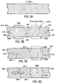
Figure 1 illustrates a buildup layer and a metallic core layer assembly. -
Figure 2A shows a buildup layer. -
Figure 2B shows an imprinted buildup layer. -
Figure 2C shows an imprinted buildup layer filled with conductive material. -
Figure 3A shows a metallic core layer. -
Figure 3B illustrates an AlOx/Al core layer with photo resist mask applied thereto in a first pattern. -
Figure 3C illustrates an AlOx/Al core layer with photo resist mask applied thereto in a second pattern. -
Figure 3D an AlOx/Al core layer after planarization. -
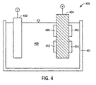
Figure 4 illustrates an anodizing process. - In the following detailed description, numerous specific details are set forth. However, it is understood that embodiments of the invention may be practiced without these specific details. In other instances, well-known circuits, structures, and techniques have not been shown in detail in order not to obscure the understanding of this description. The following detailed description is, therefore, not to be taken in a limiting sense, and the scope of the invention is defined only by the appended claims.
- A metallic core layer fabricated by anodization or similar process is laminated to an imprinted-buildup layer to create a multilayer integrated circuit package. Using imprinting and selective anodic oxidation processes eliminates a number of process steps for creating conductive traces of various depth and vias in the buildup layer and creating plated through holes in the core layer. Following the methods described herein, the vias and any number of different depth/size circuit traces are made in one or both sides of the buildup layer simultaneously. The separate step of filling the vias with metal is eliminated. Distinct conductive regions and nonconductive regions are created in a metallic core layer by selective anodic oxidation. The combination of conductive and non-conductive regions form circuit traces on one or both sides of the metallic core layer. Additional metallic core layers or additional buildup layers can be added to the multilayer integrated circuit package to create additional circuit layers as required by a given integrated circuit package design.
- Each buildup layer and each metallic layer, can on each of their respective sides, support a layer of circuit traces and either passive or active devices, attached thereto. Thus, resistors or capacitors can be attached or incorporated into a surface of either the metallic layer or the buildup layer. In various embodiments, these active or passive devices will either be mounted to the outer surface(s) of the integrated circuit package or be contained within layers of the integrated circuit package. In the following description, Aluminum (Al) will be used for the metallic layer. Non-conductive regions formed therein will be an oxide thereof, Aluminum Oxide (AlOx).
- In one embodiment,
Figure 1 illustrates a cross sectional view of a buildup layer and a metalliccore layer assembly 100. The view presented inFigure 1 is a segment of the assembly. With reference toFigure 1 , acore layer 104 contains a non-conductive or dielectric region made of Aluminum Oxide (AlOx) 104a and a conductive region made of Aluminum (Al) 104b. Adjacent to thecore layer 104 is abuildup layer 102. Thebuildup layer 102 contains adielectric region 102a and aconductive region 102b. In one embodiment, thedielectric region 102a can be made from a Liquid Crystal Polymer (LCP), such as R/max™ from Rogers Corp. Disposed between the AlOxregion 104a of thecore layer 104 and thedielectric region 102a is anadhesive layer 106.Adhesive layer 106 provides bonding between the AlOxregion 104a and thedielectric region 102a of thebuildup layer 102. In one embodiment, theadhesive layer 106 is made from a low melting point Liquid Crystal Polymer (LCPLM). An appropriate LCPLM material will depend on the material selected for the LCP, which is used for thedielectric region 102a. Some examples of other materials that can be suitable for use as thedielectric region 102a are epoxy, polyethelene and other thermoset and thermoplastic polymers. - In one embodiment, epoxy can be used as the material for the
buildup layer 102. In this embodiment, theadhesive layer 106 can be made from the same epoxy as was used for thebuildup layer 102, except that theadhesive layer 106 would not be fully cured at the time thecore layer 104 was laminated to builduplayer 102, such thatadhesive layer 106 still flowed when heated during lamination. - Disposed between the
Al region 104b andconductive region 102b is ametallic contact 108. Themetallic contact 108 provides electrical continuity betweensurface 110 andsurface 112. TheAl region 104b can function as a plated through hole or via within thecore layer 104. TheAl region 104b in combination with themetallic contact 108 and theconductive region 102b provide the equivalent of a via through the entire thickness of theassembly 100. - The
metallic contact 108 can be a layer of solder paste applied to theAl region 104b via a screen printing process as is well known in the art. Commercially available solder paste can be used formetallic contact 108. A tin/silver alloy consisting of 3.5% silver is suitable as well as other solder paste that melts below the melting point of thebuildup layer 102. In another embodiment of the invention, the metallic contact can be made with a solder ball placed under compression and/or partially or fully melted by the lamination of thecore layer 104 and thebuildup layer 102. In yet another embodiment of the invention, themetallic contact 108 can be made using a pre-stressed metallic contact that exerts contact pressure on the opposing faces once placed under lamination pressure conditions. Although the metallic contacts were described with respect to various embodiments of the invention, an embodiment of the invention can be made that includes several different techniques for making the metallic contact and/or theadhesive layer 106 withinassembly 100. Thus, the described embodiments of the invention may be combined as needed to achieve the desired results and are not mutually exclusive of one another. - The
assembly 100 can be made in a variety of ways. In one embodiment of the invention, the adhesive 106 can be applied to one surface ofcore layer 104. The adhesive 106 is then removed from the surface of theAl region 104b by laser oblation. Alternatively, the adhesive may be removed from the surface of theAl region 104b by using photolithography plus a chemical etch. Following this alternative approach, a layer of photo resist is applied to the surface of the adhesive layer except for that region of the adhesive in contact with theAl region 104b which is intended for removal. The chemical etch would then remove the adhesive layer in contact withAl region 104b. Solder paste can be applied to the surface of the Al region where the adhesive 106 was just removed. In one embodiment, the solder paste can be screen printed to the surface of the Al. Alternatively, another mechanism can be used for themetallic contact 108, such as a pre-stressed metallic contact described below, in place of the solder paste. - The
core layer 104 is aligned with thebuildup layer 102 so that the circuit features contained within each layer, 102 and 104, will mate in the intended way according to the circuit design for each layer. As mentioned above thecore layer 104 is laminated to thebuildup layer 102. The lamination may be performed under a very broad range of conditions. The exact lamination conditions will depend on the particular materials such as LCP, LCPLM adhesive, solder, and/or other metallic contact means employed within theassembly 100. Typical lamination conditions for an LCP/copper buildup layer 102 and the AlOx/Al core layer 104 are 500 degrees Fahrenheit at a pressure of 200 pounds per square inch for 30 minutes. In this example, R/max™ can be used for the LCP. During lamination, the application of heat and pressure causes the solder paste to melt adhering theAl region 104b to theconductive region 102b. Similarly, theadhesive layer 106 causes theAlOx region 104a to be bonded to thedielectric region 102a. In an alternative embodiment, when one of the alternative forms of making themetallic contact 108 is employed, the pressure applied during lamination will deform the pre-stressed metallic contact and/or the solder ball. The bond achieved between the core layer and the buildup layer under lamination pressure conditions provides pressure between theAl region 104b andconductive region 102b, thereby ensuring that the required metallic contact is achieved. - The layers and regions previously described contain a third dimension providing extent into the plane of
Figure 1 . According to various embodiments of the invention, the layers and regions previously described may vary from the lengths shown inFigure 1 . No limitation on the invention is implied by the view presented inFigure 1 . Thus, theAl region 104b can have a round cross section or any shape necessitated by the given design. Aconductive region 102c can be in contact with theconductive region 102b and can be one continuous piece of conductive material such as copper. In alternative embodiments, conductive polymer, solder, and other conductors can be used in place of copper. Theconductive region 102c can be part of a circuit existing in a first layer of circuitry within theassembly 100 and the conductive path between 112 and 110 provides electrical continuity with other planes of circuitry existing at different depths within theassembly 100. Theassembly 100 is capable of containing two planes of circuitry per buildup layer or AlOx core layer, however to preserve clarity in the illustration only a minimum number of conductive circuit traces 102c, 102b, and 104b have been included in the view presented byFigure 1 . In general, as discussed previously, a layer of circuit traces and devices can be formed into each side of either thebuildup layer 102 or thecore layer 104. - A process for creating the imprinted buildup layer, such as the one shown in
Figure 1 at 102 is illustrated inFigures 2A, 2B, and 2C . With respect toFigure 2A , the process starts with a layer ofbuildup material 202 as shown inFigure 2A . The layer ofbuildup material 202 can be LCP as was previously discussed in conjunction withFigure 1 , or another material such as epoxy. The material properties required for the buildup material are the ability to tolerate and maintain a permanent state of plastic deformation and to have the electrical property of a dielectric. - A pattern is imprinted into the surface of
buildup material 202 with the use ofupper imprinting tool 210a andlower imprinting tool 210b as seen withinFigure 2B . Theupper imprinting tool 210a is moved in the direction indicated byarrow 212a. Thelower imprinting tool 210b is moved in the direction indicated byarrow 212b. Pressing the imprinting tools intobuildup material 202 results in the formation of a void 214 and avoid 216. The series of voids that are made during the embossing operation results in one or more circuit lines being molded into the buildup material 202 (Figure 2B ). These voids become circuit lines once the voids are filled with conductive material such as copper and the surface is planarized, as described below. The through holes that result from the embossing operation and a subsequent surface cleaning step result in the formation of vias once the through holes are filed with conductive material such as copper. - Typical nominal dimensions of a
width 222 of the void 216 are 5 microns with a depth of 5 to 10 microns (Figure 2B and Figure 2C ). The typical thickness of thebuildup layer 202 is 15-20 microns. Variations from these dimensions are contemplated within the scope of the present invention. The present invention is not limited by the dimensions imprinted into thebuildup material 202. - The
imprinting tools buildup material 202 it is necessary for the imprinting tool to sustain the forces of imprinting within acceptable limits of wear. Thus, the imprinting tool must necessarily be made from a material that is harder than the material used for the buildup layer. Acceptable limits of wear will be determined by a given application. The present invention is not limited by the material chosen for theimprinting tools buildup material 202 with the use of the single imprinting tool and the planar surface. - After the imprinting process, the surfaces of the
buildup material 202 must be cleaned (Figure 2B ). In one embodiment, the surfaces are cleaned and roughened with a plasma process. Submicron layers of surface material are removed with the plasma cleaning process. During the imprinting process, certain imprinted features, like the through hole for the via, will result in thin slices and/or pieces of material being left in the void, blocking or partially blocking the void 214 which must be removed during the etching process. Following the cleaning process a seed layer of metal is applied via sputtering or by immersing the polymer in a liquid catalyst. During the sputtering process chrome-copper can be used as the sputtered metal. - In an alternative embodiment, the surfaces can be cleaned and roughened with a chemical etch using a wet etch of sodium permanganate or potassium permanganate. During immersion in the liquid catalyst the emulsion of palladium chloride is absorbed to the surface leaving a very thin layer of palladium over the surface of the
buildup layer 202. - The next process is an electroplating process, where a conductive material such as copper is deposited into all of the
voids buildup material 202 resulting inconductive material 218 filling thevoids Figure 2C . Following the electroplating process, the surface of 202 is planarized resulting in the layer shown inFigure 2C . The layer shown inFigure 2C can be planarized using the techniques that are well known in the art. Planarization of the buildup layer (Figure 2C ) can be achieved by precision grinding the surface using an abrasive brush, an abrasive impregnated compressed organic fiber, sandpaper or an equivalent as is known in the art. Planarization removes the deposited conductive material from the outer surfaces ofbuildup material 202 and leaves theconductive material 218 within the confines of thevoids 214 and 216 (Figure 2C ). The present invention is not limited by the materials or processes chosen for cleaning, roughening, and/or metalizing the buildup layers. - Electrochemical anodic oxidation (anodization) is used to convert Al into AlOx. In one embodiment of the invention,
Figures 3A, 3B, 3C, and 3D illustrate the process of forming a metallic core layer from a layer of Al by partially anodizing the Al layer. Exposing the Al layer to an anodizing process converts Al into AlOx, a dielectric. The distribution of AlOx and Al within the layer is displayed at four instances in time, using the cross sectional views shown inFigures 3A, 3B, 3C, and 3D . The process begins with a conductive layer, in this example a layer ofAl 302a as shown at time T1 (Figure 3A ). Photo resist 304a, 304b, 306a, and 306b are applied to theAl 302a layer to prevent anodizing from occurring beneath the areas of photo resist. The anodizing process continues untilphase fronts 310 have been formed (Figure 3B ). Distinct regions ofAlOx 308 andAl 302b are now created within the layer shown inFigure 3B . -
Figure 4 displays an arrangement in which electrochemical anodic oxidation can be performed. With respect toFigure 4 ,tank 401 contains asolution 406 of weak organic acid or inorganic acid, e.g., boric acid, formic acid, citric acid, etc., or a combination thereof. Acathode 402 and themetallic layer 404 are shown immersed in thesolution 406. Themetallic layer 404 functions as an anode. The combination of thecathode 402, theanode 404, thesolution 406, and an appropriate source of current (not shown) constitutes a galvanic cell. Current is supplied to the system by placing thecathode 402 and theanode 404 at different electrical potentials. During anodizing, selective oxidation of the surface of theanode 404 occurs such that conversion of the conductive regions into non-conductive regions occurs. Exposed regions of the surface of 404, not covered by maskingregions Figures 3A, 3B, 3C, and 3D , aluminum was the material used to make the conductive region and the aluminum is converted into nonconductive AlOx during anodization. If a different metallic material was used to make the conductive region in the anode, then the converted nonconductive regions will be the respective oxide of the metallic material. - In various embodiments of the invention, process parameters can be adjusted to achieve the desired sequence of conductive and non-conductive regions within the core layer. Two types of non-conductive regions can be formed within the aluminum; a porous and a non-porous region. The porous layer provides the required non-conductive property of the dielectric. The dense region acts as a barrier, protecting conductive regions from the oxidation process currently taking place within an adjacent upper layer. It should be noted that porous or dense regions can be created within each core layer and may exist either singly or in combination with each other in a given core layer. Described below are several non-limiting examples that can be used for the anodizing process to create both porous and non-porous layers.
- In the embodiment of the invention described in the following paragraphs the metallic component of the
anode 404 is selected to be aluminum. It should be noted that the anode could have been made out of another conductive material other than aluminum, in that case the converted nonconductive regions will be the respective oxide of the metallic material chosen for the anode. - A multi-component electrolyte solution is prepared having oxalic acid with a concentration of 70 grams/liter, citric acid having a concentration of 40 g/liter, and boric acid having a concentration of 16g/liter. The previously listed acids are mixed in a 1:1:1 proportion and achieve an electrolytic solution having a pH of 1.5. In a first step, anodizing proceeds with a voltage gradient of 1-2 volts/sec from 0 volts up to approximately 40 volts for 40 seconds. In a second step, another set of process parameters keeps the voltage relatively constant at approximately 40 volts for approximately 10-30 minutes until a current density is established in the range of 1-2 ampers/dm2. Anodic oxidation effected according to this process will result in the formation of AlOx to a depth of approximately 2-3 micron. In the alternative, current density can be monitored to determine the depth of anodizing achieved. For example anodic oxidation can be terminated when the current density falls below 8-9 milliamper/dm2. In practice, AlOx regions with thicknesses of up to 20 microns can be obtained provided the thickness of the original unoxidized aluminum layer is sufficiently thick. It is possible to oxidize the entire thickness of the aluminum layer if the anodizing process is allowed to proceed until the current density measures approximately zero.
- A dense region can be used as a barrier to prevent a subsequent anodizing process from changing the character of material situated below or under the barrier. The following non-limiting example of the use of a barrier is provided herein to illustrate one embodiment of using the invention to create a dense region. The process contains the following two steps. First the voltage is increased in a stepwise fashion by increasing the gradient from 1-2 volts from 0 volts up to 300 volts for approximately 5 minutes. Secondly, oxidation proceeds at constant voltage 150-300 volts for approximately 20 minutes until the current density increases from approximately 4 microamperes/dm2 up to 0.05-0.07 ampere/dm2. This current density is associated with the formation of the dense region which has a thickness of 0.02-0.07 microns.
- In one or more embodiments of the invention, photo resist can be used to create internal regions of Al that are disconnected from the surfaces of the layer. To create such a feature, the process will proceed with the removal of photo resist 306a, 306b, 304a, and 304b (
Figure 3B ). Photo resistmask Figure 3C . Anodizing begins again and continues to convert Al to AlOx.Phase fronts 310, inFigure 3B , change intophase fronts Figure 3C , thereby creating anAl region 302c which is not in contact with either ofsurfaces 318 or 320 (Figure 3D ). -
Al region 302d extends across the entire width of the layer and was created by keeping photo resist in the locations indicated by 304a and 304b while the anodizing process was in progress. Various embodiments of the invention are possible by combining the previously described steps of applying and removing photo resist and stripping and restarting the anodizing process in order to create various distributions of AlOx and Al. In the previous discussion, directed to forming theAl region 302c, an alternative series of processes could have achieved the same final result. For example, photo resist 306a and 306b could have been absent during the first anodizing process and present during the second anodizing process. The same result is achieved, e.g., a region of Al disconnected fromsurfaces - Following the anodizing process, the layers of photo resist are removed using conventional chemical processing as is known in the art and the
surfaces plane 318 and/or 320. During lamination, the bump provided by the Al region will compress and make contact with the adjacent conductive region of the buildup layer. This is one example of the pre-stressed metallic contact mentioned in an earlier section. - In various embodiments of the invention, a plurality of regions in both the
core layer 104 and thebuildup layer 102, such as but not limited to those indicated byconductive region 102c anddielectric region 102a (Figure 1 ), will be used to make an integrated circuit package that will be used to connect together one or more integrated circuits and or passive or active circuit elements. Integrated circuit packages made according to the teachings of the invention can be used wherever integrated circuits are presently used, eg., in camcorders, cellular telephones, personal data assistants, laptop computers, desktop computers, desk side computers, servers, etc. - While the invention has been described in terms of several embodiments, those of ordinary skill in the art will recognize that the invention is not limited to the embodiments described, but can be practiced with modification and alteration within the scope of the appended claims. The description is thus to be regarded as illustrative instead of limiting.
Claims (29)
- A method comprising:applying adhesive material (106) to a metallic core layer (104);removing adhesive material from a conductive region (104b) of the metallic core layer;providing a metallic contact (108) over the conductive region (104b) of the metallic core layer; andlaminating the metallic core layer (104) to a buildup layer (102), the buildup layer having a dielectric region (102a) and a conductive region (102b), wherein a nonconductive region (104a) of the metallic core layer (104) is bonded to the dielectric region (102a) of the buildup layer (102) and the conductive region (104b) of the metallic core layer is bonded to the conductive region (102b) of the buildup layer (102).
- The method of claim 1, wherein an integrated circuit package is formed having four or more circuit layers.
- The method of claim 1, wherein solder paste is used to make the metallic contact.
- The method of claim 3, wherein the solder paste is screen-printed.
- The method of claim 1, wherein a solder ball is used to make the metallic contact.
- The method of claim 1, wherein a pre-stressed metallic contact is used to make the metallic contact.
- The method of claim 1, wherein a liquid crystal polymer layer (LCP) is used for the adhesive material.
- The method of claim 1, wherein the laminating is performed at 260 degrees Celsius (500 degrees Fahrenheit), 1,37895 MPa (200 pounds per square inch) for 30 minutes.
- The method of claim 1, wherein the dielectric region of the buildup layer is a liquid crystal polymer.
- The method of claim 1, wherein the conductive region of the buildup layer is copper.
- The method of claim 1, wherein the conductive region of the metallic core layer is aluminum, Al.
- The method of claim 1, wherein the non-conductive region of the metallic core layer is Aluminum oxide, AlOx.
- A method comprising:applying adhesive material (106) to a metallic core layer (104), wherein the adhesive material is applied to a surface of a nonconductive region (104a) of the metallic core layer (104);providing a metallic contact (108) over a surface of a conductive region (104b) of the metallic core layer; andlaminating the metallic core layer (104) to a buildup layer (102), the buildup layer having a dielectric region (102a) and a conductive region (102b), wherein the surface of the nonconductive region (104a) of the metallic core layer (104) is bonded to a surface of the dielectric region (102a) of the buildup layer (102) and the surface of the conductive region (104b) of the metallic core layer is bonded to a surface of the conductive region (102b) of the buildup layer (102).
- The method of claim 13, further comprising removing the adhesive material from the surface of the conductive region of the metallic core layer with laser ablation.
- The method of claim 13, further comprising removing the adhesive material from the surface of the conductive region of the metallic core layer with a lithium chemical etch.
- The method of claim 13, wherein the conductive region of the metallic core layer is aluminum, Al.
- The method of claim 13, wherein the non-conductive region of the metallic core layer is Aluminum oxide, AlOx.
- An apparatus comprising:a core layer (104) having a non-conductive region (104a) and a conductive region (104b), wherein the non-conductive region (104a) was formed by anodizing;a buildup layer (102) being a dielectric region (102a) and a conductive region (102b), wherein the buildup layer was formed by imprinting and metallizing the dielectric region (102a),an adhesive layer (106), wherein the adhesive layer is used to adhere the non-conductive region of the core layer (104) to the dielectric region of the buildup layer (102); anda metallic contact (108), wherein the metallic contact provides electric continuity between the conductive region (104b) of the core layer and the conductive region (102b) of the buildup layer (102).
- The apparatus of claim 18, wherein an integrated circuit package is formed having four circuit layers.
- The apparatus of claim 18, wherein solder paste is used to make the metallic contact.
- The apparatus of claim 20, wherein the solder paste is screen-printed.
- The apparatus of claim 18, wherein a solder ball is used to make the metallic contact.
- The apparatus of claim 18, wherein a pre-stressed metallic contact is used to make the metallic contact.
- The apparatus of claim 18, wherein a liquid crystal polymer layer (LCP) is used for the adhesive material.
- The apparatus of claim 18, wherein the dielectric region of the core layer is a liquid crystal polymer.
- The apparatus of claim 18, wherein the metallic region of the core layer is copper.
- The apparatus of claim 18, wherein the conductive region of the core layer is aluminum, Al.
- The apparatus of claim 18, wherein the non-conductive region of the core layer is Aluminum oxide, AlOx.
- The apparatus of claim 18, further comprising:memory;a system bus coupled with the memory; andan integrated circuit imbedded in the apparatus, wherein the apparatus processes data.
Applications Claiming Priority (3)
| Application Number | Priority Date | Filing Date | Title |
|---|---|---|---|
| US109792 | 2002-03-29 | ||
| US10/109,792 US6899815B2 (en) | 2002-03-29 | 2002-03-29 | Multi-layer integrated circuit package |
| PCT/US2003/008835 WO2003086038A1 (en) | 2002-03-29 | 2003-03-21 | Multi-layer integrated circuit package |
Publications (2)
| Publication Number | Publication Date |
|---|---|
| EP1491078A1 EP1491078A1 (en) | 2004-12-29 |
| EP1491078B1 true EP1491078B1 (en) | 2010-06-23 |
Family
ID=28453172
Family Applications (1)
| Application Number | Title | Priority Date | Filing Date |
|---|---|---|---|
| EP03746044A Expired - Lifetime EP1491078B1 (en) | 2002-03-29 | 2003-03-21 | Multi-layer integrated circuit package |
Country Status (8)
| Country | Link |
|---|---|
| US (2) | US6899815B2 (en) |
| EP (1) | EP1491078B1 (en) |
| CN (1) | CN100441074C (en) |
| AT (1) | ATE472242T1 (en) |
| AU (1) | AU2003225932A1 (en) |
| DE (1) | DE60333084D1 (en) |
| MY (1) | MY132766A (en) |
| WO (1) | WO2003086038A1 (en) |
Families Citing this family (11)
| Publication number | Priority date | Publication date | Assignee | Title |
|---|---|---|---|---|
| US7368045B2 (en) * | 2005-01-27 | 2008-05-06 | International Business Machines Corporation | Gate stack engineering by electrochemical processing utilizing through-gate-dielectric current flow |
| JP5072283B2 (en) * | 2006-07-31 | 2012-11-14 | 三洋電機株式会社 | Circuit board |
| KR100815361B1 (en) | 2007-01-31 | 2008-03-19 | 삼성전기주식회사 | Process for manufacturing printed circuit board |
| JP2009200338A (en) * | 2008-02-22 | 2009-09-03 | Renesas Technology Corp | Method for manufacturing semiconductor device |
| JP2011014612A (en) * | 2009-06-30 | 2011-01-20 | Ibiden Co Ltd | Wiring board and method for manufacturing wiring board |
| US8304863B2 (en) | 2010-02-09 | 2012-11-06 | International Business Machines Corporation | Electromigration immune through-substrate vias |
| US8867219B2 (en) * | 2011-01-14 | 2014-10-21 | Harris Corporation | Method of transferring and electrically joining a high density multilevel thin film to a circuitized and flexible organic substrate and associated devices |
| KR102103375B1 (en) | 2013-06-18 | 2020-04-22 | 삼성전자주식회사 | A semiconductor package |
| DE102014220650A1 (en) * | 2014-10-13 | 2016-04-14 | Heraeus Deutschland GmbH & Co. KG | Optimized trace design of metallic materials on ceramic substances |
| US9865527B1 (en) * | 2016-12-22 | 2018-01-09 | Texas Instruments Incorporated | Packaged semiconductor device having nanoparticle adhesion layer patterned into zones of electrical conductance and insulation |
| US9941194B1 (en) | 2017-02-21 | 2018-04-10 | Texas Instruments Incorporated | Packaged semiconductor device having patterned conductance dual-material nanoparticle adhesion layer |
Family Cites Families (12)
| Publication number | Priority date | Publication date | Assignee | Title |
|---|---|---|---|---|
| US4146440A (en) * | 1978-04-03 | 1979-03-27 | Burroughs Corporation | Method for forming an aluminum interconnect structure on an integrated circuit chip |
| US5917157A (en) * | 1994-12-12 | 1999-06-29 | Remsburg; Ralph | Multilayer wiring board laminate with enhanced thermal dissipation to dielectric substrate laminate |
| US6395582B1 (en) * | 1997-07-14 | 2002-05-28 | Signetics | Methods for forming ground vias in semiconductor packages |
| US6159586A (en) * | 1997-09-25 | 2000-12-12 | Nitto Denko Corporation | Multilayer wiring substrate and method for producing the same |
| US6326555B1 (en) * | 1999-02-26 | 2001-12-04 | Fujitsu Limited | Method and structure of z-connected laminated substrate for high density electronic packaging |
| US6204089B1 (en) * | 1999-05-14 | 2001-03-20 | Industrial Technology Research Institute | Method for forming flip chip package utilizing cone shaped bumps |
| JP3514669B2 (en) | 1999-06-30 | 2004-03-31 | 三菱樹脂株式会社 | Metal-based printed wiring board, metal-based multilayer printed wiring board, and method of manufacturing the same |
| JP4201436B2 (en) | 1999-07-14 | 2008-12-24 | 日東電工株式会社 | Manufacturing method of multilayer wiring board |
| US6525921B1 (en) * | 1999-11-12 | 2003-02-25 | Matsushita Electric Industrial Co., Ltd | Capacitor-mounted metal foil and a method for producing the same, and a circuit board and a method for producing the same |
| TWI226814B (en) * | 1999-12-16 | 2005-01-11 | Matsushita Electric Ind Co Ltd | A removable film, a substrate with film, a process for forming the removable film and a process for the manufacturing of the circuit board |
| JP2001320171A (en) * | 2000-05-08 | 2001-11-16 | Shinko Electric Ind Co Ltd | Multilayer wiring board and semiconductor device |
| US6585903B1 (en) * | 2000-09-06 | 2003-07-01 | Visteon Global Tech. Inc. | Electrical circuit board and a method for making the same |
-
2002
- 2002-03-29 US US10/109,792 patent/US6899815B2/en not_active Expired - Fee Related
-
2003
- 2003-03-21 AU AU2003225932A patent/AU2003225932A1/en not_active Abandoned
- 2003-03-21 WO PCT/US2003/008835 patent/WO2003086038A1/en not_active Application Discontinuation
- 2003-03-21 AT AT03746044T patent/ATE472242T1/en not_active IP Right Cessation
- 2003-03-21 CN CNB03811318XA patent/CN100441074C/en not_active Expired - Fee Related
- 2003-03-21 DE DE60333084T patent/DE60333084D1/de not_active Expired - Lifetime
- 2003-03-21 EP EP03746044A patent/EP1491078B1/en not_active Expired - Lifetime
- 2003-03-27 MY MYPI20031130A patent/MY132766A/en unknown
-
2004
- 2004-08-11 US US10/915,803 patent/US7245001B2/en not_active Expired - Fee Related
Also Published As
| Publication number | Publication date |
|---|---|
| DE60333084D1 (en) | 2010-08-05 |
| WO2003086038A1 (en) | 2003-10-16 |
| US6899815B2 (en) | 2005-05-31 |
| US20030184987A1 (en) | 2003-10-02 |
| CN1653874A (en) | 2005-08-10 |
| US20050009353A1 (en) | 2005-01-13 |
| MY132766A (en) | 2007-10-31 |
| AU2003225932A1 (en) | 2003-10-20 |
| ATE472242T1 (en) | 2010-07-15 |
| EP1491078A1 (en) | 2004-12-29 |
| CN100441074C (en) | 2008-12-03 |
| US7245001B2 (en) | 2007-07-17 |
Similar Documents
| Publication | Publication Date | Title |
|---|---|---|
| KR100203540B1 (en) | Circuit devices and fabrication method of the same | |
| US5440805A (en) | Method of manufacturing a multilayer circuit | |
| US8222539B2 (en) | Wiring board and method for manufacturing the same | |
| KR100427794B1 (en) | Method of manufacturing multilayer wiring board | |
| TW200524502A (en) | Method of providing printed circuit board with conductive holes and board resulting therefrom | |
| EP1491078B1 (en) | Multi-layer integrated circuit package | |
| US20080264677A1 (en) | Circuit board structure having embedded capacitor and fabrication method thereof | |
| KR100690480B1 (en) | Connection Substrate, Multilayer Wiring Board Using the Connection Substrate, Substrate for Semiconductor Package, Semiconductor Package, and Methods for Manufacturing Them | |
| KR100857165B1 (en) | Method for manufacturing circuit board | |
| JP4449975B2 (en) | Connection board, multilayer wiring board using the connection board, and methods of manufacturing the same | |
| JP4060629B2 (en) | Method for forming plated through hole and method for manufacturing multilayer wiring board | |
| US7278205B2 (en) | Multilayer printed wiring board and production method therefor | |
| CN100521878C (en) | Method for producing multilayer printed wiring board | |
| JP2005268378A (en) | Method of manufacturing substrate with incorporated components | |
| CN101641461B (en) | Multilayer printed wiring boards with copper filled through-holes | |
| JP3862454B2 (en) | Metal-based multilayer circuit board | |
| JP2003298212A (en) | Printed wiring board and manufacturing method thereof | |
| CN117241466B (en) | Liquid cooling circuit board with embedded device and preparation method thereof | |
| KR100448685B1 (en) | method for manufacturing build-up multi-layer printed circuit board | |
| KR100827310B1 (en) | Printed Circuit Board and the method of manufacturing thereof | |
| JP2003318534A (en) | Interlayer connecting structure and its forming method | |
| JP2023013121A (en) | Wiring board and manufacturing method of wiring board | |
| JP2004207266A (en) | Method for manufacturing connection substrate and multilayer wiring board | |
| JP2005150447A (en) | Wiring board and its manufacturing method | |
| CN116390350A (en) | Preparation method of POFV pore structure |
Legal Events
| Date | Code | Title | Description |
|---|---|---|---|
| PUAI | Public reference made under article 153(3) epc to a published international application that has entered the european phase |
Free format text: ORIGINAL CODE: 0009012 |
|
| 17P | Request for examination filed |
Effective date: 20040930 |
|
| AK | Designated contracting states |
Kind code of ref document: A1 Designated state(s): AT BE BG CH CY CZ DE DK EE ES FI FR GB GR HU IE IT LI LU MC NL PT RO SE SI SK TR |
|
| AX | Request for extension of the european patent |
Extension state: AL LT LV MK |
|
| RIN1 | Information on inventor provided before grant (corrected) |
Inventor name: WALK, MICHAEL Inventor name: COOMER, BOYD |
|
| GRAP | Despatch of communication of intention to grant a patent |
Free format text: ORIGINAL CODE: EPIDOSNIGR1 |
|
| GRAS | Grant fee paid |
Free format text: ORIGINAL CODE: EPIDOSNIGR3 |
|
| GRAA | (expected) grant |
Free format text: ORIGINAL CODE: 0009210 |
|
| AK | Designated contracting states |
Kind code of ref document: B1 Designated state(s): AT BE BG CH CY CZ DE DK EE ES FI FR GB GR HU IE IT LI LU MC NL PT RO SE SI SK TR |
|
| REG | Reference to a national code |
Ref country code: CH Ref legal event code: EP |
|
| REG | Reference to a national code |
Ref country code: IE Ref legal event code: FG4D |
|
| REF | Corresponds to: |
Ref document number: 60333084 Country of ref document: DE Date of ref document: 20100805 Kind code of ref document: P |
|
| REG | Reference to a national code |
Ref country code: NL Ref legal event code: VDEP Effective date: 20100623 |
|
| PG25 | Lapsed in a contracting state [announced via postgrant information from national office to epo] |
Ref country code: SE Free format text: LAPSE BECAUSE OF FAILURE TO SUBMIT A TRANSLATION OF THE DESCRIPTION OR TO PAY THE FEE WITHIN THE PRESCRIBED TIME-LIMIT Effective date: 20100623 |
|
| PG25 | Lapsed in a contracting state [announced via postgrant information from national office to epo] |
Ref country code: SI Free format text: LAPSE BECAUSE OF FAILURE TO SUBMIT A TRANSLATION OF THE DESCRIPTION OR TO PAY THE FEE WITHIN THE PRESCRIBED TIME-LIMIT Effective date: 20100623 Ref country code: AT Free format text: LAPSE BECAUSE OF FAILURE TO SUBMIT A TRANSLATION OF THE DESCRIPTION OR TO PAY THE FEE WITHIN THE PRESCRIBED TIME-LIMIT Effective date: 20100623 Ref country code: FI Free format text: LAPSE BECAUSE OF FAILURE TO SUBMIT A TRANSLATION OF THE DESCRIPTION OR TO PAY THE FEE WITHIN THE PRESCRIBED TIME-LIMIT Effective date: 20100623 |
|
| PG25 | Lapsed in a contracting state [announced via postgrant information from national office to epo] |
Ref country code: GR Free format text: LAPSE BECAUSE OF FAILURE TO SUBMIT A TRANSLATION OF THE DESCRIPTION OR TO PAY THE FEE WITHIN THE PRESCRIBED TIME-LIMIT Effective date: 20100924 |
|
| PG25 | Lapsed in a contracting state [announced via postgrant information from national office to epo] |
Ref country code: EE Free format text: LAPSE BECAUSE OF FAILURE TO SUBMIT A TRANSLATION OF THE DESCRIPTION OR TO PAY THE FEE WITHIN THE PRESCRIBED TIME-LIMIT Effective date: 20100623 Ref country code: NL Free format text: LAPSE BECAUSE OF FAILURE TO SUBMIT A TRANSLATION OF THE DESCRIPTION OR TO PAY THE FEE WITHIN THE PRESCRIBED TIME-LIMIT Effective date: 20100623 |
|
| PG25 | Lapsed in a contracting state [announced via postgrant information from national office to epo] |
Ref country code: CY Free format text: LAPSE BECAUSE OF FAILURE TO SUBMIT A TRANSLATION OF THE DESCRIPTION OR TO PAY THE FEE WITHIN THE PRESCRIBED TIME-LIMIT Effective date: 20100623 Ref country code: BE Free format text: LAPSE BECAUSE OF FAILURE TO SUBMIT A TRANSLATION OF THE DESCRIPTION OR TO PAY THE FEE WITHIN THE PRESCRIBED TIME-LIMIT Effective date: 20100623 Ref country code: RO Free format text: LAPSE BECAUSE OF FAILURE TO SUBMIT A TRANSLATION OF THE DESCRIPTION OR TO PAY THE FEE WITHIN THE PRESCRIBED TIME-LIMIT Effective date: 20100623 Ref country code: SK Free format text: LAPSE BECAUSE OF FAILURE TO SUBMIT A TRANSLATION OF THE DESCRIPTION OR TO PAY THE FEE WITHIN THE PRESCRIBED TIME-LIMIT Effective date: 20100623 Ref country code: PT Free format text: LAPSE BECAUSE OF FAILURE TO SUBMIT A TRANSLATION OF THE DESCRIPTION OR TO PAY THE FEE WITHIN THE PRESCRIBED TIME-LIMIT Effective date: 20101025 Ref country code: CZ Free format text: LAPSE BECAUSE OF FAILURE TO SUBMIT A TRANSLATION OF THE DESCRIPTION OR TO PAY THE FEE WITHIN THE PRESCRIBED TIME-LIMIT Effective date: 20100623 |
|
| PG25 | Lapsed in a contracting state [announced via postgrant information from national office to epo] |
Ref country code: IT Free format text: LAPSE BECAUSE OF FAILURE TO SUBMIT A TRANSLATION OF THE DESCRIPTION OR TO PAY THE FEE WITHIN THE PRESCRIBED TIME-LIMIT Effective date: 20100623 |
|
| PG25 | Lapsed in a contracting state [announced via postgrant information from national office to epo] |
Ref country code: DK Free format text: LAPSE BECAUSE OF FAILURE TO SUBMIT A TRANSLATION OF THE DESCRIPTION OR TO PAY THE FEE WITHIN THE PRESCRIBED TIME-LIMIT Effective date: 20100623 |
|
| PLBE | No opposition filed within time limit |
Free format text: ORIGINAL CODE: 0009261 |
|
| STAA | Information on the status of an ep patent application or granted ep patent |
Free format text: STATUS: NO OPPOSITION FILED WITHIN TIME LIMIT |
|
| 26N | No opposition filed |
Effective date: 20110324 |
|
| REG | Reference to a national code |
Ref country code: DE Ref legal event code: R097 Ref document number: 60333084 Country of ref document: DE Effective date: 20110323 |
|
| PG25 | Lapsed in a contracting state [announced via postgrant information from national office to epo] |
Ref country code: MC Free format text: LAPSE BECAUSE OF NON-PAYMENT OF DUE FEES Effective date: 20110331 |
|
| REG | Reference to a national code |
Ref country code: CH Ref legal event code: PL |
|
| REG | Reference to a national code |
Ref country code: FR Ref legal event code: ST Effective date: 20111130 |
|
| REG | Reference to a national code |
Ref country code: IE Ref legal event code: MM4A |
|
| PG25 | Lapsed in a contracting state [announced via postgrant information from national office to epo] |
Ref country code: CH Free format text: LAPSE BECAUSE OF NON-PAYMENT OF DUE FEES Effective date: 20110331 Ref country code: FR Free format text: LAPSE BECAUSE OF NON-PAYMENT OF DUE FEES Effective date: 20110331 Ref country code: LI Free format text: LAPSE BECAUSE OF NON-PAYMENT OF DUE FEES Effective date: 20110331 Ref country code: IE Free format text: LAPSE BECAUSE OF NON-PAYMENT OF DUE FEES Effective date: 20110321 |
|
| PG25 | Lapsed in a contracting state [announced via postgrant information from national office to epo] |
Ref country code: LU Free format text: LAPSE BECAUSE OF NON-PAYMENT OF DUE FEES Effective date: 20110321 |
|
| PG25 | Lapsed in a contracting state [announced via postgrant information from national office to epo] |
Ref country code: BG Free format text: LAPSE BECAUSE OF FAILURE TO SUBMIT A TRANSLATION OF THE DESCRIPTION OR TO PAY THE FEE WITHIN THE PRESCRIBED TIME-LIMIT Effective date: 20100923 Ref country code: TR Free format text: LAPSE BECAUSE OF FAILURE TO SUBMIT A TRANSLATION OF THE DESCRIPTION OR TO PAY THE FEE WITHIN THE PRESCRIBED TIME-LIMIT Effective date: 20100623 |
|
| PG25 | Lapsed in a contracting state [announced via postgrant information from national office to epo] |
Ref country code: ES Free format text: LAPSE BECAUSE OF FAILURE TO SUBMIT A TRANSLATION OF THE DESCRIPTION OR TO PAY THE FEE WITHIN THE PRESCRIBED TIME-LIMIT Effective date: 20101004 Ref country code: HU Free format text: LAPSE BECAUSE OF FAILURE TO SUBMIT A TRANSLATION OF THE DESCRIPTION OR TO PAY THE FEE WITHIN THE PRESCRIBED TIME-LIMIT Effective date: 20100623 |
|
| PGFP | Annual fee paid to national office [announced via postgrant information from national office to epo] |
Ref country code: DE Payment date: 20160315 Year of fee payment: 14 |
|
| PGFP | Annual fee paid to national office [announced via postgrant information from national office to epo] |
Ref country code: GB Payment date: 20160316 Year of fee payment: 14 |
|
| REG | Reference to a national code |
Ref country code: DE Ref legal event code: R119 Ref document number: 60333084 Country of ref document: DE |
|
| GBPC | Gb: european patent ceased through non-payment of renewal fee |
Effective date: 20170321 |
|
| PG25 | Lapsed in a contracting state [announced via postgrant information from national office to epo] |
Ref country code: DE Free format text: LAPSE BECAUSE OF NON-PAYMENT OF DUE FEES Effective date: 20171003 |
|
| PG25 | Lapsed in a contracting state [announced via postgrant information from national office to epo] |
Ref country code: GB Free format text: LAPSE BECAUSE OF NON-PAYMENT OF DUE FEES Effective date: 20170321 |