EP1491852A1 - Surface shape recognition sensor and method of producing the same - Google Patents
Surface shape recognition sensor and method of producing the same Download PDFInfo
- Publication number
- EP1491852A1 EP1491852A1 EP04711034A EP04711034A EP1491852A1 EP 1491852 A1 EP1491852 A1 EP 1491852A1 EP 04711034 A EP04711034 A EP 04711034A EP 04711034 A EP04711034 A EP 04711034A EP 1491852 A1 EP1491852 A1 EP 1491852A1
- Authority
- EP
- European Patent Office
- Prior art keywords
- film
- forming
- metal
- pattern
- upper electrode
- Prior art date
- Legal status (The legal status is an assumption and is not a legal conclusion. Google has not performed a legal analysis and makes no representation as to the accuracy of the status listed.)
- Withdrawn
Links
Images


Classifications
-
- G—PHYSICS
- G06—COMPUTING; CALCULATING OR COUNTING
- G06V—IMAGE OR VIDEO RECOGNITION OR UNDERSTANDING
- G06V40/00—Recognition of biometric, human-related or animal-related patterns in image or video data
- G06V40/10—Human or animal bodies, e.g. vehicle occupants or pedestrians; Body parts, e.g. hands
- G06V40/12—Fingerprints or palmprints
- G06V40/13—Sensors therefor
- G06V40/1306—Sensors therefor non-optical, e.g. ultrasonic or capacitive sensing
-
- Y—GENERAL TAGGING OF NEW TECHNOLOGICAL DEVELOPMENTS; GENERAL TAGGING OF CROSS-SECTIONAL TECHNOLOGIES SPANNING OVER SEVERAL SECTIONS OF THE IPC; TECHNICAL SUBJECTS COVERED BY FORMER USPC CROSS-REFERENCE ART COLLECTIONS [XRACs] AND DIGESTS
- Y10—TECHNICAL SUBJECTS COVERED BY FORMER USPC
- Y10S—TECHNICAL SUBJECTS COVERED BY FORMER USPC CROSS-REFERENCE ART COLLECTIONS [XRACs] AND DIGESTS
- Y10S438/00—Semiconductor device manufacturing: process
- Y10S438/942—Masking
Definitions
- the present invention relates to a surface shape recognition sensor used to sense a surface shape having a fine three-dimensional pattern such as a human fingerprint or animal noseprint, and a method of fabricating the same.
- Fingerprint reading schemes include an optical scheme which includes an optical system such as a lens and illumination, a pressure scheme using a pressure sheet, and a semiconductor scheme by which a sensor is formed on a semiconductor substrate.
- the semiconductor scheme allows easy miniaturization and generalization.
- An example of the semiconductor sensor is a capacitive fingerprint sensor using LSI fabrication technique. (Reference 2: Marco Tartagni and Robert Guerrieri, "A 390 dpi Live Fingerprint Imager Based of Feedback Capacitive Sensing Scheme", 1997 IEEE International Solid-State Circuits Conference, pp. 200-201 (1997))
- This fingerprint sensor senses the three-dimensional pattern of a skin by using the feedback capacitive scheme by a sensor chip in which small capacitive sensors are two-dimensionally arranged on an LSI.
- the sensor includes a sensor electrode 1403 formed on a semiconductor substrate 1401 via an interlevel dielectric 1402, and a passivation film 1404 which covers the sensor electrode 1403.
- a sensing circuit which is an integrated circuit including a plurality of MOS transistors and an interconnecting structure is formed.
- This capacitance is sensed by the sensing circuit described above via an interconnection (not shown) connected to the sensor electrode 1403.
- the capacitive fingerprint sensor uses the skin as an electrode, the built-in integrated circuit of the sensor chip is electrostatically destroyed by the static electricity generated at the fingertip.
- a surface shape recognition sensor including a capacitive sensor having a sectional structure as shown in Fig. 15 is proposed.
- the arrangement of the sensor shown in Fig. 15 will be explained below.
- This sensor includes a sensor electrode 1503 formed on a semiconductor substrate 1501 via an interlevel dielectric 1502, a deformable plate-shaped moving electrode 1504 positioned at a predetermined distance from the sensor electrode 1503, and a support member 1505 which is formed around the sensor electrode 1503 so as to be insulated and separated from the sensor electrode 1503, and supports the moving electrode 1504.
- the above conventional fingerprint sensors have the problem that no desired high sensitivity can be obtained.
- the sensitivity largely changes in accordance with the state of the finger surface, so it is not easy to stably obtain high sensitivity.
- the fingerprint sensor having the arrangement shown in Fig. 15 no large change in upper electrode can be obtained, and this makes it impossible to obtain high sensitivity.
- the projection 1601 is readily damaged by a force applied sideways to the moving electrode 1504, e.g., a force produced by scratching, and this lowers the mechanical strength.
- the projection 1601 sinks into the finger 1602 if it is soft, and the force disperses in a region on the support member 1505 of the moving electrode 1504, thereby lowering the sensitivity.
- the present invention has been made to solve the above problems, and has as its object to provide a surface shape recognition sensor which senses a shape such as a fingerprint at high sensitivity, and has high mechanical strength.
- a surface shape recognition sensor comprises a plurality of capacitance sensing elements comprising a plurality of lower electrodes arranged in the same plane on a substrate so as to be insulated and separated from each other, and a deformable plate-shaped upper electrode formed above the lower electrodes with a predetermined spacing between them, and made of a metal, a support member which is formed around the lower electrode so as to be insulated and separated from the lower electrode, and supports the upper electrode, and a structure formed on the upper electrode in a region above each of the lower electrodes in one-to-one correspondence with the lower electrode, wherein the structure comprises an overhang and a support portion which supports substantially a center of the overhang, and an area of the support portion is smaller than an area of the overhang in a two-dimensional direction of the upper electrode.
- an object of surface shape sensing e.g., a fingertip touches the surface of the overhang of the structure, and the support of the structure whose overhang is in contact with the object of sensing pushes down a portion of the upper electrode toward the lower electrode, thereby deforming the upper electrode.
- the above surface shape recognition sensor may also comprise a thin flexible film formed on the overhang of the structure, and extending over a plurality of the structures, thereby inhibiting an invasion of an object from the gap between adjacent structures.
- the sensor may also comprise a perimeter support portion formed below a perimeter of the overhang, and made of an elastic material, thereby preventing a fall of the structure.
- the substrate may be a semiconductor substrate on which an integrated circuit is formed
- the lower electrode may be placed on a interlevel dielectric formed on the semiconductor substrate
- the integrated circuit may include a sensing circuit which senses a capacitance formed on the lower electrode.
- a surface shape recognition sensor fabrication method comprises the steps of forming an interlevel dielectric on a semiconductor substrate, forming a first metal film on the interlevel dielectric, forming a first mask pattern having a first opening portion on the first metal film, forming a first metal pattern by plating on a surface of the first metal film exposed to a bottom of the first opening portion in the first mask pattern, removing the first mask pattern, and forming, on the first metal film and first metal pattern, a second mask pattern having a second opening portion around the first metal pattern, forming a second metal pattern thicker than the first metal pattern by plating on the surface of the first metal pattern exposed to a bottom of the second opening portion in the second mask pattern, removing the second mask pattern, and etching away the first metal film by using the first metal pattern and second metal pattern as masks, thereby forming a lower electrode made of the first metal film and first metal pattern, and a support member made of the first metal film and second metal pattern, forming a first sacrificial film on the inter
- a structure which includes an overhang and a support portion supporting substantially the center of the overhang, and in which the area of the support portion is smaller than the area of the overhang in the two-dimensional direction of the upper electrode is formed on the upper electrode in the region above each lower electrode.
- the first sacrificial film may be formed by hot-pressing, on the semiconductor substrate, a dielectric material preformed on a base by coating to bury the dielectric material in the support member and lower electrode, and peeling the base from the dielectric material, thereby forming a thin film having a flat surface on the semiconductor substrate, and exposing the support member by etching back the thin film.
- the structure may be formed by forming a thin film by coating a bottom of the fourth opening portion and an upper surface of the second sacrificial film with a photosensitive resin, forming the trench by removing a portion of the thin film by exposure and development by using a trench-shaped pattern, and thermally curing the thin film.
- the step of forming the structure may comprise the steps of forming a second metal film on a bottom of the fourth opening portion and on the second sacrificial film, forming a third mask pattern having an opening portion on the second metal film, forming a third metal pattern by plating on a surface of the second film exposed to a bottom of the third mask pattern, removing the third mask pattern to obtain a portion of the trench, forming the trench by etching away the second metal film exposed to a bottom of the portion of the trench by using the third metal pattern as a mask, and etching away the second sacrificial film via the trench.
- the above surface shape recognition sensor fabrication method may further comprise the steps of forming an etching stop film made of a metal on the sealing film, and forming the second sacrificial film on the etching stop film by using a photosensitive material.
- Another surface shape recognition sensor fabrication method comprises the steps of forming an interlevel dielectric on a semiconductor substrate, forming a first metal film on the interlevel dielectric, forming a first metal pattern by plating on a surface of the first metal film exposed to a bottom of a first opening portion in the first mask pattern, removing the first mask pattern, and forming, on the first metal film and first metal pattern, a second mask pattern having a second opening portion around the first metal pattern, forming a second metal pattern thicker than the first metal pattern by plating on the surface of the first metal pattern exposed to a bottom of the second opening portion in the second mask pattern, removing the second mask pattern, and etching away the first metal film by using the first metal pattern and second metal pattern as masks, thereby forming a lower electrode made of the first metal film and first metal pattern, and a support member made of the first metal film and second metal pattern, forming a first sacrificial film on the interlevel dielectric so as to cover the lower electrode and expose an upper portion of the support
- the above surface shape recognition sensor fabrication method may further comprise the step of adhering a thin rubber film on the structure.
- the method can further comprise the step of placing a thin film on the structure, and fixing the thin film at an end of a region in which the plurality of capacitance sensing elements are formed.
- Figs. 1A and 1B are schematic sectional views showing an example of the arrangement of this sensor, in which Fig. 1A mainly illustrates a sensor element (sensor cell) 100 as a constituent unit of the surface shape recognition sensor. For example, a plurality of sensor elements 100 is arranged in a matrix to form the sensing surface of this sensor.
- Fig. 1B shows the state in which a fingertip as an object of surface shape sensing is in contact with the sensing surface of this sensor.
- Fig. 1C is a perspective view showing the whole structure of the surface shape recognition sensor.
- a lower electrode 105a is formed via an interlevel dielectric 102.
- the lower electrode 105a is positioned in substantially the center of the region of the sensor element 100.
- a support member 107a is formed around the lower electrode 105a, and an upper electrode 110b is supported on the support member 107a.
- the support member 107a is, e.g., a lattice-shape member, and the lower electrode 105a is formed in the center of each square of the lattice. Accordingly, each square of the lattice-shape support member 107a is the region of one sensor element 100.
- the upper electrode 110b is integrally formed on the support member 107a, so one upper electrode 110b is formed for a plurality of lower electrodes 105a. Also, the upper electrode 110b is flexible, and a portion opposing the lower electrode 105a is elastically deformable so as to deflect toward the lower electrode 105a.
- the upper electrode 110b has a structure 113b formed on it via a sealing film 111.
- the structure 113b is made up of a support portion which is in direct contact with the upper portion of the structure 113b, and an overhang which extends outward from this support portion.
- the structures 113b adjacent to each other are separated from each other, and, for example, each structure 113b is paired with the lower electrode 105a.
- the structure 113b is formed in each sensor element 100.
- the overhang of the structure 113b is formed so as not to exceed the region of the sensor element 100 in the direction in which the upper electrode 110b runs.
- the support portion of the structure 113b is made as small as possible so as to be able to support the overhang.
- the overhang of the structure 113b need only have a substantially square planar shape. For example, when the sensor elements 100 are arranged at an interval of 50 ⁇ m, it is only necessary to form the overhang of the structure 113b as a square of 45 ⁇ m side, and form the support portion in contact with the sealing film 111 as a square of 5 ⁇ m side.
- the upper electrode 110b below the structure 113b which is pushed down when touched by a finger 1602 deflects downward, and this changes the capacitance formed by the upper electrode 110b and lower electrode 105a.
- a downward pushing force is applied to the overhang having a large area of the structure 113b, and this force is transmitted to the upper electrode 110b via the support portion having a small area of the structure 113b. Accordingly, force applied per unit area increases in the upper electrode 110b.
- the force applied to substantially the entire area of the sensor element 100 when the finger 1602 touches is concentrated to the support portion of the structure 113b and transmitted to the upper electrode 110b.
- the sensitivity of the surface shape recognition sensor can be increased.
- the spacing between the adjacent structures 113b is narrow, so it is possible to prevent the structure 113b from sinking into the finger 1602 to disperse the force.
- the operation of the this surface shape recognition sensor will be briefly explained below.
- a finger touches the sensing surface on which the plurality of structures 113b are arranged, and pushes one structure 113b downward
- the upper electrode 110b of the sensor element 100 below the structure 113b that is pushed down deflects downward.
- This deflection changes the capacitance formed between the upper electrode 110b and lower electrode.
- the shape of the fingerprint can be regenerated by forming continuous tone data in accordance with those changes in capacitances formed on the lower electrodes 105a, which correspond to the fingerprint shape.
- the sensing of the capacitance in each sensor cell when the upper electrode 110b deforms and the conversion into the continuous tone data are performed by, e.g., an integrated circuit (not shown) formed on the substrate 101.
- an integrated circuit (not shown) formed on the substrate 101.
- an interlevel dielectric 102 made of silicon nitride or the like is formed on a substrate 101 made of a semiconductor material such as silicon.
- an integrated circuit such as a sensing circuit and an interconnecting structure having a plurality of interconnections are formed on the substrate 101 below the interlevel dielectric 102.
- a seed layer (first metal film) 103 which is a two-layered film made up of a 0.1- ⁇ m thick titanium film and 0.1- ⁇ m thick gold film is formed by vapor deposition or the like.
- the interlevel dielectric 102 may also be made of silicon oxide, but it is preferably made of silicon nitride when an HF-based etching process (to be described later) is taken into consideration.
- a resist pattern (first mask pattern) 104 about 5 ⁇ m thick having an opening portion 104a is formed on the seed layer 103.
- the resist pattern 104 is formed by the well-known photolithography technique.
- a metal pattern (first metal pattern) 105 about 1 ⁇ m thick made of a gold plating film is formed by electroplating on the seed layer 103 exposed to the opening portion 104a. Since the film is formed by electroplating, the gold plating film is not formed on the resist pattern 104, and the metal pattern 105 is selectively formed on the seed layer 103 exposed to the opening portion 104a.
- a 5- ⁇ m thick resist pattern (second mask pattern) 106 having an opening portion 106a is formed.
- the resist pattern 106 is formed so that it covers the metal pattern 105 and the opening portion 106a is positioned in a prospective region of the support member 107a shown in Fig. 1.
- a metal pattern (second metal pattern) 107 about 3 ⁇ m thick made of a gold plating film is formed by electroplating on the seed layer 103 exposed to the opening portion 106a.
- the metal patterns 105 and 107 are used as masks to selectively etch the seed layer 103.
- an etchant containing iodine, ammonium iodide, water, and ethanol is first used to selectively remove the gold as the upper layer of the seed layer 103.
- an HF-based etchant is used to selectively remove the titanium as the lower layer of the seed layer 103. Note that the etching rate in the gold wet etching is 0.05 ⁇ m/min.
- a lower electrode 105a having the gold upper layer and a support member 107a insulated and separated from the lower electrode 105a are formed on the substrate 101.
- the support member 107a supports the upper electrode 110b.
- the support member 107a is formed into the shape of a lattice on the substrate 101.
- a plurality of lower electrodes 105a is arranged in the centers of regions surrounded by the lattice-shaped support member 107a.
- a sacrificial film 108 (first sacrificial film) is so formed as to cover the lower electrode 105a and expose the upper surface of the support member 107a.
- the formation of the sacrificial film 108 will be briefly explained below.
- a photosensitive resin film is formed on the substrate 101 by spin coating, thereby covering the lower electrode 105a and support member 107a.
- the resin film has positive photosensitivity, and is formed by, e.g., adding a positive photosensitive agent to a base resin (polyimide) such as polyamide, polyamide acid, or polybenzoxazole (or its precursor).
- the region above the support member 107a is exposed by using the well-known photolithography technique, and development is subsequently performed to expose the upper portion of the support member 107a.
- the resin film is cured by a heating process and etched back by chemical mechanical polishing, thereby substantially leveling the support member 107a and sacrificial film 108 with each other as shown in Fig. 2E.
- a seed layer 109 which is a two-layered film made up of a 0.1- ⁇ m thick titanium film and 0.1- ⁇ m thick gold film is formed by vapor deposition or the like.
- a columnar resist pattern 201 is formed on the seed layer 109, and a metal film 110 about 1.0 ⁇ m thick made of a gold plating film is formed by electroplating on the exposed seed layer 109 in a region where the resist pattern 201 is not formed.
- the formed metal film 110 is used as a mask to selectively etch away the seed layer 109. Consequently, as shown in Fig. 2H, an upper electrode 110b having a plurality of opening portions 110a is formed.
- the opening portions 110a have a square planar shape of 4 ⁇ m side, and are arranged at the four corners inside the support member 107a.
- the sacrificial film 108 is removed via the opening portions 110a in the upper electrode 110b to form a space below the upper electrode 110b. With the formed space sandwiched between them, the upper surface of the lower electrode 105a opposes the lower surface of the upper electrode 110 at a predetermined distance. Note that the upper electrode 110b is supported by the support member 107a. Note also that the sacrificial film 108 is removed by exposing the substrate 101 to a plasma mainly containing oxygen gas, and bringing the etching species generated by the plasma into contact with the sacrificial film 108 via the opening portions 110a.
- a sealing film 111 is laminated and adhered to the upper electrode 110b to close the opening portions 110a while the space between the upper electrode 110b and lower electrode 105a is held.
- the formation of the sealing film 111 by lamination was performed by using an STP technique (Spin-coating film Transfer and hot-Pressing technique). This technique will be briefly explained below.
- STP Spin-coating film Transfer and hot-Pressing technique.
- a resin film preformed on a sheet film by coating is hot-pressed on the upper electrode 110b in a vacuum.
- the sheet film is peeled from the resin film, and the resin film laminated on the upper electrode 110b is cured by a heat treatment which holds the temperature at 300°C for about 1 hr.
- the sealing film 111 made of the resin film is formed on the upper electrode 110b.
- the resin film is made of a base resin (polyimide) such as polyamide, polyamide acid, or polybenzoxazole (or its precursor).
- a silicon oxide film 112 about 1.5 ⁇ m thick is deposited on the sealing film 111 by sputtering.
- a resist pattern about 3 ⁇ m thick having a square opening portion of about 5 ⁇ m side in substantially the center of the upper electrode 110b is formed by the well-know photolithography technique.
- the silicon oxide film 112 on the bottom of the opening portion in this resist pattern is etched away by ah HF-based etchant, and the resist pattern is removed after that. Consequently, as shown in Fig. 2L, a sacrificial film 112b (second sacrificial film) made of the silicon oxide film and having an opening portion 112a is formed.
- the opening portion 112a in the sacrificial film 112b is a mold for forming a support portion for supporting the structure 113b. Therefore, the opening portion 112a is formed to have an area smaller than at least the element region surrounded by the support member 107a, preferably, smaller than the lower electrode 105a. Also, the opening portion 112a is positioned in the region above substantially the center of the lower electrode 105a. The depth of the opening portion 112a is the height of the support portion of the structure 113b. Accordingly, the thickness of the sacrificial film 112b is appropriately set in accordance with the shape of the desired structure 113b.
- a photosensitive resin film 113 about 10 ⁇ m thick is formed by spin coating on the sacrificial film 112b and sealing film 111.
- the resin film has positive photosensitivity, and is formed by, e.g., adding a positive photosensitive agent to a base resin (polyimide) such as polyamide, polyamide acid, or polybenzoxazole (or its precursor).
- the resin film 113 is formed by coating and heated (prebaked), a region substantially corresponding to the upper portion of the support member 107a is exposed by the well-known photolithography technique. As shown in Fig. 2N, development is subsequently performed to form trenches 113a and a structure 113b. The width of the trench 113a is about 5 ⁇ m. After that, the structure 113b is cured by a heating process by which it is held at about 300°C for 1 hr.
- the sacrificial film 112b is then etched away by allowing an HF-based etchant to act from the trenches 113a. Consequently, as shown in Fig. 20, the structure 113b is given a support portion which is in direct contact with the upper surface of the sealing film 111, and an overhang which extends outward from this support portion.
- the structure 113b has a T-shaped section, and the area of the uppermost portion is larger than the portion adhered to the sealing film 111. Also, the structures 113b are formed in one-to-one correspondence with the lower electrodes 105a, and the overhangs of adjacent structures 113b are separated by about 5 ⁇ m.
- the lower portion (support portion) of the structure 113b is narrower than its upper portion (overhang), and adhered to substantially the center of the upper electrode 110b.
- the thickness of the upper electrode 110b positioned immediately below the adhered portion between the structure 113b and sealing film 111 apparently increases by the presence of the structure 113b, so the upper electrode 110b does not easily deflect.
- the upper electrode 110b around the adhered portion has the thickness of the upper electrode 110b and sealing film 111, and easily deflects.
- the adhered portion between the structure 113b and sealing film 111 is positioned in the center of the upper electrode 110b, and the deflection of the upper electrode 110b is a maximum in this portion. Therefore, the structure 113b efficiently transmits a force received from a finger to the upper electrode 110b, and this makes it possible to increase the deflection of the upper electrode 110b.
- a silicon oxide film is used as the second sacrificial film (sacrificial film 112b) and an HF-based etchant is used as the etchant for the film, but the present invention is not limited to this embodiment. It is also possible to from the second sacrificial film from titanium, and remove the film by an HF-based etchant. Alternatively, it is possible to form the second sacrificial film from a copper film obtained by plating, and remove the film by an etchant containing nitric acid or the like.
- the sacrificial film 108 is formed by forming a photosensitive resin film by spin coating and forming a flat surface by etching back the film by chemical mechanical polishing, but it is also possible to form a flat surface by filling the support member 107a and lower electrode 105a with a photosensitive film by the STP technique without using any chemical mechanical polishing, and exposing the support member 107a by etching back as needed.
- a thin film 120 may also be formed on the structure 113b.
- a resin film about 2 ⁇ m thick for example, can be adhered on the upper surface of the structure 113b by using the STP technique. It is also possible to adhere rubber about 10 ⁇ m thick on the upper surface of the structure 113b. This prevents a portion of an object from entering the trenches 113a around the structure 113b. Also, since the film is made of rubber, the structures 113b adjacent to each other do not completely interlock with each other, but can move independently of each other.
- a film about 10 ⁇ m thick made of an organic material can be formed as the thin film 120, and fixed at the end portions of the sensing surface on which the plurality of structures 113b are arranged.
- the trenches 113a are completely closed from the outside, and the film is not adhered to the upper surface of the structure 113b, so the structures 113b adjacent to each other can move independently of each other.
- a lower electrode 105a, upper electrode 110b, and the like are formed, and the upper electrode 110b is covered with a sealing film 111.
- a silicon oxide film is formed on the sealing film 111 by sputtering or the like, and patterned by the well-know photolithography technique or the like, thereby forming a sacrificial film 301 (second sacrificial film) having an opening portion 301a as shown in Fig. 3A.
- a seed layer (second metal film) 302 which is a two-layered film including a 0.1- ⁇ m thick chromium film and 0.1- ⁇ m thick gold film is formed by vapor deposition or the like.
- a resist pattern 303 (third mask pattern) is formed.
- the resist pattern 303 is a lattice-shaped pattern, and formed in a region where a support member 107a is formed.
- a metal pattern (third metal pattern) 304 about 10 ⁇ m thick is formed on the seed layer 302.
- the metal pattern 304 need only be selectively formed on the exposed seed layer 302 by electroplating.
- a metal pattern 304 having opening portions 304a is formed as shown in Fig. 3D.
- the metal pattern 304 is used as a mask to selectively etch the seed layer 302 exposed to the bottoms of the opening portions 304a.
- an etchant containing iodine, ammonium iodide, water, and ethanol is first used to selectively remove the gold as the upper layer of the seed layer 302.
- an etchant containing potassium ferricyanide and sodium hydroxide is used to selectively remove the chromium as the lower layer of the seed layer 302 (Fig. 3D).
- the sacrificial film 301 is etched away via the opening portions 304a.
- an HF-based etchant was used. Consequently, as shown in Fig. 3E, a structure made of the metal pattern 304 and having an upper portion larger than a lower portion is formed.
- a silicon oxide film is used as the second sacrificial film, and an HF-based etchant is used as the etchant for this film, but the present invention is not limited to this embodiment.
- a 0.2- ⁇ m thick titanium film 401 (etching stop film) is formed on the sealing film 111 by vapor deposition (Fig. 4A).
- a second sacrificial film 402 made of a resin film is formed by coating, and an opening portion 402a is formed by the well-known photolithography technique.
- the sacrificial film 402 has positive photosensitivity, and is formed by, e.g., adding a positive photosensitive agent to a base resin (polyimide) such as polyamide, polyamide acid, or polybenzoxazole (or its precursor).
- a seed layer 403 (second metal film) made of a two-layered film including a 0.1- ⁇ m thick titanium film and 0.1- ⁇ m thick gold film is formed by vapor deposition or the like (Fig. 4B).
- a frame-shaped resist pattern 404 is formed and used as a mask pattern to form a gold plating film about 10 ⁇ m thick on the seed layer 403 by electroplating.
- a metal pattern 405 (third metal pattern) having opening portions in portions from which the resist pattern 404 is removed is formed.
- the metal pattern 405 is used as a mask to selectively etch away the seed layer 403.
- the substrate 101 is then exposed to a plasma mainly containing oxygen gas, and the etching species generated by the plasma is brought into contact with the sacrificial film 402, thereby removing the sacrificial film 402 (Fig. 4E). In this manner, a metal pattern 405 which is a structure having an upper portion larger than a lower portion is formed.
- Fig. 4F it is also possible to remove a portion of the titanium film 401 on the sealing film 111 or to remove the titanium film as the lower layer of the seed layer 403 by using an HF-based etchant, thereby exposing the surface of the sealing film 111.
- a lower electrode 105a, upper electrode 110b, and the like are formed, and the upper electrode 110b is covered with a sealing film 111 (Fig. 5A).
- a structure lower portion 501 (columnar pattern) is formed by a resin film on the sealing film 111.
- the structure lower portion 501 has a substantially square planar shape of about 5 ⁇ m side.
- the resin film has positive photosensitivity, and is formed by, e.g., adding a positive photosensitive agent to a base resin (polyimide) such as polyamide, polyamide acid, or polybenzoxazole (or its precursor).
- the well-known photolithography technique is used to remove the resin film by exposure and development from a region except for a square region of about 5 ⁇ m side on a central portion of the upper electrode 110b.
- the resin film is cured by performing heat treatment at about 300°C for 1 hr, thereby forming a structure lower portion 501 made of the resin film.
- a resin film 502 is laminated by hot-pressing by using the STP technique.
- the resin film 502 has positive photosensitivity, and is formed by, e.g., adding a positive photosensitive agent to a base resin (polyimide) such as polyamide, polyamide acid, or polybenzoxazole (or its precursor).
- a base resin polyimide
- the resin film formed on a sheet film by coating is hot-pressed and laminated on the structure lower portion 501 such that the resin film comes in contact with the structure lower portion 501 and does not contact the sealing film 111.
- Fig. 5C only the sheet film is peeled off to form a resin film 502.
- the resin film 502 is patterned using the well-known photolithography technique.
- the resin film 502 on the upper perimeter of a support member 107a is exposed by a frame-shaped pattern and developed.
- opening portions 502a and a structure upper portion 502b are formed.
- the structure upper portion 502b having the opening portions 502a is cured by a heating process which holds the temperature at about 300°C for 1 hr, thereby forming a structure 503 made up of the structure lower portion 501 and structure upper portion 502b.
- the STP technique is used to form the structure having the upper portion larger than the lower portion. Therefore, this embodiment eliminates the step of forming and etching away a sacrificial film, and makes it possible to reduce the number of steps of fabricating the surface shape recognition sensor.
- a film having a uniform film thickness is used as the sealing film 111, but the present invention is not limited to this embodiment.
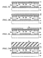
- a sealing film 601 integrated with a projection 601a which corresponds to the structure lower portion.
- the sealing film 601 can be formed as follows. First, a 6- ⁇ m thick resin film is laminated and adhered to the upper electrode 110b by the STP technique, thereby closing the opening portions 110a. After that, as shown in Fig. 6, a region except for a portion corresponding to the structure lower portion is thinned by exposure and development, thereby forming the sealing film 601 having the projection 601a.
- the present invention is not limited to this arrangement.
- the upper portion of the projection 601a of the sealing film 601 can also fit in the lower portion of an upper structure 701, provided that the lower surface of the upper structure 701 is not in contact with a region except for the lower structure of the sealing film 601.
- the support portion forming the lower portion of the structure is made up of one member, but the present invention is not limited to this arrangement.
- the support portion of a structure 801 may also be made up of a plurality of columns 802. Note that the rest of the arrangement shown in Fig. 8 is the same as that shown in Figs. 1A to 1C, so an explanation thereof will be omitted.
- perimeter support portions 902 made of an elastic material can be formed at the four corners of the overhang having a rectangular planar shape of a structure 901 supported by a support portion 901a formed in substantially the center.
- the perimeter support portions 902 can be made of, e.g., rubber or coil springs. The perimeter support portions 902 can prevent a fall of the structure 901.
- the perimeter support portions 902 made of an elastic material elastically deform and crush, and the sealing film 111 and upper electrode 110b are pushed down by the support portion 901a formed in the center. Even when the perimeter support portions 902 are formed as described above, the transmission of the force to the upper electrode 110b by the structure 901 is not inhibited because the perimeter support portions 902 are made of an elastic material.
- a lower electrode 105a, upper electrode 110b, and the like are formed, and the upper electrode 110b is covered with a sealing film 111.
- a seed layer 1001 made of a two-layered film including a 0.1- ⁇ m thick titanium film and 0.1- ⁇ m thick copper film is formed on the sealing film 111 by vapor deposition, sputtering, or the like, and the well-known photolithography technique is used to form a resist pattern 1002 for each sensor element (Fig. 10A).
- the resist pattern 1002 is a pattern having a rectangular planar shape formed in a portion as a structure lower portion (to be described below).
- the resist pattern 1002 is then removed, and the sacrificial film 1003 is used as a mask to remove the seed layer 1001 below the resist pattern 1002, thereby exposing the upper surface of the sealing film 111, above the lower electrode 105a, to an opening portion 1003a as shown in Fig. 10C.
- a photosensitive polyimide film is formed on the sacrificial film 103 and patterned by the photolithography technique, thereby forming a structure lower portion 1004 made of polyimide (resin) as shown in Fig. 10D.
- a seed layer 1005 is so formed as to cover the surfaces of the structure lower portion 1004 and sacrificial film 1003, and a resist pattern 1006 is subsequently formed.
- the seed layer 1005 is a two-layered film including an upper layer made of a 0.1- ⁇ m titanium film and a lower layer made of a 0.1- ⁇ m thick gold film.
- the resist pattern 1006 is a lattice-shaped pattern, and formed in a region where a support member 107a is formed.
- a gold film 1007 about 5 ⁇ m thick is formed on the seed layer 1005 so as to fill the squares of the resist pattern 1006 halfway.
- the gold film 1007 is formed on the exposed seed layer 1005 by plating gold by electroplating.
- the resist pattern 1006 is removed to form a structure upper portion 1008 made of gold in each sensor element.
- the structure upper portion 1008 is used as a mask to remove the seed layer 1005 by wet etching.
- the gold as the upper layer of the seed layer 1005 can be etched by using, e.g., an etchant containing iodine, ammonium iodide, water, and ethanol.
- the titanium as the lower layer of the seed layer 1005 can be etched by using an HF-based etchant. Consequently, the upper surface of the sacrificial film 1003 is exposed around the structure upper portion 1008.
- the sacrificial film 1003 made of copper is etched by an etchant containing nitric acid, and the titanium as the lower layer of the seed layer 1001 is etched by an HF-based etchant, thereby forming a structure made up of the structure lower portion 1004 made of polyimide and the structure upper portion 1008 made of gold.
- This structure has an overhang as the structure upper portion 1008, and the structure lower portion 1004 which supports substantially the center of the structure upper portion 1008.
- the structure is formed in the position of the lower electrode 105a in each sensor chip.
- the overhang of the structure formed on the upper electrode 110b is made of a metal. Therefore, the overhang is a rigid body having a high Young's modulus, does not easily deform, and hardly interferes with deformation of the upper electrode when a fingerprint shape is sensed. Also, when compared to a case in which the overhang is made of a synthetic resin, the rigidity can be ensured even if the thickness is decreased, so the surface shape recognition sensor shown in Fig. 10I can be fabricated within a shorter time period.
- a lower electrode 105a, upper electrode 110b, and the like are formed, and the upper electrode 110b is covered with a sealing film 111.
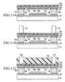
- a 0.1- ⁇ m thick adhesive layer 1101 made of titanium is formed on the sealing film 111 by, e.g., vapor deposition or sputtering, a polyimide layer 1102 is formed on the adhesive layer 1101, and a seed layer 1103 is formed on the polyimide layer 1102 (Fig. 11A).
- the polyimide layer 1102 can be formed by spin coating and thermal cure of a polyimide resin.
- the seed layer 1103 is a two-layered film including a lower layer made of a 0.1- ⁇ m thick titanium film, and an upper layer made of a 0.1- ⁇ m thick gold film.
- the titanium lower layer improves the adhesion to the polyimide layer 1102.
- a resist pattern 1104 is formed on the seed layer 1103 by the well-known photolithography technique.
- the resist pattern 1104 is a lattice-shaped pattern, and formed in a region where a support member 107a is formed.
- a gold film 1105 about 5 ⁇ m thick is formed on the seed layer 1103 so as to fill the square of the resist pattern 1104 halfway.
- the 5- ⁇ m thick gold film 1105 is formed on the exposed seed layer 1103 by plating gold by electroplating.
- the resist pattern 1104 is removed to form a structure upper portion 1106 made of gold in each sensor element.
- the seed layer 1103 is removed by wet etching by using the structure upper portion 1106 as a mask.
- the gold as the upper layer of the seed layer 1103 can be etched by using an etchant containing iodine, ammonium iodide, water, and ethanol.
- the titanium as the lower layer of the seed layer 1103 can be etched by using an HF-based etchant. Consequently, the upper surface of the polyimide layer 1102 is exposed around the structure upper portion 1106.
- a predetermined amount of the polyimide layer 1102 is etched by dry etching using oxygen plasma, thereby forming a structure lower portion 1107 made of polyimide.
- the lower surface of the structure lower portion 1107 is connected and fixed on the sealing film 111 via the adhesive layer 1101, and the upper surface of the structure lower portion 1107 is connected and fixed to the structure upper portion 1106 via the seed layer 1103.
- a structure which is made up of an overhang and a support portion supporting substantially the center of the overhang, and in which the area of the support portion is smaller than the area of the overhang in the two-dimensional direction of an upper electrode is formed on the upper electrode in a region above each lower electrode.
- an object of surface shape sensing e.g., a fingertip touches the surface of the overhang of the structure, and the support portion of this structure whose overhang is in contact with the object of sensing pushes down a portion of the upper electrode toward the lower electrode, thereby deforming the upper electrode.
- This structure can efficiently transmit the force received from the finger to the upper electrode, increase the deflection of the upper electrode, and thereby increase the sensing sensitivity of this sensor.
- the output from the sensor does not largely increase even when the force of pushing the finger increases.
- the sensor output equivalent to that obtained by a hard finger can be obtained by increasing the force which pushes the fingertip.
- the spacing between adjacent structures is narrow, and the upper surface of each structure is a substantially flat surface, so a remarkable effect is obtained by which the sensor does not easily break even if a force is applied sideways by an object of sensing such as a finger, i.e., by which the high mechanical strength is high.
- the surface shape recognition sensor according to the present invention is suited to sensing fingerprints at high accuracy.
Abstract
Description
- The present invention relates to a surface shape recognition sensor used to sense a surface shape having a fine three-dimensional pattern such as a human fingerprint or animal noseprint, and a method of fabricating the same.
- Along with the advance of the information-oriented society and in the environment of the modern society, security technology has received a great deal of attention. For example, in the information-oriented society, personal authentication technology for constructing a system for, e.g., electronic cashing is an important key. Authentication technologies for preventing theft or unauthorized use of credit cards have also been extensively researched and developed. (Reference 1: Yoshimasa Shimizu et al., "A Study on the Structure of a Smart Card with the Function to Verify the Holder", Technical report of IEICE OFS92-32, pp. 25-30 (1992))
- There are various kinds of authentication schemes such as fingerprint authentication and voice authentication. In particular, many fingerprint authentication techniques have been developed so far. Fingerprint reading schemes include an optical scheme which includes an optical system such as a lens and illumination, a pressure scheme using a pressure sheet, and a semiconductor scheme by which a sensor is formed on a semiconductor substrate. Of these schemes, the semiconductor scheme allows easy miniaturization and generalization. An example of the semiconductor sensor is a capacitive fingerprint sensor using LSI fabrication technique. (Reference 2: Marco Tartagni and Robert Guerrieri, "A 390 dpi Live Fingerprint Imager Based of Feedback Capacitive Sensing Scheme", 1997 IEEE International Solid-State Circuits Conference, pp. 200-201 (1997)) This fingerprint sensor senses the three-dimensional pattern of a skin by using the feedback capacitive scheme by a sensor chip in which small capacitive sensors are two-dimensionally arranged on an LSI.
- This capacitive sensor will be described below with reference to a sectional view in Fig. 14. The sensor includes a
sensor electrode 1403 formed on asemiconductor substrate 1401 via an interlevel dielectric 1402, and apassivation film 1404 which covers thesensor electrode 1403. Although not shown in Fig. 14, on thesemiconductor substrate 1401 below the interlevel dielectric 1402, a sensing circuit which is an integrated circuit including a plurality of MOS transistors and an interconnecting structure is formed. When a finger as an object of fingerprint sensing touches the passivation film 1404 (sensing surface) of the sensor chip having the above arrangement, thesensor electrode 1403 and the skin of the finger function as electrodes to form a capacitance. - This capacitance is sensed by the sensing circuit described above via an interconnection (not shown) connected to the
sensor electrode 1403. However, since the capacitive fingerprint sensor uses the skin as an electrode, the built-in integrated circuit of the sensor chip is electrostatically destroyed by the static electricity generated at the fingertip. - To prevent this electrostatic destruction of the capacitive fingerprint sensor described above, a surface shape recognition sensor including a capacitive sensor having a sectional structure as shown in Fig. 15 is proposed. The arrangement of the sensor shown in Fig. 15 will be explained below. This sensor includes a
sensor electrode 1503 formed on asemiconductor substrate 1501 via an interlevel dielectric 1502, a deformable plate-shaped movingelectrode 1504 positioned at a predetermined distance from thesensor electrode 1503, and asupport member 1505 which is formed around thesensor electrode 1503 so as to be insulated and separated from thesensor electrode 1503, and supports the movingelectrode 1504. - When a finger as an object of fingerprint sensing touches the moving
electrode 1504, the pressure from the finger deflects the movingelectrode 1504 toward thesensor electrode 1503, thereby increasing the capacitance formed between thesensor electrode 1503 and movingelectrode 1504. This capacitance is sensed by a sensing circuit on thesemiconductor substrate 1501 via an interconnection (not shown) connected to thesensor electrode 1503. In this surface shape recognition sensor, when the movingelectrode 1504 is grounded via thesupport member 1505, the static electricity generated at the fingertip flows to ground via thesupport member 1505 even if the electricity is discharged to the movingelectrode 1504. This protects the built-in sensing circuit incorporated below thesensor electrode 1503 from the electrostatic destruction. - In addition to the surface shape recognition sensor shown in Fig. 15, a structure having a
cubic projection 1601 as shown in Fig. 16 is also proposed. (Reference 3: Japanese Patent Laid-Open No. 2002-328003) In this structure, forces created byfinger 1602 can be transmitted to the movingelectrode 1504 more efficiently than in the structure shown in Fig. 15. - Unfortunately, the above conventional fingerprint sensors have the problem that no desired high sensitivity can be obtained. For example, in the fingerprint sensor having the arrangement shown in Fig. 14, the sensitivity largely changes in accordance with the state of the finger surface, so it is not easy to stably obtain high sensitivity. Also, in the fingerprint sensor having the arrangement shown in Fig. 15, no large change in upper electrode can be obtained, and this makes it impossible to obtain high sensitivity.
- Furthermore, in the structure shown in Fig. 16, the
projection 1601 is readily damaged by a force applied sideways to the movingelectrode 1504, e.g., a force produced by scratching, and this lowers the mechanical strength. In addition, in the structure shown in Fig. 16, theprojection 1601 sinks into thefinger 1602 if it is soft, and the force disperses in a region on thesupport member 1505 of the movingelectrode 1504, thereby lowering the sensitivity. - The present invention has been made to solve the above problems, and has as its object to provide a surface shape recognition sensor which senses a shape such as a fingerprint at high sensitivity, and has high mechanical strength.
- A surface shape recognition sensor according to the present invention comprises a plurality of capacitance sensing elements comprising a plurality of lower electrodes arranged in the same plane on a substrate so as to be insulated and separated from each other, and a deformable plate-shaped upper electrode formed above the lower electrodes with a predetermined spacing between them, and made of a metal, a support member which is formed around the lower electrode so as to be insulated and separated from the lower electrode, and supports the upper electrode, and a structure formed on the upper electrode in a region above each of the lower electrodes in one-to-one correspondence with the lower electrode, wherein the structure comprises an overhang and a support portion which supports substantially a center of the overhang, and an area of the support portion is smaller than an area of the overhang in a two-dimensional direction of the upper electrode.
- In the surface shape recognition sensor having the above arrangement, an object of surface shape sensing, e.g., a fingertip touches the surface of the overhang of the structure, and the support of the structure whose overhang is in contact with the object of sensing pushes down a portion of the upper electrode toward the lower electrode, thereby deforming the upper electrode.
- The above surface shape recognition sensor may also comprise a thin flexible film formed on the overhang of the structure, and extending over a plurality of the structures, thereby inhibiting an invasion of an object from the gap between adjacent structures. The sensor may also comprise a perimeter support portion formed below a perimeter of the overhang, and made of an elastic material, thereby preventing a fall of the structure.
- In the above surface shape recognition sensor, the substrate may be a semiconductor substrate on which an integrated circuit is formed, the lower electrode may be placed on a interlevel dielectric formed on the semiconductor substrate, and the integrated circuit may include a sensing circuit which senses a capacitance formed on the lower electrode.
- A surface shape recognition sensor fabrication method according to the present invention comprises the steps of forming an interlevel dielectric on a semiconductor substrate, forming a first metal film on the interlevel dielectric, forming a first mask pattern having a first opening portion on the first metal film, forming a first metal pattern by plating on a surface of the first metal film exposed to a bottom of the first opening portion in the first mask pattern, removing the first mask pattern, and forming, on the first metal film and first metal pattern, a second mask pattern having a second opening portion around the first metal pattern, forming a second metal pattern thicker than the first metal pattern by plating on the surface of the first metal pattern exposed to a bottom of the second opening portion in the second mask pattern, removing the second mask pattern, and etching away the first metal film by using the first metal pattern and second metal pattern as masks, thereby forming a lower electrode made of the first metal film and first metal pattern, and a support member made of the first metal film and second metal pattern, forming a first sacrificial film on the interlevel dielectric so as to cover the lower electrode and expose an upper portion of the support member, forming an upper electrode having a plurality of third opening portions on the first sacrificial film and support member, selectively removing the first sacrificial film via the third opening portions after the upper electrode is formed, forming a sealing film on the upper electrode after the first sacrificial film is removed, forming, on the sealing film, a second sacrificial film having a fourth opening portion smaller than an area of a region surrounded by the support member in a region above the lower electrode, forming, on the second sacrificial film, a layer thicker than a depth of the fourth opening portion so as to fill the fourth opening portion, forming a trench in a region, positioned on the support member, of the thick layer, and forming a structure on the sealing film in the region above each of the lower electrodes in one-to-one correspondence with the lower electrode, and removing the second sacrificial film via the trench between adjacent structures, wherein a plurality of capacitance sensing elements comprising the lower electrode and upper electrode are formed.
- In this fabrication method, a structure which includes an overhang and a support portion supporting substantially the center of the overhang, and in which the area of the support portion is smaller than the area of the overhang in the two-dimensional direction of the upper electrode is formed on the upper electrode in the region above each lower electrode.
- In the above surface shape recognition sensor fabrication method, the first sacrificial film may be formed by hot-pressing, on the semiconductor substrate, a dielectric material preformed on a base by coating to bury the dielectric material in the support member and lower electrode, and peeling the base from the dielectric material, thereby forming a thin film having a flat surface on the semiconductor substrate, and exposing the support member by etching back the thin film.
- In the above surface shape recognition sensor fabrication method, the structure may be formed by forming a thin film by coating a bottom of the fourth opening portion and an upper surface of the second sacrificial film with a photosensitive resin, forming the trench by removing a portion of the thin film by exposure and development by using a trench-shaped pattern, and thermally curing the thin film.
- In the above surface shape recognition sensor fabrication method, the step of forming the structure may comprise the steps of forming a second metal film on a bottom of the fourth opening portion and on the second sacrificial film, forming a third mask pattern having an opening portion on the second metal film, forming a third metal pattern by plating on a surface of the second film exposed to a bottom of the third mask pattern, removing the third mask pattern to obtain a portion of the trench, forming the trench by etching away the second metal film exposed to a bottom of the portion of the trench by using the third metal pattern as a mask, and etching away the second sacrificial film via the trench.
- The above surface shape recognition sensor fabrication method may further comprise the steps of forming an etching stop film made of a metal on the sealing film, and forming the second sacrificial film on the etching stop film by using a photosensitive material.
- Another surface shape recognition sensor fabrication method according to the present invention comprises the steps of forming an interlevel dielectric on a semiconductor substrate, forming a first metal film on the interlevel dielectric, forming a first metal pattern by plating on a surface of the first metal film exposed to a bottom of a first opening portion in the first mask pattern, removing the first mask pattern, and forming, on the first metal film and first metal pattern, a second mask pattern having a second opening portion around the first metal pattern, forming a second metal pattern thicker than the first metal pattern by plating on the surface of the first metal pattern exposed to a bottom of the second opening portion in the second mask pattern, removing the second mask pattern, and etching away the first metal film by using the first metal pattern and second metal pattern as masks, thereby forming a lower electrode made of the first metal film and first metal pattern, and a support member made of the first metal film and second metal pattern, forming a first sacrificial film on the interlevel dielectric so as to cover the lower electrode and expose an upper portion of the support member, forming an upper electrode having a plurality of third opening portions on the first sacrificial film and support member, selectively removing the first sacrificial film via the third opening portions after the upper electrode is formed, forming a sealing film on the upper electrode after the first sacrificial film is removed, forming a columnar pattern in a predetermined region on the upper electrode, laminating, on the columnar pattern, a photosensitive resin film separated from the sealing film, and forming a structure made up of the columnar pattern and thin film by removing a portion of the thin film into a shape of a lattice, wherein a plurality of capacitance sensing elements comprising the lower electrode and upper electrode are formed.
- The above surface shape recognition sensor fabrication method may further comprise the step of adhering a thin rubber film on the structure. The method can may further comprise the step of placing a thin film on the structure, and fixing the thin film at an end of a region in which the plurality of capacitance sensing elements are formed.
-
- Fig. 1A is a schematic sectional view showing an example of the arrangement of a surface shape recognition sensor according to an embodiment of the present invention;
- Fig. 1B is a schematic sectional view showing the example of the arrangement of the surface shape recognition sensor according to the embodiment of the present invention;
- Fig. 1C is a perspective view showing the whole structure of the surface shape recognition sensor;
- Figs. 2A to 2P are views of steps for explaining an example of a method of fabricating the surface shape recognition sensor according to the embodiment of the present invention;
- Figs. 3A to 3E are views of steps for explaining another example of the method of fabricating the surface shape recognition sensor according to the embodiment of the present invention;
- Figs. 4A to 4F are views of steps for explaining another example of the method of fabricating the surface shape recognition sensor according to the embodiment of the present invention;
- Figs. 5A to 5D are views of steps for explaining another example of the method of fabricating the surface shape recognition sensor according to the embodiment of the present invention;
- Fig. 6 is a view of a step for explaining another example of the method of fabricating the surface shape recognition sensor according to the embodiment of the present invention;
- Fig. 7 is a view of a step for explaining another example of the method of fabricating the surface shape recognition sensor according to the embodiment of the present invention;
- Fig. 8 is a schematic sectional view showing another example of the arrangement of the surface shape recognition sensor according to the embodiment of the present invention;
- Fig. 9A is a schematic sectional view showing another example of the arrangement of the surface shape recognition sensor according to the embodiment of the present invention;
- Fig. 9B is a plan view schematically showing an example of the arrangement of a portion of the surface shape recognition sensor according to the embodiment of the present invention;
- Figs. 10A to 10I are views of steps for explaining another example of the method of fabricating the surface shape recognition sensor according to the embodiment of the present invention;
- Figs. 11A to 11F are views of steps for explaining another example of the method of fabricating the surface shape recognition sensor according to the embodiment of the present invention;
- Fig. 12 is a graph for explaining the state of sensing by a conventional surface shape recognition sensor;
- Fig. 13 is a graph for explaining the state of sensing by the surface shape recognition sensor according to the embodiment of the present invention;
- Fig. 14 is a schematic sectional view showing an example of the arrangement of a conventional surface shape recognition sensor;
- Fig. 15 is a schematic sectional view showing an example of the arrangement of a conventional surface shape recognition sensor; and
- Fig. 16 is a schematic sectional view showing an example of the arrangement of a conventional surface shape recognition sensor.
- Embodiments of the present invention will be described below with reference to the accompanying drawings.
- First, a surface shape recognition sensor according to the first embodiment of the present invention will be described below with reference to Figs. 1A, 1B, and 1C. Figs. 1A and 1B are schematic sectional views showing an example of the arrangement of this sensor, in which Fig. 1A mainly illustrates a sensor element (sensor cell) 100 as a constituent unit of the surface shape recognition sensor. For example, a plurality of
sensor elements 100 is arranged in a matrix to form the sensing surface of this sensor. Fig. 1B shows the state in which a fingertip as an object of surface shape sensing is in contact with the sensing surface of this sensor. Also, Fig. 1C is a perspective view showing the whole structure of the surface shape recognition sensor. - The arrangement of the
sensor element 100 will be explained in detail below. On asubstrate 101 made of single-crystal silicon or the like, alower electrode 105a is formed via aninterlevel dielectric 102. Thelower electrode 105a is positioned in substantially the center of the region of thesensor element 100. Asupport member 107a is formed around thelower electrode 105a, and anupper electrode 110b is supported on thesupport member 107a. - The
support member 107a is, e.g., a lattice-shape member, and thelower electrode 105a is formed in the center of each square of the lattice. Accordingly, each square of the lattice-shape support member 107a is the region of onesensor element 100. Theupper electrode 110b is integrally formed on thesupport member 107a, so oneupper electrode 110b is formed for a plurality oflower electrodes 105a. Also, theupper electrode 110b is flexible, and a portion opposing thelower electrode 105a is elastically deformable so as to deflect toward thelower electrode 105a. - The
upper electrode 110b has astructure 113b formed on it via asealing film 111. Thestructure 113b is made up of a support portion which is in direct contact with the upper portion of thestructure 113b, and an overhang which extends outward from this support portion. Thestructures 113b adjacent to each other are separated from each other, and, for example, eachstructure 113b is paired with thelower electrode 105a. As is also shown in Fig. 1B, thestructure 113b is formed in eachsensor element 100. - The overhang of the
structure 113b is formed so as not to exceed the region of thesensor element 100 in the direction in which theupper electrode 110b runs. By contrast, the support portion of thestructure 113b is made as small as possible so as to be able to support the overhang. - The overhang of the
structure 113b need only have a substantially square planar shape. For example, when thesensor elements 100 are arranged at an interval of 50 µm, it is only necessary to form the overhang of thestructure 113b as a square of 45 µm side, and form the support portion in contact with the sealingfilm 111 as a square of 5 µm side. - In this surface shape recognition sensor, as shown in Fig. 1B, the
upper electrode 110b below thestructure 113b which is pushed down when touched by afinger 1602 deflects downward, and this changes the capacitance formed by theupper electrode 110b andlower electrode 105a. In this state, a downward pushing force is applied to the overhang having a large area of thestructure 113b, and this force is transmitted to theupper electrode 110b via the support portion having a small area of thestructure 113b. Accordingly, force applied per unit area increases in theupper electrode 110b. - In this embodiment as described above, the force applied to substantially the entire area of the
sensor element 100 when thefinger 1602 touches is concentrated to the support portion of thestructure 113b and transmitted to theupper electrode 110b. In this embodiment, therefore, the sensitivity of the surface shape recognition sensor can be increased. Also, in this embodiment, the spacing between theadjacent structures 113b is narrow, so it is possible to prevent thestructure 113b from sinking into thefinger 1602 to disperse the force. - The operation of the this surface shape recognition sensor will be briefly explained below. When a finger touches the sensing surface on which the plurality of
structures 113b are arranged, and pushes onestructure 113b downward, theupper electrode 110b of thesensor element 100 below thestructure 113b that is pushed down deflects downward. This deflection changes the capacitance formed between theupper electrode 110b and lower electrode. The shape of the fingerprint can be regenerated by forming continuous tone data in accordance with those changes in capacitances formed on thelower electrodes 105a, which correspond to the fingerprint shape. - Note that the sensing of the capacitance in each sensor cell when the
upper electrode 110b deforms and the conversion into the continuous tone data are performed by, e.g., an integrated circuit (not shown) formed on thesubstrate 101. Note also that when, for example, theupper electrode 110b is grounded, static electricity generated in an object flows to ground even if this static electricity is discharged to theupper electrode 110b. By thus connecting theupper electrode 110b to ground, the integrated circuit can be protected from electrostatic destruction. - A method of fabricating the surface shape recognition sensor according to this embodiment described above will be explained below. First, as shown in Fig. 2A, an
interlevel dielectric 102 made of silicon nitride or the like is formed on asubstrate 101 made of a semiconductor material such as silicon. Although not shown, an integrated circuit such as a sensing circuit and an interconnecting structure having a plurality of interconnections are formed on thesubstrate 101 below theinterlevel dielectric 102. After theinterlevel dielectric 102 is formed, a seed layer (first metal film) 103 which is a two-layered film made up of a 0.1-µm thick titanium film and 0.1-µm thick gold film is formed by vapor deposition or the like. Note that theinterlevel dielectric 102 may also be made of silicon oxide, but it is preferably made of silicon nitride when an HF-based etching process (to be described later) is taken into consideration. - Subsequently, as shown in Fig. 2B, a resist pattern (first mask pattern) 104 about 5 µm thick having an
opening portion 104a is formed on theseed layer 103. The resistpattern 104 is formed by the well-known photolithography technique. When the resistpattern 104 is formed, a metal pattern (first metal pattern) 105 about 1 µm thick made of a gold plating film is formed by electroplating on theseed layer 103 exposed to theopening portion 104a. Since the film is formed by electroplating, the gold plating film is not formed on the resistpattern 104, and themetal pattern 105 is selectively formed on theseed layer 103 exposed to theopening portion 104a. - After the resist
pattern 104 is removed, as shown in Fig. 2C, a 5-µm thick resist pattern (second mask pattern) 106 having anopening portion 106a is formed. The resistpattern 106 is formed so that it covers themetal pattern 105 and theopening portion 106a is positioned in a prospective region of thesupport member 107a shown in Fig. 1. After the resistpattern 106 is formed, a metal pattern (second metal pattern) 107 about 3 µm thick made of a gold plating film is formed by electroplating on theseed layer 103 exposed to theopening portion 106a. - After the resist
pattern 106 is removed, themetal patterns seed layer 103. In this etching, an etchant containing iodine, ammonium iodide, water, and ethanol is first used to selectively remove the gold as the upper layer of theseed layer 103. Then, an HF-based etchant is used to selectively remove the titanium as the lower layer of theseed layer 103. Note that the etching rate in the gold wet etching is 0.05 µm/min. - Consequently, as shown in Fig. 2E, a
lower electrode 105a having the gold upper layer and asupport member 107a insulated and separated from thelower electrode 105a are formed on thesubstrate 101. As shown in Fig. 1, thesupport member 107a supports theupper electrode 110b. Also, as shown in the plan view of Fig. 2D, thesupport member 107a is formed into the shape of a lattice on thesubstrate 101. A plurality oflower electrodes 105a is arranged in the centers of regions surrounded by the lattice-shapedsupport member 107a. - When the
lower electrode 105a andsupport member 107a are formed as described above, as shown in Fig. 2E, a sacrificial film 108 (first sacrificial film) is so formed as to cover thelower electrode 105a and expose the upper surface of thesupport member 107a. The formation of thesacrificial film 108 will be briefly explained below. First, a photosensitive resin film is formed on thesubstrate 101 by spin coating, thereby covering thelower electrode 105a andsupport member 107a. The resin film has positive photosensitivity, and is formed by, e.g., adding a positive photosensitive agent to a base resin (polyimide) such as polyamide, polyamide acid, or polybenzoxazole (or its precursor). - After a heating process (prebaking) is performed, the region above the
support member 107a is exposed by using the well-known photolithography technique, and development is subsequently performed to expose the upper portion of thesupport member 107a. After that, the resin film is cured by a heating process and etched back by chemical mechanical polishing, thereby substantially leveling thesupport member 107a andsacrificial film 108 with each other as shown in Fig. 2E. - After the
sacrificial film 108 is formed as described above, as shown in Fig. 2F, on thesacrificial film 108 in which the upper surface of thesupport member 107a is exposed by planarization, aseed layer 109 which is a two-layered film made up of a 0.1-µm thick titanium film and 0.1-µm thick gold film is formed by vapor deposition or the like. - Then, as shown in Fig. 2G, a columnar resist
pattern 201 is formed on theseed layer 109, and ametal film 110 about 1.0 µm thick made of a gold plating film is formed by electroplating on the exposedseed layer 109 in a region where the resistpattern 201 is not formed. - After the resist
pattern 201 is removed, the formedmetal film 110 is used as a mask to selectively etch away theseed layer 109. Consequently, as shown in Fig. 2H, anupper electrode 110b having a plurality of openingportions 110a is formed. The openingportions 110a have a square planar shape of 4 µm side, and are arranged at the four corners inside thesupport member 107a. - Subsequently, as shown in Fig. 2I, the
sacrificial film 108 is removed via the openingportions 110a in theupper electrode 110b to form a space below theupper electrode 110b. With the formed space sandwiched between them, the upper surface of thelower electrode 105a opposes the lower surface of theupper electrode 110 at a predetermined distance. Note that theupper electrode 110b is supported by thesupport member 107a. Note also that thesacrificial film 108 is removed by exposing thesubstrate 101 to a plasma mainly containing oxygen gas, and bringing the etching species generated by the plasma into contact with thesacrificial film 108 via the openingportions 110a. - As shown in Fig. 2J, a sealing
film 111 is laminated and adhered to theupper electrode 110b to close the openingportions 110a while the space between theupper electrode 110b andlower electrode 105a is held. The formation of the sealingfilm 111 by lamination was performed by using an STP technique (Spin-coating film Transfer and hot-Pressing technique). This technique will be briefly explained below. First, a resin film preformed on a sheet film by coating is hot-pressed on theupper electrode 110b in a vacuum. Then, the sheet film is peeled from the resin film, and the resin film laminated on theupper electrode 110b is cured by a heat treatment which holds the temperature at 300°C for about 1 hr. As a consequence, the sealingfilm 111 made of the resin film is formed on theupper electrode 110b. The resin film is made of a base resin (polyimide) such as polyamide, polyamide acid, or polybenzoxazole (or its precursor). - After the
sealing film 111 is formed as described above, as shown in Fig. 2K, asilicon oxide film 112 about 1.5 µm thick is deposited on thesealing film 111 by sputtering. Then, a resist pattern about 3 µm thick having a square opening portion of about 5 µm side in substantially the center of theupper electrode 110b is formed by the well-know photolithography technique. Thesilicon oxide film 112 on the bottom of the opening portion in this resist pattern is etched away by ah HF-based etchant, and the resist pattern is removed after that. Consequently, as shown in Fig. 2L, asacrificial film 112b (second sacrificial film) made of the silicon oxide film and having anopening portion 112a is formed. - As will be explained below, the
opening portion 112a in thesacrificial film 112b is a mold for forming a support portion for supporting thestructure 113b. Therefore, theopening portion 112a is formed to have an area smaller than at least the element region surrounded by thesupport member 107a, preferably, smaller than thelower electrode 105a. Also, theopening portion 112a is positioned in the region above substantially the center of thelower electrode 105a. The depth of theopening portion 112a is the height of the support portion of thestructure 113b. Accordingly, the thickness of thesacrificial film 112b is appropriately set in accordance with the shape of the desiredstructure 113b. - As shown in Fig. 2M, a
photosensitive resin film 113 about 10 µm thick is formed by spin coating on thesacrificial film 112b and sealingfilm 111. The resin film has positive photosensitivity, and is formed by, e.g., adding a positive photosensitive agent to a base resin (polyimide) such as polyamide, polyamide acid, or polybenzoxazole (or its precursor). - After the
resin film 113 is formed by coating and heated (prebaked), a region substantially corresponding to the upper portion of thesupport member 107a is exposed by the well-known photolithography technique. As shown in Fig. 2N, development is subsequently performed to formtrenches 113a and astructure 113b. The width of thetrench 113a is about 5 µm. After that, thestructure 113b is cured by a heating process by which it is held at about 300°C for 1 hr. - The
sacrificial film 112b is then etched away by allowing an HF-based etchant to act from thetrenches 113a. Consequently, as shown in Fig. 20, thestructure 113b is given a support portion which is in direct contact with the upper surface of the sealingfilm 111, and an overhang which extends outward from this support portion. Thestructure 113b has a T-shaped section, and the area of the uppermost portion is larger than the portion adhered to thesealing film 111. Also, thestructures 113b are formed in one-to-one correspondence with thelower electrodes 105a, and the overhangs ofadjacent structures 113b are separated by about 5 µm. - In this embodiment, the lower portion (support portion) of the
structure 113b is narrower than its upper portion (overhang), and adhered to substantially the center of theupper electrode 110b. Also, the thickness of theupper electrode 110b positioned immediately below the adhered portion between thestructure 113b and sealingfilm 111 apparently increases by the presence of thestructure 113b, so theupper electrode 110b does not easily deflect. However, theupper electrode 110b around the adhered portion has the thickness of theupper electrode 110b and sealingfilm 111, and easily deflects. - The adhered portion between the
structure 113b and sealingfilm 111 is positioned in the center of theupper electrode 110b, and the deflection of theupper electrode 110b is a maximum in this portion. Therefore, thestructure 113b efficiently transmits a force received from a finger to theupper electrode 110b, and this makes it possible to increase the deflection of theupper electrode 110b. - Note that in the above embodiment a silicon oxide film is used as the second sacrificial film (
sacrificial film 112b) and an HF-based etchant is used as the etchant for the film, but the present invention is not limited to this embodiment. It is also possible to from the second sacrificial film from titanium, and remove the film by an HF-based etchant. Alternatively, it is possible to form the second sacrificial film from a copper film obtained by plating, and remove the film by an etchant containing nitric acid or the like. - Furthermore, the
sacrificial film 108 is formed by forming a photosensitive resin film by spin coating and forming a flat surface by etching back the film by chemical mechanical polishing, but it is also possible to form a flat surface by filling thesupport member 107a andlower electrode 105a with a photosensitive film by the STP technique without using any chemical mechanical polishing, and exposing thesupport member 107a by etching back as needed. - In addition to the above structure, as shown in Fig. 2P, a
thin film 120 may also be formed on thestructure 113b. As thethin film 120, a resin film about 2 µm thick, for example, can be adhered on the upper surface of thestructure 113b by using the STP technique. It is also possible to adhere rubber about 10 µm thick on the upper surface of thestructure 113b. This prevents a portion of an object from entering thetrenches 113a around thestructure 113b. Also, since the film is made of rubber, thestructures 113b adjacent to each other do not completely interlock with each other, but can move independently of each other. - Alternatively, a film about 10 µm thick made of an organic material can be formed as the
thin film 120, and fixed at the end portions of the sensing surface on which the plurality ofstructures 113b are arranged. In this structure, thetrenches 113a are completely closed from the outside, and the film is not adhered to the upper surface of thestructure 113b, so thestructures 113b adjacent to each other can move independently of each other. - Another embodiment of the present invention will be described below.
- First, following the same procedures as in Figs. 2A to 2J, a
lower electrode 105a,upper electrode 110b, and the like are formed, and theupper electrode 110b is covered with asealing film 111. - Subsequently, a silicon oxide film is formed on the
sealing film 111 by sputtering or the like, and patterned by the well-know photolithography technique or the like, thereby forming a sacrificial film 301 (second sacrificial film) having anopening portion 301a as shown in Fig. 3A. - After the
sacrificial film 301 is formed as described above, as shown in Fig. 3B, a seed layer (second metal film) 302 which is a two-layered film including a 0.1-µm thick chromium film and 0.1-µm thick gold film is formed by vapor deposition or the like. Then, as shown in Fig. 3C, a resist pattern 303 (third mask pattern) is formed. The resistpattern 303 is a lattice-shaped pattern, and formed in a region where asupport member 107a is formed. - In addition, to fill the squares of the resist
pattern 303 halfway, a metal pattern (third metal pattern) 304 about 10 µm thick is formed on theseed layer 302. Themetal pattern 304 need only be selectively formed on the exposedseed layer 302 by electroplating. - When the resist
pattern 303 is removed after themetal pattern 304 is formed as described above, ametal pattern 304 havingopening portions 304a is formed as shown in Fig. 3D. - After that, the
metal pattern 304 is used as a mask to selectively etch theseed layer 302 exposed to the bottoms of the openingportions 304a. In this etching, an etchant containing iodine, ammonium iodide, water, and ethanol is first used to selectively remove the gold as the upper layer of theseed layer 302. Then, an etchant containing potassium ferricyanide and sodium hydroxide is used to selectively remove the chromium as the lower layer of the seed layer 302 (Fig. 3D). - Subsequently, the
sacrificial film 301 is etched away via the openingportions 304a. In this etching, an HF-based etchant was used. Consequently, as shown in Fig. 3E, a structure made of themetal pattern 304 and having an upper portion larger than a lower portion is formed. - In this embodiment, a silicon oxide film is used as the second sacrificial film, and an HF-based etchant is used as the etchant for this film, but the present invention is not limited to this embodiment. For example, it is also possible to form the second sacrificial film from titanium, and remove the film by using an HF-based etchant.
- The following method is also possible. A 0.2-µm thick titanium film 401 (etching stop film) is formed on the
sealing film 111 by vapor deposition (Fig. 4A). After that, a secondsacrificial film 402 made of a resin film is formed by coating, and anopening portion 402a is formed by the well-known photolithography technique. Thesacrificial film 402 has positive photosensitivity, and is formed by, e.g., adding a positive photosensitive agent to a base resin (polyimide) such as polyamide, polyamide acid, or polybenzoxazole (or its precursor). - Then, a seed layer 403 (second metal film) made of a two-layered film including a 0.1-µm thick titanium film and 0.1-µm thick gold film is formed by vapor deposition or the like (Fig. 4B). As shown in Fig. 4C, a frame-shaped resist
pattern 404 is formed and used as a mask pattern to form a gold plating film about 10 µm thick on theseed layer 403 by electroplating. When the resistpattern 404 is removed after that, as shown in Fig. 4D, a metal pattern 405 (third metal pattern) having opening portions in portions from which the resistpattern 404 is removed is formed. - After that, the
metal pattern 405 is used as a mask to selectively etch away theseed layer 403. Thesubstrate 101 is then exposed to a plasma mainly containing oxygen gas, and the etching species generated by the plasma is brought into contact with thesacrificial film 402, thereby removing the sacrificial film 402 (Fig. 4E). In this manner, ametal pattern 405 which is a structure having an upper portion larger than a lower portion is formed. - If necessary, as shown in Fig. 4F, it is also possible to remove a portion of the
titanium film 401 on thesealing film 111 or to remove the titanium film as the lower layer of theseed layer 403 by using an HF-based etchant, thereby exposing the surface of the sealingfilm 111. - Another embodiment of the present invention will be described below.
- First, following the same procedures as in Figs. 2A to 2J, a
lower electrode 105a,upper electrode 110b, and the like are formed, and theupper electrode 110b is covered with a sealing film 111 (Fig. 5A). - Subsequently, as shown in Fig. 5B, a structure lower portion 501 (columnar pattern) is formed by a resin film on the
sealing film 111. The structurelower portion 501 has a substantially square planar shape of about 5 µm side. The resin film has positive photosensitivity, and is formed by, e.g., adding a positive photosensitive agent to a base resin (polyimide) such as polyamide, polyamide acid, or polybenzoxazole (or its precursor). - After this resin film about 5 µm thick is formed on the
sealing film 111 by spin coating, as shown in Fig. 5B, the well-known photolithography technique is used to remove the resin film by exposure and development from a region except for a square region of about 5 µm side on a central portion of theupper electrode 110b. After that, the resin film is cured by performing heat treatment at about 300°C for 1 hr, thereby forming a structurelower portion 501 made of the resin film. - Then, a
resin film 502 is laminated by hot-pressing by using the STP technique. Theresin film 502 has positive photosensitivity, and is formed by, e.g., adding a positive photosensitive agent to a base resin (polyimide) such as polyamide, polyamide acid, or polybenzoxazole (or its precursor). In this lamination, the resin film formed on a sheet film by coating is hot-pressed and laminated on the structurelower portion 501 such that the resin film comes in contact with the structurelower portion 501 and does not contact the sealingfilm 111. After that, as shown in Fig. 5C, only the sheet film is peeled off to form aresin film 502. - After the
resin film 502 is formed as described above, theresin film 502 is patterned using the well-known photolithography technique. In this patterning, theresin film 502 on the upper perimeter of asupport member 107a is exposed by a frame-shaped pattern and developed. By this patterning, as shown in Fig. 5D, openingportions 502a and a structureupper portion 502b are formed. After that, the structureupper portion 502b having the openingportions 502a is cured by a heating process which holds the temperature at about 300°C for 1 hr, thereby forming astructure 503 made up of the structurelower portion 501 and structureupper portion 502b. - In this embodiment explained with reference to Figs. 5A to 5D, the STP technique is used to form the structure having the upper portion larger than the lower portion. Therefore, this embodiment eliminates the step of forming and etching away a sacrificial film, and makes it possible to reduce the number of steps of fabricating the surface shape recognition sensor.
- In this embodiment, as shown in Fig. 5A, a film having a uniform film thickness is used as the sealing
film 111, but the present invention is not limited to this embodiment. For example, as shown in Fig. 6, it is also possible to use asealing film 601 integrated with aprojection 601a which corresponds to the structure lower portion. - The sealing
film 601 can be formed as follows. First, a 6-µm thick resin film is laminated and adhered to theupper electrode 110b by the STP technique, thereby closing the openingportions 110a. After that, as shown in Fig. 6, a region except for a portion corresponding to the structure lower portion is thinned by exposure and development, thereby forming the sealingfilm 601 having theprojection 601a. - Although in Fig. 5D the
resin film 502 is formed in contact with the upper surface of the structurelower portion 501, the present invention is not limited to this arrangement. - For example, as shown in Fig. 7, the upper portion of the
projection 601a of the sealingfilm 601 can also fit in the lower portion of anupper structure 701, provided that the lower surface of theupper structure 701 is not in contact with a region except for the lower structure of the sealingfilm 601. - In the above description, the support portion forming the lower portion of the structure is made up of one member, but the present invention is not limited to this arrangement. For example, as shown in Fig. 8, the support portion of a
structure 801 may also be made up of a plurality ofcolumns 802. Note that the rest of the arrangement shown in Fig. 8 is the same as that shown in Figs. 1A to 1C, so an explanation thereof will be omitted. - Also, the overhang as the upper portion of the structure is supported by the support portion formed in substantially the center of the overhang as described above, but the present invention is not limited to this arrangement. As shown in Figs. 9A and 9B,
perimeter support portions 902 made of an elastic material can be formed at the four corners of the overhang having a rectangular planar shape of astructure 901 supported by asupport portion 901a formed in substantially the center. Theperimeter support portions 902 can be made of, e.g., rubber or coil springs. Theperimeter support portions 902 can prevent a fall of thestructure 901. - When the
structure 901 is pushed down toward thelower electrode 105a, theperimeter support portions 902 made of an elastic material elastically deform and crush, and thesealing film 111 andupper electrode 110b are pushed down by thesupport portion 901a formed in the center. Even when theperimeter support portions 902 are formed as described above, the transmission of the force to theupper electrode 110b by thestructure 901 is not inhibited because theperimeter support portions 902 are made of an elastic material. - An arrangement in which the support portion as the structure lower portion and the overhang as the structure upper portion are made of different materials will be explained below.
- First, following the same procedures as in Figs. 2A to 2J, a
lower electrode 105a,upper electrode 110b, and the like are formed, and theupper electrode 110b is covered with asealing film 111. Subsequently, aseed layer 1001 made of a two-layered film including a 0.1-µm thick titanium film and 0.1-µm thick copper film is formed on thesealing film 111 by vapor deposition, sputtering, or the like, and the well-known photolithography technique is used to form a resistpattern 1002 for each sensor element (Fig. 10A). The resistpattern 1002 is a pattern having a rectangular planar shape formed in a portion as a structure lower portion (to be described below). - As shown in Fig. 10B, copper is deposited by electroplating on the
seed layer 1001 exposed around the resistpattern 1002, thereby forming a coppersacrificial film 1003. - The resist
pattern 1002 is then removed, and thesacrificial film 1003 is used as a mask to remove theseed layer 1001 below the resistpattern 1002, thereby exposing the upper surface of the sealingfilm 111, above thelower electrode 105a, to anopening portion 1003a as shown in Fig. 10C. - Then, a photosensitive polyimide film is formed on the
sacrificial film 103 and patterned by the photolithography technique, thereby forming a structurelower portion 1004 made of polyimide (resin) as shown in Fig. 10D. - As shown in Fig. 10E, a
seed layer 1005 is so formed as to cover the surfaces of the structurelower portion 1004 andsacrificial film 1003, and a resistpattern 1006 is subsequently formed. Theseed layer 1005 is a two-layered film including an upper layer made of a 0.1-µm titanium film and a lower layer made of a 0.1-µm thick gold film. Also, the resistpattern 1006 is a lattice-shaped pattern, and formed in a region where asupport member 107a is formed. - As shown in Fig. 10F, a
gold film 1007 about 5 µm thick is formed on theseed layer 1005 so as to fill the squares of the resistpattern 1006 halfway. Thegold film 1007 is formed on the exposedseed layer 1005 by plating gold by electroplating. - After that, as shown in Fig. 10G, the resist
pattern 1006 is removed to form a structureupper portion 1008 made of gold in each sensor element. - As shown in Fig. 10H, the structure
upper portion 1008 is used as a mask to remove theseed layer 1005 by wet etching. For example, the gold as the upper layer of theseed layer 1005 can be etched by using, e.g., an etchant containing iodine, ammonium iodide, water, and ethanol. Also, the titanium as the lower layer of theseed layer 1005 can be etched by using an HF-based etchant. Consequently, the upper surface of thesacrificial film 1003 is exposed around the structureupper portion 1008. - Finally, as shown in Fig. 10I, in the region exposed around the structure
upper portion 1008, thesacrificial film 1003 made of copper is etched by an etchant containing nitric acid, and the titanium as the lower layer of theseed layer 1001 is etched by an HF-based etchant, thereby forming a structure made up of the structurelower portion 1004 made of polyimide and the structureupper portion 1008 made of gold. This structure has an overhang as the structureupper portion 1008, and the structurelower portion 1004 which supports substantially the center of the structureupper portion 1008. The structure is formed in the position of thelower electrode 105a in each sensor chip. - In the surface shape recognition sensor shown in Fig. 10I, the overhang of the structure formed on the
upper electrode 110b is made of a metal. Therefore, the overhang is a rigid body having a high Young's modulus, does not easily deform, and hardly interferes with deformation of the upper electrode when a fingerprint shape is sensed. Also, when compared to a case in which the overhang is made of a synthetic resin, the rigidity can be ensured even if the thickness is decreased, so the surface shape recognition sensor shown in Fig. 10I can be fabricated within a shorter time period. - Another example of the arrangement in which the support portion as the structure lower portion and the overhang as the structure upper portion are made of different materials will be explained below.
- Following the same procedures as in Figs. 2A to 2J, a
lower electrode 105a,upper electrode 110b, and the like are formed, and theupper electrode 110b is covered with asealing film 111. Subsequently, a 0.1-µmthick adhesive layer 1101 made of titanium is formed on thesealing film 111 by, e.g., vapor deposition or sputtering, apolyimide layer 1102 is formed on theadhesive layer 1101, and aseed layer 1103 is formed on the polyimide layer 1102 (Fig. 11A). Thepolyimide layer 1102 can be formed by spin coating and thermal cure of a polyimide resin. Also, theseed layer 1103 is a two-layered film including a lower layer made of a 0.1-µm thick titanium film, and an upper layer made of a 0.1-µm thick gold film. In theseed layer 1103, the titanium lower layer improves the adhesion to thepolyimide layer 1102. - Subsequently, as shown in Fig. 11B, a resist
pattern 1104 is formed on theseed layer 1103 by the well-known photolithography technique. The resistpattern 1104 is a lattice-shaped pattern, and formed in a region where asupport member 107a is formed. - As shown in Fig. 11C, a
gold film 1105 about 5 µm thick is formed on theseed layer 1103 so as to fill the square of the resistpattern 1104 halfway. The 5-µmthick gold film 1105 is formed on the exposedseed layer 1103 by plating gold by electroplating. - After that, as shown in Fig. 11D, the resist
pattern 1104 is removed to form a structureupper portion 1106 made of gold in each sensor element. Also, theseed layer 1103 is removed by wet etching by using the structureupper portion 1106 as a mask. For example, the gold as the upper layer of theseed layer 1103 can be etched by using an etchant containing iodine, ammonium iodide, water, and ethanol. Also, the titanium as the lower layer of theseed layer 1103 can be etched by using an HF-based etchant. Consequently, the upper surface of thepolyimide layer 1102 is exposed around the structureupper portion 1106. - Finally, as shown in Fig. 11E, in the region exposed around the structure
upper portion 1106, a predetermined amount of thepolyimide layer 1102 is etched by dry etching using oxygen plasma, thereby forming a structurelower portion 1107 made of polyimide. In this state, the lower surface of the structurelower portion 1107 is connected and fixed on thesealing film 111 via theadhesive layer 1101, and the upper surface of the structurelower portion 1107 is connected and fixed to the structureupper portion 1106 via theseed layer 1103. - Note that as shown in Fig. 11F, it is also possible to remove portions other than the
adhesive layer 1101 andseed layer 1103 in contact with the structurelower portion 1107 by wet etching. - In the present invention as has been explained above, a structure which is made up of an overhang and a support portion supporting substantially the center of the overhang, and in which the area of the support portion is smaller than the area of the overhang in the two-dimensional direction of an upper electrode is formed on the upper electrode in a region above each lower electrode. In a surface shape recognition sensor having this arrangement, an object of surface shape sensing, e.g., a fingertip touches the surface of the overhang of the structure, and the support portion of this structure whose overhang is in contact with the object of sensing pushes down a portion of the upper electrode toward the lower electrode, thereby deforming the upper electrode.
- This structure can efficiently transmit the force received from the finger to the upper electrode, increase the deflection of the upper electrode, and thereby increase the sensing sensitivity of this sensor.
- For example, as shown in Fig. 12, in the conventional structure having no overhang, if the surface of a finger as an object of fingerprint sensing is soft, the output from the sensor does not largely increase even when the force of pushing the finger increases. By contrast, in the arrangement of the present invention having the overhang, even if the surface of a finger is soft, the sensor output equivalent to that obtained by a hard finger can be obtained by increasing the force which pushes the fingertip.
- Also, in the arrangement of the present invention, the spacing between adjacent structures is narrow, and the upper surface of each structure is a substantially flat surface, so a remarkable effect is obtained by which the sensor does not easily break even if a force is applied sideways by an object of sensing such as a finger, i.e., by which the high mechanical strength is high.
- As described above, the surface shape recognition sensor according to the present invention is suited to sensing fingerprints at high accuracy.
Claims (12)
- A surface shape recognition sensor characterized by comprising:a plurality of capacitance sensing elements comprising a plurality of lower electrodes arranged in the same plane on a substrate so as to be insulated and separated from each other, and a deformable plate-shaped upper electrode formed above said lower electrodes with a predetermined spacing therebetween, and made of a metal;a support member which is formed around said lower electrode so as to be insulated and separated from said lower electrode, and supports said upper electrode; anda structure formed on said upper electrode in a region above each of said lower electrodes in one-to-one correspondence with said lower electrode,wherein said structure comprises an overhang and a support portion which supports substantially a center of said overhang, and
an area of said support portion is smaller than an area of said overhang in a two-dimensional direction of said upper electrode. - A surface shape recognition sensor according to claim 1, characterized by further comprising a thin flexible film formed on said overhang of said structure, and extending over a plurality of said structures.
- A surface shape recognition sensor according to claim 1, characterized by further comprising a perimeter support portion formed below a perimeter of said overhang, and made of an elastic material.
- A surface shape recognition sensor according to claim 1, characterized in that
said substrate is a semiconductor substrate on which an integrated circuit is formed,
said lower electrode is placed on a interlevel dielectric formed on said semiconductor substrate, and
said integrated circuit includes a sensing circuit which senses a capacitance formed on said lower electrode. - A surface shape recognition sensor fabrication method comprising the steps of:forming an interlevel dielectric on a semiconductor substrate;forming a first metal film on the interlevel dielectric;forming a first mask pattern having a first opening portion on the first metal film;forming a first metal pattern by plating on a surface of the first metal film exposed to a bottom of the first opening portion in the first mask pattern;removing the first mask pattern, and forming, on the first metal film and first metal pattern, a second mask pattern having a second opening portion around the first metal pattern;forming a second metal pattern thicker than the first metal pattern by plating on the surface of the first metal pattern exposed to a bottom of the second opening portion in the second mask pattern;removing the second mask pattern, and etching away the first metal film by using the first metal pattern and second metal pattern as masks, thereby forming a lower electrode made of the first metal film and first metal pattern, and a support member made of the first metal film and second metal pattern;forming a first sacrificial film on the interlevel dielectric so as to cover the lower electrode and expose an upper portion of the support member;forming an upper electrode having a plurality of third opening portions on the first sacrificial film and support member;selectively removing the first sacrificial film via the third opening portions after the upper electrode is formed;forming a sealing film on the upper electrode after the first sacrificial film is removed;forming, on the sealing film, a second sacrificial film having a fourth opening portion smaller than an area of a region surrounded by the support member in a region above the lower electrode;forming, on the second sacrificial film, a layer thicker than a depth of the fourth opening portion so as to fill the fourth opening portion;forming a trench in a region, positioned on the support member, of the thick layer, and forming a structure on the sealing film in the region above each of the lower electrodes in one-to-one correspondence with the lower electrode; andremoving the second sacrificial film via the trench between adjacent structures,wherein a plurality of capacitance sensing elements comprising the lower electrode and upper electrode are formed.
- A surface shape recognition sensor fabrication method according to claim 5, characterized in that
the first sacrificial film is formed by
hot-pressing, on the semiconductor substrate, a dielectric material preformed on a base by coating to bury the dielectric material in the support member and lower electrode, and peeling the base from the dielectric material, thereby forming a thin film having a flat surface on the semiconductor substrate, and
exposing the support member by etching back the thin film. - A surface shape recognition sensor fabrication method according to claim 5, characterized in that the structure is formed by forming a thin film by coating a bottom of the fourth opening portion and an upper surface of the second sacrificial film with a photosensitive resin, forming the trench by removing a portion of the thin film by exposure and development by using a trench-shaped pattern, and thermally curing the thin film.
- A surface shape recognition sensor fabrication method according to claim 5, characterized in that the step of forming the structure comprises the steps of:forming a second metal film on a bottom of the fourth opening portion and on the second sacrificial film;forming a third mask pattern having an opening portion on the second metal film;forming a third metal pattern by plating on a surface of the second film exposed to a bottom of the third mask pattern;removing the third mask pattern to obtain a portion of the trench;forming the trench by etching away the second metal film exposed to a bottom of the portion of the trench by using the third metal pattern as a mask; andetching away the second sacrificial film via the trench.
- A surface shape recognition sensor fabrication method according to claim 5, characterized by further comprising the steps of:forming an etching stop film made of a metal on the sealing film; andforming the second sacrificial film on the etching stop film by using a photosensitive material.
- A surface shape recognition sensor fabrication method comprising the steps of:forming an interlevel dielectric on a semiconductor substrate;forming a first metal film on the interlevel dielectric;forming a first metal pattern by plating on a surface of the first metal film exposed to a bottom of a first opening portion in the first mask pattern;removing the first mask pattern, and forming, on the first metal film and first metal pattern, a second mask pattern having a second opening portion around the first metal pattern;forming a second metal pattern thicker than the first metal pattern by plating on the surface of the first metal pattern exposed to a bottom of the second opening portion in the second mask pattern;removing the second mask pattern, and etching away the first metal film by using the first metal pattern and second metal pattern as masks, thereby forming a lower electrode made of the first metal film and first metal pattern, and a support member made of the first metal film and second metal pattern;forming a first sacrificial film on the interlevel dielectric so as to cover the lower electrode and expose an upper portion of the support member;forming an upper electrode having a plurality of third opening portions on the first sacrificial film and support member;selectively removing the first sacrificial film via the third opening portions after the upper electrode is formed;forming a sealing film on the upper electrode after the first sacrificial film is removed;forming a columnar pattern in a predetermined region on the upper electrode;laminating, on the columnar pattern, a photosensitive resin film separated from the sealing film; andforming a structure made up of the columnar pattern and thin film by removing a portion of the thin film into a shape of a lattice,wherein a plurality of capacitance sensing elements comprising the lower electrode and upper electrode are formed.
- A surface shape recognition sensor fabrication method according to claim 5, characterized by further comprising the step of adhering a thin rubber film on the structure.
- A surface shape recognition sensor fabrication method according to claim 5, characterized by further comprising the step of placing a thin film on the structure, and fixing the thin film at an end of a region in which the plurality of capacitance sensing elements are formed.
Applications Claiming Priority (3)
| Application Number | Priority Date | Filing Date | Title |
|---|---|---|---|
| JP2003038915 | 2003-02-17 | ||
| JP2003038915 | 2003-02-17 | ||
| PCT/JP2004/001532 WO2004072576A1 (en) | 2003-02-17 | 2004-02-13 | Surface shape recognition sensor and method of producing the same |
Publications (2)
| Publication Number | Publication Date |
|---|---|
| EP1491852A1 true EP1491852A1 (en) | 2004-12-29 |
| EP1491852A4 EP1491852A4 (en) | 2011-08-31 |
Family
ID=32866413
Family Applications (1)
| Application Number | Title | Priority Date | Filing Date |
|---|---|---|---|
| EP04711034A Withdrawn EP1491852A4 (en) | 2003-02-17 | 2004-02-13 | Surface shape recognition sensor and method of producing the same |
Country Status (5)
| Country | Link |
|---|---|
| US (2) | US7205621B2 (en) |
| EP (1) | EP1491852A4 (en) |
| JP (1) | JP3866755B2 (en) |
| CN (1) | CN1323278C (en) |
| WO (1) | WO2004072576A1 (en) |
Families Citing this family (41)
| Publication number | Priority date | Publication date | Assignee | Title |
|---|---|---|---|---|
| CN1323278C (en) * | 2003-02-17 | 2007-06-27 | 日本电信电话株式会社 | Surface shape recognition sensor and method of producing the same |
| JP2005203740A (en) * | 2003-11-20 | 2005-07-28 | Lightuning Technology Inc | Surface processing method for chip device and chip device produced thereby |
| US8131026B2 (en) | 2004-04-16 | 2012-03-06 | Validity Sensors, Inc. | Method and apparatus for fingerprint image reconstruction |
| JP4232034B2 (en) * | 2004-07-01 | 2009-03-04 | セイコーエプソン株式会社 | Manufacturing method of surface emitting semiconductor laser |
| JP4164685B2 (en) * | 2004-07-06 | 2008-10-15 | セイコーエプソン株式会社 | Optical element and manufacturing method thereof |
| US20060066932A1 (en) * | 2004-09-27 | 2006-03-30 | Clarence Chui | Method of selective etching using etch stop layer |
| DE602005022900D1 (en) * | 2004-10-04 | 2010-09-23 | Validity Sensors Inc | FINGERPRINTER CONSTRUCTIONS WITH ONE SUBSTRATE |
| US20060163698A1 (en) * | 2005-01-25 | 2006-07-27 | Sony Corporation | Method and apparatus for wafer to wafer bonding |
| US7732241B2 (en) * | 2005-11-30 | 2010-06-08 | Semiconductor Energy Labortory Co., Ltd. | Microstructure and manufacturing method thereof and microelectromechanical system |
| GB2436636A (en) * | 2006-03-28 | 2007-10-03 | Avantone Oy | Machine readable conductive array and devices for reading the same |
| US7690106B2 (en) * | 2006-10-25 | 2010-04-06 | Texas Instruments Incorporated | Ceramic header method |
| US7598829B1 (en) | 2007-05-25 | 2009-10-06 | National Semiconductor Corporation | MEMS actuator and relay with vertical actuation |
| US7644490B1 (en) * | 2007-05-25 | 2010-01-12 | National Semiconductor Corporation | Method of forming a microelectromechanical (MEMS) device |
| US7464459B1 (en) * | 2007-05-25 | 2008-12-16 | National Semiconductor Corporation | Method of forming a MEMS actuator and relay with vertical actuation |
| US7602267B1 (en) | 2007-05-25 | 2009-10-13 | National Semiconductor Corporation | MEMS actuator and relay with horizontal actuation |
| JP4855373B2 (en) * | 2007-10-30 | 2012-01-18 | ミネベア株式会社 | Bending sensor |
| US8116540B2 (en) | 2008-04-04 | 2012-02-14 | Validity Sensors, Inc. | Apparatus and method for reducing noise in fingerprint sensing circuits |
| JP5374077B2 (en) * | 2008-06-16 | 2013-12-25 | ローム株式会社 | MEMS sensor |
| US7902946B2 (en) * | 2008-07-11 | 2011-03-08 | National Semiconductor Corporation | MEMS relay with a flux path that is decoupled from an electrical path through the switch and a suspension structure that is independent of the core structure and a method of forming the same |
| GB2474999B (en) * | 2008-07-22 | 2013-02-20 | Validity Sensors Inc | System and method for securing a device component |
| JP2010098518A (en) * | 2008-10-16 | 2010-04-30 | Rohm Co Ltd | Method of manufacturing mems sensor, and mems sensor |
| US20100180136A1 (en) * | 2009-01-15 | 2010-07-15 | Validity Sensors, Inc. | Ultra Low Power Wake-On-Event Mode For Biometric Systems |
| US8600122B2 (en) * | 2009-01-15 | 2013-12-03 | Validity Sensors, Inc. | Apparatus and method for culling substantially redundant data in fingerprint sensing circuits |
| US8304274B2 (en) * | 2009-02-13 | 2012-11-06 | Texas Instruments Incorporated | Micro-electro-mechanical system having movable element integrated into substrate-based package |
| US8544336B2 (en) * | 2009-11-26 | 2013-10-01 | Xsensor Technology Corporation | Sealed conductive grid capacitive pressure sensor |
| US8716613B2 (en) * | 2010-03-02 | 2014-05-06 | Synaptics Incoporated | Apparatus and method for electrostatic discharge protection |
| US9001040B2 (en) | 2010-06-02 | 2015-04-07 | Synaptics Incorporated | Integrated fingerprint sensor and navigation device |
| CN101957168A (en) * | 2010-09-26 | 2011-01-26 | 苏州瀚瑞微电子有限公司 | Method for detecting deformation quantity of object through capacitance |
| CN102530831B (en) * | 2010-12-27 | 2014-05-21 | 上海丽恒光微电子科技有限公司 | Manufacture method for MEMS (Micro-electromechanical Systems) device |
| US8594393B2 (en) | 2011-01-26 | 2013-11-26 | Validity Sensors | System for and method of image reconstruction with dual line scanner using line counts |
| US8538097B2 (en) | 2011-01-26 | 2013-09-17 | Validity Sensors, Inc. | User input utilizing dual line scanner apparatus and method |
| US8973250B2 (en) * | 2011-06-20 | 2015-03-10 | International Business Machines Corporation | Methods of manufacturing a micro-electro-mechanical system (MEMS) structure |
| WO2013049267A1 (en) * | 2011-09-30 | 2013-04-04 | 3M Innovative Properties Company | Flexible touch sensor with fine pitch interconnect |
| TW201332783A (en) * | 2011-10-25 | 2013-08-16 | Unipixel Displays Inc | Polarizer capacitive touch screen |
| CN103793698A (en) * | 2014-02-21 | 2014-05-14 | 江苏恒成高科信息科技有限公司 | Fingerprint reading sensor capable of removing residual fingerprints |
| JP6502814B2 (en) * | 2015-09-25 | 2019-04-17 | 京セラ株式会社 | Wiring board for fingerprint sensor |
| US9734380B2 (en) * | 2015-09-30 | 2017-08-15 | Apple Inc. | Finger biometric sensor including capacitance change sensing pressure sensing circuit and related methods |
| TWI597670B (en) * | 2016-01-06 | 2017-09-01 | 晨星半導體股份有限公司 | Fingerprint identification electrode structure |
| CN107957273A (en) * | 2018-01-16 | 2018-04-24 | 北京先通康桥医药科技有限公司 | With the sensor pressed with ultrasound functions |
| CN111886623A (en) * | 2018-05-01 | 2020-11-03 | 株式会社村田制作所 | Electronic device and fingerprint authentication device equipped with same |
| WO2021097719A1 (en) * | 2019-11-20 | 2021-05-27 | 深圳市汇顶科技股份有限公司 | Under-screen fingerprint recognition device and system, light guide plate assembly and liquid crystal display screen |
Citations (10)
| Publication number | Priority date | Publication date | Assignee | Title |
|---|---|---|---|---|
| US5668033A (en) * | 1995-05-18 | 1997-09-16 | Nippondenso Co., Ltd. | Method for manufacturing a semiconductor acceleration sensor device |
| US5725729A (en) * | 1994-09-26 | 1998-03-10 | The Charles Stark Draper Laboratory, Inc. | Process for micromechanical fabrication |
| US20010009112A1 (en) * | 1997-04-17 | 2001-07-26 | Commissariat A L'energie Atomique | Microsystem with a flexible membrane for a pressure sensor and manufacturing process |
| US20010042404A1 (en) * | 1997-09-08 | 2001-11-22 | The Regents Of The University Of Michigan | Single-side microelectromechanical capacitive accelerometer and method of making same |
| JP2002131149A (en) * | 2000-10-18 | 2002-05-09 | Nitta Ind Corp | Force detecting device |
| US6392144B1 (en) * | 2000-03-01 | 2002-05-21 | Sandia Corporation | Micromechanical die attachment surcharge |
| US20020093721A1 (en) * | 1999-12-03 | 2002-07-18 | Knipe Richard L. | Electrostatic efficiency of micromechanical devices |
| US20020121909A1 (en) * | 2001-01-23 | 2002-09-05 | Norio Sato | Surface shape recognition sensor and method of manufacturing the same |
| US20020132062A1 (en) * | 2000-12-29 | 2002-09-19 | Jacobs Simon Joshua | Micromechanical device recoat methods |
| JP2002373541A (en) * | 2001-06-13 | 2002-12-26 | Mitsumi Electric Co Ltd | Sensor electrode |
Family Cites Families (10)
| Publication number | Priority date | Publication date | Assignee | Title |
|---|---|---|---|---|
| CN1020526C (en) * | 1990-07-19 | 1993-05-05 | 涂相征 | Silicon film capacitor pressure sensor and its making method |
| JPH05288619A (en) * | 1992-04-07 | 1993-11-02 | Youji Yamada | Capacitance type tactile sensor |
| JP3318867B2 (en) * | 1999-01-06 | 2002-08-26 | 日本電信電話株式会社 | Surface shape recognition sensor and method of manufacturing the same |
| EP0940652B1 (en) * | 1998-03-05 | 2004-12-22 | Nippon Telegraph and Telephone Corporation | Surface shape recognition sensor and method of fabricating the same |
| JP2003035507A (en) * | 2001-07-24 | 2003-02-07 | Nippon Telegr & Teleph Corp <Ntt> | Sensor for sensing surface shape and its manufacturing method |
| US6518083B2 (en) * | 2001-01-31 | 2003-02-11 | Nippon Telegraph And Telephone Corporation | Surface shape recognition sensor and method of manufacturing the same |
| JP3516944B2 (en) | 2001-01-31 | 2004-04-05 | 日本電信電話株式会社 | Surface shape recognition sensor and method of manufacturing the same |
| KR100393191B1 (en) * | 2001-05-12 | 2003-07-31 | 삼성전자주식회사 | Fingerprint sensor using piezoelectric membrane |
| CN1155807C (en) * | 2001-05-25 | 2004-06-30 | 周正三 | Capacitance-type micro pressure-sensing element and its making process and signal reading method |
| CN1323278C (en) * | 2003-02-17 | 2007-06-27 | 日本电信电话株式会社 | Surface shape recognition sensor and method of producing the same |
-
2004
- 2004-02-13 CN CNB2004800001672A patent/CN1323278C/en not_active Expired - Fee Related
- 2004-02-13 JP JP2005504994A patent/JP3866755B2/en not_active Expired - Fee Related
- 2004-02-13 US US10/512,757 patent/US7205621B2/en not_active Expired - Fee Related
- 2004-02-13 EP EP04711034A patent/EP1491852A4/en not_active Withdrawn
- 2004-02-13 WO PCT/JP2004/001532 patent/WO2004072576A1/en active Application Filing
-
2007
- 2007-02-07 US US11/704,024 patent/US7381663B2/en not_active Expired - Fee Related
Patent Citations (10)
| Publication number | Priority date | Publication date | Assignee | Title |
|---|---|---|---|---|
| US5725729A (en) * | 1994-09-26 | 1998-03-10 | The Charles Stark Draper Laboratory, Inc. | Process for micromechanical fabrication |
| US5668033A (en) * | 1995-05-18 | 1997-09-16 | Nippondenso Co., Ltd. | Method for manufacturing a semiconductor acceleration sensor device |
| US20010009112A1 (en) * | 1997-04-17 | 2001-07-26 | Commissariat A L'energie Atomique | Microsystem with a flexible membrane for a pressure sensor and manufacturing process |
| US20010042404A1 (en) * | 1997-09-08 | 2001-11-22 | The Regents Of The University Of Michigan | Single-side microelectromechanical capacitive accelerometer and method of making same |
| US20020093721A1 (en) * | 1999-12-03 | 2002-07-18 | Knipe Richard L. | Electrostatic efficiency of micromechanical devices |
| US6392144B1 (en) * | 2000-03-01 | 2002-05-21 | Sandia Corporation | Micromechanical die attachment surcharge |
| JP2002131149A (en) * | 2000-10-18 | 2002-05-09 | Nitta Ind Corp | Force detecting device |
| US20020132062A1 (en) * | 2000-12-29 | 2002-09-19 | Jacobs Simon Joshua | Micromechanical device recoat methods |
| US20020121909A1 (en) * | 2001-01-23 | 2002-09-05 | Norio Sato | Surface shape recognition sensor and method of manufacturing the same |
| JP2002373541A (en) * | 2001-06-13 | 2002-12-26 | Mitsumi Electric Co Ltd | Sensor electrode |
Non-Patent Citations (1)
| Title |
|---|
| See also references of WO2004072576A1 * |
Also Published As
| Publication number | Publication date |
|---|---|
| EP1491852A4 (en) | 2011-08-31 |
| US20070134837A1 (en) | 2007-06-14 |
| CN1697960A (en) | 2005-11-16 |
| CN1323278C (en) | 2007-06-27 |
| JP3866755B2 (en) | 2007-01-10 |
| JPWO2004072576A1 (en) | 2006-06-01 |
| US7205621B2 (en) | 2007-04-17 |
| WO2004072576A1 (en) | 2004-08-26 |
| US7381663B2 (en) | 2008-06-03 |
| US20060057756A1 (en) | 2006-03-16 |
Similar Documents
| Publication | Publication Date | Title |
|---|---|---|
| US7381663B2 (en) | Method of fabricating a surface shape recognition sensor | |
| US6727561B2 (en) | Surface shape recognition sensor and method of manufacturing the same | |
| US6740945B2 (en) | Apparatus and method for contacting a conductive layer | |
| US7360293B2 (en) | Method of manufacturing recognition sensor | |
| US20030048256A1 (en) | Computing device with roll up components | |
| US6248655B1 (en) | Method of fabricating a surface shape recognition sensor | |
| JP3887252B2 (en) | Manufacturing method of surface shape recognition sensor | |
| KR101945633B1 (en) | Under screen sensor assembly | |
| EP1017009B1 (en) | Apparatus and method for contacting a sensor conductive layer | |
| Sato et al. | Novel surface structure and its fabrication process for MEMS fingerprint sensor | |
| Sato et al. | MEMS fingerprint sensor immune to various finger surface conditions | |
| JP3400347B2 (en) | Surface shape recognition sensor and method of manufacturing the same | |
| JP3455459B2 (en) | Surface shape recognition sensor | |
| JP4025261B2 (en) | Surface shape recognition sensor and manufacturing method thereof | |
| JP3371095B2 (en) | Surface shape recognition sensor | |
| JP3516945B2 (en) | Surface shape recognition sensor and method of manufacturing the same | |
| JP3516944B2 (en) | Surface shape recognition sensor and method of manufacturing the same | |
| JP2003035507A (en) | Sensor for sensing surface shape and its manufacturing method | |
| JP2005021578A (en) | Surface shape recognition sensor and its manufacturing method | |
| JP2000199701A (en) | Sensor for recognizing surface shape and manufacture of the same | |
| JP3553889B2 (en) | Manufacturing method of sensor for surface shape recognition | |
| JP3683825B2 (en) | Surface shape recognition sensor chip and manufacturing method thereof |
Legal Events
| Date | Code | Title | Description |
|---|---|---|---|
| PUAI | Public reference made under article 153(3) epc to a published international application that has entered the european phase |
Free format text: ORIGINAL CODE: 0009012 |
|
| 17P | Request for examination filed |
Effective date: 20041028 |
|
| AK | Designated contracting states |
Kind code of ref document: A1 Designated state(s): AT BE BG CH CY CZ DE DK EE ES FI FR GB GR HU IE IT LI LU MC NL PT RO SE SI SK TR |
|
| AX | Request for extension of the european patent |
Extension state: AL LT LV MK |
|
| DAX | Request for extension of the european patent (deleted) | ||
| RBV | Designated contracting states (corrected) |
Designated state(s): DE FR GB |
|
| A4 | Supplementary search report drawn up and despatched |
Effective date: 20110803 |
|
| RIC1 | Information provided on ipc code assigned before grant |
Ipc: G06K 9/00 20060101ALI20110728BHEP Ipc: G01B 7/28 20060101AFI20110728BHEP |
|
| 17Q | First examination report despatched |
Effective date: 20160224 |
|
| STAA | Information on the status of an ep patent application or granted ep patent |
Free format text: STATUS: THE APPLICATION IS DEEMED TO BE WITHDRAWN |
|
| 18D | Application deemed to be withdrawn |
Effective date: 20160706 |