EP1501202B1 - Internal antenna and mobile terminal having the internal antenna - Google Patents
Internal antenna and mobile terminal having the internal antenna Download PDFInfo
- Publication number
- EP1501202B1 EP1501202B1 EP04016987A EP04016987A EP1501202B1 EP 1501202 B1 EP1501202 B1 EP 1501202B1 EP 04016987 A EP04016987 A EP 04016987A EP 04016987 A EP04016987 A EP 04016987A EP 1501202 B1 EP1501202 B1 EP 1501202B1
- Authority
- EP
- European Patent Office
- Prior art keywords
- terminal
- pcb
- electromagnetic wave
- carrier
- shielding
- Prior art date
- Legal status (The legal status is an assumption and is not a legal conclusion. Google has not performed a legal analysis and makes no representation as to the accuracy of the status listed.)
- Not-in-force
Links
Images


Classifications
-
- H—ELECTRICITY
- H01—ELECTRIC ELEMENTS
- H01Q—ANTENNAS, i.e. RADIO AERIALS
- H01Q1/00—Details of, or arrangements associated with, antennas
- H01Q1/12—Supports; Mounting means
- H01Q1/22—Supports; Mounting means by structural association with other equipment or articles
- H01Q1/24—Supports; Mounting means by structural association with other equipment or articles with receiving set
- H01Q1/241—Supports; Mounting means by structural association with other equipment or articles with receiving set used in mobile communications, e.g. GSM
- H01Q1/242—Supports; Mounting means by structural association with other equipment or articles with receiving set used in mobile communications, e.g. GSM specially adapted for hand-held use
- H01Q1/243—Supports; Mounting means by structural association with other equipment or articles with receiving set used in mobile communications, e.g. GSM specially adapted for hand-held use with built-in antennas
-
- H—ELECTRICITY
- H04—ELECTRIC COMMUNICATION TECHNIQUE
- H04B—TRANSMISSION
- H04B1/00—Details of transmission systems, not covered by a single one of groups H04B3/00 - H04B13/00; Details of transmission systems not characterised by the medium used for transmission
- H04B1/38—Transceivers, i.e. devices in which transmitter and receiver form a structural unit and in which at least one part is used for functions of transmitting and receiving
- H04B1/3827—Portable transceivers
- H04B1/3833—Hand-held transceivers
- H04B1/3838—Arrangements for reducing RF exposure to the user, e.g. by changing the shape of the transceiver while in use
Definitions
- the present invention relates to a mobile terminal having an internal antenna.
- a mobile terminal is a wireless communication device that a user can carry along and make a call while traveling.
- mobile terminals have been fortified in multimedia functions to allow a large amount of information to be transmitted and received.
- performance of an antenna plays a critical role in mobile terminals.
- the antenna of a mobile terminal is installed in the mobile terminal, rather than exposed.
- Such an internal antenna is applied to various fields such as a bluetooth, a wireless LAN, a GSM, a CDMA, or the like, and a local area wireless communication.
- Figure 1 shows a related art mobile terminal.
- the mobile terminal includes a first or main body 8 having various circuit components embedded therein, a menu button 2 and a dial button 4 provided at its front surface and a battery 6 mounted at its rear surface.
- a second body or folder 10 displaying various information using a display 12 or the like can be hinged or the like at the main body 8.
- FIG. 2 is a partial sectional view of the related art mobile terminal.
- the main body 8 of the mobile terminal includes a case 20 having a space therein, a main PCB 22 housed inside the case 20, and an internal antenna 24 separately mounted inside the case 20 and electrically connected to the main PCB 22 to transmit and receive radio waves bearing voice and image information or the like to and from the main PCB 22.
- the internal antenna 24 includes a carrier 30 fixed at an inner side of the case 20, a radiator 32 formed in a certain pattern at a surface of the carrier 30 and radiating radio wave that the main PCB 22 transmits and receives, and a feeding terminal 34 connected to the radiator 32 by wire 36.
- the feeding terminal 34 is electrically connected to an antenna terminal unit 28 of the main PCB 22.
- voice or image information signal generated from the main PCB 22 is radiated from the radiator 32 attached on the carrier 30 through the feeding terminal 34 connected to the antenna terminal unit 28 of the main PCB 22 and the wire 36 connected therebetween. Further, a radio wave signal received through the radiator 32 is transmitted to the main PCB 22 through the wire 36 connected to the radiator 32 and the feeding terminal 34.
- the main body case 20 is injection-molded, and an electromagnetic wave shielding film 40 having a certain thickness is formed as copper and nickel are sequentially plated at an inner side thereof, in order to prevent electromagnetic wave generated from parts 46 attached to the main PCB 22 from being discharged outwardly.
- the related art internal antenna-installed mobile terminal has various disadvantages and problems.
- the carrier 30, which has the radiator 32 for transmitting and receiving voice and image signals attached on its surface is mounted inside the main body case 20 and connected to the main PCB 22 through the wire 36, a space for installing the internal antenna 24 must be secured inside the main body case 20. This results in an increase in size of the main body case 20, and accordingly, the overall size of the terminal is increased.
- Document US 2003/0103014 A1 concerns an antenna and a shield for a communication device.
- an electromagnetic shield, a spacer and an antenna having an antenna feed is provided out of one substantially continuous piece of conductive material.
- Document US 6,342,869 B1 concerns an antenna device comprising an antenna element provided on a surface of a carrier and connected to a shielding can in which one or more analogue RF components are mounted.
- the shielding can is connected to and functionally integrated with the antenna element.
- An object of the invention is to solve at least the above problems and/or disadvantages and to provide at least the advantages described hereinafter.
- An object of the present invention is to provide a mobile terminal having an internal antenna configured to be mounted on a main PCB and methods thereof so that no additional space is needed for installing the internal antenna inside a main body of the terminal.
- Another object of the present invention is to provide a mobile terminal having an internal antenna capable of reducing or preventing leakage of electromagnetic waves by shielding an RF element among parts installed in a main PCB that discharge electromagnetic waves.
- Another object of the present invention is to provide a mobile terminal having an internal antenna configured to be mounted on a main PCB and capable of reducing or preventing leakage of electromagnetic waves by shielding an RF element among parts installed in a main PCB that discharge electromagnetic wave.
- Another object of the present invention is to provide a mobile terminal having a PCB including a first section grouping mounted circuits configured to emit electromagnetic waves.
- Another object of the present invention is to provide a mobile terminal having a PCB including a first section grouping mounted circuits configured to emit electromagnetic waves and a groove in the first section.
- a mobile terminal may include a terminal case, a PCB provided inside the terminal case and having various circuit components mounted thereon and an internal antenna mounted on the PCB and configured to transmit and receive radio waves bearing voice and image information to and from the PCB and shield electromagnetic wave generating parts mounted on the PCB.
- the mobile terminal includes an internal antenna that includes a carrier inside a communication device and configured to shield electromagnetic wave generating parts, a radiator coupled to the carrier and configured to receive and radiate radio waves transmitted to and received from the communication device and a feeding terminal fixed at the carrier and configured to electrically connect the radiator and an antenna terminal part of the communication device.
- a mobile terminal that includes a terminal case, a main PCB inside the terminal case and configured to have various circuit components mounted thereon and an internal antenna directly mounted on the main PCB and configured to receive and transmit radio waves bearing voice and image information to and from the main PCB.
- a method for assembling a mobile terminal that includes providing a terminal case, providing a PCB including various circuit components inside the terminal case and shielding an RF wave generating part mounted on the PCB using the internal antenna.
- PCB printed circuit board
- Figure 5 is a diagram showing an exploded perspective view of a main body of a mobile terminal in accordance with a preferred embodiment of the present invention.
- Figure 6 is a diagram showing a partial sectional view of a main body of the mobile terminal in accordance with a preferred embodiment of the present invention.
- Figure 7 is a diagram showing a perspective view of a carrier of the internal antenna in accordance with a preferred embodiment of the present invention.
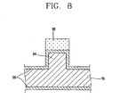
- Figure 8 is a diagram showing a sectional view taken along line VIII-VIII of Figure 7 ;
- Figure 9 is a diagram showing an exploded perspective view of a main body of a mobile terminal in accordance with another preferred embodiment of the present invention.
- Figure 10 is a diagram showing a partially cut perspective view of a main body of the mobile terminal in accordance with another embodiment of the present invention.
- Figure 11 is a diagram showing a perspective view of a carrier of an internal antenna in accordance with another embodiment of the present invention.
- Figure 5 is a diagram showing an exploded perspective view of a main body of a mobile terminal in accordance with one embodiment of the present invention.
- Figure 6 is a diagram showing a partial sectional view of the main body of the mobile terminal of Figure 5 .
- a terminal body 8 having an internal antenna can include cases 50 and 52 enclosing a prescribed space therebetween, a main PCB 54 mounted inside the cases 50 and 52 and having various circuit components mounted thereon and an internal antenna 56 mounted on the main PCB 54.
- the internal antenna 56 can transmit and receive radio waves bearing voice and image information or the like to and from the main PCB 54.
- the case 50 is a front case preferably hinged at a folder 10; and the case 52 is a rear case engaged with the front case 50 to have a certain space therebetween.
- the rear case 52 can include a battery mounting part 60 on which a battery can be mounted.
- the internal antenna 56 can include a carrier 70 fixed at one side of the main PCB 54, a radiator 72 attached at one side of the carrier 70 and radiating radio wave transmitted to and received from the main PCB 54 and a feeding terminal 76 preferably fixed at the carrier 70 and having one end portion connected to the radiator 72 and the other end portion being in contact with an antenna terminal part 74 of the main PCB 54.
- the carrier 70 can include a fixing hole 78 formed at one side, in which the feeding terminal 76 is insertedly fixed, a plurality of engaging hooks 80 formed at a marginal portion thereof and for attaching to the main PCB 54, and screw engaging holes 83 formed at a corner portion thereof so as to be screw-engaged or the like with the front case 50 and the rear case 52.
- an electromagnetic wave shielding part 86 can shield the RF element 82 mounted on the main PCB 54 to thereby reduce or prevent external radiation of electromagnetic wave generated from the RF element 82.
- the carrier 70 can be integrally injection-molded and made of a polycarbonate material or the like.
- the engaging hooks 80 preferably protrude from a marginal portion of the carrier 70 and lock into a hook groove (not shown) formed at the main PCB 54, whereby the carrier 70 is fixed to the main PCB 54.
- the present invention is not intended to be so limited as other fixing devices (e.g., rigidly attached) can be used for coupling the same.
- a connection terminal 90 for electrically coupling the feeding terminal 76 and the radiator 72 is preferably mounted at one side of the fixing hole 78 in which the feeding terminal is insertedly fixed.
- a barrier wall 94 can be formed in a circumferential direction to cover the RF element 82 when the carrier 70 is attached on the main PCB 54. Further, an electromagnetic wave shielding film 96 can be coated at an inner side and an outer side of the electromagnetic wave shielding part 86 to shield electromagnetic wave.
- a gasket 98 is preferably installed at an upper surface of the barrier wall 94 of the electromagnetic wave shielding part 86 being in contact with the surface of the main PCB 54 in order to seal the surface of the main PCB 54 and the electromagnetic wave shielding part 86 to shield electromagnetic wave.
- the electromagnetic wave shielding film 96 can be formed such that a copper film is coated at the surface of the electromagnetic wave shielding part 86 by spraying or vacuum deposition and a corrosion preventing film made of nickel or stainless steel can then be coated at the surface of the copper film by spraying or vacuum deposition.
- the present invention is not intended to be so limited as other materials and processes can be used to form the elctro-magnetic wave shielding film 96 so long as performance criteria are satisfied.
- the gasket 98 is a silicon material having conductivity and elasticity.
- the gasket 98 can be elastically tightly attached at a lower surface of the main PCB 54 to perform an electromagnetic wave shielding function and make an electric grounding.
- an electromagnetic wave shielding film 100 which can be formed by sequentially plating copper and nickel, is preferably coated at an inner side of the front case 50 and the rear case 52 in order to additionally reduce or shield electromagnetic wave generated from parts installed on the main PCB 54.
- the internal antenna 56 In the internal antenna 56, after the feeding terminal 76 is electrically coupled (e.g. fixed) at the carrier 70, the internal antenna 56 is mounted or fixed at one surface (e.g., an upper surface) of the main PCB 54.
- the hook protrusion 80 e.g., formed at the marginal portion of the carrier 70
- the radiator 72 attached to the carrier 70 and the main PCB 54 are electrically coupled.
- the electromagnetic wave shielding part 86 formed at the carrier 70 is tightly attached to the RF element 82 to cover it, thereby shielding electromagnetic waves.
- the front case 50 and the rear case 52 are tightly attached to each other.
- the screw can pass through the screw engaging holes 83 formed at the carrier 70 to engage the carrier 70 together with the front case 50 and the rear case 52.
- the feeding terminal 76 is coupled to the antenna terminal part 74 of the main PCB 54 and the radiator 72 is installed at one side of the carrier 70 for radiating radio wave signal bearing voice and image information generated from the main PCB 54.
- the radio wave signal received through the radiator 72 is received by the antenna terminal part 74 of the main PCB 54 after passing through the feeding terminal 76.
- the RF element 82 of the main PCB 54 is covered by the electromagnetic wave shielding part 86 formed at the carrier 70 and tightly attached to the gasket 98, leakage of electromagnetic wave generated when the RF element 82 operate can be reduced or completely cut off.
- double shielding can be made by the electromagnetic wave shielding film 100 formed at the inner sides of the front case 50 and the rear case 52 around the RF element 82 (e.g., where the electromagnetic wave is mostly generated), and leakage of electromagnetic waves is reduced or prevented by the electromagnetic wave shielding film 100 formed at the front case 50 and the rear case 52 at other remaining regions where the electromagnetic wave is slightly generated (e.g., other components coupled to the main PCB 54). Accordingly, reliable and effective electromagnetic wave shielding can be accomplished.
- Figure 9 is a diagram showing an exploded perspective view of a main body of a mobile terminal in accordance with another embodiment of the present invention.
- Figure 10 is a partially cut perspective view of the main body of the mobile terminal in Figure 9
- Figure 11 is a perspective view of a carrier of an internal antenna in accordance with another embodiment of the present invention.
- FIG. 9 another embodiment of an internal antenna and the mobile terminal housing the same is similar to Figure 5 .
- the embodiment of a carrier 104 of an internal antenna 102 has a different structure.
- the carrier 104 of the internal antenna 102 can include a fixing hole 78 formed at one side thereof, in which the feeding terminal 76 can be insertedly fixed, a plurality of engaging hooks 80 or the like preferably formed at a marginal portion thereof and configured to be fixed to the main PCB 54, and a screw engaging hole 83 or the like preferably formed at a corner portion thereof so as to be screw-engaged with the front case 50 and the rear case 52.
- the front PCB 106 can be a section of the main PCB 54 where electromagnetic wave emitting circuits (e.g., RF element 82) are preferably grouped.
- the first shielding part 110 is preferably formed to cover the RF element at one side of the carrier 104 in order to shield electromagnetic waves generated from the RF element 82, and the second shielding part 112 can be integrally formed at the side of the first shielding part to cover the connector 108 (e.g., FPCB connector) of the front PCB 106.
- the second shielding part 112 can protect the connector 108 and perform an electromagnetic wave shielding operation.
- the connector 108 can be a FPCB connector for connection to a flexible PCB that connects a display module or device (e.g., LCD) in the folder 10 to the main PCB 54.
- the first shielding part 110 and the second shielding part 112 are made of a polycarbonate material.
- the carrier 104, the first shielding part 110 and the second shielding part 112 are integrally injection-molded.
- the present invention is not intended to be so limited as other materials and manufacturing methods can be used.
- a front PCB refuge groove 114 can be formed at the main PCB 54.
- the front PCB refuge groove 114 can allow the front PCB connector 108 to be coupled to an LCD module (e.g., of the folder 10) using a flexible PCB (FPCB).
- the connector 108 of the front PCB 106 can be covered by the second shielding part 112.
- An electromagnetic wave shielding film 96 is preferably coated at an entire surface of the inner side and the outer side of the first shielding part 110 and the second shielding part 112 to shield or reduce electromagnetic waves.
- the electromagnetic wave shielding film 96 can be formed such that a copper film is coated at the surface of the first and second shielding parts 110 and 112 by spraying, vacuum deposition or the like and a corrosion preventing film made of nickel or stainless steel is then coated at the surface of the copper film by spraying, vacuum deposition of the like.
- RF element 82 discharging a large quantity of electromagnetic waves, especially among parts installed on the main PCB 54, and ribs 116 and 118 with a certain height to preferably cover the RF element 82 and the connector 108 of the front PCB 106.
- a gasket 120 can be attached at an upper surface of the ribs 116 and 118 so as to be tightly attached on the surface of the main PCB 54.
- the gasket 120 can be a silicon material having conductivity and elasticity.
- the gasket 98 is elastically tightly attached (e.g., at a lower surface) to the main PCB 54, preferably making an electric grounding.
- embodiments of internal antennas, mobile terminals having an internal antenna and methods for assembling and using the same in accordance with the present invention have various advantages. For example, since an internal antenna can be mounted directly on (e.g., over) the main PCB, a space (e.g., separate from the main PCB) for installation of the antenna is not necessary inside the main body of the terminal. Thus, the terminal can be compact and made smaller. Further, since an electromagnetic wave shielding part for shielding the RF element can be formed in the internal antenna to shield at least one RF element from which a large amount of electromagnetic wave is generated, leakage of electromagnetic wave can be reliably reduced or prevented.
- the electromagnetic wave shielding part can include an electromagnetic wave shielding film on inner and outer surfaces.
- a first shielding part shielding an RF element and the second shield part shielding a front PCB can be formed in an internal antenna
- the RF element generating much electromagnetic wave is double-shielded both by the front PCB shielding part connected to the front PCB and by the electromagnetic wave shielding film formed at an inner side of the casing of the main body.
- electromagnetic waves can be reliably and effectively shielded.
- the internal antenna where the electromagnetic wave shielding member is installed can be simultaneously assembled when the main body casing is assembled, assembly productivity can be enhanced to reduce costs and/or processing time.
Abstract
Description
- The present invention relates to a mobile terminal having an internal antenna.
- In general, a mobile terminal is a wireless communication device that a user can carry along and make a call while traveling. Beyond simple voice transmission and reception, recently, mobile terminals have been fortified in multimedia functions to allow a large amount of information to be transmitted and received. In line with the tendency, performance of an antenna plays a critical role in mobile terminals.
- In addition, as mobile phones are made smaller and more compact in size, the antenna of a mobile terminal is installed in the mobile terminal, rather than exposed. Such an internal antenna is applied to various fields such as a bluetooth, a wireless LAN, a GSM, a CDMA, or the like, and a local area wireless communication.
-
Figure 1 shows a related art mobile terminal. As shown inFigure 1 , the mobile terminal includes a first ormain body 8 having various circuit components embedded therein, amenu button 2 and adial button 4 provided at its front surface and a battery 6 mounted at its rear surface. A second body orfolder 10 displaying various information using adisplay 12 or the like can be hinged or the like at themain body 8. -
Figure 2 is a partial sectional view of the related art mobile terminal. As shown inFigure 2 , themain body 8 of the mobile terminal includes acase 20 having a space therein, a main PCB 22 housed inside thecase 20, and aninternal antenna 24 separately mounted inside thecase 20 and electrically connected to themain PCB 22 to transmit and receive radio waves bearing voice and image information or the like to and from themain PCB 22. - As shown in
Figure 3 , theinternal antenna 24 includes acarrier 30 fixed at an inner side of thecase 20, aradiator 32 formed in a certain pattern at a surface of thecarrier 30 and radiating radio wave that themain PCB 22 transmits and receives, and afeeding terminal 34 connected to theradiator 32 bywire 36. Thefeeding terminal 34 is electrically connected to anantenna terminal unit 28 of themain PCB 22. - In the related art mobile terminal having the internal antenna, voice or image information signal generated from the
main PCB 22 is radiated from theradiator 32 attached on thecarrier 30 through thefeeding terminal 34 connected to theantenna terminal unit 28 of themain PCB 22 and thewire 36 connected therebetween. Further, a radio wave signal received through theradiator 32 is transmitted to themain PCB 22 through thewire 36 connected to theradiator 32 and thefeeding terminal 34. - As shown in
Figure 4 , themain body case 20 is injection-molded, and an electromagneticwave shielding film 40 having a certain thickness is formed as copper and nickel are sequentially plated at an inner side thereof, in order to prevent electromagnetic wave generated fromparts 46 attached to themain PCB 22 from being discharged outwardly. - However, as described above, the related art internal antenna-installed mobile terminal has various disadvantages and problems. For example, since the
carrier 30, which has theradiator 32 for transmitting and receiving voice and image signals attached on its surface, is mounted inside themain body case 20 and connected to themain PCB 22 through thewire 36, a space for installing theinternal antenna 24 must be secured inside themain body case 20. This results in an increase in size of themain body case 20, and accordingly, the overall size of the terminal is increased. - In addition, with the
shielding film 40 coated on the inner side of themain body case 20, it is not possible to completely shield the electromagnetic wave generated from theparts 46 installed at themain PCB 22. Thus, electromagnetic wave generated from parts, such as an RF (Radio Frequency) element, which discharges a large amount of electromagnetic wave can be leaked outwardly. - Document
US 6,392,603 B1 concerns the integration of an RF antenna to an RF shielding part of an RF module. A tuning mechanism is provided for tuning the RF antenna according to a Voltage Standing Wave Ratio (VSWR) specification to thereby tolerate bigger tolerances. - Document
US 2003/0103014 A1 concerns an antenna and a shield for a communication device. In one embodiment, an electromagnetic shield, a spacer and an antenna having an antenna feed is provided out of one substantially continuous piece of conductive material. - Document
US 6,342,869 B1 concerns an antenna device comprising an antenna element provided on a surface of a carrier and connected to a shielding can in which one or more analogue RF components are mounted. The shielding can is connected to and functionally integrated with the antenna element. - The above references are incorporated by reference herein where appropriate for appropriate teachings of additional or alternative details, features and/or technical background.
- An object of the invention is to solve at least the above problems and/or disadvantages and to provide at least the advantages described hereinafter.
- An object of the present invention is to provide a mobile terminal having an internal antenna configured to be mounted on a main PCB and methods thereof so that no additional space is needed for installing the internal antenna inside a main body of the terminal.
- Another object of the present invention is to provide a mobile terminal having an internal antenna capable of reducing or preventing leakage of electromagnetic waves by shielding an RF element among parts installed in a main PCB that discharge electromagnetic waves.
- Another object of the present invention is to provide a mobile terminal having an internal antenna configured to be mounted on a main PCB and capable of reducing or preventing leakage of electromagnetic waves by shielding an RF element among parts installed in a main PCB that discharge electromagnetic wave.
- Another object of the present invention is to provide a mobile terminal having a PCB including a first section grouping mounted circuits configured to emit electromagnetic waves.
- Another object of the present invention is to provide a mobile terminal having a PCB including a first section grouping mounted circuits configured to emit electromagnetic waves and a groove in the first section.
- To achieve at least the above objects in a whole or in part and other advantages and in accordance with the purpose of the present invention, as embodied and broadly described herein, there is provided a mobile terminal having the features of claim 1.
- A mobile terminal may include a terminal case, a PCB provided inside the terminal case and having various circuit components mounted thereon and an internal antenna mounted on the PCB and configured to transmit and receive radio waves bearing voice and image information to and from the PCB and shield electromagnetic wave generating parts mounted on the PCB.
- The mobile terminal includes an internal antenna that includes a carrier inside a communication device and configured to shield electromagnetic wave generating parts, a radiator coupled to the carrier and configured to receive and radiate radio waves transmitted to and received from the communication device and a feeding terminal fixed at the carrier and configured to electrically connect the radiator and an antenna terminal part of the communication device.
- There is provided a mobile terminal that includes a terminal case, a main PCB inside the terminal case and configured to have various circuit components mounted thereon and an internal antenna directly mounted on the main PCB and configured to receive and transmit radio waves bearing voice and image information to and from the main PCB.
- There is provided a method for assembling a mobile terminal that includes providing a terminal case, providing a PCB including various circuit components inside the terminal case and shielding an RF wave generating part mounted on the PCB using the internal antenna.
- There is provided a printed circuit board (PCB) for use with a mobile terminal that includes a first part and a second part of the PCB, RF emitting circuits coupled to an upper surface of the first part of the PCB, a groove formed in the first part, and a connector coupled to the upper surface of the first part and extending through the groove.
- Additional advantages, objects, and features of the invention will be set forth in part in the description which follows and in part will become apparent to those having ordinary skill in the art upon examination of the following or may be learned from practice of the invention. The objects and advantages of the invention may be realized and attained as particularly pointed out in the appended claims.
- The invention will be described in detail with reference to the following drawings in which like reference numerals refer to like elements wherein:
-
Figure 1 is a diagram showing a perspective view of a related art mobile terminal having an internal antenna; -
Figure 2 is a diagram showing a sectional view of a main body of the related art mobile terminal; -
Figure 3 is a diagram showing a perspective view of the internal antenna in accordance with the related art mobile terminal ofFigure 2 ; -
Figure 4 is a diagram showing an enlarged view of a portion 'A' ofFigure 2 ; -
Figure 5 is a diagram showing an exploded perspective view of a main body of a mobile terminal in accordance with a preferred embodiment of the present invention; -
Figure 6 is a diagram showing a partial sectional view of a main body of the mobile terminal in accordance with a preferred embodiment of the present invention; -
Figure 7 is a diagram showing a perspective view of a carrier of the internal antenna in accordance with a preferred embodiment of the present invention; -
Figure 8 is a diagram showing a sectional view taken along line VIII-VIII ofFigure 7 ; -
Figure 9 is a diagram showing an exploded perspective view of a main body of a mobile terminal in accordance with another preferred embodiment of the present invention; -
Figure 10 is a diagram showing a partially cut perspective view of a main body of the mobile terminal in accordance with another embodiment of the present invention; and -
Figure 11 is a diagram showing a perspective view of a carrier of an internal antenna in accordance with another embodiment of the present invention. - Reference will now be made in detail to preferred embodiments of the present invention, examples of which are illustrated in the accompanying drawings. There can be several embodiments of an internal antenna, a mobile terminal having an internal antenna and methods thereof in accordance with the present invention, of which preferred ones will now be described. However, the present invention is not intended to be limited by the following descriptions of preferred embodiments.
-
Figure 5 is a diagram showing an exploded perspective view of a main body of a mobile terminal in accordance with one embodiment of the present invention.Figure 6 is a diagram showing a partial sectional view of the main body of the mobile terminal ofFigure 5 . - In accordance with one embodiment of the present invention, a
terminal body 8 having an internal antenna can includecases main PCB 54 mounted inside thecases internal antenna 56 mounted on themain PCB 54. Theinternal antenna 56 can transmit and receive radio waves bearing voice and image information or the like to and from themain PCB 54. - The
case 50 is a front case preferably hinged at afolder 10; and thecase 52 is a rear case engaged with thefront case 50 to have a certain space therebetween. Therear case 52 can include abattery mounting part 60 on which a battery can be mounted. - The
internal antenna 56 can include acarrier 70 fixed at one side of themain PCB 54, aradiator 72 attached at one side of thecarrier 70 and radiating radio wave transmitted to and received from themain PCB 54 and a feedingterminal 76 preferably fixed at thecarrier 70 and having one end portion connected to theradiator 72 and the other end portion being in contact with anantenna terminal part 74 of themain PCB 54. As shown inFigure 7 , thecarrier 70 can include a fixinghole 78 formed at one side, in which the feedingterminal 76 is insertedly fixed, a plurality of engaginghooks 80 formed at a marginal portion thereof and for attaching to themain PCB 54, andscrew engaging holes 83 formed at a corner portion thereof so as to be screw-engaged or the like with thefront case 50 and therear case 52. At one side of thecarrier 70, an electromagneticwave shielding part 86 can shield theRF element 82 mounted on themain PCB 54 to thereby reduce or prevent external radiation of electromagnetic wave generated from theRF element 82. Thecarrier 70 can be integrally injection-molded and made of a polycarbonate material or the like. - The engaging hooks 80 preferably protrude from a marginal portion of the
carrier 70 and lock into a hook groove (not shown) formed at themain PCB 54, whereby thecarrier 70 is fixed to themain PCB 54. However, the present invention is not intended to be so limited as other fixing devices (e.g., rigidly attached) can be used for coupling the same. - A
connection terminal 90 for electrically coupling the feedingterminal 76 and theradiator 72 is preferably mounted at one side of the fixinghole 78 in which the feeding terminal is insertedly fixed. - For the electromagnetic
wave shielding part 86, abarrier wall 94 can be formed in a circumferential direction to cover theRF element 82 when thecarrier 70 is attached on themain PCB 54. Further, an electromagneticwave shielding film 96 can be coated at an inner side and an outer side of the electromagneticwave shielding part 86 to shield electromagnetic wave. Agasket 98 is preferably installed at an upper surface of thebarrier wall 94 of the electromagneticwave shielding part 86 being in contact with the surface of themain PCB 54 in order to seal the surface of themain PCB 54 and the electromagneticwave shielding part 86 to shield electromagnetic wave. - The electromagnetic
wave shielding film 96 can be formed such that a copper film is coated at the surface of the electromagneticwave shielding part 86 by spraying or vacuum deposition and a corrosion preventing film made of nickel or stainless steel can then be coated at the surface of the copper film by spraying or vacuum deposition. However, the present invention is not intended to be so limited as other materials and processes can be used to form the elctro-magneticwave shielding film 96 so long as performance criteria are satisfied. - As shown in
Figure 8 , thegasket 98 is a silicon material having conductivity and elasticity. Thegasket 98 can be elastically tightly attached at a lower surface of themain PCB 54 to perform an electromagnetic wave shielding function and make an electric grounding. - Like the electromagnetic
wave shielding part 86 formed at thecarrier 70, an electromagneticwave shielding film 100, which can be formed by sequentially plating copper and nickel, is preferably coated at an inner side of thefront case 50 and therear case 52 in order to additionally reduce or shield electromagnetic wave generated from parts installed on themain PCB 54. - An embodiment of an assembly process of the internal antenna in accordance with the present invention will now be described. The embodiment of the assembly processs can be applied to and will be described using the mobile terminal shown in
Figures 5-7 . However, the present invention is not intended to be so limited - In the
internal antenna 56, after the feedingterminal 76 is electrically coupled (e.g. fixed) at thecarrier 70, theinternal antenna 56 is mounted or fixed at one surface (e.g., an upper surface) of themain PCB 54. For example, the hook protrusion 80 (e.g., formed at the marginal portion of the carrier 70) is connected (e.g. locked) into the hook groove (not shown) of themain PCB 54. At this time, as an end portion of the feedingterminal 76 comes in contact with theantenna terminal part 74 of themain PCB 54, theradiator 72 attached to thecarrier 70 and themain PCB 54 are electrically coupled. Further, the electromagneticwave shielding part 86 formed at thecarrier 70 is tightly attached to theRF element 82 to cover it, thereby shielding electromagnetic waves. - Then, the
front case 50 and therear case 52 are tightly attached to each other. For example, when the screw is engaged, the screw can pass through thescrew engaging holes 83 formed at thecarrier 70 to engage thecarrier 70 together with thefront case 50 and therear case 52. - In a mobile terminal having the
internal antenna 56 assembled as described above, the feedingterminal 76 is coupled to theantenna terminal part 74 of themain PCB 54 and theradiator 72 is installed at one side of thecarrier 70 for radiating radio wave signal bearing voice and image information generated from themain PCB 54. The radio wave signal received through theradiator 72 is received by theantenna terminal part 74 of themain PCB 54 after passing through the feedingterminal 76. - Since the
RF element 82 of themain PCB 54 is covered by the electromagneticwave shielding part 86 formed at thecarrier 70 and tightly attached to thegasket 98, leakage of electromagnetic wave generated when theRF element 82 operate can be reduced or completely cut off. In other words, double shielding can be made by the electromagneticwave shielding film 100 formed at the inner sides of thefront case 50 and therear case 52 around the RF element 82 (e.g., where the electromagnetic wave is mostly generated), and leakage of electromagnetic waves is reduced or prevented by the electromagneticwave shielding film 100 formed at thefront case 50 and therear case 52 at other remaining regions where the electromagnetic wave is slightly generated (e.g., other components coupled to the main PCB 54). Accordingly, reliable and effective electromagnetic wave shielding can be accomplished. -
Figure 9 is a diagram showing an exploded perspective view of a main body of a mobile terminal in accordance with another embodiment of the present invention.Figure 10 is a partially cut perspective view of the main body of the mobile terminal inFigure 9 , andFigure 11 is a perspective view of a carrier of an internal antenna in accordance with another embodiment of the present invention. - As shown in
Figure 9 , another embodiment of an internal antenna and the mobile terminal housing the same is similar toFigure 5 . However, the embodiment of acarrier 104 of aninternal antenna 102 has a different structure. - As shown in
Figure 9 , thecarrier 104 of theinternal antenna 102 can include a fixinghole 78 formed at one side thereof, in which the feedingterminal 76 can be insertedly fixed, a plurality of engaginghooks 80 or the like preferably formed at a marginal portion thereof and configured to be fixed to themain PCB 54, and ascrew engaging hole 83 or the like preferably formed at a corner portion thereof so as to be screw-engaged with thefront case 50 and therear case 52. At one side of thecarrier 104, there can be provided afirst shielding part 110 for shielding theRF element 82 mounted on themain PCB 54 and asecond shielding part 112 for shielding aconnector 108 of afront PCB 106. Thefront PCB 106 can be a section of themain PCB 54 where electromagnetic wave emitting circuits (e.g., RF element 82) are preferably grouped. - The
first shielding part 110 is preferably formed to cover the RF element at one side of thecarrier 104 in order to shield electromagnetic waves generated from theRF element 82, and thesecond shielding part 112 can be integrally formed at the side of the first shielding part to cover the connector 108 (e.g., FPCB connector) of thefront PCB 106. Thus, thesecond shielding part 112 can protect theconnector 108 and perform an electromagnetic wave shielding operation. Theconnector 108 can be a FPCB connector for connection to a flexible PCB that connects a display module or device (e.g., LCD) in thefolder 10 to themain PCB 54. - The
first shielding part 110 and thesecond shielding part 112 are made of a polycarbonate material. Thecarrier 104, thefirst shielding part 110 and thesecond shielding part 112 are integrally injection-molded. However, the present invention is not intended to be so limited as other materials and manufacturing methods can be used. - A front
PCB refuge groove 114 can be formed at themain PCB 54. The frontPCB refuge groove 114 can allow thefront PCB connector 108 to be coupled to an LCD module (e.g., of the folder 10) using a flexible PCB (FPCB). Theconnector 108 of thefront PCB 106 can be covered by thesecond shielding part 112. - An electromagnetic
wave shielding film 96 is preferably coated at an entire surface of the inner side and the outer side of thefirst shielding part 110 and thesecond shielding part 112 to shield or reduce electromagnetic waves. The electromagneticwave shielding film 96 can be formed such that a copper film is coated at the surface of the first andsecond shielding parts - At a marginal portion of the first and
second shielding parts RF element 82 discharging a large quantity of electromagnetic waves, especially among parts installed on themain PCB 54, andribs RF element 82 and theconnector 108 of thefront PCB 106. Agasket 120 can be attached at an upper surface of theribs main PCB 54. - The
gasket 120 can be a silicon material having conductivity and elasticity. Thegasket 98 is elastically tightly attached (e.g., at a lower surface) to themain PCB 54, preferably making an electric grounding. - As described above, embodiments of internal antennas, mobile terminals having an internal antenna and methods for assembling and using the same in accordance with the present invention have various advantages. For example, since an internal antenna can be mounted directly on (e.g., over) the main PCB, a space (e.g., separate from the main PCB) for installation of the antenna is not necessary inside the main body of the terminal. Thus, the terminal can be compact and made smaller. Further, since an electromagnetic wave shielding part for shielding the RF element can be formed in the internal antenna to shield at least one RF element from which a large amount of electromagnetic wave is generated, leakage of electromagnetic wave can be reliably reduced or prevented. The electromagnetic wave shielding part can include an electromagnetic wave shielding film on inner and outer surfaces.
- In addition, since a first shielding part shielding an RF element and the second shield part shielding a front PCB (e.g., a connector) can be formed in an internal antenna, the RF element generating much electromagnetic wave is double-shielded both by the front PCB shielding part connected to the front PCB and by the electromagnetic wave shielding film formed at an inner side of the casing of the main body. Thus, electromagnetic waves can be reliably and effectively shielded. Also, since the internal antenna where the electromagnetic wave shielding member is installed can be simultaneously assembled when the main body casing is assembled, assembly productivity can be enhanced to reduce costs and/or processing time.
- The foregoing embodiments and advantages are merely exemplary and are not to be construed as limiting the present invention. The present teaching can be readily applied to other types of apparatuses. The description of the present invention is intended to be illustrative, and not to limit the scope of the claims. Many alternatives, modifications, and variations will be apparent to those skilled in the art. In the claims, means-plus-function clauses are intended to cover the structures described herein as performing the recited function and not only structural equivalents but also equivalent structures.
Claims (16)
- A mobile terminal, comprising:a terminal case (50, 52);a PCB (54) provided inside the terminal case and having various circuit components mounted thereon; andan internal antenna (56) mounted on the PCB (54) and configured to transmit and receive radio waves bearing information to and from the PCB (54) and shield electromagnetic wave generating parts (82) mounted on the PCB (54),wherein the internal antenna (56) comprises:a carrier (70) fixed at one side of the main PCB (54) and configured to have an electromagnetic wave shielding part (86);a radiator (72) attached to the carrier (70) and configured to radiate said radio waves received from the PCB (54); anda feeding terminal (76) coupled to the carrier (70) and configured to electrically connect the radiator (72) and the PCB (54), characterized in that the carrier (70) comprises:a first shielding part (110) configured to shield an RF element(82) mounted on the PCB (54), anda second shielding part (112) configured to shield a connector(108), wherein:the first shielding part (110) is configured to cover the RF element (82) and the second shielding part (112) is configured to cover the connector (108), andthe connector (108) is used for a flexible PCB connection to a folder of the mobile terminal.
- The terminal of claim 1,
wherein the carrier (70) comprises a fixing hole (78) into which the feeding terminal (76) is fixed. - The terminal of claim 1,
wherein the carrier (70) comprises an engaging hole (83), wherein the engaging hole (83) is removably engaged with the terminal case (50). - The terminal of claim 1,
wherein the electromagnetic wave shielding part (86) covers an RF element (82) mounted on the PCB (54). - The terminal of claim 4, wherein the electromagnetic wave shielding part (86) comprises:a barrier wall (94) formed in a circumferential direction so that the RF element (82) can be covered when the carrier (70) is attached on a surface of the PCB (54); andan electromagnetic wave shielding film (96) coated at each of an inner side and an outer side of the electromagnetic wave shielding part (86) for shielding electromagnetic waves.
- The terminal of claim 5,
wherein the electromagnetic wave shielding film (96) comprises a copper film at a surface of the electromagnetic wave shielding part (86) and a corrosion preventing film including nickel or stainless steel at a sur face of the copper film. - The terminal of claim 5,
comprising a gasket (98) at an upper surface of the barrier wall (94) of the electromagnetic wave shielding part (86) configured to seal the barrier wall (94) and the surface of the PCB (54). - The terminal of claim 7,
wherein the gasket (98) comprises a silicon material having both conductivity and elasticity. - The terminal of claim 1, wherein the terminal case comprises:a front case (50) and a rear case (52) determining a prescribed space therebetween; andan electromagnetic wave shielding film (100) at an inner side of the front case (50) and the rear case (52).
- The terminal of claim 9,
wherein the electromagnetic wave shielding film (100) is copper and nickel sequentially plated. - The terminal of claim 1,
wherein the internal antenna (56) is over the PCB (54). - The terminal of claim 1,
wherein the first and second shielding parts (110,112) comprise a polycarbonate material, and wherein the carrier (70), the first shielding part (110) and the second shielding (112) part are integrally formed. - The terminal of claim 1,
wherein an electromagnetic wave shielding film (100) is coated at a surface of the outer side and the inner side of each of the first and second shielding parts for shielding (110, 112) electromagnetic waves. - The terminal of claim 13,
wherein the electromagnetic wave shielding film (100) is a film comprising copper at the surface of the first and second shielding parts (110, 112) and a corrosion preventing film comprising nickel or stainless steel at the surface of the copper film. - The terminal of claim 1,
wherein the first and second shielding parts (110, 112) respectively include a rib (116, 118), wherein a gasket (120) is attached at an upper surface of the rib and configured to be attached between the surface of the PCB (54) and the rib for shielding electromagnetic waves. - The terminal of claim 1,
wherein the PCB (54) comprises a refuge groove (114) so that the connector (108) connected to a front PCB (106) can be covered by the second shielding part (112).
Applications Claiming Priority (4)
| Application Number | Priority Date | Filing Date | Title |
|---|---|---|---|
| KR1020030050711A KR100565279B1 (en) | 2003-07-23 | 2003-07-23 | Inside antenna and mobile phone having thereof |
| KR2003050710 | 2003-07-23 | ||
| KR2003050711 | 2003-07-23 | ||
| KR1020030050710A KR100565278B1 (en) | 2003-07-23 | 2003-07-23 | Mobile terminal having inside type antenna |
Publications (3)
| Publication Number | Publication Date |
|---|---|
| EP1501202A2 EP1501202A2 (en) | 2005-01-26 |
| EP1501202A3 EP1501202A3 (en) | 2005-12-14 |
| EP1501202B1 true EP1501202B1 (en) | 2012-03-28 |
Family
ID=33492560
Family Applications (1)
| Application Number | Title | Priority Date | Filing Date |
|---|---|---|---|
| EP04016987A Not-in-force EP1501202B1 (en) | 2003-07-23 | 2004-07-19 | Internal antenna and mobile terminal having the internal antenna |
Country Status (5)
| Country | Link |
|---|---|
| US (1) | US7541986B2 (en) |
| EP (1) | EP1501202B1 (en) |
| JP (1) | JP4102787B2 (en) |
| CN (1) | CN100397797C (en) |
| AT (1) | ATE551780T1 (en) |
Cited By (1)
| Publication number | Priority date | Publication date | Assignee | Title |
|---|---|---|---|---|
| US9099773B2 (en) | 2006-07-18 | 2015-08-04 | Fractus, S.A. | Multiple-body-configuration multimedia and smartphone multifunction wireless devices |
Families Citing this family (33)
| Publication number | Priority date | Publication date | Assignee | Title |
|---|---|---|---|---|
| US7553295B2 (en) | 2002-06-17 | 2009-06-30 | Iradimed Corporation | Liquid infusion apparatus |
| KR20070038180A (en) * | 2004-08-20 | 2007-04-09 | 코닌클리즈케 필립스 일렉트로닉스 엔.브이. | Wireless terminal, wireless module and method of manufacturing such a terminal |
| US7554494B2 (en) * | 2004-10-21 | 2009-06-30 | Samsung Electronics Co., Ltd. | Built-in antenna module in portable wireless terminal |
| US20060181462A1 (en) * | 2005-02-14 | 2006-08-17 | Intermec Ip Corp. | Integrated antenna/access door for a mobile computer |
| US7627344B2 (en) * | 2006-06-07 | 2009-12-01 | Cingular Wireless Ii, Llc | Universal radio module |
| KR101119113B1 (en) * | 2006-09-29 | 2012-03-16 | 엘지전자 주식회사 | A Mobile Phone |
| US8105282B2 (en) * | 2007-07-13 | 2012-01-31 | Iradimed Corporation | System and method for communication with an infusion device |
| US8472203B2 (en) * | 2007-09-04 | 2013-06-25 | Apple Inc. | Assembly of a handheld electronic device |
| CN101453050B (en) * | 2007-12-07 | 2012-06-27 | 英业达股份有限公司 | Electronic device having antenna grounding structure |
| DE102007062051A1 (en) | 2007-12-21 | 2009-06-25 | Siemens Home And Office Communication Devices Gmbh & Co. Kg | Antenna device for radio-based electronic devices |
| CN101340470B (en) * | 2008-08-12 | 2011-04-06 | 苏州佳世达电通有限公司 | Radio communication device |
| US9172134B2 (en) | 2008-11-06 | 2015-10-27 | Antenna79, Inc. | Protective cover for a wireless device |
| US8214003B2 (en) * | 2009-03-13 | 2012-07-03 | Pong Research Corporation | RF radiation redirection away from portable communication device user |
| CN104752812A (en) | 2008-11-06 | 2015-07-01 | 庞研究有限公司 | Antenna Embedded Into Battery, Wireless Device And Intelligent Outer Shell Of Wireless Device |
| US8957813B2 (en) | 2009-03-13 | 2015-02-17 | Pong Research Corporation | External case for redistribution of RF radiation away from wireless communication device user and wireless communication device incorporating RF radiation redistribution elements |
| KR101127101B1 (en) * | 2009-02-10 | 2012-03-23 | 제일모직주식회사 | In-mold type roof antena and it's manufacturing method |
| KR101025794B1 (en) | 2009-07-14 | 2011-04-04 | (주)블루버드 소프트 | Mobile Terminal |
| KR101164098B1 (en) | 2009-07-14 | 2012-07-12 | (주)블루버드 소프트 | Mobile terminal |
| US9838060B2 (en) | 2011-11-02 | 2017-12-05 | Antenna79, Inc. | Protective cover for a wireless device |
| TWI487478B (en) * | 2012-07-13 | 2015-06-01 | Apone Technology Ltd | Method for forming metal member on casing |
| JP5788069B1 (en) * | 2014-08-29 | 2015-09-30 | 古河電気工業株式会社 | Flat type heat pipe |
| KR20160092875A (en) * | 2015-01-28 | 2016-08-05 | 삼성전기주식회사 | Radiator frame having antenna pattern embeded therein and electronic device including thereof |
| KR102594574B1 (en) * | 2016-01-12 | 2023-10-26 | 삼성전자주식회사 | Radio frequency cable connecting device and electronic device having the same |
| CN107124733A (en) * | 2016-02-24 | 2017-09-01 | 中兴通讯股份有限公司 | Feeder line panel and feeder line connection method |
| KR102527317B1 (en) | 2016-08-30 | 2023-05-03 | 삼성전자주식회사 | Electronic apparatus having metal case with metal pad attached therein |
| WO2018101112A1 (en) * | 2016-11-30 | 2018-06-07 | 株式会社村田製作所 | Wiring board, coupler module, and communication device |
| CN106856524A (en) * | 2016-12-03 | 2017-06-16 | 胡佳培 | A kind of rotating mobile |
| KR102209123B1 (en) | 2017-12-19 | 2021-01-28 | 삼성전자 주식회사 | A module including an antenna and a radio frequency device and base station including the module |
| US11268506B2 (en) | 2017-12-22 | 2022-03-08 | Iradimed Corporation | Fluid pumps for use in MRI environment |
| JP7171455B2 (en) * | 2019-01-21 | 2022-11-15 | Dynabook株式会社 | Electronics |
| US11146301B2 (en) * | 2019-05-09 | 2021-10-12 | William James Scott | Systems and methods for a cellular phone enclosure |
| FR3098810B1 (en) * | 2019-07-18 | 2021-10-15 | Commissariat Energie Atomique | Mechanical connection for MEMS and NEMS device for measuring a pressure variation and device comprising such a mechanical connection |
| WO2024009500A1 (en) * | 2022-07-08 | 2024-01-11 | 日立Astemo株式会社 | Electronic control device and method for manufacturing electronic control device |
Family Cites Families (27)
| Publication number | Priority date | Publication date | Assignee | Title |
|---|---|---|---|---|
| JP2514979B2 (en) | 1987-08-28 | 1996-07-10 | 株式会社東芝 | Electronic device shield structure |
| FI85794C (en) * | 1989-07-05 | 1992-05-25 | Nokia Mobira Oy | FOERFARANDE FOER ATT SKYDDA ETT KRETSKORT ELLER EN DEL DAERAV MOT STOERNINGAR SOM ALSTRATS AV ELEKTROMAGNETISK INTERFERENS, OCH SKYDDSHOELJE FOER ANVAENDNING I FOERFARANDET. |
| US5436802A (en) * | 1994-03-16 | 1995-07-25 | Motorola | Method and apparatus for shielding an electrical circuit that is disposed on a substrate |
| JPH0870195A (en) | 1994-08-29 | 1996-03-12 | Japan Radio Co Ltd | Shielding of printed circuit board |
| SG70987A1 (en) * | 1995-05-09 | 2000-03-21 | Motorola Inc | Method and apparatus for routing conductors |
| JP2898603B2 (en) | 1996-07-02 | 1999-06-02 | 三菱電機株式会社 | Circuit board shield mechanism |
| JPH10150285A (en) | 1996-11-20 | 1998-06-02 | Mitsubishi Electric Corp | Shielding device of electronic circuit |
| US6353443B1 (en) | 1998-07-09 | 2002-03-05 | Telefonaktiebolaget Lm Ericsson (Publ) | Miniature printed spiral antenna for mobile terminals |
| SE9904256D0 (en) * | 1999-02-10 | 1999-11-24 | Allgon Ab | An antenna device and a radio communication device including an antenna device |
| US6200142B1 (en) * | 1999-02-22 | 2001-03-13 | Berg Technology, Inc. | Assembly including a flex circuit and a gas tight chamber |
| US6157546A (en) * | 1999-03-26 | 2000-12-05 | Ericsson Inc. | Shielding apparatus for electronic devices |
| JP2000286584A (en) | 1999-03-30 | 2000-10-13 | Kokusai Electric Co Ltd | Shielding structure of portable-type communication machine |
| US6285324B1 (en) * | 1999-09-15 | 2001-09-04 | Lucent Technologies Inc. | Antenna package for a wireless communications device |
| CN1409942A (en) * | 1999-10-12 | 2003-04-09 | 电子设备屏蔽公司 | EMI shielding apparatus |
| JP2001111321A (en) | 1999-10-13 | 2001-04-20 | Sony Corp | Antenna device and communication terminal equipment |
| SE522419C2 (en) | 1999-10-29 | 2004-02-10 | Ericsson Telefon Ab L M | Module aerial |
| CN1183805C (en) | 1999-12-10 | 2005-01-05 | 热离子体系国际公司 | Thermoplastic laminate fabric heater and methods for making same |
| EP1296544B1 (en) * | 2000-06-30 | 2011-08-03 | Sanyo Electric Co., Ltd. | Flexible printed circuit board and foldable cell phone terminal |
| JP3959945B2 (en) | 2000-10-02 | 2007-08-15 | 松下電器産業株式会社 | High frequency module with antenna |
| JP2002281135A (en) * | 2001-03-21 | 2002-09-27 | Nec Viewtechnology Ltd | Portable telephone |
| US6486837B2 (en) * | 2001-04-09 | 2002-11-26 | Molex Incorporated | Antenna structures |
| JP4304358B2 (en) | 2001-04-20 | 2009-07-29 | 日本電気株式会社 | Mobile phone equipment |
| US20030103014A1 (en) | 2001-12-04 | 2003-06-05 | Thomas Birnbaum | Antenna and shield |
| US7081854B2 (en) * | 2002-05-02 | 2006-07-25 | Sony Ericsson Mobile Communications Ab | Printed built-in antenna for use in a portable electronic communication apparatus |
| WO2003103361A1 (en) * | 2002-06-03 | 2003-12-11 | Mendolia, Greg, S. | Combined emi shielding and internal antenna for mobile products |
| KR100488012B1 (en) * | 2002-11-11 | 2005-05-06 | 엘지전자 주식회사 | Portable computer system |
| US7236065B2 (en) * | 2004-04-28 | 2007-06-26 | Nokia Corporation | Integrated RF-front end having an adjustable antenna |
-
2004
- 2004-07-19 AT AT04016987T patent/ATE551780T1/en active
- 2004-07-19 EP EP04016987A patent/EP1501202B1/en not_active Not-in-force
- 2004-07-22 JP JP2004214990A patent/JP4102787B2/en not_active Expired - Fee Related
- 2004-07-22 US US10/896,059 patent/US7541986B2/en not_active Expired - Fee Related
- 2004-07-23 CN CNB2004100545762A patent/CN100397797C/en not_active Expired - Fee Related
Cited By (1)
| Publication number | Priority date | Publication date | Assignee | Title |
|---|---|---|---|---|
| US9099773B2 (en) | 2006-07-18 | 2015-08-04 | Fractus, S.A. | Multiple-body-configuration multimedia and smartphone multifunction wireless devices |
Also Published As
| Publication number | Publication date |
|---|---|
| EP1501202A3 (en) | 2005-12-14 |
| JP4102787B2 (en) | 2008-06-18 |
| US7541986B2 (en) | 2009-06-02 |
| CN1578173A (en) | 2005-02-09 |
| CN100397797C (en) | 2008-06-25 |
| US20050017910A1 (en) | 2005-01-27 |
| JP2005045810A (en) | 2005-02-17 |
| EP1501202A2 (en) | 2005-01-26 |
| ATE551780T1 (en) | 2012-04-15 |
Similar Documents
| Publication | Publication Date | Title |
|---|---|---|
| EP1501202B1 (en) | Internal antenna and mobile terminal having the internal antenna | |
| US6285327B1 (en) | Parasitic element for a substrate antenna | |
| US7668575B2 (en) | System and method for obtaining radiation characteristics of built-in antenna in mobile communication terminal | |
| US8174452B2 (en) | Cavity antenna for wireless electronic devices | |
| US6563042B2 (en) | Radiating enclosure | |
| US6215454B1 (en) | Multi-layered shielded substrate antenna | |
| US6097339A (en) | Substrate antenna | |
| JP3798733B2 (en) | Wireless module and wireless communication terminal provided with the wireless module | |
| EP1633015B1 (en) | Sealing member and sealing structure of electronic circuit unit | |
| JP2002064601A (en) | Mobile telephone device and its built-in antenna | |
| KR101037898B1 (en) | Emc-arrangement for a device employing wireless data transfer | |
| EP1093675B1 (en) | Substrate antenna incorporating an element preventing the coupling of energy between antenna and conductors | |
| CN110622493B (en) | Communication device and method for assembling a communication device | |
| KR100738265B1 (en) | Substrate antenna | |
| KR100565279B1 (en) | Inside antenna and mobile phone having thereof | |
| JP4814804B2 (en) | Mobile radio communication device | |
| CN108539389B (en) | Middle frame, mobile terminal and manufacturing method of middle frame | |
| JPH11312998A (en) | Portable radio equipment | |
| KR100565278B1 (en) | Mobile terminal having inside type antenna | |
| KR101240844B1 (en) | Set top box having internal antenna | |
| JP2005020766A (en) | Mobile radio equipment | |
| CN112886212B (en) | Wearable electronic equipment | |
| KR200253156Y1 (en) | Antenna of mobile phone | |
| JP2002141724A (en) | Mount structure for antenna |
Legal Events
| Date | Code | Title | Description |
|---|---|---|---|
| PUAI | Public reference made under article 153(3) epc to a published international application that has entered the european phase |
Free format text: ORIGINAL CODE: 0009012 |
|
| 17P | Request for examination filed |
Effective date: 20040719 |
|
| AK | Designated contracting states |
Kind code of ref document: A2 Designated state(s): AT BE BG CH CY CZ DE DK EE ES FI FR GB GR HU IE IT LI LU MC NL PL PT RO SE SI SK TR |
|
| AX | Request for extension of the european patent |
Extension state: AL HR LT LV MK |
|
| RIC1 | Information provided on ipc code assigned before grant |
Ipc: 7H 04M 1/02 B Ipc: 7H 01Q 1/52 B Ipc: 7H 04B 1/38 A |
|
| PUAL | Search report despatched |
Free format text: ORIGINAL CODE: 0009013 |
|
| AK | Designated contracting states |
Kind code of ref document: A3 Designated state(s): AT BE BG CH CY CZ DE DK EE ES FI FR GB GR HU IE IT LI LU MC NL PL PT RO SE SI SK TR |
|
| AX | Request for extension of the european patent |
Extension state: AL HR LT LV MK |
|
| AKX | Designation fees paid |
Designated state(s): AT BE BG CH CY CZ DE DK EE ES FI FR GB GR HU IE IT LI LU MC NL PL PT RO SE SI SK TR |
|
| 17Q | First examination report despatched |
Effective date: 20070703 |
|
| RAP1 | Party data changed (applicant data changed or rights of an application transferred) |
Owner name: LG ELECTRONICS, INC. |
|
| RAP1 | Party data changed (applicant data changed or rights of an application transferred) |
Owner name: LG ELECTRONICS, INC. |
|
| GRAP | Despatch of communication of intention to grant a patent |
Free format text: ORIGINAL CODE: EPIDOSNIGR1 |
|
| GRAS | Grant fee paid |
Free format text: ORIGINAL CODE: EPIDOSNIGR3 |
|
| GRAA | (expected) grant |
Free format text: ORIGINAL CODE: 0009210 |
|
| AK | Designated contracting states |
Kind code of ref document: B1 Designated state(s): AT BE BG CH CY CZ DE DK EE ES FI FR GB GR HU IE IT LI LU MC NL PL PT RO SE SI SK TR |
|
| REG | Reference to a national code |
Ref country code: GB Ref legal event code: FG4D |
|
| REG | Reference to a national code |
Ref country code: CH Ref legal event code: EP |
|
| REG | Reference to a national code |
Ref country code: AT Ref legal event code: REF Ref document number: 551780 Country of ref document: AT Kind code of ref document: T Effective date: 20120415 |
|
| REG | Reference to a national code |
Ref country code: IE Ref legal event code: FG4D |
|
| REG | Reference to a national code |
Ref country code: DE Ref legal event code: R096 Ref document number: 602004037077 Country of ref document: DE Effective date: 20120524 |
|
| REG | Reference to a national code |
Ref country code: NL Ref legal event code: VDEP Effective date: 20120328 |
|
| PG25 | Lapsed in a contracting state [announced via postgrant information from national office to epo] |
Ref country code: FI Free format text: LAPSE BECAUSE OF FAILURE TO SUBMIT A TRANSLATION OF THE DESCRIPTION OR TO PAY THE FEE WITHIN THE PRESCRIBED TIME-LIMIT Effective date: 20120328 Ref country code: GR Free format text: LAPSE BECAUSE OF FAILURE TO SUBMIT A TRANSLATION OF THE DESCRIPTION OR TO PAY THE FEE WITHIN THE PRESCRIBED TIME-LIMIT Effective date: 20120629 |
|
| REG | Reference to a national code |
Ref country code: AT Ref legal event code: MK05 Ref document number: 551780 Country of ref document: AT Kind code of ref document: T Effective date: 20120328 |
|
| PG25 | Lapsed in a contracting state [announced via postgrant information from national office to epo] |
Ref country code: CY Free format text: LAPSE BECAUSE OF FAILURE TO SUBMIT A TRANSLATION OF THE DESCRIPTION OR TO PAY THE FEE WITHIN THE PRESCRIBED TIME-LIMIT Effective date: 20120328 |
|
| PG25 | Lapsed in a contracting state [announced via postgrant information from national office to epo] |
Ref country code: EE Free format text: LAPSE BECAUSE OF FAILURE TO SUBMIT A TRANSLATION OF THE DESCRIPTION OR TO PAY THE FEE WITHIN THE PRESCRIBED TIME-LIMIT Effective date: 20120328 Ref country code: SE Free format text: LAPSE BECAUSE OF FAILURE TO SUBMIT A TRANSLATION OF THE DESCRIPTION OR TO PAY THE FEE WITHIN THE PRESCRIBED TIME-LIMIT Effective date: 20120328 Ref country code: CZ Free format text: LAPSE BECAUSE OF FAILURE TO SUBMIT A TRANSLATION OF THE DESCRIPTION OR TO PAY THE FEE WITHIN THE PRESCRIBED TIME-LIMIT Effective date: 20120328 Ref country code: SI Free format text: LAPSE BECAUSE OF FAILURE TO SUBMIT A TRANSLATION OF THE DESCRIPTION OR TO PAY THE FEE WITHIN THE PRESCRIBED TIME-LIMIT Effective date: 20120328 Ref country code: RO Free format text: LAPSE BECAUSE OF FAILURE TO SUBMIT A TRANSLATION OF THE DESCRIPTION OR TO PAY THE FEE WITHIN THE PRESCRIBED TIME-LIMIT Effective date: 20120328 Ref country code: PL Free format text: LAPSE BECAUSE OF FAILURE TO SUBMIT A TRANSLATION OF THE DESCRIPTION OR TO PAY THE FEE WITHIN THE PRESCRIBED TIME-LIMIT Effective date: 20120328 Ref country code: BE Free format text: LAPSE BECAUSE OF FAILURE TO SUBMIT A TRANSLATION OF THE DESCRIPTION OR TO PAY THE FEE WITHIN THE PRESCRIBED TIME-LIMIT Effective date: 20120328 |
|
| PG25 | Lapsed in a contracting state [announced via postgrant information from national office to epo] |
Ref country code: PT Free format text: LAPSE BECAUSE OF FAILURE TO SUBMIT A TRANSLATION OF THE DESCRIPTION OR TO PAY THE FEE WITHIN THE PRESCRIBED TIME-LIMIT Effective date: 20120730 Ref country code: SK Free format text: LAPSE BECAUSE OF FAILURE TO SUBMIT A TRANSLATION OF THE DESCRIPTION OR TO PAY THE FEE WITHIN THE PRESCRIBED TIME-LIMIT Effective date: 20120328 |
|
| PG25 | Lapsed in a contracting state [announced via postgrant information from national office to epo] |
Ref country code: DK Free format text: LAPSE BECAUSE OF FAILURE TO SUBMIT A TRANSLATION OF THE DESCRIPTION OR TO PAY THE FEE WITHIN THE PRESCRIBED TIME-LIMIT Effective date: 20120328 Ref country code: NL Free format text: LAPSE BECAUSE OF FAILURE TO SUBMIT A TRANSLATION OF THE DESCRIPTION OR TO PAY THE FEE WITHIN THE PRESCRIBED TIME-LIMIT Effective date: 20120328 Ref country code: AT Free format text: LAPSE BECAUSE OF FAILURE TO SUBMIT A TRANSLATION OF THE DESCRIPTION OR TO PAY THE FEE WITHIN THE PRESCRIBED TIME-LIMIT Effective date: 20120328 |
|
| PLBE | No opposition filed within time limit |
Free format text: ORIGINAL CODE: 0009261 |
|
| STAA | Information on the status of an ep patent application or granted ep patent |
Free format text: STATUS: NO OPPOSITION FILED WITHIN TIME LIMIT |
|
| PG25 | Lapsed in a contracting state [announced via postgrant information from national office to epo] |
Ref country code: MC Free format text: LAPSE BECAUSE OF NON-PAYMENT OF DUE FEES Effective date: 20120731 |
|
| REG | Reference to a national code |
Ref country code: CH Ref legal event code: PL |
|
| 26N | No opposition filed |
Effective date: 20130103 |
|
| REG | Reference to a national code |
Ref country code: DE Ref legal event code: R097 Ref document number: 602004037077 Country of ref document: DE Effective date: 20130103 |
|
| PG25 | Lapsed in a contracting state [announced via postgrant information from national office to epo] |
Ref country code: LI Free format text: LAPSE BECAUSE OF NON-PAYMENT OF DUE FEES Effective date: 20120731 Ref country code: CH Free format text: LAPSE BECAUSE OF NON-PAYMENT OF DUE FEES Effective date: 20120731 |
|
| REG | Reference to a national code |
Ref country code: IE Ref legal event code: MM4A |
|
| PG25 | Lapsed in a contracting state [announced via postgrant information from national office to epo] |
Ref country code: BG Free format text: LAPSE BECAUSE OF FAILURE TO SUBMIT A TRANSLATION OF THE DESCRIPTION OR TO PAY THE FEE WITHIN THE PRESCRIBED TIME-LIMIT Effective date: 20120628 Ref country code: IE Free format text: LAPSE BECAUSE OF NON-PAYMENT OF DUE FEES Effective date: 20120719 |
|
| PG25 | Lapsed in a contracting state [announced via postgrant information from national office to epo] |
Ref country code: ES Free format text: LAPSE BECAUSE OF FAILURE TO SUBMIT A TRANSLATION OF THE DESCRIPTION OR TO PAY THE FEE WITHIN THE PRESCRIBED TIME-LIMIT Effective date: 20120709 |
|
| PG25 | Lapsed in a contracting state [announced via postgrant information from national office to epo] |
Ref country code: TR Free format text: LAPSE BECAUSE OF FAILURE TO SUBMIT A TRANSLATION OF THE DESCRIPTION OR TO PAY THE FEE WITHIN THE PRESCRIBED TIME-LIMIT Effective date: 20120328 |
|
| PG25 | Lapsed in a contracting state [announced via postgrant information from national office to epo] |
Ref country code: LU Free format text: LAPSE BECAUSE OF NON-PAYMENT OF DUE FEES Effective date: 20120719 |
|
| PG25 | Lapsed in a contracting state [announced via postgrant information from national office to epo] |
Ref country code: HU Free format text: LAPSE BECAUSE OF FAILURE TO SUBMIT A TRANSLATION OF THE DESCRIPTION OR TO PAY THE FEE WITHIN THE PRESCRIBED TIME-LIMIT Effective date: 20040719 |
|
| REG | Reference to a national code |
Ref country code: FR Ref legal event code: PLFP Year of fee payment: 12 |
|
| PGFP | Annual fee paid to national office [announced via postgrant information from national office to epo] |
Ref country code: GB Payment date: 20150615 Year of fee payment: 12 |
|
| PGFP | Annual fee paid to national office [announced via postgrant information from national office to epo] |
Ref country code: FR Payment date: 20150612 Year of fee payment: 12 |
|
| PGFP | Annual fee paid to national office [announced via postgrant information from national office to epo] |
Ref country code: DE Payment date: 20150612 Year of fee payment: 12 |
|
| PGFP | Annual fee paid to national office [announced via postgrant information from national office to epo] |
Ref country code: IT Payment date: 20150710 Year of fee payment: 12 |
|
| REG | Reference to a national code |
Ref country code: DE Ref legal event code: R119 Ref document number: 602004037077 Country of ref document: DE |
|
| GBPC | Gb: european patent ceased through non-payment of renewal fee |
Effective date: 20160719 |
|
| PG25 | Lapsed in a contracting state [announced via postgrant information from national office to epo] |
Ref country code: FR Free format text: LAPSE BECAUSE OF NON-PAYMENT OF DUE FEES Effective date: 20160801 Ref country code: DE Free format text: LAPSE BECAUSE OF NON-PAYMENT OF DUE FEES Effective date: 20170201 |
|
| REG | Reference to a national code |
Ref country code: FR Ref legal event code: ST Effective date: 20170331 |
|
| PG25 | Lapsed in a contracting state [announced via postgrant information from national office to epo] |
Ref country code: GB Free format text: LAPSE BECAUSE OF NON-PAYMENT OF DUE FEES Effective date: 20160719 |
|
| PG25 | Lapsed in a contracting state [announced via postgrant information from national office to epo] |
Ref country code: IT Free format text: LAPSE BECAUSE OF NON-PAYMENT OF DUE FEES Effective date: 20160719 |