EP1517376B1 - Display panel, method of manufacturing display panel, and display apparatus - Google Patents
Display panel, method of manufacturing display panel, and display apparatus Download PDFInfo
- Publication number
- EP1517376B1 EP1517376B1 EP04255583.9A EP04255583A EP1517376B1 EP 1517376 B1 EP1517376 B1 EP 1517376B1 EP 04255583 A EP04255583 A EP 04255583A EP 1517376 B1 EP1517376 B1 EP 1517376B1
- Authority
- EP
- European Patent Office
- Prior art keywords
- layer
- light
- display panel
- conductivity
- control
- Prior art date
- Legal status (The legal status is an assumption and is not a legal conclusion. Google has not performed a legal analysis and makes no representation as to the accuracy of the status listed.)
- Expired - Fee Related
Links
Images


Classifications
-
- H—ELECTRICITY
- H10—SEMICONDUCTOR DEVICES; ELECTRIC SOLID-STATE DEVICES NOT OTHERWISE PROVIDED FOR
- H10K—ORGANIC ELECTRIC SOLID-STATE DEVICES
- H10K50/00—Organic light-emitting devices
- H10K50/80—Constructional details
- H10K50/805—Electrodes
-
- H—ELECTRICITY
- H05—ELECTRIC TECHNIQUES NOT OTHERWISE PROVIDED FOR
- H05B—ELECTRIC HEATING; ELECTRIC LIGHT SOURCES NOT OTHERWISE PROVIDED FOR; CIRCUIT ARRANGEMENTS FOR ELECTRIC LIGHT SOURCES, IN GENERAL
- H05B33/00—Electroluminescent light sources
- H05B33/12—Light sources with substantially two-dimensional radiating surfaces
- H05B33/26—Light sources with substantially two-dimensional radiating surfaces characterised by the composition or arrangement of the conductive material used as an electrode
-
- H—ELECTRICITY
- H04—ELECTRIC COMMUNICATION TECHNIQUE
- H04N—PICTORIAL COMMUNICATION, e.g. TELEVISION
- H04N9/00—Details of colour television systems
- H04N9/12—Picture reproducers
- H04N9/30—Picture reproducers using solid-state colour display devices
-
- H—ELECTRICITY
- H05—ELECTRIC TECHNIQUES NOT OTHERWISE PROVIDED FOR
- H05B—ELECTRIC HEATING; ELECTRIC LIGHT SOURCES NOT OTHERWISE PROVIDED FOR; CIRCUIT ARRANGEMENTS FOR ELECTRIC LIGHT SOURCES, IN GENERAL
- H05B33/00—Electroluminescent light sources
- H05B33/10—Apparatus or processes specially adapted to the manufacture of electroluminescent light sources
-
- H—ELECTRICITY
- H10—SEMICONDUCTOR DEVICES; ELECTRIC SOLID-STATE DEVICES NOT OTHERWISE PROVIDED FOR
- H10K—ORGANIC ELECTRIC SOLID-STATE DEVICES
- H10K59/00—Integrated devices, or assemblies of multiple devices, comprising at least one organic light-emitting element covered by group H10K50/00
- H10K59/80—Constructional details
- H10K59/805—Electrodes
-
- H—ELECTRICITY
- H10—SEMICONDUCTOR DEVICES; ELECTRIC SOLID-STATE DEVICES NOT OTHERWISE PROVIDED FOR
- H10K—ORGANIC ELECTRIC SOLID-STATE DEVICES
- H10K50/00—Organic light-emitting devices
- H10K50/80—Constructional details
-
- H—ELECTRICITY
- H10—SEMICONDUCTOR DEVICES; ELECTRIC SOLID-STATE DEVICES NOT OTHERWISE PROVIDED FOR
- H10K—ORGANIC ELECTRIC SOLID-STATE DEVICES
- H10K59/00—Integrated devices, or assemblies of multiple devices, comprising at least one organic light-emitting element covered by group H10K50/00
- H10K59/10—OLED displays
- H10K59/17—Passive-matrix OLED displays
- H10K59/173—Passive-matrix OLED displays comprising banks or shadow masks
-
- H—ELECTRICITY
- H10—SEMICONDUCTOR DEVICES; ELECTRIC SOLID-STATE DEVICES NOT OTHERWISE PROVIDED FOR
- H10K—ORGANIC ELECTRIC SOLID-STATE DEVICES
- H10K59/00—Integrated devices, or assemblies of multiple devices, comprising at least one organic light-emitting element covered by group H10K50/00
- H10K59/30—Devices specially adapted for multicolour light emission
- H10K59/35—Devices specially adapted for multicolour light emission comprising red-green-blue [RGB] subpixels
Definitions
- the present invention relates to a display panel, a method of manufacturing a display panel, and a display apparatus, and more particularly to the technology of a display panel for use in a display apparatus which is controllable by light.
- an organic electroluminescence (hereinbelow, termed "EL") display has been employed as an image display apparatus.
- EL organic electroluminescence
- As the technology of the organic EL display there has been, for example, one proposed in “ Organic EL materials and Displays", CMC, ISBN: 4-88231-284-0 C3054, Chapter 19, “Driving method for Organic EL display”, Shingo Kawashima, pp. 279-289
- the organic EL display in the prior art is such that thin film transistor (hereinbelow, termed "TFT") elements made from low-temperature poly-silicon, amorphous silicon or the like are disposed in regions which correspond respectively to pixels.
- TFT thin film transistor
- Each TFT element has its ON/OFF state controlled by access which employs current.
- the organic EL display can be driven in such a way that the ON/OFF states of the respective TFT elements are controlled by employing currents.
- the TFT element is provided for every pixel, also the number of TFT elements increases in accordance with the increase of the number of pixels.
- the number of electrical wiring lines for accessing the TFT elements with currents increases.
- the increase of the number of TFT elements results in increasing also the number of electrical wiring lines, it can form a cause for incurring the increase of an electrical resistance.
- the electrical resistance increases, it becomes difficult to make the accesses by causing sufficient currents to pervade all the TFT elements.
- the TFT elements of the screen disperse, a display image becomes nonuniform. In this manner, the uniform manufacture of the TFT elements is difficult in addition to the possible sudden rise of the manufacturing cost, so that the manufacture of the large-sized screen is difficult.
- the prior-art organic EL display is problematic in the case of enlarging the size of the screen, because of the difficulty in the driving aspect in the accesses to the TFT elements, and the difficulty in the manufacturing aspect.
- EP 0382642 discloses a monochromatic display device comprising, on a substrate, an electroluminescent layer and a photoconductive layer which are stacked up. This stack is interposed between two electrode systems serving to excite the electroluminescent layer, the electroluminescent layer having an emission spectrum encompassing the sensitivity spectrum of the photoconductive material.
- An optical filter is arranged between the electroluminescent layer and the observer of the device and lets through that portion of the emission spectrum of the electroluminescent layer most useful to the display. The optical filter blocks a region of the emission spectrum of the ambient lighting, the sensitivity spectrum of the photoconductive layer then essentially being contained in this region.
- US 5200668 discloses an injection type thin film luminescence element having two electrode layers at least one of which is transparent or translucent, and having between these two electrode layers a luminescence function-manifesting layer comprising a laminated layer of a p-type or n-type inorganic semiconductor thin film layer and an organic compound thin film layer.
- US 5539424 discloses a thin-film EL display device of red luminescent color.
- the thin-film EL display device has a first transparent electrode, a first transparent insulating layer, a light-emitting layer of zinc sulfide (ZnS) with the addition of manganese (Mn), a red-light transmitting filter of amorphous silicon (a-Si), a second transparent insulating layer, and a second transparent electrode, which are successively deposited one on top of another on a glass substrate.
- the EL display device produces red light from orange light emission from the light-emitting layer.
- US 2002/167268 discloses a color display substrate, having plural color display elements arranged in a matrix pattern, and a manufacturing method for obtaining a color filter substrate and color luminescent substrate.
- the manufacturing method of a color display substrate includes the step of forming plural color dots by selectively ejecting liquid droplets from nozzles in accordance with input data.
- the plural color dots constitute plural pixels, which constitute plural color filter elements arranged in a matrix pattern.
- the plural color dots have a first dot pitch in a direction perpendicular to a first base line.
- Each of the plural color dots is formed to lie at a distance of at least substantially an integral multiple of the first dot pitch from the first base line.
- the present invention has been made in view of the above problems, and it has for its object to provide a display panel easy of enlarging a size, a method of manufacturing the display panel, and a display apparatus employing the display panel.
- a display panel as defined in claim 1.
- the display panel of the present invention is driven by entering the control light into the first transparent electrode layer.
- the conductivity-variable layer When the control light is not entered, the conductivity-variable layer functions as an insulating layer whose electrical conductivity is substantially zero. Besides, when the control light is entered, the conductivity-variable layer has its electrical conductivity changed in accordance with the light quantity of the control light transmitted through the first transparent electrode layer.
- the conductivity-variable layer controls the voltage applied to the electroluminescent layer when a voltage is applied between the first and second transparent electrode layers, in response to the quantity of control light entering the conductivity-variable layer.
- the voltage corresponding to the light quantity of the control light is applied to the EL layer, whereby this EL layer emits the light in correspondence with the light quantity of the control light. In this way, the display panel can have its drive controlled by accessing it with the control light (light addressing).
- the display panel of the present invention Since the display panel of the present invention is controllable by entering the control light thereinto, it need not be provided with TFT elements. Whereas the TFT elements need to be disposed in respective regions corresponding to pixels, the conductivity-variable layer, first transparent electrode layer and second transparent electrode layer can be formed by forming films uniformly over the whole substrate, so that the display panel of the present invention can be manufactured with ease. Moreover, the respective pixels can be accessed by the construction which allows the control light to scan, so that they need not be electrically accessed. For this reason, electrical wiring lines need not be laid for the respective pixels. Therefore, the display panel of the present invention can be made simpler in construction than a prior-art EL display. Owing to the simplified construction of the display panel, the yield thereof can be increased to curtail a manufacturing cost.
- the display panel of the present invention can be manufactured by chiefly forming the films of materials constituting the respective layers, uniformly over the whole substrate, so that even a large-sized screen is easy of manufacture. Besides, the display panel of the present invention need not electrically access the respective pixels, so that an electrical resistance does not increase even when the number of pixels is increased.
- the electrical resistance is not increased even by the increase of the number of pixels, even a large-sized display panel can have its drive controlled with ease as long as the control light can be entered into the whole display panel. Further, owing to the non-increase of the electrical resistance and also to the low dissipation power of the EL layer itself, dissipation power in the case of enlarging the size of the display panel can be decreased. Thus, the display panel easy of enlarging the size is obtained.
- a display panel should desirably comprise an optical system for control light, which is adapted to supply the control light to said display panel; and a light shield portion which is provided near a surface of said first electrode layer at which the control light from the optical system enters the display panel, and which is formed with openings in correspondence with the pixels; wherein each of the openings is arranged at a position through which the control light from the optical system passes, so that the control light enters the first electrode layer at a position corresponding to a predetermined one of the pixels; and the electroluminescent layer is adapted to emit light at the region corresponding to the predetermined pixel in response to the control light.
- the control light After having passed through the openings provided in the light shield portion, the control light is entered into the first transparent electrode layer.
- Each of the openings is arranged at the position through which the control light is passed to be entered into the part of the first transparent electrode layer corresponding to the predetermined pixel.
- the control light can be entered into only the part of the first transparent electrode layer corresponding to the predetermined pixel.
- control light In a case where the control light has proceeded toward the part of the first transparent electrode layer corresponding to any pixel different from the predetermined pixel, it is intercepted by the light shield portion. In this manner, the light shield portion and the openings corresponding to the pixels are provided, whereby the control light can be prevented from erroneously entering the region which corresponds to the pixel other than the predetermined pixel. Besides, in a case where a plurality of control lights are entered into regions which correspond to pixels different from one another, it is allowed to employ a construction in which the plurality of control lights are passed through one opening.
- control lights are allowed to scan at a precision enough to enter into the opening, whereby the control lights can be precisely entered into only the parts of the first transparent electrode layer corresponding to predetermined pixels even when the entrance positions of the control lights are not controlled at a still higher precision.
- the scanning speed of the control lights need not be made slow, the light addressing can be precisely performed without degrading the quality of an image. Thus, a precise control can be performed with ease.
- the EL layer has a structure in which it is divided into a plurality of regions corresponding to the pixels, preferably by a plurality of partition members provided on the conductivity-variable layer.
- the EL layer is made the structure in which it is divided into the plurality of pixels, by providing the partition members on the conductivity-variable layer.
- the conductivity-variable layer has its conductivity changed only under the partition member.
- the conductivity of the conductivity-variable layer changes only under the partition member, it is sometimes impossible to apply a sufficient voltage to the EL layer, so the EL layer fails to emit light.
- the display panel of the present invention dispenses with TFT elements, electric wiring lines need not be laid under the partition members. Therefore, the regions of the reflection electrode can be spread to spaces underlying the partition members.
- the region of the reflection electrode corresponding to each pixel becomes larger than the part of the EL layer divided into pixels by the partition members, to the amount of a region held between the partition members and the conductivity-variable layer. Since the region of the reflection electrode corresponding to each pixel is larger than the region of the part of the EL layer divided by the partition members, it is possible to utilize the control light which has entered a larger area than in the case where the reflection electrode is divided in correspondence with the pixels similarly to the EL layer. Besides, since the control light having entered the larger area can be utilized, the control of the display panel can be satisfactorily performed even when it is difficult to control the entrance position of the control light at a high precision. Thus, the EL layer can be efficiently caused to emit light.
- the conductivity-variable layer should desirably have a structure in which it is divided into a plurality of regions corresponding to the pixels.
- a region in which the conductivity of the conductivity-variable layer changes, tends to spread to the surroundings around the irradiation position of the control light in proportion to the intensity of the control light and the irradiation time period thereof.
- the plurality of regions of the EL layer are provided in correspondence with pixels for first color light, pixels for second color light, and pixels for third color light; that each pixel aggregate is constructed of one of the pixels for the first color light, one of the pixels for the second color light, and one of the pixels for the third color light; and that a plurality of such pixel aggregates are provided at substantially equal intervals in two predetermined directions being substantially orthogonal to each other.
- a full-color image is displayed by the pixels for the first color light, the pixels for the second color light, and the pixels for the third color light.
- each pixel aggregate is constructed of the pixel for the first color light, the pixel for the second color light, and the pixel for the third color light, the pixels can be densely arrayed.
- the aperture percentage of the display panel is enhanced, and a bright image is obtained.
- the plurality of pixel aggregates are arrayed at the substantially equal intervals in the two-dimensional directions, the distortion of an image can be reduced to precisely display the image. Thus, a bright and precise full-color image is obtained.
- the display panel stated before can be manufactured. Besides, since the display panel stated before dispenses with TFT elements, the layers of parts, which are other than the partition members for defining the pixels and the EL layer provided in correspondence with the pixels, can be formed by forming films over the whole surface of the substrate. Therefore, the display panel can be manufactured with ease.
- a display panel In a case where a display panel is provided with TFT elements, it needs to be manufactured so that the positions of the electrodes of the TFT elements may be registered with the positions of an EL layer corresponding to pixels.
- the display panel stated before dispenses with the TFT elements.
- the EL layer need not have its positions registered as in the case of providing the TFT elements, and it may well be constructed in correspondence with pixels, on the conductivity-variable layer formed over the whole surface of the first substrate. Therefore, the first layered structure which is formable over the whole surface of the first substrate, and the second layered structure which has the structure corresponding to the pixels can be respectively formed as separate members.
- the first layered structure and the second layered structure are stuck to each other into the unitary structure, whereby the display panel can be manufactured.
- the second layered structure can be formed by successively stacking the second transparent electrode layer and the EL layer on the second substrate.
- the protective layer can be made a more rigid member than in a case of forming the protective layer on the layered structure which corresponds to the pixels.
- the protective layer of the display panel can be made rigid, so that the manufactured display panel can be used for a long term.
- a display apparatus as defined in claim 8.
- the display apparatus of the present invention is controlled by entering the control light from the optical system for the control light.
- the voltage for causing the EL layer to emit light is applied between the first transparent electrode layer and the second transparent electrode layer. Since the voltage for causing the EL layer to emit light is applied by the power source, the intensity of the control light may be to the extent of changing the electrical conductivity of the conductivity-variable layer. Therefore, the optical system for the control light can be used for the display apparatus of the present invention even when it is difficult of generating control light of high intensity. Since the control light of high intensity need not be generated, the display apparatus can be used safely. Besides, since the display panel stated before is used, dissipation power is low, and the enlargement of the size of the display panel is easy.
- the optical system for the control light scans the first transparent electrode layer with the control light of beam shape.
- the display apparatus of the present invention does not require a vacuum tube as in, for example, a display apparatus employing a CRT, so that it can be made light in weight even when the display panel is made large in size.
- the control light can have its proceeding direction deflected by a mirror and can be fined by a lens. Therefore, even when the display apparatus is thinned, the control light can scan over the whole large-sized display panel by, for example, bending the proceeding direction of the control light with a mirror. Further, by bending the proceeding direction of the control light, the optical path of the control light becomes long with the display apparatus kept small in size. Therefore, the scanning angle of the control light can be narrowed. Thus, a display apparatus capable of easily enlarging the size of the display panel is obtained.
- the optical system for the control light includes a plurality of light source units for the control lights; that each of the light source units for the control lights consists of a first light source portion to supply first control light to a part of the first transparent electrode layer corresponding to a pixel for first color light, a second light source portion to supply second control light to a part of the first transparent electrode layer corresponding to a pixel for second color light, and a third light source portion to supply third control light to a part of the first transparent electrode layer corresponding to a pixel for third color light; and that the plurality of light source units for the control lights supply the first control light, the second control light and the third control light to different regions of the display panel, respectively.
- the control lights are supplied in such a way that the respective light source units for the control lights take charge of the different regions of the display panel, whereby distances from galvanomirrors to the display panel can be shortened. Moreover, the control lights are supplied by allotting the different regions of the display panel to the light source units, whereby the scanning angles of the control lights can be narrowed. Since the scanning distances of the control lights are shortened, an image display can be satisfactorily performed even when the scanning speeds of the control lights are lowered. Thus, the display apparatus can be made small in size, and besides, the control lights can be easily allowed to scan.
- the frame in which at least the optical system for the control light is accommodated; wherein the display panel is mounted on the frame. Since the display panel stated before is mounted on the frame, the frame can be made light in weight and thin in structure even when the display panel is enlarged in size. Thus, a display apparatus which is easy of enlarging the size of the display panel is obtained.
- the display panel is arranged with the first transparent electrode layer thereof held in opposition to the display of the other image display apparatus, and the light from the display is entered into the first transparent electrode layer of the display panel as the control light.
- the conductivity-variable layer has its conductivity changed in accordance with the light quantity of the light from the display, at its position corresponding to that position of the first transparent electrode layer into which the light from the display has been entered.
- the EL layer is provided uniformly over the whole surface of the display panel, it can be caused to emit light in accordance with the position and light quantity of the light from the display as has been entered into the first transparent electrode layer, thereby to display an image.
- the display panel can be driven by entering the light from the display into the first transparent electrode layer.
- color filters are provided on the entrance side of the display panel for the light from the display and on the exit side of the display panel for the emitted light, whereby a full-color image can be obtained in the display panel.
- a display panel capable of displaying the image of the other image display apparatus is obtained with the simple construction.
- Fig. 1 shows the schematic construction of a display apparatus 100 according to Embodiment 1 of the present invention.
- the display apparatus 100 is constructed of a display panel 120, a power source 130, and an optical system for control light, 140.
- the display panel 120 displays an image by causing an organic EL layer 110 to emit light.
- a substrate 101 is a parallel flat plate which is made of a glass member, a polymer member or the like which is optically transparent.
- a first transparent electrode layer 102 being optically transparent, and a conductivity-variable layer 103 are successively stacked on the substrate 101.
- the first transparent electrode layer 102 can be made of an ITO film.
- the conductivity-variable layer 103 has its electrical conductivity changed by the control light L transmitted through the first transparent electrode layer 102.
- Amorphous silicon (hereinbelow, termed "a-Si”) or a photosensitive organic film, for example, can be employed for the conductivity-variable layer 103.
- the a-Si for example, should desirably contain hydrogen.
- the a-Si is formed by chemical vapor deposition (CVD).
- CVD chemical vapor deposition
- the conductivity enlarges (that is, the resistance value becomes small) in accordance with the quantity of the light. That region of the conductivity-variable layer 103 in which the conductivity changes corresponds to that region of the first transparent electrode layer 102 which has irradiated the a-Si with the control light L.
- the organic EL layer 110 is provided on the conductivity-variable layer 103.
- the organic EL layer 110 is constructed in such a way that a reflection electrode 111, an ITO film 112, a hole transport layer 113, an organic light emission layer 114 and an electron transport layer 115 are successively stacked from the side of the conductivity-variable layer 103.
- the reflection electrode 111 can be constructed by evaporating a metal, for example, aluminum (Al).
- the ITO film 112 is provided in order to promote the emission of charges from the reflection electrode 111 into the hole transport layer 113.
- a triazole derivative for example, can be employed as the material of the hole transport layer 113.
- a benzothiazolic compound for example, can be employed for the organic light emission layer 114.
- An electron-transmissive compound for example, diphenylquinone derivative can be employed for the electron transport layer 115. Since any of the hole transport layer 113, organic light emission layer 114 and electron transport layer 115 has a thickness on the order of several tens nm, it is optically transparent.
- a second transparent electrode layer 104 can be made of an ITO film likewise to the first transparent electrode layer 102.
- a protective layer 105 which is made of an optically transparent member similar to the substrate 101, is provided on the second transparent electrode layer 104.
- the display panel 120 has a voltage applied between the first transparent electrode layer 102 and the second transparent electrode layer 104 by the power source 130.
- the construction of the organic EL layer 110 is not restricted to the above one.
- a bonding layer may well be provided for any of the individual layers constituting the organic EL layer 110.
- a hole transport material and an electron transport material may well be mixed into the organic light emission layer 114 by providing neither of the hole transport layer 113 and the electron transport layer 115. If the charges of the reflection electrode 111 can be sufficiently emitted into the hole transport layer 113, the ITO film 112 may well be omitted.
- the optical system for the control light, 140 is constructed of a galvanomirror 144, and a light source portion for the control light, 142.
- the optical system for the control light, 140 is disposed for the display panel 120 and on the side of the substrate 101.
- the light source portion for the control light, 142 supplies the control light L which is beam-shaped light, for example, laser light.
- a semiconductor laser element or a surface-light-emission laser element which is furnished with a modulator can be employed for the light source portion for the control light, 142.
- the light source portion for the control light, 142 can modulate the intensity of the control light L in accordance with an image signal from a control portion 148, so as to supply the modulated light.
- the control light L from the light source portion for the control light, 142 is reflected toward the display panel 120 by the galvanomirror 144. Besides, the control light L reflected toward the display panel 120 enters that surface of the display panel 120 which lies on the side of the substrate 101.
- the galvanomirror 144 can be fabricated by, for example, MEMS (Micro Electro Mechanical Systems) technology.
- the galvanomirror 144 turns about two predetermined axes being substantially orthogonal to each other, thereby allowing the control light L to scan in two directions.
- the turning of the galvanomirror 144 is controlled in accordance with the image signal by the control portion 148. In this way, the optical system for the control light, 140 scans that surface of the display panel 120 which lies on the side of the substrate 101 with the control light L.
- control light L is light in a wavelength region which is capable of changing the electrical conductivity of the conductivity-variable layer 103.
- the control light L in a small light quantity can be employed.
- the control light L can be employed for the control of the display panel 120 by enlarging the light quantity of the control light L.
- the display panel 120 can be controlled by appropriately combining the wavelength and light quantity of the control light L.
- any of an ultraviolet laser, a visible radiation laser and an infrared laser can be employed for the control light L.
- the laser light not only the laser light, but also the beam-shaped light, for example, light from a light emitting diode element (LED) may well be employed as the control light L.
- LED light emitting diode element
- the control light L from the optical system for the control light, 140 is transmitted through the substrate 101 and first transparent electrode layer 102 of the display panel 120, and it enters the conductivity-variable layer 103.
- the control light L whose intensity corresponds to an image signal has entered the conductivity-variable layer 103
- the electrical conductivity of this layer increases in accordance with the light quantity of the control light L as to the part thereof at the entrance position of the control light L.
- a region where the conductivity of the conductivity-variable layer 103 changes tends to spread to the surroundings around the irradiation position in proportion to the intensity and irradiation time period of the control light L.
- the control shall be discussed assuming that the control light L scans at high speed by the galvanomirror 144, and that the conductivity changes only in and near the region irradiated with the control light L.
- one electrode of the power source 130 as is connected with the first transparent electrode layer 102 is electrically connected with the reflection electrode 111 via the first transparent electrode layer 102 and the conductivity-variable layer 103. Since the conductivity of the conductivity-variable layer 103 changes in accordance with the light quantity of the control light L transmitted through the first transparent electrode layer 102, a voltage corresponding to the light quantity of the control light L is applied to the reflection electrode 111. Besides, the other electrode of the power source 130 is held connected to the second transparent electrode layer 104.
- the charges of the reflection electrode 111 are emitted into the hole transport layer 113 through the ITO film 112.
- the charges are emitted into the hole transport layer 113, holes are transmitted from the hole transport layer 113 into the organic light emission layer 114.
- the voltage is applied between the reflection electrode 111 and the second transparent electrode layer 104, electrons are transported from the electron transport layer 115 into the organic light emission layer 114.
- the holes from the hole transport layer 113 combine with the electrons from the electron transport layer 115.
- the fluorescent substance of the organic light emission layer 114 is excited by energy which is generated at the combination between the hole and the electron.
- a fluorescence phenomenon occurs to emit light from the organic light emission layer 114.
- the light from the organic light emission layer 114 proceeds in all directions around that position of the organic light emission layer 114 which corresponds to the entrance position of the control light L.
- the light which has proceeded from the light emission position of the organic light emission layer 114 toward the protective layer 105 is transmitted through the electron transport layer 115, second transparent electrode layer 104 and protective layer 105 and exits from the display panel 120.
- the light which has proceeded from the light emission position of the organic light emission layer 114 toward the substrate 101 is transmitted through the hole transport layer 113 and ITO film 112 and is reflected by the reflection electrode 111.
- the light reflected by the reflection electrode 111 is transmitted through the individual layers and proceeds toward the protective layer 105, and it exits from the display panel 120.
- An observer observes the light which exits from the protective layer 105 of the display panel 120. Since the reflection electrode 111 reflects the light proceeding toward the substrate 101, toward the protective layer 105, the light from the organic light emission layer 114 can be caused to efficiently exit from the display panel 120.
- the display panel 120 is provided with the conductivity-variable layer 103, and the control light L is entered into the first transparent electrode layer 102, whereby the voltage corresponding to the light quantity of the control light L, in the voltage applied between the first transparent electrode layer 102 and the second transparent electrode layer 104, is applied to the organic EL layer 110.
- the organic light emission layer 114 can be caused to emit the light in accordance with the image signal.
- the organic EL layer 110 is not divided into pixels, and it is provided uniformly over the whole surface of the display panel 120.
- the conductivity-variable layer 103 has its conductivity changed only in and near the region irradiated with the control light L. Owing to the change of the conductivity of only the region irradiated with the control light L, when the control light L is entered into the organic light emission layer 114, this layer can be caused to emit the light in correspondence with the entrance position of the control light L. Therefore, when the entrance positions of the control light L are controlled using the optical system for the control light, 140, the organic light emission layer 114 can be caused to emit light on the pixel basis in accordance with the image signal, thereby to display an image (light addressing).
- the voltage for causing the organic light emission layer 114 is applied between the first transparent electrode layer 102 and the second transparent electrode layer 104 by the power source 130.
- the intensity of the control light L may be to the extent of changing the electrical conductivity of the conductivity-variable layer 103.
- the control light L of lower intensity can be employed than in a case where light is emitted for image display by directly employing the energy of the control light L. For this reason, the light source portion for the control light, 142 is usable for the display apparatus 100 even when it is difficult of generating control light L of high intensity.
- the light source portion for the control light, 142 whose output power is low and which is inexpensive may well be employed for the optical system for the control light, 140.
- the control light L of high intensity need not be generated, the safety of the display apparatus 100 can be enhanced.
- the display apparatus 100 of this embodiment can use visible radiation or the like as the control light L. Since an electron beam, for example, need not be employed as the control light L, a vacuum tube or the like member as in a display apparatus including a CRT is not required. Since the vacuum tube or the like member is not required, the display apparatus 100 can be made light in weight even when the display panel 120 is enlarged in size. This brings forth the advantage that the display apparatus 100 which can easily enlarge the size of the display panel 120 is obtained.
- the display apparatus 100 controls the drive of the display panel 120 with the control light L. Accordingly, the display panel 120 in this embodiment need not be provided with TFT elements. Whereas the TFT elements need to be disposed for the respective pixels, the conductivity-variable layer 103, first transparent electrode layer 102, organic EL layer 110 and second transparent electrode layer 104 of the display panel 120 can be formed by forming films uniformly over the whole substrate 101, respectively. Therefore, patterning is unnecessary in the manufacturing process of the display panel 120, so that the manufacture of the display panel 120 is easier than in the case of providing the TFT elements. Moreover, the respective pixels can be accessed by the construction which scans with the control light L, so that they need not be electrically accessed.
- the display panel 120 in this embodiment can be made simpler in construction than the prior-art EL display. Owing to the simplified construction of the display panel 120 and also the easy manufacture thereof, the yield thereof can be improved to curtail a manufacturing cost.
- the display panel 120 can be manufactured by forming the materials of the respective layers into the films uniformly over the substrate 101, the manufacture is easy even in the case of enlarging the size of the display panel 120.
- the number of wiring lines for electrically connecting the TFT elements increases with the enlargement of the size of a screen. Therefore, the employment of the TFT elements poses the problem that an electrical resistance increases with the enlargement of the size of the screen.
- the display panel 120 in this embodiment dispenses with the electrical accesses to the respective pixels, so that an electrical resistance is not increased even by increasing the number of pixels.
- a PDP plasma display panel
- the organic EL layer 110 dissipates low power even in the case of enlarging the size.
- the electrical resistance does not increase, and besides, the dissipation power of the organic EL layer 110 itself is low, the dissipation power of the display apparatus 100 can be lowered even in the case of enlarging the size of the display panel 120. This brings forth the advantage that the display panel 120 which is easy of enlarging its size is obtained.
- the organic EL layer 110 is not divided into pixels, and it is provided uniformly over the whole surface of the display panel 120.
- the display panel 120 displays a monochromatic image of identical color by light which has a wavelength corresponding to energy generated when the fluorescent substance excited by the organic light emission layer 114 reverts into its ground state.
- the display panel 120 is used for the display apparatus 100 which displays the image by using the optical system for the control light, 140 in this manner, and it can also be used for loading the image of the display of another image display apparatus thereinto and then displaying the loaded image.
- Fig. 2-1 shows a schematic construction in which the image of the display 210 of another image display apparatus is displayed by the display apparatus 100.
- a CRT display for example, can be employed as the display 210.
- the display panel 120 and the display 210 are arranged so that the display surface of the display 210 and the side of the substrate 101 (refer to Fig. 1 ) of the display panel 120 may be opposed to each other, and that their whole surfaces may be placed on each other.
- the display 210 emits light for displaying the image.
- the conductivity of the conductivity-variable layer 103 changes just as in the case where the control light L is allowed to scan by the galvanomirror 144.
- the conductivity-variable layer 103 has the electrical conductivity changed in accordance with the light quantity of the light from the display 210 as transmitted through the first transparent electrode layer 102, at its position which corresponds to the pixel of the display 210.
- the organic EL layer 110 Owing to the change of the conductivity of the conductivity-variable layer 103, that voltage of a predetermined voltage which corresponds to the conductivity of the conductivity-variable layer 103 is applied to the organic EL layer 110 (refer to Fig. 1 ). Consequently, the organic EL layer 110 emits light in accordance with the light quantity of the light from the display 210 as transmitted through the first transparent electrode layer 102, at the position corresponding to the pixel of the display 210. When lights from the respective pixels of the display 210 are entered and loaded into the display panel 120, the organic EL layer 110 emits lights in correspondence with the positions of and light quantities from the respective pixels of the display 210.
- the organic EL layer 110 emits the lights in correspondence with the positions of and light quantities from the respective pixels of the display 210, the image of the display 210 can be displayed on the display panel 120. This brings forth the advantage that the image of the display 210 of the other image display apparatus can be displayed by the simple construction.
- color filters may well be disposed on the entrance side of the display panel 120 for the light from the display 210 and on the exit side of the display panel 120 for the emitted light thereof.
- R-light transmitting color filters 221 and 231, G-light transmitting color filters 222 and 232, and B-light transmitting color filters 223 and 233 are arrayed on the surface of the substrate 101 of the display panel 120 and the surface of the protective layer 105 thereof, respectively.
- the light of an R-component in the light emitted from the display 210 is transmitted through this filter.
- the lights of a G-component and a B-component having entered the R-light transmitting color filter 221 are absorbed without being transmitted through this R-light transmitting color filter 221.
- That part of the organic light emission layer 114 which corresponds to a part provided with the R-light transmitting color filter 221, emits light in correspondence with the light quantity of the R-component light transmitted through this R-light transmitting color filter 221.
- the emitted light in the display panel 120 is light in a color which corresponds to energy that is generated when the fluorescent substance excited by the organic light emission layer 114 reverts into its ground state.
- the R-light transmitting color filter 231 is disposed at a position corresponding to the R-light transmitting color filter 221. Therefore, only the light of the R-component in the emitted light at the part provided with the R-light transmitting color filter 221 is transmitted through the R-light transmitting color filter 231.
- the light of the G-component and that of the B-component are absorbed without being transmitted through the R-light transmitting color filter 231. In this way, the R-light is generated from the part provided with the R-light transmitting color filter 231, in accordance with the light quantity of the R-component light having entered the R-light transmitting color filter 221.
- the display 210 is not restricted to the CRT display, but it may well be another display, for example, a liquid crystal panel or a projector employing a micromirror array device.
- the present invention is not restricted to the case of employing the display 210, but a static picture depicted on, for example, a transparent film may well be projected on the display panel 120 by employing a light source device. Thus, the static picture depicted on the transparent film can be displayed by the display panel 120.
- Fig. 3 shows the schematic construction of a display apparatus 300 according to Embodiment 2 of the present invention.
- the same signs are assigned to the same portions as in the display apparatus 100 of the foregoing embodiment 1, and they shall not be repeatedly described.
- the display apparatus 300 of this embodiment serves to observe light which is caused to exit from a display panel 320 mounted on a frame 360.
- An optical system for control lights, 340 is accommodated in the frame 360.
- the display panel 320 features that an organic EL layer forms a structure in which it is divided into a plurality of regions corresponding to pixels.
- a first light source portion for control light, 341, a second light source portion for control light, 342 and a third light source portion for control light, 343 generate the first control light L1, second control light L2 and third control light L3, respectively.
- the control lights L1, L2 and L3 are respectively reflected by galvanomirrors 344, 345 and 346, whereupon they proceed toward a mirror 350 which is disposed in opposition to the display panel 320.
- the individual control lights L1, L2 and L3 having proceeded toward the mirror 350 are reflected by the mirror 350, and the reflected lights proceed toward the display panel 320.
- each of the galvanomirrors 344, 345 and 346 turns about two predetermined axes being substantially orthogonal to each other, each of the control lights L1, L2 and L3 scans the display panel 320.
- the individual light source portions for the control lights, 341, 342 and 343, and the individual galvanomirrors 344, 345 and 346 have the same constructions as those of the light source portion for the control light, 142 and the galvanomirror 144 in Embodiment 1, respectively.
- the present invention is not restricted to the construction in which the individual control lights L1, L2 and L3 are respectively allowed to scan by the galvanomirrors 344, 345 and 346, but it may well employ, for example, a construction in which all the control lights L1, L2 and L3 are simultaneously allowed to scan using a single galvanomirror.
- the turning operations of the plurality of galvanomirrors need not be precisely synchronized, and hence, the control of the display panel 320 can be facilitated.
- Fig. 4 shows the schematic constructions of the display panel 320 and the optical system for the control lights, 340.
- the display panel 320 is disposed with the side of the substrate 101 facing to the interior of the frame 360 (refer to Fig. 3 ) and with the protective layer 105 facing to the exterior of the frame 360.
- a plurality of banks 425 being partition members are disposed on the conductivity-variable layer 103 of the display panel 320.
- Each of the banks 425 is an electrical insulating member which is provided to be rectilinear in two directions being substantially orthogonal to each other, on a region in a plane being substantially parallel to the substrate 101.
- the banks 425 can be formed by subjecting polyimide, for example, to ink jetting or to etching and patterning.
- each of the banks 425 is substantially in the shape of an equilateral triangle as shown in Fig. 4 .
- a reflection electrode 411, an ITO film 412, a hole transport layer 413, an organic light emission layer 414 and an electron transport layer 415 are successively stacked by ink jetting.
- the pixels are defined by the organic EL layer 410 which is divided by the banks 425.
- the individual pixels are arrayed in the shape of a matrix on the substrate 101. In this manner, the display panel 320 forms the structure in which the organic EL layer 410 is divided into the plurality of regions corresponding to the pixels.
- the reflection electrode 411, ITO film 412, hole transport layer 413 and electron transport layer 415 have the same constructions as those of the reflection electrode 111, ITO film 112, hole transport layer 113 and electron transport layer 115 in Embodiment 1, respectively, except that they are divided into the plurality of regions corresponding to the pixels, by the banks 425.
- the display panel 320 is provided with a light shield portion 435 on that surface of the substrate 101 which lies on the side of the optical system for the control lights, 340.
- the light shield portion 435 is formed with openings 437 at its positions through which the control lights L1, L2 and L3 from the optical system for the control lights, 340 pass.
- the light shield portion 435 can be formed into the shape of a film by, for example, performing metal evaporation on the substrate 101.
- the openings 437 can be formed in such a way that the positions where these openings 437 are to be provided are masked in the metal evaporation of the light shield portion 435.
- the light shield portion 435 and the openings 437 may well be formed in such a way that a light shield member provided with the openings 437 is bonded to the substrate 101, apart from the employment of the evaporation. Incidentally, the details of the positions of the openings 437 in the light shield portion 435 will be explained later.
- the organic light emission layer 414 is provided in a state where it is divided by the banks 425 into an organic light emission layer for R-light, 414R which generates the R-light being first color light, an organic light emission layer for G-light, 414G which generates the G-light being second color light, and an organic light emission layer for B-light, 414B which generates the B-light being third color light.
- the organic light emission layer for the R-light, 414R, the organic light emission layer for the G-light, 414G, and the organic light emission layer for the B-light, 414B give rise to fluorescence phenomena similarly to the organic light emission layer 114 in Embodiment 1.
- the organic light emission layer for the R-light, 414R, the organic light emission layer for the G-light, 414G, and the organic light emission layer for the B-light, 414B emit the lights of different wavelength regions in accordance with energies which are generated when the fluorescent substances of the respective layers revert into their ground states after having been excited.
- the organic light emission layer for the R-light, 414R, the organic light emission layer for the G-light, 414G, and the organic light emission layer for the B-light, 414B generate the R-light, G-light and B-light, respectively.
- a pixel for the R-light, 420R which is the pixel for the first color light generates the R-light by the organic light emission layer for the R-light, 414R.
- a pixel for the G-light, 420G which is the pixel for the second color light generates the G-light by the organic light emission layer for the G-light, 414G.
- a pixel for the B-light, 420B which is the pixel for the third color light generates the B-light by the organic light emission layer for the B-light, 414B.
- Fig. 4 illustrates a construction in which one pixel for the R-light, 420R, one pixel for the G-light, 420G, and one pixel for the B-light, 420B in the display panel 320 are paralleled.
- the optical system for the control lights, 340 enters the first control light L1, second control light L2 and third control light L3 into those positions of the first transparent electrode layer 102 which correspond to the pixel for the R-light, 420R, the pixel for the G-light, 420G, and the pixel for the B-light, 420B, respectively.
- the first control light L1 reflected by the galvanomirror 344 passes through the opening 437, and enters only the part of the first transparent electrode layer 102 corresponding to the pixel for the R-light, 420R.
- the opening 437 is provided at such a position that the first control light L1 reflected by the galvanomirror 344 can be passed through this opening 437 and entered into only the first transparent electrode layer 102.
- the opening 437 is viewed in the proceeding direction of the first control light L1, only the part of the first transparent electrode layer 102 corresponding to the pixel for the R-light, 420R can be confirmed.
- the first control light L1 proceeds toward any part other than the part of the first transparent electrode layer 102 corresponding to the pixel for the R-light, 420R, it is intercepted by the light shield portion 435. Owing to the interception by the light shield portion 435, the first control light L1 is prevented from erroneously entering the pixel for the G-light, 420G or the pixel for the B-light, 420B.
- the second control light L2 and the third control light L3 enter only the parts of the first transparent electrode layer 102 corresponding to the pixel for the G-light, 420G and the pixel for the B-light, 420B, respectively.
- the position of the light shield portion 435 is not restricted to the surface of the substrate 101 as long as it is a position at which the respective control lights L1, L2 and L3 can be precisely entered into the corresponding pixels.
- the light shield portion 435 lies in the vicinity of the first transparent electrode 102, it may well be arranged at, for example, a position which has a spatial interval from the substrate 101, or the internal position of the substrate 101 other than the surface thereof.
- the optical system for the control lights, 340 emits the control lights L1, L2 and L3 toward the display panel 320 so that the proceeding directions of these control lights may intersect in the vicinity of the opening 437 which is provided in correspondence with the pixels for the color lights, 420R, 420G and 420B in one set.
- the opening 437 and the optical system for the control lights, 340 are arranged in this way, the control lights L1, L2 and L3 can be precisely entered into the pixels for the color lights, 420R, 420G and 420B, respectively.
- the first control light L1 is entered into the part of the first transparent electrode layer 102 corresponding to the pixel for the R-light, 420R, whereby the organic EL layer for the R-light, 414R generates the R-light in a light quantity which corresponds to the light quantity of the first control light L1.
- the pixel for the R-light, 420R emits the R-light from the surface of the protective layer 105 in accordance with an image signal.
- the pixel for the G-light, 420G and the pixel for the B-light, 420B emit the G-light and B-light from the protective layer 105, respectively, similarly to the pixel for the R-light, 420R.
- Fig. 5 shows a construction in which the control lights L1, L2 and L3 enter pluralities of pixels for the R-light, 420R, pixels for the G-light, 420G and pixels for the B-light, 420B, respectively.
- the pixels for the respective color lights, 420R, 420G and 420B in five sets are illustrated for description.
- the openings 437 are provided in correspondence with the respective sets of pixels for the color lights, 420R, 420G and 420B.
- the light shield portion 435 is provided with the openings 437, and the control lights L1, L2 and L3 are passed through each of the openings 437.
- the control lights L1, L2 and L3 pass through each opening 437 from positions different from one another, and they enter those selected parts of the first transparent electrode layer 102 (refer to Fig. 4 ) which correspond to the pixels for the color lights, 420R, 420G and 420B. In this way, the control lights L1, L2 and L3 can enter only the pixel for the R-light, 420R, the pixel for the G-light, 420G and the pixel for the B-light, 420B, respectively.
- the display panel 320 is not restricted to the construction in which one opening 437 is provided for one set of pixels for the color lights, 420R, 420G and 420B. Insofar as the control lights L1 - L3 can be precisely entered into the respective pixels for the color lights, 420R, 420G and 420B, the positions and number of the openings 437 for the pixels are appropriately alterable.
- the optical system for the control lights, 340 must enter the control lights L1, L2 and L3 precisely in correspondence with only the positions of the respective pixels for the color lights, 420R, 420G and 420B.
- the optical system for the control lights, 340 can be used for the display apparatus 300 as long as it can enter the control lights L1, L2 and L3 into the openings 437 provided in correspondence with the pixels 420R, 420G and 420B for the color lights.
- the optical system for the control lights, 340 need not enter the control lights L1, L2 and L3 at a high precision up to the level of the positions of the individual pixels, but it may enter the control lights L1, L2 and L3 at a precision up to the level of the positions of the individual openings 437.
- the control lights L1, L2 and L3 can also be modulated and allowed to scan in accordance with the image signal in their irradiating states left intact.
- the control of the display panel 320 is facilitated owing to the facts that the order of the entrance position level of the control lights L1, L2 and L3 from the optical system for the control lights, 340 becomes large, and that the control lights L1, L2 and L3 are modulated in accordance with the image signal in their irradiating states left intact. Moreover, even when the scanning speed of the control lights L1, L2 and L3 is not lowered, light addressing can be performed precisely. Therefore, even when the control lights L1, L2 and L3 are allowed to scan at a speed necessary for displaying an image of high quality, the control lights L1, L2 and L3 can be precisely entered into the respective pixels for the color lights, 420R, 420G and 420B. Further, a precise control can be easily performed even for a large-sized display panel 320. This brings forth the advantage that the precise control can be easily performed without degrading the quality of an image.
- the control lights L1, L2 and L3 can have their proceeding directions deflected by the mirror 350 as in the display apparatus 300, and they can be fined by lenses.
- the control lights L1, L2 and L3 can scan over the whole large-sized display panel 320 even in the case of the thinned structure of the display apparatus 300.
- the optical system for the control lights, 340 needs to be disposed at a position which is substantially perpendicular to the entrance surface of the display panel 320.
- the optical system for the control lights, 340 need not be disposed at the position being substantially perpendicular to the entrance surface of the display panel, and it can be arranged at any position inside the frame 360. Therefore, the frame 360 can be thinned.
- control lights L1, L2 and L3 when the control lights L1, L2 and L3 are deflected by the mirror 350, optical paths from the respective galvanomirrors 344, 345 and 346 to substantially the central part of the entrance surface of the display panel 320 can be made longer. Owing to the longer optical paths to the display panel 320, scanning angles based on the galvanomirrors 344, 345 and 346 can be made narrower with the size of the frame 360 kept small. Therefore, the control lights L1, L2 and L3 can be easily allowed to scan over the whole entrance surface of the display panel 320. Especially, even for the large-sized display panel 320, the control lights L1, L2 and L3 can be easily allowed to scan. This brings forth the advantage that the display panel 320 can be easily enlarged in size.
- Figs. 6-1, 6-2 and 6-3 show the array of the individual pixels with the display panel 320 (refer to Fig. 4 ) viewed from the side of the protective layer 105.
- Fig. 6-1 shows an example in which a pixel for the R-light, 610R, a pixel for the G-light, 610G and a pixel for the B-light, 610B each being in a rectangular shape are arrayed substantially in the shape of a regular square.
- the pixels for the R-light, 610R, the pixels for the G-light, 610G and the pixels for the B-light, 610B constitute pixel aggregates 650 each of which is substantially in the shape of the regular square. Besides, the plurality of pixel aggregates 650 are laid out at substantially equal intervals in the predetermined two-dimensional directions of a surface which is substantially parallel to the substrate 101 (refer to Fig. 4 ).
- the individual pixels are arrayed so as to constitute the pixel aggregates 650 each being substantially in the shape of the regular square, they can be densely arrayed.
- the aperture percentage of the display panel 320 is enhanced, and a bright image can be obtained.
- the pixel aggregates 650 are shaped substantially into the regular squares and are arrayed at the substantially equal intervals in the two-dimensional directions, whereby the distortion of an image is reduced, and the image can be displayed in precise correspondence with an image signal. This brings forth the advantage that a full-color image can be displayed brightly and precisely.
- the array of the individual pixels and the layout of the pixel aggregates 650 as shown in Fig.
- each of pixels is made circular, whereupon the individual pixels are arrayed so as to constitute pixel aggregates 660 each being substantially in the shape of a regular triangle.
- the pixel aggregates 660 are arrayed by alternately changing their directions, whereby the pixels can be densely arrayed as in the array of the pixels shown in Fig. 6-1 . Therefore, a full-color image can be displayed brightly and precisely.
- a first manufacturing method and a second manufacturing method for the display panel 320 of this embodiment will be described.
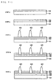
- Figs. 7-1 , 7-2 and 7-3 show the procedure of the first manufacturing method for the display panel 320.
- a step a which is a first-transparent-electrode-layer formation step
- a first transparent electrode layer 102 is formed on a substrate 101.
- a step b which is a conductivity-variable-layer formation step
- a conductivity-variable layer 103 is formed on the first transparent electrode layer 102 formed at the step a.
- the first transparent electrode layer 102 and the conductivity-variable layer 103 can be formed by forming films uniformly over the whole substrate 101, respectively.
- a step c which is a partition-member formation step
- banks 425 are formed in a predetermined pattern on the conductivity-variable layer 103 formed at the step b.
- the banks 425 can be formed by performing, for example, ink jetting, or etching and patterning. Individual pixels on the display panel 320 can be constructed by the partitions of the banks 425. Therefore, the pattern of the banks 425 can be altered in accordance with the shape of each pixel.
- an organic EL layer 410 is formed among the banks 425 formed at the step c .
- a reflection electrode 411 is first provided at a step d.
- the reflection electrode 411 can be formed by evaporating a metal such as aluminum.
- the reflection electrode 411 provided at the step d is overlaid with an ITO film 412 at a step e , a hole transport layer 413 at a step f , and an organic light emission layer 414 at a step g in succession.
- the respective layers of the reflection electrode 411, ITO film 412, hole transport layer 413 and organic light emission layer 414 can be stacked by employing ink-jet technology.
- organic light emission layers for R-light, 414R, organic light emission layers for G-light, 414G, and organic light emission layers for B-light, 414B can be formed selectively at desired positions by the ink-jet technology.
- an electron transport layer 415 is formed on the banks 425 formed at the step c , and on the organic light emission layer 414 formed at the step g .
- the organic EL layer 410 is formed at the steps d - h.
- the respective layers of the reflection electrode 411, ITO film 412, hole transport layer 413 and organic light emission layer 414 may well be fabricated by print technology based on transfer, a photo process, or the like without resorting to the ink jetting.
- a hole transport layer 413, an organic light emission layer 414, etc. which are patterned can alternatively be stacked by metal evaporations.
- a pattern which is inversely tapered in correspondence with pixels is prepared on the conductivity-variable layer 103 which is formed uniformly, whereupon the respective layers of the organic EL layer 410 are uniformly formed on inversely-tapered resist portions prepared.
- the respective layers formed on the inversely-tapered resist portions become a structure in which they are electrically isolated every resist portion, so that the organic EL layer 410 can be provided in correspondence with the respective pixels without disposing the banks 425.
- a second transparent electrode layer 104 is formed on the electron transport layer 415 formed at the step h.
- the electron transport layer 415 at the step h and the second transparent electrode layer 104 at the step i can be formed by forming films uniformly over the whole surface of the substrate 101.
- the upper surface of the second transparent electrode layer 104 formed at the step i is sealed by a protective layer 105.
- the display panel 320 of this embodiment can be manufactured. Besides, the display panel 320 dispenses with TFT elements.
- the layers of the parts except the banks 425 for constructing the pixels, and the organic EL layer 410 provided in correspondence with the pixels, can be formed by forming the films over the whole surface of the substrate 101. Therefore, the display panel 320 can be manufactured with ease.
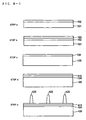
- Figs. 8-1 , 8-2 and 8-3 show the procedure of the second manufacturing method for the display panel 320.
- the second manufacturing method for the display panel 320 differs from the first manufacturing method in the point that a first layered structure and a second layered structure are fabricated as separate members, and that they are thereafter stuck to each other.
- the first layered structure is constructed of a substrate 101 being a first substrate, a first transparent electrode layer 102, and a conductivity-variable layer 103.
- a first-layered-structure formation step which consists of a step a and a step b, the first layered structure constructed of the substrate 101, first transparent electrode layer 102 and conductivity-variable layer 103 is formed.
- the step a being a first-transparent-electrode-layer formation step
- the step b being a conductivity-variable-layer formation layer are respectively the same as the step a and step b of the first manufacturing method stated before.
- the respective layers can be formed uniformly over the whole surface of the substrate 101.
- a second-layered-structure formation step which consists of a step c - a step i , there is formed the second layered structure which is constructed of a protective layer 105 being a second substrate, a second transparent electrode layer 104, banks 425 being partition members, and an organic EL layer 410.
- respective layers are stacked successively from the protective layer 105, reversely to the step d - the step j in the procedure of the first manufacturing method.
- the step c which is a second-transparent-electrode-layer formation step, the second transparent electrode layer 104 is formed on the protective layer 105.
- the protective layer 105 is a parallel flat plate which is made of an optically transparent member.
- an electron transport layer 415 is provided on the second transparent electrode layer 104 formed at the step c .
- the second transparent electrode layer 104 at the step c , and the electron transport layer 415 at the step d can be formed uniformly over the whole surface of the protective layer 105.
- the banks 425 are provided in a predetermined pattern on the electron transport layer 415 provided at the step d.
- the formation of the banks 425 is the same as that in the first manufacturing method.
- an organic light emission layer 414, a hole transport layer 413, an ITO film 412 and a reflection electrode 411 are successively stacked among the banks 425 formed at the step e.
- the organic EL layer 410 is constructed of the electron transport layer 415 which has been formed at the step d, and the organic light emission layer 414, hole transport layer 413, ITO film 412 and reflection electrode 411 which have been formed at the step f - the step i.
- the respective layers of the organic EL layer 410 are stacked successively from the side of the protective layer 105.
- the details of the stacking of the respective layers of the organic EL layer 410 are the same as the procedure at the steps d - j of the first manufacturing method. In this way, the second layered structure corresponding to pixels can be formed at the second-layered-structure formation step.
- a bonding layer 850 being electrically conductive is provided on the reflection electrode 411 formed at the step i.
- the second layered structure formed at the second-layered-structure formation step is stuck onto the first layered structure formed at the first-layered-structure formation step, into a unitary structure as the display panel 320.
- the first and second layered structures are stuck together so that the conductivity-variable layer 103 of the first layered structure, and the banks 425 as well as the bonding layer 850 of the second layered structure may be placed on each other.
- the bonding layer 850 When the bonding layer 850 has intruded between the bank 425 and the conductivity-variable layer 103 at the step k, the parts of the reflection electrode 411 corresponding to the adjacent pixels are electrically connected with each other by the bonding layer 850 having intruded. When the parts of the reflection electrode 411 corresponding to the adjacent pixels are electrically connected with each other, it becomes difficult to control the drive of the display panel 320 in accordance with an image signal.
- the bonding layer 850 needs to be prevented from intruding between the banks 425 and the conductivity-variable layer 103.
- the bonding layer 850 should desirably be provided on only regions surrounded with the banks 425, by employing ink jetting. In this way, the bonding layer 850 is prevented from intruding between the banks 425 and the conductivity-variable layer 103, and the display panel 320 which can be precisely controlled in accordance with the image signal is obtained.
- an organic EL display In a case where an organic EL display is provided with TFT elements, it needs to be manufactured so that the positions of the electrodes of the TFT elements may be registered with the positions of the parts of an organic EL layer corresponding to pixels.
- the display panel 320 dispenses with the TFT elements.
- the organic EL layer 410 need not have its positions registered as in the case of providing the TFT elements, but it may well be constructed in correspondence with the pixels, on the conductivity-variable layer 103 formed over the whole surface of the substrate 101. Therefore, the first layered structure which can be formed over the whole surface of the substrate 101, and the second layered structure which structurally corresponds to the pixels can be respectively formed as the separate members. Besides, the first layered structure and the second layered structure are stuck together into the unitary structure, whereby the display panel 320 can be manufactured.
- the second layered structure When the second layered structure is formable as the member separate from the first layered structure, it can be formed by successively stacking the second transparent electrode layer 104 and the organic EL layer 410 on the protective layer 105.
- the protective layer 105 can be made a more rigid member than in the case of forming the protective layer 105 on a layered structure corresponding to pixels. Therefore, this manufacturing method brings forth the advantage that the protective layer 105 of the display panel 320 can be made rigid, so the manufactured display panel 320 can be used for a long term.
- a method in which a plurality of unitized display panels are arrayed in the shape of tiles may well be adopted as a method of manufacturing a large-sized display panel 320.
- the display panel 320 of large size and high definition can be manufactured with ease.
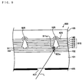
- Fig. 9 shows the schematic construction of a display panel 920 according to Embodiment 3 of the present invention.
- the same signs are assigned to the same portions as in the display apparatus 300 of the foregoing embodiment 2, and they shall not be repeatedly described.
- the display panel 920 in this embodiment features that the region of a reflection electrode 911 corresponding to each pixel is larger than the region of the part of an organic EL layer 910 as is partitioned by banks 925.
- the organic EL layer 910 is constructed of the reflection electrode 911, an ITO film 412, a hole transport layer 413, an organic light emission layer 414 and an electron transport layer 415.
- the reflection electrode 911 can be constructed by evaporating a metal, for example, aluminum (Al).
- the bank 925 is an electrical insulating member which is provided to be rectilinear in two directions being substantially orthogonal to each other, on a region in a plane being substantially parallel to the substrate 101.
- the banks 925 can be formed by subjecting polyimide, for example, to ink jetting or to etching and patterning.
- each of the banks 925 has such a shape that, as shown in Fig. 9 , the peripheral parts 911a of the reflection electrode 911 lie in two places near the base of a substantially equilateral- triangular shape.
- the ITO film 412, hole transport layer 413, organic light emission layer 414 and electron transport layer 415 which are the portions of the organic EL layer 910 other than the reflection electrode 911, are divided into regions corresponding to a plurality of pixels by the parts of the slanting surfaces of the banks 925 in the substantially equilateral-triangular shape.
- the reflection electrode 911 is provided so that the peripheral parts 911a thereof may be held between the banks 925 and the regions 903a of a conductivity-variable layer 103. Therefore, when the reflection electrode 911 is viewed from the side of a protective layer 105, it has the region which is larger than the region of the organic EL layer 910 divided by the slanting surface parts of the banks 925.
- control light L has entered the region 903a of the conductivity-variable layer 103 as shown in Fig. 9 .
- the region of the bank 925 occupies the position of the peripheral part 911a, a voltage cannot be sufficiently applied to the reflection electrode 911 even in a case where the conductivity of the region 903a has been changed by the control light L. Therefore, the control light L cannot satisfactorily contribute to the drive of the display panel 920.
- the region of the reflection electrode 911 is made larger in correspondence with the region of the peripheral part 911a, the voltage can be sufficiently applied to the reflection electrode 911 in the case where the conductivity of the region 903a has been changed by the control light L. Accordingly, the control light L having entered the region 903a can satisfactorily contribute to the drive of the display panel 920.
- the region of the reflection electrode 911 provided in correspondence with each pixel is enlarged, whereby the control light L having entered a larger area than in the case where the reflection electrode 911 is divided into the region of the same size as that of the region of the organic EL layer 910 can be utilized, so that the utilization efficiency of the control light L is enhanced.
- the control light L having entered the larger area can be utilized, the control of the display panel 920 can be satisfactorily performed even when the entrance position of the control light L is difficult to be controlled at a high precision.
- each bank 925 is located in the space between the adjacent parts of the reflection electrode 911 as in this embodiment, whereby the parts of the reflection electrode 911 corresponding to the adjacent pixels can be prevented from being electrically connected with each other.
- the display panel 920 can be precisely controlled in accordance with the image signal.
- Fig. 10 shows the schematic construction of a display panel 1020 according to Embodiment 4 of the present invention.
- the same signs are assigned to the same portions as in the display apparatus 300 of the foregoing embodiment 2, and they shall not be repeatedly described.
- the display panel 1020 features that a conductivity-variable layer 1003 has a structure in which it is divided into a plurality of regions corresponding to pixels.
- the details of this embodiment are the same as in the foregoing embodiment 2 except the point that, likewise to an organic EL layer 410, the conductivity-variable layer 1003 is divided in correspondence with the pixels by banks 425.
- a manufacturing method for the display panel 1020 is the same as the manufacturing method for the foregoing display panel 320 except the point that the banks 425 are provided on a first transparent electrode layer 102, whereupon the conductivity-variable layer 1003 is stacked on the first transparent electrode layer 102 partitioned by the banks.
- the conductivity-variable layer 1003 tends to spread a region where its conductivity changes, to the surroundings around the irradiation position of control light L in proportion to the intensity of the control light L and the irradiation time period thereof.
- the conductivity-variable layer 1003 is divided into the plurality of regions in correspondence with the pixels, whereby the parts of an organic light emission layer 414 corresponding to predetermined pixels can be precisely caused to emit light by the control light L.
- the display panel 1020 can be satisfactorily controlled. This brings forth the advantage that the drive of the display panel 1020 can be precisely controlled.
- Fig. 11 shows the schematic construction of a display apparatus 1100 according to Embodiment 5 of the present invention.
- the same signs are assigned to the same portions as in the display apparatus 300 of the foregoing embodiment 2, and they shall not be repeatedly described.
- An optical system for control lights, 1140 in the display apparatus 1100 features that it has two light source units for the control lights, 1150 and 1160.
- the light source unit for the control lights, 1150 includes a first light source portion for the control light, 1151, a second light source portion for the control light, 1152 and a third light source portion for the control light, 1153.
- the first light source portion for the control light, 1151 supplies first control light L4 to the part of a first transparent electrode layer 102 (refer to Fig.
- the second light source portion for the control light, 1152 supplies second control light L5 to the part of the first transparent electrode layer 102 (refer to Fig. 4 ) corresponding to a pixel for G-light, 420G.
- the third light source portion for the control light, 1153 supplies third control light L6 to the part of the first transparent electrode layer 102 (refer to Fig. 4 ) corresponding to a pixel for B-light, 420B.
- the control lights L4, L5 and L6 scan the first region 1121 of a display panel 1120 by galvanomirrors 1154, 1155 and 1156 which are disposed in correspondence with the light source portions for the respective control lights, 1151, 1152 and 1153.
- the light source unit for the control lights, 1160 includes a first light source portion for the control light, 1161, a second light source portion for the control light, 1162 and a third light source portion for the control light, 1163.
- the first light source portion for the control light, 1161 supplies first control light L7 to the part of the first transparent electrode layer 102 (refer to Fig. 4 ) corresponding to a pixel for R-light, 420R.
- the second light source portion for the control light, 1162 supplies second control light L8 to the part of the first transparent electrode layer 102 (refer to Fig. 4 ) corresponding to a pixel for G-light, 420G.
- the third light source portion for the control light, 1163 supplies third control light L9 to the part of the first transparent electrode layer 102 (refer to Fig. 4 ) corresponding to a pixel for B-light, 420B.
- the control lights L7, L8 and L9 scan the second region 1122 of the display panel 1120 by galvanomirrors 1164, 1165 and 1166 which are disposed in correspondence with the light source portions for the respective control lights, 1161, 1162 and 1163.
- the light source units for the control lights, 1150 and 1160 supply the control lights L4 - L6 and L7 - L9 to the first region 1121 and second region 1122 being the different regions of the display panel 1120, respectively.
- the light source units for the control lights, 1150 and 1160 supply the respective control lights L4 - L6 and L7 - L9 while taking charge of the different regions of the display panel 1120. It is therefore possible to shorten distances from the individual galvanomirrors 1154, 1155, 1156, 1164, 1165 and 1166 to the display panel 1120. Moreover, since the light source units supply the control lights L4 - L9 while taking charge of the different regions of the display panel 1120, the scanning angles of these control lights L4 - L9 can be narrowed. Since the scanning distances of the control lights L4 - L9 are shortened, an image can be satisfactorily displayed even when the scanning speeds of the control lights L4 - L9 are lowered.
- control lights L4 - L9 can be allowed to scan with ease.
- the display apparatus 1100 of this embodiment employs the two light source units for the control lights, 1150 and 1160, control lights may well be supplied by disposing three or more light source units for the control lights and dividing the display panel 1120 into three or more regions.
- Fig. 12 shows the schematic construction of a display apparatus 1200 which is a modification to the display apparatus 1100 of this embodiment.
- the display apparatus 1200 features that three galvanomirrors 1254, 1255 and 1256 are disposed.
- First control lights L4 and L7 from first light source portions for the control lights, 1151 and 1161 in light source units for control lights, 1150 and 1160 scan a first region 1121 and a second region 1122 by the galvanomirror 1254, respectively.
- Second control lights L5 and L8 from second light source portions for the control lights, 1152 and 1162 scan the first region 1121 and the second region 1122 by the galvanomirror 1255, respectively.
- Third control lights L6 and L9 from third light source portions for the control lights, 1153 and 1163 scan the first region 1121 and the second region 1122 by the galvanomirror 1256, respectively. Owing to the construction in which each single galvanomirror allows the plurality of control lights to scan in this manner, the number of components can be decreased.
- the organic EL layer is employed for the display panel in each of the foregoing embodiments, the present invention is not restricted thereto as long as light is emitted by applying a voltage.
- the organic EL layer may well be replaced with an inorganic EL layer.
- the display apparatus performs an analog control which displays a continuous change magnitude by the control light L modulated in accordance with the image signal.
- a digital control may well be performed using the control light L.
- only two discontinuous values may well be taken in accordance with the ON and OFF states of the control light L, so as to represent a gradation by employing subframe drive.
- a display apparatus is useful for presentation and in case of displaying a dynamic image, and it is suited especially in the case of displaying a projection image.
Description
- The present invention relates to a display panel, a method of manufacturing a display panel, and a display apparatus, and more particularly to the technology of a display panel for use in a display apparatus which is controllable by light.
- Heretofore, an organic electroluminescence (hereinbelow, termed "EL") display, for example, has been employed as an image display apparatus. As the technology of the organic EL display, there has been, for example, one proposed in "Organic EL materials and Displays", CMC, ISBN: 4-88231-284-0 C3054, Chapter 19, "Driving method for Organic EL display", Shingo Kawashima, pp. 279-289
- The organic EL display in the prior art is such that thin film transistor (hereinbelow, termed "TFT") elements made from low-temperature poly-silicon, amorphous silicon or the like are disposed in regions which correspond respectively to pixels. Each TFT element has its ON/OFF state controlled by access which employs current. The organic EL display can be driven in such a way that the ON/OFF states of the respective TFT elements are controlled by employing currents. In a case of increasing the number of pixels, however, when the TFT element is provided for every pixel, also the number of TFT elements increases in accordance with the increase of the number of pixels. When the number of TFT elements increases, also the number of electrical wiring lines for accessing the TFT elements with currents increases. It can form a cause for the decrease of a yield that the construction of the organic EL display becomes complicated. Accordingly, when the number of pixels is increased in order to enlarge the size of a screen, the manufacturing cost of the organic EL display rises suddenly in some cases.
- Since the increase of the number of TFT elements results in increasing also the number of electrical wiring lines, it can form a cause for incurring the increase of an electrical resistance. When the electrical resistance increases, it becomes difficult to make the accesses by causing sufficient currents to pervade all the TFT elements. Further, it is very difficult to manufacture a large-sized screen which is free from the dispersion of the TFT elements. When the TFT elements of the screen disperse, a display image becomes nonuniform. In this manner, the uniform manufacture of the TFT elements is difficult in addition to the possible sudden rise of the manufacturing cost, so that the manufacture of the large-sized screen is difficult. Thus, the prior-art organic EL display is problematic in the case of enlarging the size of the screen, because of the difficulty in the driving aspect in the accesses to the TFT elements, and the difficulty in the manufacturing aspect.
-
EP 0382642 discloses a monochromatic display device comprising, on a substrate, an electroluminescent layer and a photoconductive layer which are stacked up. This stack is interposed between two electrode systems serving to excite the electroluminescent layer, the electroluminescent layer having an emission spectrum encompassing the sensitivity spectrum of the photoconductive material. An optical filter is arranged between the electroluminescent layer and the observer of the device and lets through that portion of the emission spectrum of the electroluminescent layer most useful to the display. The optical filter blocks a region of the emission spectrum of the ambient lighting, the sensitivity spectrum of the photoconductive layer then essentially being contained in this region. -
US 5200668 discloses an injection type thin film luminescence element having two electrode layers at least one of which is transparent or translucent, and having between these two electrode layers a luminescence function-manifesting layer comprising a laminated layer of a p-type or n-type inorganic semiconductor thin film layer and an organic compound thin film layer. -
US 5539424 discloses a thin-film EL display device of red luminescent color. The thin-film EL display device has a first transparent electrode, a first transparent insulating layer, a light-emitting layer of zinc sulfide (ZnS) with the addition of manganese (Mn), a red-light transmitting filter of amorphous silicon (a-Si), a second transparent insulating layer, and a second transparent electrode, which are successively deposited one on top of another on a glass substrate. The EL display device produces red light from orange light emission from the light-emitting layer. -
US 2002/167268 discloses a color display substrate, having plural color display elements arranged in a matrix pattern, and a manufacturing method for obtaining a color filter substrate and color luminescent substrate. The manufacturing method of a color display substrate includes the step of forming plural color dots by selectively ejecting liquid droplets from nozzles in accordance with input data. The plural color dots constitute plural pixels, which constitute plural color filter elements arranged in a matrix pattern. The plural color dots have a first dot pitch in a direction perpendicular to a first base line. Each of the plural color dots is formed to lie at a distance of at least substantially an integral multiple of the first dot pitch from the first base line. - The present invention has been made in view of the above problems, and it has for its object to provide a display panel easy of enlarging a size, a method of manufacturing the display panel, and a display apparatus employing the display panel.
- In order to solve the above problems and to accomplish the object, according to a first aspect of the present invention, there is provided a display panel as defined in claim 1.
- The display panel of the present invention is driven by entering the control light into the first transparent electrode layer.
- When the control light is not entered, the conductivity-variable layer functions as an insulating layer whose electrical conductivity is substantially zero. Besides, when the control light is entered, the conductivity-variable layer has its electrical conductivity changed in accordance with the light quantity of the control light transmitted through the first transparent electrode layer. The conductivity-variable layer controls the voltage applied to the electroluminescent layer when a voltage is applied between the first and second transparent electrode layers, in response to the quantity of control light entering the conductivity-variable layer. The voltage corresponding to the light quantity of the control light is applied to the EL layer, whereby this EL layer emits the light in correspondence with the light quantity of the control light. In this way, the display panel can have its drive controlled by accessing it with the control light (light addressing). Since the display panel of the present invention is controllable by entering the control light thereinto, it need not be provided with TFT elements. Whereas the TFT elements need to be disposed in respective regions corresponding to pixels, the conductivity-variable layer, first transparent electrode layer and second transparent electrode layer can be formed by forming films uniformly over the whole substrate, so that the display panel of the present invention can be manufactured with ease. Moreover, the respective pixels can be accessed by the construction which allows the control light to scan, so that they need not be electrically accessed. For this reason, electrical wiring lines need not be laid for the respective pixels. Therefore, the display panel of the present invention can be made simpler in construction than a prior-art EL display. Owing to the simplified construction of the display panel, the yield thereof can be increased to curtail a manufacturing cost.
- With the TFT elements, as the number of pixels increases by enlarging the size of a screen, it becomes difficult to manufacture a display which is free from the dispersion of the TFT elements. Besides, with the enlargement of the size of the screen and the increase of the number of pixels, also wiring lines for electrically connecting the TFT elements increase, and hence, there is the problem that an electrical resistance increases. In contrast, the display panel of the present invention can be manufactured by chiefly forming the films of materials constituting the respective layers, uniformly over the whole substrate, so that even a large-sized screen is easy of manufacture. Besides, the display panel of the present invention need not electrically access the respective pixels, so that an electrical resistance does not increase even when the number of pixels is increased. Since the electrical resistance is not increased even by the increase of the number of pixels, even a large-sized display panel can have its drive controlled with ease as long as the control light can be entered into the whole display panel. Further, owing to the non-increase of the electrical resistance and also to the low dissipation power of the EL layer itself, dissipation power in the case of enlarging the size of the display panel can be decreased. Thus, the display panel easy of enlarging the size is obtained.
- Besides, according to a preferable aspect of the present invention, a display panel should desirably comprise an optical system for control light, which is adapted to supply the control light to said display panel; and a light shield portion which is provided near a surface of said first electrode layer at which the control light from the optical system enters the display panel, and which is formed with openings in correspondence with the pixels; wherein each of the openings is arranged at a position through which the control light from the optical system passes, so that the control light enters the first electrode layer at a position corresponding to a predetermined one of the pixels; and the electroluminescent layer is adapted to emit light at the region corresponding to the predetermined pixel in response to the control light.
- After having passed through the openings provided in the light shield portion, the control light is entered into the first transparent electrode layer. Each of the openings is arranged at the position through which the control light is passed to be entered into the part of the first transparent electrode layer corresponding to the predetermined pixel. Thus, the control light can be entered into only the part of the first transparent electrode layer corresponding to the predetermined pixel.
- In a case where the control light has proceeded toward the part of the first transparent electrode layer corresponding to any pixel different from the predetermined pixel, it is intercepted by the light shield portion. In this manner, the light shield portion and the openings corresponding to the pixels are provided, whereby the control light can be prevented from erroneously entering the region which corresponds to the pixel other than the predetermined pixel. Besides, in a case where a plurality of control lights are entered into regions which correspond to pixels different from one another, it is allowed to employ a construction in which the plurality of control lights are passed through one opening. On this occasion, the control lights are allowed to scan at a precision enough to enter into the opening, whereby the control lights can be precisely entered into only the parts of the first transparent electrode layer corresponding to predetermined pixels even when the entrance positions of the control lights are not controlled at a still higher precision. Moreover, since the scanning speed of the control lights need not be made slow, the light addressing can be precisely performed without degrading the quality of an image. Thus, a precise control can be performed with ease.
- The EL layer has a structure in which it is divided into a plurality of regions corresponding to the pixels, preferably by a plurality of partition members provided on the conductivity-variable layer. The EL layer is made the structure in which it is divided into the plurality of pixels, by providing the partition members on the conductivity-variable layer. Thus, it is possible to obtain a display panel which can emit light for the respective pixels in accordance with an image signal, so as to display an image.
- Herein, when the control light has entered the position of the first transparent electrode layer corresponding to the partition member, the conductivity-variable layer has its conductivity changed only under the partition member. When the conductivity of the conductivity-variable layer changes only under the partition member, it is sometimes impossible to apply a sufficient voltage to the EL layer, so the EL layer fails to emit light. Here, since the display panel of the present invention dispenses with TFT elements, electric wiring lines need not be laid under the partition members. Therefore, the regions of the reflection electrode can be spread to spaces underlying the partition members.
- When the peripheral part of the reflection electrode is provided so as to be held between the partition members and the conductivity-variable layer, the region of the reflection electrode corresponding to each pixel becomes larger than the part of the EL layer divided into pixels by the partition members, to the amount of a region held between the partition members and the conductivity-variable layer. Since the region of the reflection electrode corresponding to each pixel is larger than the region of the part of the EL layer divided by the partition members, it is possible to utilize the control light which has entered a larger area than in the case where the reflection electrode is divided in correspondence with the pixels similarly to the EL layer. Besides, since the control light having entered the larger area can be utilized, the control of the display panel can be satisfactorily performed even when it is difficult to control the entrance position of the control light at a high precision. Thus, the EL layer can be efficiently caused to emit light.
- Besides, as a preferable aspect of the present invention, the conductivity-variable layer should desirably have a structure in which it is divided into a plurality of regions corresponding to the pixels. A region in which the conductivity of the conductivity-variable layer changes, tends to spread to the surroundings around the irradiation position of the control light in proportion to the intensity of the control light and the irradiation time period thereof. When the conductivity-variable layer is made the structure in which, likewise to the structure of the EL layer, it is divided into the plurality of regions corresponding to the pixels, the parts of the EL layer corresponding to predetermined pixels can be precisely caused to emit light by the control light. Moreover, even when it is difficult to control the entrance position of the control light at a high precision, the control of the display panel can be satisfactorily performed. Thus, a display panel capable of precise control is obtained.
- Besides, as a preferable aspect of the present invention, it is desirable that the plurality of regions of the EL layer are provided in correspondence with pixels for first color light, pixels for second color light, and pixels for third color light; that each pixel aggregate is constructed of one of the pixels for the first color light, one of the pixels for the second color light, and one of the pixels for the third color light; and that a plurality of such pixel aggregates are provided at substantially equal intervals in two predetermined directions being substantially orthogonal to each other. A full-color image is displayed by the pixels for the first color light, the pixels for the second color light, and the pixels for the third color light. When each pixel aggregate is constructed of the pixel for the first color light, the pixel for the second color light, and the pixel for the third color light, the pixels can be densely arrayed. When the pixels can be densely arrayed, the aperture percentage of the display panel is enhanced, and a bright image is obtained. Further, since the plurality of pixel aggregates are arrayed at the substantially equal intervals in the two-dimensional directions, the distortion of an image can be reduced to precisely display the image. Thus, a bright and precise full-color image is obtained.
- Further, according to a second aspect of the present invention, there is provided a method of manufacturing a display panel as defined in
claim 6. - Thus, the display panel stated before can be manufactured. Besides, since the display panel stated before dispenses with TFT elements, the layers of parts, which are other than the partition members for defining the pixels and the EL layer provided in correspondence with the pixels, can be formed by forming films over the whole surface of the substrate. Therefore, the display panel can be manufactured with ease.
- Further, according to a third aspect of the present invention, there is provided a method of manufacturing a display panel as defined in claim 7.
- In a case where a display panel is provided with TFT elements, it needs to be manufactured so that the positions of the electrodes of the TFT elements may be registered with the positions of an EL layer corresponding to pixels. In contrast, the display panel stated before dispenses with the TFT elements. The EL layer need not have its positions registered as in the case of providing the TFT elements, and it may well be constructed in correspondence with pixels, on the conductivity-variable layer formed over the whole surface of the first substrate. Therefore, the first layered structure which is formable over the whole surface of the first substrate, and the second layered structure which has the structure corresponding to the pixels can be respectively formed as separate members. Besides, the first layered structure and the second layered structure are stuck to each other into the unitary structure, whereby the display panel can be manufactured. In this case, the second layered structure can be formed by successively stacking the second transparent electrode layer and the EL layer on the second substrate. When the second layered structure can be formed by successively stacking the respective layers on a protective layer which is the second substrate, the protective layer can be made a more rigid member than in a case of forming the protective layer on the layered structure which corresponds to the pixels. According to the present invention, the protective layer of the display panel can be made rigid, so that the manufactured display panel can be used for a long term.
- Preferably, there is provided a display apparatus as defined in claim 8. The display apparatus of the present invention is controlled by entering the control light from the optical system for the control light. The voltage for causing the EL layer to emit light is applied between the first transparent electrode layer and the second transparent electrode layer. Since the voltage for causing the EL layer to emit light is applied by the power source, the intensity of the control light may be to the extent of changing the electrical conductivity of the conductivity-variable layer. Therefore, the optical system for the control light can be used for the display apparatus of the present invention even when it is difficult of generating control light of high intensity. Since the control light of high intensity need not be generated, the display apparatus can be used safely. Besides, since the display panel stated before is used, dissipation power is low, and the enlargement of the size of the display panel is easy.
- Further, the optical system for the control light scans the first transparent electrode layer with the control light of beam shape. The display apparatus of the present invention does not require a vacuum tube as in, for example, a display apparatus employing a CRT, so that it can be made light in weight even when the display panel is made large in size. Moreover, unlike in a case of employing an electron beam, the control light can have its proceeding direction deflected by a mirror and can be fined by a lens. Therefore, even when the display apparatus is thinned, the control light can scan over the whole large-sized display panel by, for example, bending the proceeding direction of the control light with a mirror. Further, by bending the proceeding direction of the control light, the optical path of the control light becomes long with the display apparatus kept small in size. Therefore, the scanning angle of the control light can be narrowed. Thus, a display apparatus capable of easily enlarging the size of the display panel is obtained.
- Besides, as a preferable aspect of the present invention, it is desirable that the optical system for the control light includes a plurality of light source units for the control lights; that each of the light source units for the control lights consists of a first light source portion to supply first control light to a part of the first transparent electrode layer corresponding to a pixel for first color light, a second light source portion to supply second control light to a part of the first transparent electrode layer corresponding to a pixel for second color light, and a third light source portion to supply third control light to a part of the first transparent electrode layer corresponding to a pixel for third color light; and that the plurality of light source units for the control lights supply the first control light, the second control light and the third control light to different regions of the display panel, respectively.
- The control lights are supplied in such a way that the respective light source units for the control lights take charge of the different regions of the display panel, whereby distances from galvanomirrors to the display panel can be shortened. Moreover, the control lights are supplied by allotting the different regions of the display panel to the light source units, whereby the scanning angles of the control lights can be narrowed. Since the scanning distances of the control lights are shortened, an image display can be satisfactorily performed even when the scanning speeds of the control lights are lowered. Thus, the display apparatus can be made small in size, and besides, the control lights can be easily allowed to scan.
- Besides, as a preferable aspect of the present invention, it is desirable to include a frame in which at least the optical system for the control light is accommodated; wherein the display panel is mounted on the frame. Since the display panel stated before is mounted on the frame, the frame can be made light in weight and thin in structure even when the display panel is enlarged in size. Thus, a display apparatus which is easy of enlarging the size of the display panel is obtained.
- Besides, as a preferable aspect of the present invention, it is desirable that light from another image display apparatus is employed as the control light. The display panel is arranged with the first transparent electrode layer thereof held in opposition to the display of the other image display apparatus, and the light from the display is entered into the first transparent electrode layer of the display panel as the control light. The conductivity-variable layer has its conductivity changed in accordance with the light quantity of the light from the display, at its position corresponding to that position of the first transparent electrode layer into which the light from the display has been entered. Therefore, even in a case where the EL layer is provided uniformly over the whole surface of the display panel, it can be caused to emit light in accordance with the position and light quantity of the light from the display as has been entered into the first transparent electrode layer, thereby to display an image. In this way, the display panel can be driven by entering the light from the display into the first transparent electrode layer.
- Further, color filters are provided on the entrance side of the display panel for the light from the display and on the exit side of the display panel for the emitted light, whereby a full-color image can be obtained in the display panel. Thus, a display panel capable of displaying the image of the other image display apparatus is obtained with the simple construction.
- Embodiments of the present invention will now be described by way of further example only and with reference to the accompanying drawings, in which:-
-
Fig. 1 is a schematic constructional view of a display apparatus according to Embodiment 1 of the present invention. -
Fig. 2-1 is an explanatory view of an example of use of a display panel. -
Fig. 2-2 is an explanatory view of a construction in which the image of a display is displayed on a display panel. -
Fig. 3 is a schematic constructional view of a display apparatus according toEmbodiment 2 of the present invention. -
Fig. 4 is a schematic constructional view of a display panel and an optical system for control lights. -
Fig. 5 is an explanatory view of the relationship between openings and the optical system for the control lights. -
Fig. 6-1 is an explanatory view of a layout example of individual pixels for color lights. -
Fig. 6-2 is an explanatory view of a layout example of individual pixels for color lights. -
Fig. 6-3 is an explanatory view of a layout example of individual pixels for color lights. -
Fig. 7-1 is an explanatory view of the procedure of a first manufacturing method for the display panel. -
Fig. 7-2 is an explanatory view of the procedure of the first manufacturing method for the display panel. -
Fig. 7-3 is an explanatory view of the procedure of the first manufacturing method for the display panel. -
Fig. 8-1 is an explanatory view of the procedure of a second manufacturing method for the display panel. -
Fig. 8-2 is an explanatory view of the procedure of the second manufacturing method for the display panel. -
Fig. 8-3 is an explanatory view of the procedure of the second manufacturing method for the display panel. -
Fig. 9 is a schematic constructional view of a display panel according to Embodiment 3 of the present invention. -
Fig. 10 is a schematic constructional view of a display panel according to Embodiment 4 of the present invention. -
Fig. 11 is a schematic constructional view of a display apparatus according to Embodiment 5 of the present invention. -
Fig. 12 is a schematic constructional view of a display apparatus according to a modification to Embodiment 5. -
Fig. 1 shows the schematic construction of adisplay apparatus 100 according to Embodiment 1 of the present invention. In this embodiment, the construction of thedisplay apparatus 100 and a control by control light will be first described, and practicable image displays based on thedisplay apparatus 100 will be subsequently described. Thedisplay apparatus 100 is constructed of adisplay panel 120, apower source 130, and an optical system for control light, 140. Thedisplay panel 120 displays an image by causing anorganic EL layer 110 to emit light. - A
substrate 101 is a parallel flat plate which is made of a glass member, a polymer member or the like which is optically transparent. A firsttransparent electrode layer 102 being optically transparent, and a conductivity-variable layer 103 are successively stacked on thesubstrate 101. The firsttransparent electrode layer 102 can be made of an ITO film. The conductivity-variable layer 103 has its electrical conductivity changed by the control light L transmitted through the firsttransparent electrode layer 102. Amorphous silicon (hereinbelow, termed "a-Si") or a photosensitive organic film, for example, can be employed for the conductivity-variable layer 103. The a-Si, for example, should desirably contain hydrogen. Besides, the a-Si is formed by chemical vapor deposition (CVD). In a state where the a-Si is not irradiated with the control light L at all, it functions as an insulating member whose electrical conductivity is substantially zero (that is, whose resistance value is infinitely large). In contrast, when the a-Si is irradiated with the control light L, the conductivity enlarges (that is, the resistance value becomes small) in accordance with the quantity of the light. That region of the conductivity-variable layer 103 in which the conductivity changes corresponds to that region of the firsttransparent electrode layer 102 which has irradiated the a-Si with the control light L. - The
organic EL layer 110 is provided on the conductivity-variable layer 103. Theorganic EL layer 110 is constructed in such a way that areflection electrode 111, anITO film 112, ahole transport layer 113, an organiclight emission layer 114 and anelectron transport layer 115 are successively stacked from the side of the conductivity-variable layer 103. Thereflection electrode 111 can be constructed by evaporating a metal, for example, aluminum (Al). TheITO film 112 is provided in order to promote the emission of charges from thereflection electrode 111 into thehole transport layer 113. A triazole derivative, for example, can be employed as the material of thehole transport layer 113. A benzothiazolic compound, for example, can be employed for the organiclight emission layer 114. An electron-transmissive compound, for example, diphenylquinone derivative can be employed for theelectron transport layer 115. Since any of thehole transport layer 113, organiclight emission layer 114 andelectron transport layer 115 has a thickness on the order of several tens nm, it is optically transparent. A secondtransparent electrode layer 104 can be made of an ITO film likewise to the firsttransparent electrode layer 102. Aprotective layer 105 which is made of an optically transparent member similar to thesubstrate 101, is provided on the secondtransparent electrode layer 104. Herein, thedisplay panel 120 has a voltage applied between the firsttransparent electrode layer 102 and the secondtransparent electrode layer 104 by thepower source 130. - As methods for stacking the individual layers which constitute the
display panel 120, it is possible to appropriately employ resistance-heating vacuum evaporation, electron-beam-heating vacuum evaporation, sputtering, ion plating, casting, spin coating, and so forth. Incidentally, the construction of theorganic EL layer 110 is not restricted to the above one. By way of example, a bonding layer may well be provided for any of the individual layers constituting theorganic EL layer 110. - Besides, a hole transport material and an electron transport material may well be mixed into the organic
light emission layer 114 by providing neither of thehole transport layer 113 and theelectron transport layer 115. If the charges of thereflection electrode 111 can be sufficiently emitted into thehole transport layer 113, theITO film 112 may well be omitted. - The optical system for the control light, 140 is constructed of a
galvanomirror 144, and a light source portion for the control light, 142. The optical system for the control light, 140 is disposed for thedisplay panel 120 and on the side of thesubstrate 101. The light source portion for the control light, 142 supplies the control light L which is beam-shaped light, for example, laser light. By way of example, a semiconductor laser element or a surface-light-emission laser element which is furnished with a modulator can be employed for the light source portion for the control light, 142. Herein, the light source portion for the control light, 142 can modulate the intensity of the control light L in accordance with an image signal from acontrol portion 148, so as to supply the modulated light. The control light L from the light source portion for the control light, 142 is reflected toward thedisplay panel 120 by thegalvanomirror 144. Besides, the control light L reflected toward thedisplay panel 120 enters that surface of thedisplay panel 120 which lies on the side of thesubstrate 101. Thegalvanomirror 144 can be fabricated by, for example, MEMS (Micro Electro Mechanical Systems) technology. Thegalvanomirror 144 turns about two predetermined axes being substantially orthogonal to each other, thereby allowing the control light L to scan in two directions. The turning of thegalvanomirror 144 is controlled in accordance with the image signal by thecontrol portion 148. In this way, the optical system for the control light, 140 scans that surface of thedisplay panel 120 which lies on the side of thesubstrate 101 with the control light L. - Employed as the control light L is light in a wavelength region which is capable of changing the electrical conductivity of the conductivity-
variable layer 103. On this occasion, in a case where the control light L has a wavelength region which is adapted to change the electrical conductivity of the conductivity-variable layer 103 most efficiently, the control light L in a small light quantity can be employed. Besides, even in a case where the control light L is in a wavelength region which is not the wavelength region adapted to change the electrical conductivity of the conductivity-variable layer 103 most efficiently, it can be employed for the control of thedisplay panel 120 by enlarging the light quantity of the control light L. Thus, thedisplay panel 120 can be controlled by appropriately combining the wavelength and light quantity of the control light L. Any of an ultraviolet laser, a visible radiation laser and an infrared laser can be employed for the control light L. Besides, not only the laser light, but also the beam-shaped light, for example, light from a light emitting diode element (LED) may well be employed as the control light L. - Next, the control of the
display apparatus 100 by the control light L will be described. The control light L from the optical system for the control light, 140 is transmitted through thesubstrate 101 and firsttransparent electrode layer 102 of thedisplay panel 120, and it enters the conductivity-variable layer 103. When the control light L whose intensity corresponds to an image signal has entered the conductivity-variable layer 103, the electrical conductivity of this layer increases in accordance with the light quantity of the control light L as to the part thereof at the entrance position of the control light L. Incidentally, strictly speaking, a region where the conductivity of the conductivity-variable layer 103 changes tends to spread to the surroundings around the irradiation position in proportion to the intensity and irradiation time period of the control light L. Here, the control shall be discussed assuming that the control light L scans at high speed by thegalvanomirror 144, and that the conductivity changes only in and near the region irradiated with the control light L. - Owing to the increase of the conductivity of the conductivity-
variable layer 103, one electrode of thepower source 130 as is connected with the firsttransparent electrode layer 102 is electrically connected with thereflection electrode 111 via the firsttransparent electrode layer 102 and the conductivity-variable layer 103. Since the conductivity of the conductivity-variable layer 103 changes in accordance with the light quantity of the control light L transmitted through the firsttransparent electrode layer 102, a voltage corresponding to the light quantity of the control light L is applied to thereflection electrode 111. Besides, the other electrode of thepower source 130 is held connected to the secondtransparent electrode layer 104. When a voltage is applied between thereflection electrode 111 and the secondtransparent electrode layer 104, the charges of thereflection electrode 111 are emitted into thehole transport layer 113 through theITO film 112. When the charges are emitted into thehole transport layer 113, holes are transmitted from thehole transport layer 113 into the organiclight emission layer 114. Further, when the voltage is applied between thereflection electrode 111 and the secondtransparent electrode layer 104, electrons are transported from theelectron transport layer 115 into the organiclight emission layer 114. In the organiclight emission layer 114, the holes from thehole transport layer 113 combine with the electrons from theelectron transport layer 115. The fluorescent substance of the organiclight emission layer 114 is excited by energy which is generated at the combination between the hole and the electron. Herein, when the excited fluorescent substance reverts into its ground state, a fluorescence phenomenon occurs to emit light from the organiclight emission layer 114. - The light from the organic
light emission layer 114 proceeds in all directions around that position of the organiclight emission layer 114 which corresponds to the entrance position of the control light L. The light which has proceeded from the light emission position of the organiclight emission layer 114 toward theprotective layer 105, is transmitted through theelectron transport layer 115, secondtransparent electrode layer 104 andprotective layer 105 and exits from thedisplay panel 120. Besides, the light which has proceeded from the light emission position of the organiclight emission layer 114 toward thesubstrate 101 is transmitted through thehole transport layer 113 andITO film 112 and is reflected by thereflection electrode 111. The light reflected by thereflection electrode 111 is transmitted through the individual layers and proceeds toward theprotective layer 105, and it exits from thedisplay panel 120. An observer observes the light which exits from theprotective layer 105 of thedisplay panel 120. Since thereflection electrode 111 reflects the light proceeding toward thesubstrate 101, toward theprotective layer 105, the light from the organiclight emission layer 114 can be caused to efficiently exit from thedisplay panel 120. - In this manner, the
display panel 120 is provided with the conductivity-variable layer 103, and the control light L is entered into the firsttransparent electrode layer 102, whereby the voltage corresponding to the light quantity of the control light L, in the voltage applied between the firsttransparent electrode layer 102 and the secondtransparent electrode layer 104, is applied to theorganic EL layer 110. Owing to the voltage corresponding to the light quantity of the control light L, the organiclight emission layer 114 can be caused to emit the light in accordance with the image signal. By the way, in thedisplay panel 120 in this embodiment, theorganic EL layer 110 is not divided into pixels, and it is provided uniformly over the whole surface of thedisplay panel 120. As stated above, the conductivity-variable layer 103 has its conductivity changed only in and near the region irradiated with the control light L. Owing to the change of the conductivity of only the region irradiated with the control light L, when the control light L is entered into the organiclight emission layer 114, this layer can be caused to emit the light in correspondence with the entrance position of the control light L. Therefore, when the entrance positions of the control light L are controlled using the optical system for the control light, 140, the organiclight emission layer 114 can be caused to emit light on the pixel basis in accordance with the image signal, thereby to display an image (light addressing). - The voltage for causing the organic
light emission layer 114 is applied between the firsttransparent electrode layer 102 and the secondtransparent electrode layer 104 by thepower source 130. In this embodiment, in the case of performing the light addressing with the control light L, the intensity of the control light L may be to the extent of changing the electrical conductivity of the conductivity-variable layer 103. In this embodiment, the control light L of lower intensity can be employed than in a case where light is emitted for image display by directly employing the energy of the control light L. For this reason, the light source portion for the control light, 142 is usable for thedisplay apparatus 100 even when it is difficult of generating control light L of high intensity. Therefore, the light source portion for the control light, 142 whose output power is low and which is inexpensive may well be employed for the optical system for the control light, 140. Moreover, since the control light L of high intensity need not be generated, the safety of thedisplay apparatus 100 can be enhanced. Further, thedisplay apparatus 100 of this embodiment can use visible radiation or the like as the control light L. Since an electron beam, for example, need not be employed as the control light L, a vacuum tube or the like member as in a display apparatus including a CRT is not required. Since the vacuum tube or the like member is not required, thedisplay apparatus 100 can be made light in weight even when thedisplay panel 120 is enlarged in size. This brings forth the advantage that thedisplay apparatus 100 which can easily enlarge the size of thedisplay panel 120 is obtained. - The
display apparatus 100 controls the drive of thedisplay panel 120 with the control light L. Accordingly, thedisplay panel 120 in this embodiment need not be provided with TFT elements. Whereas the TFT elements need to be disposed for the respective pixels, the conductivity-variable layer 103, firsttransparent electrode layer 102,organic EL layer 110 and secondtransparent electrode layer 104 of thedisplay panel 120 can be formed by forming films uniformly over thewhole substrate 101, respectively. Therefore, patterning is unnecessary in the manufacturing process of thedisplay panel 120, so that the manufacture of thedisplay panel 120 is easier than in the case of providing the TFT elements. Moreover, the respective pixels can be accessed by the construction which scans with the control light L, so that they need not be electrically accessed. Since the respective pixels need not be electrically accessed, electrical wiring lines need not be laid for the respective pixels. Therefore, thedisplay panel 120 in this embodiment can be made simpler in construction than the prior-art EL display. Owing to the simplified construction of thedisplay panel 120 and also the easy manufacture thereof, the yield thereof can be improved to curtail a manufacturing cost. - Since the
display panel 120 can be manufactured by forming the materials of the respective layers into the films uniformly over thesubstrate 101, the manufacture is easy even in the case of enlarging the size of thedisplay panel 120. Besides, when the TFT elements are employed, the number of wiring lines for electrically connecting the TFT elements increases with the enlargement of the size of a screen. Therefore, the employment of the TFT elements poses the problem that an electrical resistance increases with the enlargement of the size of the screen. In contrast, thedisplay panel 120 in this embodiment dispenses with the electrical accesses to the respective pixels, so that an electrical resistance is not increased even by increasing the number of pixels. Since the electrical resistance does not increase, even a large-sized display panel 120 can have its drive easily controlled as long as the control light L can be entered into thewhole display panel 120 by the optical system for the control light, 140. Besides, a PDP (plasma display panel), for example, dissipates more power with the enlargement of its size. When thedisplay panel 120 is compared with the PDP, theorganic EL layer 110 dissipates low power even in the case of enlarging the size. In this manner, the electrical resistance does not increase, and besides, the dissipation power of theorganic EL layer 110 itself is low, the dissipation power of thedisplay apparatus 100 can be lowered even in the case of enlarging the size of thedisplay panel 120. This brings forth the advantage that thedisplay panel 120 which is easy of enlarging its size is obtained. - Next, image displays based on the
display apparatus 100 of this embodiment will be concretely described. In thedisplay panel 120 of thedisplay apparatus 100, theorganic EL layer 110 is not divided into pixels, and it is provided uniformly over the whole surface of thedisplay panel 120. When light addressing is performed using the optical system for the control light, 140, thedisplay panel 120 displays a monochromatic image of identical color by light which has a wavelength corresponding to energy generated when the fluorescent substance excited by the organiclight emission layer 114 reverts into its ground state. Thedisplay panel 120 is used for thedisplay apparatus 100 which displays the image by using the optical system for the control light, 140 in this manner, and it can also be used for loading the image of the display of another image display apparatus thereinto and then displaying the loaded image. -
Fig. 2-1 shows a schematic construction in which the image of thedisplay 210 of another image display apparatus is displayed by thedisplay apparatus 100. A CRT display, for example, can be employed as thedisplay 210. Thedisplay panel 120 and thedisplay 210 are arranged so that the display surface of thedisplay 210 and the side of the substrate 101 (refer toFig. 1 ) of thedisplay panel 120 may be opposed to each other, and that their whole surfaces may be placed on each other. Thedisplay 210 emits light for displaying the image. - Here, let's consider a case where light which corresponds to one pixel constituting the image of the
display 210 is entered into thedisplay panel 120. When the light from thedisplay 210 is entered into thedisplay panel 120 as control light, the conductivity of the conductivity-variable layer 103 (refer toFig. 1 ) changes just as in the case where the control light L is allowed to scan by thegalvanomirror 144. The conductivity-variable layer 103 has the electrical conductivity changed in accordance with the light quantity of the light from thedisplay 210 as transmitted through the firsttransparent electrode layer 102, at its position which corresponds to the pixel of thedisplay 210. - Owing to the change of the conductivity of the conductivity-
variable layer 103, that voltage of a predetermined voltage which corresponds to the conductivity of the conductivity-variable layer 103 is applied to the organic EL layer 110 (refer toFig. 1 ). Consequently, theorganic EL layer 110 emits light in accordance with the light quantity of the light from thedisplay 210 as transmitted through the firsttransparent electrode layer 102, at the position corresponding to the pixel of thedisplay 210. When lights from the respective pixels of thedisplay 210 are entered and loaded into thedisplay panel 120, theorganic EL layer 110 emits lights in correspondence with the positions of and light quantities from the respective pixels of thedisplay 210. Since theorganic EL layer 110 emits the lights in correspondence with the positions of and light quantities from the respective pixels of thedisplay 210, the image of thedisplay 210 can be displayed on thedisplay panel 120. This brings forth the advantage that the image of thedisplay 210 of the other image display apparatus can be displayed by the simple construction. - As shown in
Fig. 2-2 , color filters may well be disposed on the entrance side of thedisplay panel 120 for the light from thedisplay 210 and on the exit side of thedisplay panel 120 for the emitted light thereof. By way of example, R-light transmittingcolor filters color filters color filters substrate 101 of thedisplay panel 120 and the surface of theprotective layer 105 thereof, respectively. At a part provided with the R-light transmittingcolor filter 221, the light of an R-component in the light emitted from thedisplay 210 is transmitted through this filter. In contrast, the lights of a G-component and a B-component having entered the R-light transmittingcolor filter 221 are absorbed without being transmitted through this R-light transmittingcolor filter 221. That part of the organic light emission layer 114 (refer toFig. 1 ) which corresponds to a part provided with the R-light transmittingcolor filter 221, emits light in correspondence with the light quantity of the R-component light transmitted through this R-light transmittingcolor filter 221. - On this occasion, the emitted light in the
display panel 120 is light in a color which corresponds to energy that is generated when the fluorescent substance excited by the organiclight emission layer 114 reverts into its ground state. Besides, the R-light transmittingcolor filter 231 is disposed at a position corresponding to the R-light transmittingcolor filter 221. Therefore, only the light of the R-component in the emitted light at the part provided with the R-light transmittingcolor filter 221 is transmitted through the R-light transmittingcolor filter 231. The light of the G-component and that of the B-component are absorbed without being transmitted through the R-light transmittingcolor filter 231. In this way, the R-light is generated from the part provided with the R-light transmittingcolor filter 231, in accordance with the light quantity of the R-component light having entered the R-light transmittingcolor filter 221. - Likewise to the R-light stated above, G-light and B-light are generated from parts provided with the G-light transmitting
color filter 232 and the B-light transmittingcolor filter 233, respectively. Thus, a full-color image can be obtained in thedisplay panel 120. Incidentally, thedisplay 210 is not restricted to the CRT display, but it may well be another display, for example, a liquid crystal panel or a projector employing a micromirror array device. Further, the present invention is not restricted to the case of employing thedisplay 210, but a static picture depicted on, for example, a transparent film may well be projected on thedisplay panel 120 by employing a light source device. Thus, the static picture depicted on the transparent film can be displayed by thedisplay panel 120. -
Fig. 3 shows the schematic construction of adisplay apparatus 300 according toEmbodiment 2 of the present invention. The same signs are assigned to the same portions as in thedisplay apparatus 100 of the foregoing embodiment 1, and they shall not be repeatedly described. Thedisplay apparatus 300 of this embodiment serves to observe light which is caused to exit from adisplay panel 320 mounted on aframe 360. An optical system for control lights, 340 is accommodated in theframe 360. Thedisplay panel 320 features that an organic EL layer forms a structure in which it is divided into a plurality of regions corresponding to pixels. - A first light source portion for control light, 341, a second light source portion for control light, 342 and a third light source portion for control light, 343 generate the first control light L1, second control light L2 and third control light L3, respectively. Besides, the control lights L1, L2 and L3 are respectively reflected by
galvanomirrors mirror 350 which is disposed in opposition to thedisplay panel 320. The individual control lights L1, L2 and L3 having proceeded toward themirror 350 are reflected by themirror 350, and the reflected lights proceed toward thedisplay panel 320. Since each of thegalvanomirrors display panel 320. The individual light source portions for the control lights, 341, 342 and 343, and theindividual galvanomirrors galvanomirror 144 in Embodiment 1, respectively. Incidentally, the present invention is not restricted to the construction in which the individual control lights L1, L2 and L3 are respectively allowed to scan by thegalvanomirrors display panel 320 can be facilitated. -
Fig. 4 shows the schematic constructions of thedisplay panel 320 and the optical system for the control lights, 340. Here, the construction in which the individual control lights L1, L2 and L3 are reflected by themirror 350 is omitted from illustration in order to concisely explain the relationship between thedisplay panel 320 and the optical system for the control lights, 340. Thedisplay panel 320 is disposed with the side of thesubstrate 101 facing to the interior of the frame 360 (refer toFig. 3 ) and with theprotective layer 105 facing to the exterior of theframe 360. A plurality ofbanks 425 being partition members are disposed on the conductivity-variable layer 103 of thedisplay panel 320. Each of thebanks 425 is an electrical insulating member which is provided to be rectilinear in two directions being substantially orthogonal to each other, on a region in a plane being substantially parallel to thesubstrate 101. Thebanks 425 can be formed by subjecting polyimide, for example, to ink jetting or to etching and patterning. When thedisplay panel 320 is cut along a plane being substantially perpendicular to thesubstrate 101, each of thebanks 425 is substantially in the shape of an equilateral triangle as shown inFig. 4 . - On those regions of the conductivity-
variable layer 103 which are partitioned by thebanks 425, areflection electrode 411, anITO film 412, ahole transport layer 413, an organiclight emission layer 414 and anelectron transport layer 415 are successively stacked by ink jetting. The pixels are defined by theorganic EL layer 410 which is divided by thebanks 425. Besides, the individual pixels are arrayed in the shape of a matrix on thesubstrate 101. In this manner, thedisplay panel 320 forms the structure in which theorganic EL layer 410 is divided into the plurality of regions corresponding to the pixels. Incidentally, thereflection electrode 411,ITO film 412,hole transport layer 413 andelectron transport layer 415 have the same constructions as those of thereflection electrode 111,ITO film 112,hole transport layer 113 andelectron transport layer 115 in Embodiment 1, respectively, except that they are divided into the plurality of regions corresponding to the pixels, by thebanks 425. - Besides, the
display panel 320 is provided with alight shield portion 435 on that surface of thesubstrate 101 which lies on the side of the optical system for the control lights, 340. Thelight shield portion 435 is formed withopenings 437 at its positions through which the control lights L1, L2 and L3 from the optical system for the control lights, 340 pass. Thelight shield portion 435 can be formed into the shape of a film by, for example, performing metal evaporation on thesubstrate 101. Theopenings 437 can be formed in such a way that the positions where theseopenings 437 are to be provided are masked in the metal evaporation of thelight shield portion 435. Further, thelight shield portion 435 and theopenings 437 may well be formed in such a way that a light shield member provided with theopenings 437 is bonded to thesubstrate 101, apart from the employment of the evaporation. Incidentally, the details of the positions of theopenings 437 in thelight shield portion 435 will be explained later. - The organic
light emission layer 414 is provided in a state where it is divided by thebanks 425 into an organic light emission layer for R-light, 414R which generates the R-light being first color light, an organic light emission layer for G-light, 414G which generates the G-light being second color light, and an organic light emission layer for B-light, 414B which generates the B-light being third color light. The organic light emission layer for the R-light, 414R, the organic light emission layer for the G-light, 414G, and the organic light emission layer for the B-light, 414B give rise to fluorescence phenomena similarly to the organiclight emission layer 114 in Embodiment 1. The organic light emission layer for the R-light, 414R, the organic light emission layer for the G-light, 414G, and the organic light emission layer for the B-light, 414B emit the lights of different wavelength regions in accordance with energies which are generated when the fluorescent substances of the respective layers revert into their ground states after having been excited. Herein, owing to the emissions of the lights of the different wavelength regions, the organic light emission layer for the R-light, 414R, the organic light emission layer for the G-light, 414G, and the organic light emission layer for the B-light, 414B generate the R-light, G-light and B-light, respectively. A pixel for the R-light, 420R which is the pixel for the first color light generates the R-light by the organic light emission layer for the R-light, 414R. A pixel for the G-light, 420G which is the pixel for the second color light generates the G-light by the organic light emission layer for the G-light, 414G. A pixel for the B-light, 420B which is the pixel for the third color light generates the B-light by the organic light emission layer for the B-light, 414B. Incidentally, for the brevity of description,Fig. 4 illustrates a construction in which one pixel for the R-light, 420R, one pixel for the G-light, 420G, and one pixel for the B-light, 420B in thedisplay panel 320 are paralleled. - Next, the control of the
display panel 320 by the control lights L1, L2 and L3 will be described with reference toFigs. 4 and5 . As shown inFig. 4 , the optical system for the control lights, 340 enters the first control light L1, second control light L2 and third control light L3 into those positions of the firsttransparent electrode layer 102 which correspond to the pixel for the R-light, 420R, the pixel for the G-light, 420G, and the pixel for the B-light, 420B, respectively. The first control light L1 reflected by the galvanomirror 344 passes through theopening 437, and enters only the part of the firsttransparent electrode layer 102 corresponding to the pixel for the R-light, 420R. Theopening 437 is provided at such a position that the first control light L1 reflected by thegalvanomirror 344 can be passed through thisopening 437 and entered into only the firsttransparent electrode layer 102. In other words, when theopening 437 is viewed in the proceeding direction of the first control light L1, only the part of the firsttransparent electrode layer 102 corresponding to the pixel for the R-light, 420R can be confirmed. - In a case where the first control light L1 proceeds toward any part other than the part of the first
transparent electrode layer 102 corresponding to the pixel for the R-light, 420R, it is intercepted by thelight shield portion 435. Owing to the interception by thelight shield portion 435, the first control light L1 is prevented from erroneously entering the pixel for the G-light, 420G or the pixel for the B-light, 420B. - Likewise to the first control light L1, the second control light L2 and the third control light L3 enter only the parts of the first
transparent electrode layer 102 corresponding to the pixel for the G-light, 420G and the pixel for the B-light, 420B, respectively. Incidentally, the position of thelight shield portion 435 is not restricted to the surface of thesubstrate 101 as long as it is a position at which the respective control lights L1, L2 and L3 can be precisely entered into the corresponding pixels. Insofar as thelight shield portion 435 lies in the vicinity of the firsttransparent electrode 102, it may well be arranged at, for example, a position which has a spatial interval from thesubstrate 101, or the internal position of thesubstrate 101 other than the surface thereof. - As shown in
Fig. 4 , the optical system for the control lights, 340 emits the control lights L1, L2 and L3 toward thedisplay panel 320 so that the proceeding directions of these control lights may intersect in the vicinity of theopening 437 which is provided in correspondence with the pixels for the color lights, 420R, 420G and 420B in one set. When theopening 437 and the optical system for the control lights, 340 are arranged in this way, the control lights L1, L2 and L3 can be precisely entered into the pixels for the color lights, 420R, 420G and 420B, respectively. Herein, the first control light L1 is entered into the part of the firsttransparent electrode layer 102 corresponding to the pixel for the R-light, 420R, whereby the organic EL layer for the R-light, 414R generates the R-light in a light quantity which corresponds to the light quantity of the first control light L1. In this way, the pixel for the R-light, 420R emits the R-light from the surface of theprotective layer 105 in accordance with an image signal. The pixel for the G-light, 420G and the pixel for the B-light, 420B emit the G-light and B-light from theprotective layer 105, respectively, similarly to the pixel for the R-light, 420R. -
Fig. 5 shows a construction in which the control lights L1, L2 and L3 enter pluralities of pixels for the R-light, 420R, pixels for the G-light, 420G and pixels for the B-light, 420B, respectively. Here, among the plurality of pixels of thedisplay panel 320, the pixels for the respective color lights, 420R, 420G and 420B in five sets are illustrated for description. As shown inFig. 5 , theopenings 437 are provided in correspondence with the respective sets of pixels for the color lights, 420R, 420G and 420B. Thelight shield portion 435 is provided with theopenings 437, and the control lights L1, L2 and L3 are passed through each of theopenings 437. The control lights L1, L2 and L3 pass through each opening 437 from positions different from one another, and they enter those selected parts of the first transparent electrode layer 102 (refer toFig. 4 ) which correspond to the pixels for the color lights, 420R, 420G and 420B. In this way, the control lights L1, L2 and L3 can enter only the pixel for the R-light, 420R, the pixel for the G-light, 420G and the pixel for the B-light, 420B, respectively. Incidentally, thedisplay panel 320 is not restricted to the construction in which oneopening 437 is provided for one set of pixels for the color lights, 420R, 420G and 420B. Insofar as the control lights L1 - L3 can be precisely entered into the respective pixels for the color lights, 420R, 420G and 420B, the positions and number of theopenings 437 for the pixels are appropriately alterable. - With, for example, a construction in which the
light shield portion 435 is not provided, the optical system for the control lights, 340 must enter the control lights L1, L2 and L3 precisely in correspondence with only the positions of the respective pixels for the color lights, 420R, 420G and 420B. In contrast, with the construction in which theopenings 437 are provided in thelight shield portion 435, the optical system for the control lights, 340 can be used for thedisplay apparatus 300 as long as it can enter the control lights L1, L2 and L3 into theopenings 437 provided in correspondence with thepixels individual openings 437. The control lights L1, L2 and L3 can also be modulated and allowed to scan in accordance with the image signal in their irradiating states left intact. - In this manner, the control of the
display panel 320 is facilitated owing to the facts that the order of the entrance position level of the control lights L1, L2 and L3 from the optical system for the control lights, 340 becomes large, and that the control lights L1, L2 and L3 are modulated in accordance with the image signal in their irradiating states left intact. Moreover, even when the scanning speed of the control lights L1, L2 and L3 is not lowered, light addressing can be performed precisely. Therefore, even when the control lights L1, L2 and L3 are allowed to scan at a speed necessary for displaying an image of high quality, the control lights L1, L2 and L3 can be precisely entered into the respective pixels for the color lights, 420R, 420G and 420B. Further, a precise control can be easily performed even for a large-sized display panel 320. This brings forth the advantage that the precise control can be easily performed without degrading the quality of an image. - Unlike the case of employing an electron beam, the control lights L1, L2 and L3 can have their proceeding directions deflected by the
mirror 350 as in thedisplay apparatus 300, and they can be fined by lenses. When the proceeding directions of the control lights L1, L2 and L3 can be bent by themirror 350, the control lights L1, L2 and L3 can scan over the whole large-sized display panel 320 even in the case of the thinned structure of thedisplay apparatus 300. In a case where themirror 350 is not disposed, the optical system for the control lights, 340 needs to be disposed at a position which is substantially perpendicular to the entrance surface of thedisplay panel 320. With the construction in which the control lights L1, L2 and L3 are deflected by themirror 350 so as to enter thedisplay panel 320, the optical system for the control lights, 340 need not be disposed at the position being substantially perpendicular to the entrance surface of the display panel, and it can be arranged at any position inside theframe 360. Therefore, theframe 360 can be thinned. - Further, when the control lights L1, L2 and L3 are deflected by the
mirror 350, optical paths from therespective galvanomirrors display panel 320 can be made longer. Owing to the longer optical paths to thedisplay panel 320, scanning angles based on thegalvanomirrors frame 360 kept small. Therefore, the control lights L1, L2 and L3 can be easily allowed to scan over the whole entrance surface of thedisplay panel 320. Especially, even for the large-sized display panel 320, the control lights L1, L2 and L3 can be easily allowed to scan. This brings forth the advantage that thedisplay panel 320 can be easily enlarged in size. - Next, the layout of the pixels for the R-light, 420R, the pixels for the G-light, 420G and the pixels for the B-light, 420B will be described with reference to
Figs. 6-1, 6-2 and 6-3.Figs. 6-1, 6-2 and 6-3 show the array of the individual pixels with the display panel 320 (refer toFig. 4 ) viewed from the side of theprotective layer 105.Fig. 6-1 shows an example in which a pixel for the R-light, 610R, a pixel for the G-light, 610G and a pixel for the B-light, 610B each being in a rectangular shape are arrayed substantially in the shape of a regular square. The pixels for the R-light, 610R, the pixels for the G-light, 610G and the pixels for the B-light, 610B constitute pixel aggregates 650 each of which is substantially in the shape of the regular square. Besides, the plurality of pixel aggregates 650 are laid out at substantially equal intervals in the predetermined two-dimensional directions of a surface which is substantially parallel to the substrate 101 (refer toFig. 4 ). - Since the individual pixels are arrayed so as to constitute the pixel aggregates 650 each being substantially in the shape of the regular square, they can be densely arrayed. When the pixels are densely arrayed, the aperture percentage of the
display panel 320 is enhanced, and a bright image can be obtained. Further, the pixel aggregates 650 are shaped substantially into the regular squares and are arrayed at the substantially equal intervals in the two-dimensional directions, whereby the distortion of an image is reduced, and the image can be displayed in precise correspondence with an image signal. This brings forth the advantage that a full-color image can be displayed brightly and precisely. Besides, as shown inFig. 6-2 , the array of the individual pixels and the layout of the pixel aggregates 650 as shown inFig. 6-1 may well be shifted by one pixel. Further, as shown inFig. 6-3 , it is also allowed that each of pixels is made circular, whereupon the individual pixels are arrayed so as to constitute pixel aggregates 660 each being substantially in the shape of a regular triangle. The pixel aggregates 660 are arrayed by alternately changing their directions, whereby the pixels can be densely arrayed as in the array of the pixels shown inFig. 6-1 . Therefore, a full-color image can be displayed brightly and precisely. - Next, a first manufacturing method and a second manufacturing method for the
display panel 320 of this embodiment will be described.Figs. 7-1 ,7-2 and7-3 show the procedure of the first manufacturing method for thedisplay panel 320. First, at a step a which is a first-transparent-electrode-layer formation step, a firsttransparent electrode layer 102 is formed on asubstrate 101. Subsequently, at a step b which is a conductivity-variable-layer formation step, a conductivity-variable layer 103 is formed on the firsttransparent electrode layer 102 formed at the step a. The firsttransparent electrode layer 102 and the conductivity-variable layer 103 can be formed by forming films uniformly over thewhole substrate 101, respectively. Subsequently, at a step c which is a partition-member formation step,banks 425 are formed in a predetermined pattern on the conductivity-variable layer 103 formed at the step b. Thebanks 425 can be formed by performing, for example, ink jetting, or etching and patterning. Individual pixels on thedisplay panel 320 can be constructed by the partitions of thebanks 425. Therefore, the pattern of thebanks 425 can be altered in accordance with the shape of each pixel. - Next, at an EL-layer formation step, an
organic EL layer 410 is formed among thebanks 425 formed at the step c. At the EL-layer formation step, areflection electrode 411 is first provided at a step d. Thereflection electrode 411 can be formed by evaporating a metal such as aluminum. Subsequently, thereflection electrode 411 provided at the step d is overlaid with anITO film 412 at a step e, ahole transport layer 413 at a step f, and an organiclight emission layer 414 at a step g in succession. The respective layers of thereflection electrode 411,ITO film 412,hole transport layer 413 and organiclight emission layer 414 can be stacked by employing ink-jet technology. Especially, at the step g, organic light emission layers for R-light, 414R, organic light emission layers for G-light, 414G, and organic light emission layers for B-light, 414B (refer toFig. 4 ) can be formed selectively at desired positions by the ink-jet technology. Besides, at a step h, anelectron transport layer 415 is formed on thebanks 425 formed at the step c, and on the organiclight emission layer 414 formed at the step g. In this way, theorganic EL layer 410 is formed at the steps d - h. - The respective layers of the
reflection electrode 411,ITO film 412,hole transport layer 413 and organiclight emission layer 414 may well be fabricated by print technology based on transfer, a photo process, or the like without resorting to the ink jetting. By way of example, ahole transport layer 413, an organiclight emission layer 414, etc. which are patterned can alternatively be stacked by metal evaporations. It is also allowed that a pattern which is inversely tapered in correspondence with pixels is prepared on the conductivity-variable layer 103 which is formed uniformly, whereupon the respective layers of theorganic EL layer 410 are uniformly formed on inversely-tapered resist portions prepared. The respective layers formed on the inversely-tapered resist portions become a structure in which they are electrically isolated every resist portion, so that theorganic EL layer 410 can be provided in correspondence with the respective pixels without disposing thebanks 425. - Subsequently, at a step i which is a second-transparent-electrode-layer formation step, a second
transparent electrode layer 104 is formed on theelectron transport layer 415 formed at the step h. Theelectron transport layer 415 at the step h and the secondtransparent electrode layer 104 at the step i can be formed by forming films uniformly over the whole surface of thesubstrate 101. Lastly, at a step i which is a protective-layer formation step, the upper surface of the secondtransparent electrode layer 104 formed at the step i is sealed by aprotective layer 105. In the above way, thedisplay panel 320 of this embodiment can be manufactured. Besides, thedisplay panel 320 dispenses with TFT elements. Since the TFTs are dispensed with, the layers of the parts except thebanks 425 for constructing the pixels, and theorganic EL layer 410 provided in correspondence with the pixels, can be formed by forming the films over the whole surface of thesubstrate 101. Therefore, thedisplay panel 320 can be manufactured with ease. -
Figs. 8-1 ,8-2 and8-3 show the procedure of the second manufacturing method for thedisplay panel 320. - The second manufacturing method for the
display panel 320 differs from the first manufacturing method in the point that a first layered structure and a second layered structure are fabricated as separate members, and that they are thereafter stuck to each other. The first layered structure is constructed of asubstrate 101 being a first substrate, a firsttransparent electrode layer 102, and a conductivity-variable layer 103. First, at a first-layered-structure formation step which consists of a step a and a step b, the first layered structure constructed of thesubstrate 101, firsttransparent electrode layer 102 and conductivity-variable layer 103 is formed. The step a being a first-transparent-electrode-layer formation step, and the step b being a conductivity-variable-layer formation layer are respectively the same as the step a and step b of the first manufacturing method stated before. At the first-layered-structure formation step, the respective layers can be formed uniformly over the whole surface of thesubstrate 101. - Subsequently, at a second-layered-structure formation step which consists of a step c - a step i, there is formed the second layered structure which is constructed of a
protective layer 105 being a second substrate, a secondtransparent electrode layer 104,banks 425 being partition members, and anorganic EL layer 410. At the second-layered-structure formation step, respective layers are stacked successively from theprotective layer 105, reversely to the step d - the step j in the procedure of the first manufacturing method. At the step c which is a second-transparent-electrode-layer formation step, the secondtransparent electrode layer 104 is formed on theprotective layer 105. Likewise to thesubstrate 101, theprotective layer 105 is a parallel flat plate which is made of an optically transparent member. Besides, at the step d, anelectron transport layer 415 is provided on the secondtransparent electrode layer 104 formed at the step c. The secondtransparent electrode layer 104 at the step c, and theelectron transport layer 415 at the step d can be formed uniformly over the whole surface of theprotective layer 105. - Subsequently, at the step e which is a partition-member formation step, the
banks 425 are provided in a predetermined pattern on theelectron transport layer 415 provided at the step d. The formation of thebanks 425 is the same as that in the first manufacturing method. Besides, at the step f - the step i which constitute an EL-layer formation step, an organiclight emission layer 414, ahole transport layer 413, anITO film 412 and areflection electrode 411 are successively stacked among thebanks 425 formed at the step e. In this way, theorganic EL layer 410 is constructed of theelectron transport layer 415 which has been formed at the step d, and the organiclight emission layer 414,hole transport layer 413,ITO film 412 andreflection electrode 411 which have been formed at the step f - the step i. At the second-layered-structure formation step, the respective layers of theorganic EL layer 410 are stacked successively from the side of theprotective layer 105. - Excepting that the stacking sequence of the respective layers is reversed, the details of the stacking of the respective layers of the
organic EL layer 410 are the same as the procedure at the steps d - j of the first manufacturing method. In this way, the second layered structure corresponding to pixels can be formed at the second-layered-structure formation step. - Subsequently, at a step j, a
bonding layer 850 being electrically conductive is provided on thereflection electrode 411 formed at the step i. Besides, at a step k which is a sticking step, the second layered structure formed at the second-layered-structure formation step is stuck onto the first layered structure formed at the first-layered-structure formation step, into a unitary structure as thedisplay panel 320. On this occasion, the first and second layered structures are stuck together so that the conductivity-variable layer 103 of the first layered structure, and thebanks 425 as well as thebonding layer 850 of the second layered structure may be placed on each other. When thebonding layer 850 has intruded between thebank 425 and the conductivity-variable layer 103 at the step k, the parts of thereflection electrode 411 corresponding to the adjacent pixels are electrically connected with each other by thebonding layer 850 having intruded. When the parts of thereflection electrode 411 corresponding to the adjacent pixels are electrically connected with each other, it becomes difficult to control the drive of thedisplay panel 320 in accordance with an image signal. At the step k, accordingly, thebonding layer 850 needs to be prevented from intruding between thebanks 425 and the conductivity-variable layer 103. Further, at the step j, thebonding layer 850 should desirably be provided on only regions surrounded with thebanks 425, by employing ink jetting. In this way, thebonding layer 850 is prevented from intruding between thebanks 425 and the conductivity-variable layer 103, and thedisplay panel 320 which can be precisely controlled in accordance with the image signal is obtained. - In a case where an organic EL display is provided with TFT elements, it needs to be manufactured so that the positions of the electrodes of the TFT elements may be registered with the positions of the parts of an organic EL layer corresponding to pixels. In contrast, the
display panel 320 dispenses with the TFT elements. Theorganic EL layer 410 need not have its positions registered as in the case of providing the TFT elements, but it may well be constructed in correspondence with the pixels, on the conductivity-variable layer 103 formed over the whole surface of thesubstrate 101. Therefore, the first layered structure which can be formed over the whole surface of thesubstrate 101, and the second layered structure which structurally corresponds to the pixels can be respectively formed as the separate members. Besides, the first layered structure and the second layered structure are stuck together into the unitary structure, whereby thedisplay panel 320 can be manufactured. - When the second layered structure is formable as the member separate from the first layered structure, it can be formed by successively stacking the second
transparent electrode layer 104 and theorganic EL layer 410 on theprotective layer 105. When the second layered structure can be formed by successively stacking the respective layers on theprotective layer 105, theprotective layer 105 can be made a more rigid member than in the case of forming theprotective layer 105 on a layered structure corresponding to pixels. Therefore, this manufacturing method brings forth the advantage that theprotective layer 105 of thedisplay panel 320 can be made rigid, so the manufactureddisplay panel 320 can be used for a long term. Incidentally, a method in which a plurality of unitized display panels are arrayed in the shape of tiles may well be adopted as a method of manufacturing a large-sized display panel 320. Thus, thedisplay panel 320 of large size and high definition can be manufactured with ease. -
Fig. 9 shows the schematic construction of adisplay panel 920 according to Embodiment 3 of the present invention. The same signs are assigned to the same portions as in thedisplay apparatus 300 of the foregoingembodiment 2, and they shall not be repeatedly described. Thedisplay panel 920 in this embodiment features that the region of areflection electrode 911 corresponding to each pixel is larger than the region of the part of anorganic EL layer 910 as is partitioned bybanks 925. Theorganic EL layer 910 is constructed of thereflection electrode 911, anITO film 412, ahole transport layer 413, an organiclight emission layer 414 and anelectron transport layer 415. Likewise to thereflection electrode 111 in Embodiment 1, thereflection electrode 911 can be constructed by evaporating a metal, for example, aluminum (Al). Likewise to thebank 425 inEmbodiment 2, thebank 925 is an electrical insulating member which is provided to be rectilinear in two directions being substantially orthogonal to each other, on a region in a plane being substantially parallel to thesubstrate 101. Thebanks 925 can be formed by subjecting polyimide, for example, to ink jetting or to etching and patterning. - When the
display panel 920 is cut along a plane being substantially perpendicular to asubstrate 101, each of thebanks 925 has such a shape that, as shown inFig. 9 , theperipheral parts 911a of thereflection electrode 911 lie in two places near the base of a substantially equilateral- triangular shape. TheITO film 412,hole transport layer 413, organiclight emission layer 414 andelectron transport layer 415 which are the portions of theorganic EL layer 910 other than thereflection electrode 911, are divided into regions corresponding to a plurality of pixels by the parts of the slanting surfaces of thebanks 925 in the substantially equilateral-triangular shape. In contrast, thereflection electrode 911 is provided so that theperipheral parts 911a thereof may be held between thebanks 925 and theregions 903a of a conductivity-variable layer 103. Therefore, when thereflection electrode 911 is viewed from the side of aprotective layer 105, it has the region which is larger than the region of theorganic EL layer 910 divided by the slanting surface parts of thebanks 925. - It is assumed by way of example that control light L has entered the
region 903a of the conductivity-variable layer 103 as shown inFig. 9 . Supposing that the region of thebank 925 occupies the position of theperipheral part 911a, a voltage cannot be sufficiently applied to thereflection electrode 911 even in a case where the conductivity of theregion 903a has been changed by the control light L. Therefore, the control light L cannot satisfactorily contribute to the drive of thedisplay panel 920. In contrast, since the region of thereflection electrode 911 is made larger in correspondence with the region of theperipheral part 911a, the voltage can be sufficiently applied to thereflection electrode 911 in the case where the conductivity of theregion 903a has been changed by the control light L. Accordingly, the control light L having entered theregion 903a can satisfactorily contribute to the drive of thedisplay panel 920. - In this manner, the region of the
reflection electrode 911 provided in correspondence with each pixel is enlarged, whereby the control light L having entered a larger area than in the case where thereflection electrode 911 is divided into the region of the same size as that of the region of theorganic EL layer 910 can be utilized, so that the utilization efficiency of the control light L is enhanced. Besides, since the control light L having entered the larger area can be utilized, the control of thedisplay panel 920 can be satisfactorily performed even when the entrance position of the control light L is difficult to be controlled at a high precision. - This brings forth the advantage that the
organic EL layer 910 can be efficiently caused to emit light. - Incidentally, when the parts of the
reflection electrode 911 corresponding to the adjacent pixels come into touch with each other, they are electrically connected with each other. When the parts of thereflection electrode 911 are electrically connected with each other, the organiclight emission layer 414 becomes difficult to emit light in accordance with an image on a pixel basis. Therefore, the size of each region of thereflection electrode 911 needs to be to the extent that the parts of thereflection electrode 911 corresponding to the adjacent pixels do not come into touch with each other. Eachbank 925 is located in the space between the adjacent parts of thereflection electrode 911 as in this embodiment, whereby the parts of thereflection electrode 911 corresponding to the adjacent pixels can be prevented from being electrically connected with each other. Thus, thedisplay panel 920 can be precisely controlled in accordance with the image signal. -
Fig. 10 shows the schematic construction of adisplay panel 1020 according to Embodiment 4 of the present invention. The same signs are assigned to the same portions as in thedisplay apparatus 300 of the foregoingembodiment 2, and they shall not be repeatedly described. Thedisplay panel 1020 features that a conductivity-variable layer 1003 has a structure in which it is divided into a plurality of regions corresponding to pixels. The details of this embodiment are the same as in the foregoingembodiment 2 except the point that, likewise to anorganic EL layer 410, the conductivity-variable layer 1003 is divided in correspondence with the pixels bybanks 425. A manufacturing method for thedisplay panel 1020 is the same as the manufacturing method for the foregoingdisplay panel 320 except the point that thebanks 425 are provided on a firsttransparent electrode layer 102, whereupon the conductivity-variable layer 1003 is stacked on the firsttransparent electrode layer 102 partitioned by the banks. - The conductivity-
variable layer 1003 tends to spread a region where its conductivity changes, to the surroundings around the irradiation position of control light L in proportion to the intensity of the control light L and the irradiation time period thereof. Likewise to theorganic EL layer 410, the conductivity-variable layer 1003 is divided into the plurality of regions in correspondence with the pixels, whereby the parts of an organiclight emission layer 414 corresponding to predetermined pixels can be precisely caused to emit light by the control light L. Moreover, even when it is difficult to control the entrance position of the control light L at a high precision, thedisplay panel 1020 can be satisfactorily controlled. This brings forth the advantage that the drive of thedisplay panel 1020 can be precisely controlled. -
Fig. 11 shows the schematic construction of adisplay apparatus 1100 according to Embodiment 5 of the present invention. The same signs are assigned to the same portions as in thedisplay apparatus 300 of the foregoingembodiment 2, and they shall not be repeatedly described. An optical system for control lights, 1140 in thedisplay apparatus 1100 features that it has two light source units for the control lights, 1150 and 1160. The light source unit for the control lights, 1150 includes a first light source portion for the control light, 1151, a second light source portion for the control light, 1152 and a third light source portion for the control light, 1153. The first light source portion for the control light, 1151 supplies first control light L4 to the part of a first transparent electrode layer 102 (refer toFig. 4 ) corresponding to a pixel for R-light, 420R. The second light source portion for the control light, 1152 supplies second control light L5 to the part of the first transparent electrode layer 102 (refer toFig. 4 ) corresponding to a pixel for G-light, 420G. The third light source portion for the control light, 1153 supplies third control light L6 to the part of the first transparent electrode layer 102 (refer toFig. 4 ) corresponding to a pixel for B-light, 420B. The control lights L4, L5 and L6 scan thefirst region 1121 of adisplay panel 1120 by galvanomirrors 1154, 1155 and 1156 which are disposed in correspondence with the light source portions for the respective control lights, 1151, 1152 and 1153. - The light source unit for the control lights, 1160 includes a first light source portion for the control light, 1161, a second light source portion for the control light, 1162 and a third light source portion for the control light, 1163. The first light source portion for the control light, 1161 supplies first control light L7 to the part of the first transparent electrode layer 102 (refer to
Fig. 4 ) corresponding to a pixel for R-light, 420R. The second light source portion for the control light, 1162 supplies second control light L8 to the part of the first transparent electrode layer 102 (refer toFig. 4 ) corresponding to a pixel for G-light, 420G. The third light source portion for the control light, 1163 supplies third control light L9 to the part of the first transparent electrode layer 102 (refer toFig. 4 ) corresponding to a pixel for B-light, 420B. The control lights L7, L8 and L9 scan thesecond region 1122 of thedisplay panel 1120 by galvanomirrors 1164, 1165 and 1166 which are disposed in correspondence with the light source portions for the respective control lights, 1161, 1162 and 1163. In this manner, the light source units for the control lights, 1150 and 1160 supply the control lights L4 - L6 and L7 - L9 to thefirst region 1121 andsecond region 1122 being the different regions of thedisplay panel 1120, respectively. - The light source units for the control lights, 1150 and 1160 supply the respective control lights L4 - L6 and L7 - L9 while taking charge of the different regions of the
display panel 1120. It is therefore possible to shorten distances from theindividual galvanomirrors display panel 1120. Moreover, since the light source units supply the control lights L4 - L9 while taking charge of the different regions of thedisplay panel 1120, the scanning angles of these control lights L4 - L9 can be narrowed. Since the scanning distances of the control lights L4 - L9 are shortened, an image can be satisfactorily displayed even when the scanning speeds of the control lights L4 - L9 are lowered. This brings forth the advantages that thedisplay apparatus 1100 can be made small in size, and that the control lights L4 - L9 can be allowed to scan with ease. Incidentally, although thedisplay apparatus 1100 of this embodiment employs the two light source units for the control lights, 1150 and 1160, control lights may well be supplied by disposing three or more light source units for the control lights and dividing thedisplay panel 1120 into three or more regions. -
Fig. 12 shows the schematic construction of adisplay apparatus 1200 which is a modification to thedisplay apparatus 1100 of this embodiment. Here, the same signs are assigned to the same portions as in thedisplay apparatus 1100, and they shall not be repeatedly described. Thedisplay apparatus 1200 features that threegalvanomirrors first region 1121 and asecond region 1122 by thegalvanomirror 1254, respectively. Second control lights L5 and L8 from second light source portions for the control lights, 1152 and 1162 scan thefirst region 1121 and thesecond region 1122 by thegalvanomirror 1255, respectively. Third control lights L6 and L9 from third light source portions for the control lights, 1153 and 1163 scan thefirst region 1121 and thesecond region 1122 by thegalvanomirror 1256, respectively. Owing to the construction in which each single galvanomirror allows the plurality of control lights to scan in this manner, the number of components can be decreased. - Incidentally, although the organic EL layer is employed for the display panel in each of the foregoing embodiments, the present invention is not restricted thereto as long as light is emitted by applying a voltage. By way of example, the organic EL layer may well be replaced with an inorganic EL layer. Besides, in each of the foregoing embodiments, the display apparatus performs an analog control which displays a continuous change magnitude by the control light L modulated in accordance with the image signal. However, this is not restrictive, but a digital control may well be performed using the control light L. By way of example, only two discontinuous values may well be taken in accordance with the ON and OFF states of the control light L, so as to represent a gradation by employing subframe drive.
- As described above, a display apparatus according to the present invention is useful for presentation and in case of displaying a dynamic image, and it is suited especially in the case of displaying a projection image.
Claims (11)
- A display panel (120) comprising:a first electrode layer (102) and a second transparent electrode layer (104) which is optically transparent;a conductivity-variable layer (103) adapted to change its electrical conductivity in response to a light quantity of control light transmitted through said first electrode layer, the conductivity-variable layer (103) being provided on said first electrode layer (102); andan electroluminescent layer (110) which is provided between said conductivity-variable layer (103) and said second transparent electrode layer (104), and which is adapted to emit light when a voltage is applied thereto;wherein said electroluminescent layer (110) has a structure in which it is divided into a plurality of regions corresponding to pixels; and wherein the conductivity-variable layer (103) is adapted to control the voltage applied to the electroluminescent layer (110) by means of the voltage applied between the first and the second electrode layers (102), in response to the light quantity of the control light entering the conductivity-variable layer (103) through the first electrode;
characterized in that:the first electrode layer (102) is optically transparent;said electroluminescent layer (110) includes a reflection electrode (111) which is provided in correspondence with each of the pixels, the reflection electrode (111) being provided on a surface of said electroluminescent layer (110) in contact with said conductivity-variable layer (103); andsaid reflection electrode (111) has a region which is larger than the region of said electroluminescent layer (110) corresponding to each of the pixels. - A display panel (120) as defined in claim 1, wherein said electroluminescent layer (110) is divided into the plurality of regions corresponding to the pixels by a plurality of partition members (425) provided on said conductivity-variable layer (103).
- A display panel (120) as defined in claim 1 or 2, wherein said conductivity-variable layer (103) has a structure in which it is divided into a plurality of regions corresponding to the pixels.
- A display panel (120) as defined in any of claims 1 to 3, wherein:the plurality of regions of said electroluminescent layer (110) are provided in correspondence with pixels for first color light, pixels for second color light, and pixels for third color light;each pixel aggregate is constructed of one of the pixels for the first color light, one of the pixels for the second color light, and one of the pixels for the third color light; anda plurality of such pixel aggregates are provided at substantially equal intervals in two predetermined directions being substantially orthogonal to each other.
- A display apparatus including a display panel (320) as defined in any of claims 1 to 4, further comprising:an optical system for control light (340), which is adapted to supply the control light to said display panel (320); anda light shield portion (435) which is provided near a surface of said first electrode layer (102) at which the control light from the optical system (140) enters the display panel (120), and which is formed with openings (437) in correspondence with the pixels;wherein each of the openings (437) is arranged at a position through which the control light from the optical system (140) passes, so that the control light enters the first electrode layer (102) at a position corresponding to a predetermined one of the pixels; andthe electroluminescent layer (110) is adapted to emit light at the region corresponding to the predetermined pixel in response to the control light.
- A method of manufacturing a display panel (120) comprising:a first-transparent-electrode-layer formation step of forming a first transparent electrode layer (102) on a substrate (101);a conductivity-variable-layer formation step of forming a conductivity-variable layer (103) adapted to change its electrical conductivity in response to a light quantity of control light transmitted through said first electrode layer on the first transparent electrode layer (102) formed at said first-transparent-electrode-layer formation step;a partition-member formation step of forming partition members (425) in a predetermined pattern on the conductivity-variable layer (103) formed at said conductivity-variable-layer formation step;an electroluminescent-layer formation step of forming an electroluminescent layer (110) among the partition members (425) formed at said partition-member formation step, said electroluminescent-layer formation step including a step of forming a reflection electrode (111) on a surface of said electroluminescent layer (110) in contact with said conductivity-variable layer (103);a second-transparent-electrode-layer formation step of forming a second transparent electrode layer (104) on the partition members (425) formed at said partition-member formation step, and the electroluminescent layer (110) formed at said electroluminescent-layer formation step; wherein the conductivity-variable layer (103) is adapted to control the voltage applied to the electroluminescent layer (110) by means of the voltage applied between the first and the second electrode layers (102), in response to the light quantity of the control light entering the conductivity-variable layer (103) through the first electrode;and a protective-layer formation step of forming a protective layer (105) on the second transparent electrode layer (104) formed at said second-transparent-electrode-layer formation step.
- A method of manufacturing a display panel (120) comprising:a first-layered-structure formation step of forming a first layered structure which has a first substrate (101), a first transparent electrode layer (102) and a conductivity-variable layer (103) adapted to change its electrical conductivity in response to a light quantity of control light transmitted through said first electrode layer, said first-layered-structure formation step including:a first-transparent-electrode-layer formation step of forming the first transparent electrode layer (102) on the first substrate (101); anda conductivity-variable-layer formation step of forming the conductivity-variable layer (103) on the first transparent electrode layer (102) formed at said first-transparent-electrode-layer formation step;a second-layered-structure formation step of forming a second layered structure which has a second substrate (105), a second transparent electrode layer (104), partition members (425) and an electroluminescent layer (110), said second-layered-structure formation step including:a second-transparent-electrode-layer formation step of forming the second transparent electrode layer (104) on the second substrate (105);a partition-member formation step of forming the partition members (425) in a predetermined pattern on the second transparent electrode layer (104) formed at said second-transparent-electrode-layer formation step; andan electroluminescent-layer formation step of forming the electroluminescent layer (110) on those regions of the second transparent electrode layer (104) which arc surrounded with the partition members (425) formed at said partition-member formation step, said electroluminescent-layer formation step including a step of forming a reflection electrode (111); wherein the conductivity-variable layer (103) is adapted to control the voltage applied to the electroluminescent layer (110) by means of the voltage applied between the first and the second electrode layers (102), in response to the light quantity of the control light entering the conductivity-variable layer (103) through the first electrode;and a sticking step of sticking to each other the conductivity-variable layer (103) formed at said first-layered-structure formation step and the electroluminescent layer (110) formed at said second-layered-structure formation step, thereby to unite the first layered structure formed at said first-layered-structure formation step and the second layered structure formed at said second-layered-structure formation step;wherein said reflection electrode (111) is provided on a surface of said electroluminescent layer (110) in contact with said conductivity-variable layer (103) following the sticking step.
- A display apparatus (100) comprising:a display panel (120) as defined in any of claims 1 to 4;a power source (130) which applies a voltage to said display panel (120); andan optical system for control light (140), which is adapted to supply the control light to said display panel (120);wherein said power source (130) is adapted to apply the voltage between the first electrode layer (102) and the second transparent electrode layer (104) of said display panel (120); andsaid optical system for control light (140) emits the control light into said first electrode layer (102) of said display panel (120).
- A display apparatus (100) as defined in claim 8, wherein:said optical system for control light (140) includes a plurality of light source units for control lights;each of said light source units consists of a first light source portion (341) adapted to supply first control light to a part of said first electrode layer (102) corresponding to a pixel for first color light, a second light source portion (342) adapted to supply second control light to a part of said first electrode layer (102) corresponding to a pixel for second color light, and a third light source portion (343) adapted to supply third control light to a part of said first electrode layer (102) corresponding to a pixel for third color light; andsaid plurality of light source units are adapted to supply the first control light, the second control light and the third control light to different regions of said display panel (120), respectively.
- A display apparatus as defined in claim 8 or 9, further comprising:a frame in which at least said optical system for control light is accommodated;wherein said display panel (120) is mounted on said frame.
- A display panel (120) as defined in claim 1, wherein light from another image display apparatus is employed as the control light.
Applications Claiming Priority (2)
| Application Number | Priority Date | Filing Date | Title |
|---|---|---|---|
| JP2003324625A JP4131218B2 (en) | 2003-09-17 | 2003-09-17 | Display panel and display device |
| JP2003324625 | 2003-09-17 |
Publications (3)
| Publication Number | Publication Date |
|---|---|
| EP1517376A2 EP1517376A2 (en) | 2005-03-23 |
| EP1517376A3 EP1517376A3 (en) | 2007-03-21 |
| EP1517376B1 true EP1517376B1 (en) | 2014-04-23 |
Family
ID=34191309
Family Applications (1)
| Application Number | Title | Priority Date | Filing Date |
|---|---|---|---|
| EP04255583.9A Expired - Fee Related EP1517376B1 (en) | 2003-09-17 | 2004-09-15 | Display panel, method of manufacturing display panel, and display apparatus |
Country Status (6)
| Country | Link |
|---|---|
| US (1) | US7071611B2 (en) |
| EP (1) | EP1517376B1 (en) |
| JP (1) | JP4131218B2 (en) |
| KR (1) | KR100697906B1 (en) |
| CN (1) | CN100437702C (en) |
| TW (1) | TWI260088B (en) |
Families Citing this family (30)
| Publication number | Priority date | Publication date | Assignee | Title |
|---|---|---|---|---|
| US7417782B2 (en) | 2005-02-23 | 2008-08-26 | Pixtronix, Incorporated | Methods and apparatus for spatial light modulation |
| US7755582B2 (en) | 2005-02-23 | 2010-07-13 | Pixtronix, Incorporated | Display methods and apparatus |
| US8159428B2 (en) | 2005-02-23 | 2012-04-17 | Pixtronix, Inc. | Display methods and apparatus |
| US7999994B2 (en) | 2005-02-23 | 2011-08-16 | Pixtronix, Inc. | Display apparatus and methods for manufacture thereof |
| US20070205969A1 (en) | 2005-02-23 | 2007-09-06 | Pixtronix, Incorporated | Direct-view MEMS display devices and methods for generating images thereon |
| US9261694B2 (en) | 2005-02-23 | 2016-02-16 | Pixtronix, Inc. | Display apparatus and methods for manufacture thereof |
| US8310442B2 (en) | 2005-02-23 | 2012-11-13 | Pixtronix, Inc. | Circuits for controlling display apparatus |
| US9158106B2 (en) | 2005-02-23 | 2015-10-13 | Pixtronix, Inc. | Display methods and apparatus |
| US9082353B2 (en) | 2010-01-05 | 2015-07-14 | Pixtronix, Inc. | Circuits for controlling display apparatus |
| US9229222B2 (en) | 2005-02-23 | 2016-01-05 | Pixtronix, Inc. | Alignment methods in fluid-filled MEMS displays |
| US7746529B2 (en) | 2005-02-23 | 2010-06-29 | Pixtronix, Inc. | MEMS display apparatus |
| US8519945B2 (en) | 2006-01-06 | 2013-08-27 | Pixtronix, Inc. | Circuits for controlling display apparatus |
| US8482496B2 (en) | 2006-01-06 | 2013-07-09 | Pixtronix, Inc. | Circuits for controlling MEMS display apparatus on a transparent substrate |
| US7675665B2 (en) | 2005-02-23 | 2010-03-09 | Pixtronix, Incorporated | Methods and apparatus for actuating displays |
| US7742016B2 (en) | 2005-02-23 | 2010-06-22 | Pixtronix, Incorporated | Display methods and apparatus |
| CN101213682B (en) * | 2005-06-30 | 2011-08-03 | 皇家飞利浦电子股份有限公司 | Method for generating an electrode layer pattern in an organic functional device |
| KR101302089B1 (en) * | 2005-12-19 | 2013-08-30 | 픽스트로닉스 인코포레이티드 | Direct-View MEMS Display Devices and Methods for Generating Images Thereon |
| US8526096B2 (en) | 2006-02-23 | 2013-09-03 | Pixtronix, Inc. | Mechanical light modulators with stressed beams |
| FR2898724B1 (en) * | 2006-03-14 | 2008-10-24 | Nordine Lamrani | LIGHT SOURCE ASSEMBLY AND DISPLAY DEVICE PROVIDED WITH AT LEAST ONE SUCH |
| US7876489B2 (en) | 2006-06-05 | 2011-01-25 | Pixtronix, Inc. | Display apparatus with optical cavities |
| WO2008051362A1 (en) | 2006-10-20 | 2008-05-02 | Pixtronix, Inc. | Light guides and backlight systems incorporating light redirectors at varying densities |
| US9176318B2 (en) | 2007-05-18 | 2015-11-03 | Pixtronix, Inc. | Methods for manufacturing fluid-filled MEMS displays |
| US7852546B2 (en) | 2007-10-19 | 2010-12-14 | Pixtronix, Inc. | Spacers for maintaining display apparatus alignment |
| US8248560B2 (en) | 2008-04-18 | 2012-08-21 | Pixtronix, Inc. | Light guides and backlight systems incorporating prismatic structures and light redirectors |
| US8169679B2 (en) | 2008-10-27 | 2012-05-01 | Pixtronix, Inc. | MEMS anchors |
| CN101719340B (en) * | 2009-11-03 | 2015-04-22 | 肖西昌 | LED image display device, as well as television and projector |
| JP2013519122A (en) | 2010-02-02 | 2013-05-23 | ピクストロニックス・インコーポレーテッド | Circuit for controlling a display device |
| KR20120132680A (en) | 2010-02-02 | 2012-12-07 | 픽스트로닉스 인코포레이티드 | Methods for manufacturing cold seal fluid-filled display apparatus |
| US9134552B2 (en) | 2013-03-13 | 2015-09-15 | Pixtronix, Inc. | Display apparatus with narrow gap electrostatic actuators |
| TWI694286B (en) * | 2019-02-25 | 2020-05-21 | 友達光電股份有限公司 | Display apparatus |
Family Cites Families (19)
| Publication number | Priority date | Publication date | Assignee | Title |
|---|---|---|---|---|
| KR950000111B1 (en) * | 1988-11-21 | 1995-01-09 | 미쓰이도오아쓰가가꾸 가부시끼가이샤 | Luminescence element |
| FR2643180B1 (en) * | 1989-02-10 | 1991-05-10 | France Etat | MONOCHROME MEMORY DISPLAY DEVICE OF THE PHOTOCONDUCTIVE-ELECTROLUMINESCENT TYPE |
| US5128587A (en) * | 1989-12-26 | 1992-07-07 | Moltech Corporation | Electroluminescent device based on organometallic membrane |
| JP3127025B2 (en) * | 1991-11-22 | 2001-01-22 | 株式会社デンソー | Thin film EL display element |
| JP2909289B2 (en) * | 1992-02-03 | 1999-06-23 | シャープ株式会社 | Light transmission amount adjusting device, display device including the same, imaging device and optical device |
| US5306385A (en) * | 1992-09-15 | 1994-04-26 | Texas Instruments Incorporated | Method for generating photoluminescence emission lines from transition element doped CAF2 thin films over a Si-based substrate |
| JP3038635B2 (en) * | 1993-09-09 | 2000-05-08 | 富士ゼロックス株式会社 | Liquid crystal display |
| JPH0794807A (en) * | 1993-07-27 | 1995-04-07 | Toshiba Corp | Amorphous organic thin film element, amorphous organic polymer compound and amorphous inorganic compound |
| US5757127A (en) * | 1994-06-10 | 1998-05-26 | Nippondenso Co., Ltd. | Transparent thin-film EL display apparatus with ambient light adaptation means |
| US6037712A (en) * | 1996-06-10 | 2000-03-14 | Tdk Corporation | Organic electroluminescence display device and producing method thereof |
| JPH10105117A (en) | 1996-09-26 | 1998-04-24 | Casio Comput Co Ltd | Display device and driving method therefor |
| JPH10288965A (en) * | 1997-04-14 | 1998-10-27 | Casio Comput Co Ltd | Display device |
| CN1173602C (en) * | 2000-02-07 | 2004-10-27 | Tdk株式会社 | Composite substrate and El element using same |
| KR100462712B1 (en) * | 2000-08-10 | 2004-12-20 | 마쯔시다덴기산교 가부시키가이샤 | Organic electronic device, method of producing the same, method of operating the same and display device using the same |
| JP2002202732A (en) * | 2000-12-28 | 2002-07-19 | Pioneer Electronic Corp | Flat panel display device |
| JP3613257B2 (en) | 2001-05-02 | 2005-01-26 | セイコーエプソン株式会社 | Color display substrate, color filter substrate, color light emission substrate, color display substrate manufacturing method, electro-optical device, electronic device |
| US7071613B2 (en) * | 2001-10-10 | 2006-07-04 | Lg.Philips Lcd Co., Ltd. | Organic electroluminescent device |
| JP3983037B2 (en) * | 2001-11-22 | 2007-09-26 | 株式会社半導体エネルギー研究所 | Light emitting device and manufacturing method thereof |
| JP4310984B2 (en) * | 2002-02-06 | 2009-08-12 | 株式会社日立製作所 | Organic light emitting display |
-
2003
- 2003-09-17 JP JP2003324625A patent/JP4131218B2/en not_active Expired - Fee Related
-
2004
- 2004-09-14 US US10/939,505 patent/US7071611B2/en active Active
- 2004-09-15 EP EP04255583.9A patent/EP1517376B1/en not_active Expired - Fee Related
- 2004-09-16 TW TW093128017A patent/TWI260088B/en not_active IP Right Cessation
- 2004-09-17 CN CNB2004100739791A patent/CN100437702C/en not_active Expired - Fee Related
- 2004-09-17 KR KR1020040074668A patent/KR100697906B1/en active IP Right Grant
Also Published As
| Publication number | Publication date |
|---|---|
| CN1599522A (en) | 2005-03-23 |
| KR20050028862A (en) | 2005-03-23 |
| TW200532903A (en) | 2005-10-01 |
| US7071611B2 (en) | 2006-07-04 |
| CN100437702C (en) | 2008-11-26 |
| JP4131218B2 (en) | 2008-08-13 |
| KR100697906B1 (en) | 2007-03-20 |
| EP1517376A3 (en) | 2007-03-21 |
| JP2005093223A (en) | 2005-04-07 |
| TWI260088B (en) | 2006-08-11 |
| US20050093465A1 (en) | 2005-05-05 |
| EP1517376A2 (en) | 2005-03-23 |
Similar Documents
| Publication | Publication Date | Title |
|---|---|---|
| EP1517376B1 (en) | Display panel, method of manufacturing display panel, and display apparatus | |
| US7514865B2 (en) | Display panel and display device | |
| US11061276B2 (en) | Laser array display | |
| US6087771A (en) | Electroluminescent display and method for making the same | |
| US9129552B2 (en) | Display devices using feedback enhanced light emitting diode | |
| US8421348B2 (en) | Organic light emitting diode display device and method of fabricating the same | |
| TWI260432B (en) | Droplet-discharging apparatus, electrooptic device, electronic apparatus, and method for electrooptic device | |
| US7601943B2 (en) | Electro-optical device having electro-optical elements provided selectively at pixel regions and electronic apparatus | |
| US5371434A (en) | Radiation-emitting devices having an array of active components in contact with a fluorescent layer | |
| JP2000214804A (en) | Light modulation element, aligner, and planar display | |
| KR20000048257A (en) | Methods of making a full-color organic light-emitting display | |
| JPH118070A (en) | Display device | |
| KR20200028574A (en) | Display module, display apparatus including the same and method of manufacturing display module | |
| JP2003011423A (en) | Image forming apparatus | |
| WO2009045065A2 (en) | Display device driven by electric filed | |
| JP2006150342A (en) | Liquid droplet ejection method, process for manufacturing electro-optical device, and electronic equipment | |
| JP2004361428A (en) | Method for manufacturing color filter, color filter substrate and its manufacturing method, electroluminescence substrate and its manufacturing method, electro-optic device and its manufacturing method, electronic appliance and its manufacturing method, and film forming method | |
| JP2000208260A (en) | Display device | |
| JP2005122924A (en) | Electro-optical device, manufacturing method of the same, and electronic device | |
| JP2013148748A (en) | Manufacturing method of electro-optical device | |
| KR101001997B1 (en) | Method and Apparatus For Fabricating of Organic Electro-luminescence Display Device | |
| JP2007190507A (en) | Ejection method, method for manufacturing color filter, method for manufacturing organic electroluminescent device, method for manufacturing electro-optical apparatus, and electronic equipment | |
| JP2671301B2 (en) | Thin film light emitting device | |
| JP2004212674A (en) | Two-dimensional matrix flat display element and its driving method | |
| JP2009181932A (en) | Method for manufacturing organic el element, organic el element, and organic el system |
Legal Events
| Date | Code | Title | Description |
|---|---|---|---|
| PUAI | Public reference made under article 153(3) epc to a published international application that has entered the european phase |
Free format text: ORIGINAL CODE: 0009012 |
|
| AK | Designated contracting states |
Kind code of ref document: A2 Designated state(s): AT BE BG CH CY CZ DE DK EE ES FI FR GB GR HU IE IT LI LU MC NL PL PT RO SE SI SK TR |
|
| AX | Request for extension of the european patent |
Extension state: AL HR LT LV MK |
|
| PUAL | Search report despatched |
Free format text: ORIGINAL CODE: 0009013 |
|
| AK | Designated contracting states |
Kind code of ref document: A3 Designated state(s): AT BE BG CH CY CZ DE DK EE ES FI FR GB GR HU IE IT LI LU MC NL PL PT RO SE SI SK TR |
|
| AX | Request for extension of the european patent |
Extension state: AL HR LT LV MK |
|
| 17P | Request for examination filed |
Effective date: 20070907 |
|
| AKX | Designation fees paid |
Designated state(s): DE FR GB |
|
| 17Q | First examination report despatched |
Effective date: 20091007 |
|
| REG | Reference to a national code |
Ref country code: DE Ref legal event code: R079 Ref document number: 602004044887 Country of ref document: DE Free format text: PREVIOUS MAIN CLASS: H01L0027150000 Ipc: H01L0027320000 |
|
| RIC1 | Information provided on ipc code assigned before grant |
Ipc: H01L 27/32 20060101AFI20130423BHEP Ipc: H01L 51/52 20060101ALI20130423BHEP |
|
| GRAP | Despatch of communication of intention to grant a patent |
Free format text: ORIGINAL CODE: EPIDOSNIGR1 |
|
| INTG | Intention to grant announced |
Effective date: 20131211 |
|
| GRAS | Grant fee paid |
Free format text: ORIGINAL CODE: EPIDOSNIGR3 |
|
| GRAA | (expected) grant |
Free format text: ORIGINAL CODE: 0009210 |
|
| AK | Designated contracting states |
Kind code of ref document: B1 Designated state(s): DE FR GB |
|
| REG | Reference to a national code |
Ref country code: GB Ref legal event code: FG4D |
|
| REG | Reference to a national code |
Ref country code: DE Ref legal event code: R096 Ref document number: 602004044887 Country of ref document: DE Effective date: 20140528 |
|
| PGFP | Annual fee paid to national office [announced via postgrant information from national office to epo] |
Ref country code: DE Payment date: 20140924 Year of fee payment: 11 |
|
| PGFP | Annual fee paid to national office [announced via postgrant information from national office to epo] |
Ref country code: GB Payment date: 20140829 Year of fee payment: 11 |
|
| REG | Reference to a national code |
Ref country code: DE Ref legal event code: R097 Ref document number: 602004044887 Country of ref document: DE |
|
| PGFP | Annual fee paid to national office [announced via postgrant information from national office to epo] |
Ref country code: FR Payment date: 20140926 Year of fee payment: 11 |
|
| PLBE | No opposition filed within time limit |
Free format text: ORIGINAL CODE: 0009261 |
|
| STAA | Information on the status of an ep patent application or granted ep patent |
Free format text: STATUS: NO OPPOSITION FILED WITHIN TIME LIMIT |
|
| 26N | No opposition filed |
Effective date: 20150126 |
|
| REG | Reference to a national code |
Ref country code: DE Ref legal event code: R097 Ref document number: 602004044887 Country of ref document: DE Effective date: 20150126 |
|
| REG | Reference to a national code |
Ref country code: DE Ref legal event code: R119 Ref document number: 602004044887 Country of ref document: DE |
|
| GBPC | Gb: european patent ceased through non-payment of renewal fee |
Effective date: 20150915 |
|
| REG | Reference to a national code |
Ref country code: FR Ref legal event code: ST Effective date: 20160531 |
|
| PG25 | Lapsed in a contracting state [announced via postgrant information from national office to epo] |
Ref country code: DE Free format text: LAPSE BECAUSE OF NON-PAYMENT OF DUE FEES Effective date: 20160401 Ref country code: GB Free format text: LAPSE BECAUSE OF NON-PAYMENT OF DUE FEES Effective date: 20150915 |
|
| PG25 | Lapsed in a contracting state [announced via postgrant information from national office to epo] |
Ref country code: FR Free format text: LAPSE BECAUSE OF NON-PAYMENT OF DUE FEES Effective date: 20150930 |