EP1528675B1 - Thin film acoustically-coupled transformer - Google Patents
Thin film acoustically-coupled transformer Download PDFInfo
- Publication number
- EP1528675B1 EP1528675B1 EP04014570A EP04014570A EP1528675B1 EP 1528675 B1 EP1528675 B1 EP 1528675B1 EP 04014570 A EP04014570 A EP 04014570A EP 04014570 A EP04014570 A EP 04014570A EP 1528675 B1 EP1528675 B1 EP 1528675B1
- Authority
- EP
- European Patent Office
- Prior art keywords
- fbars
- acoustic
- sbar
- electrodes
- terminals
- Prior art date
- Legal status (The legal status is an assumption and is not a legal conclusion. Google has not performed a legal analysis and makes no representation as to the accuracy of the status listed.)
- Expired - Fee Related
Links
- 239000010409 thin film Substances 0.000 title description 65
- 239000000463 material Substances 0.000 claims description 130
- VYPSYNLAJGMNEJ-UHFFFAOYSA-N Silicium dioxide Chemical compound O=[Si]=O VYPSYNLAJGMNEJ-UHFFFAOYSA-N 0.000 claims description 22
- 239000004642 Polyimide Substances 0.000 claims description 12
- 229920001721 polyimide Polymers 0.000 claims description 12
- 239000000377 silicon dioxide Substances 0.000 claims description 11
- 239000004033 plastic Substances 0.000 claims description 8
- 229920000052 poly(p-xylylene) Polymers 0.000 claims description 8
- 235000012239 silicon dioxide Nutrition 0.000 claims description 5
- -1 poly(para-xylylene) Polymers 0.000 claims description 4
- 239000007772 electrode material Substances 0.000 claims 2
- 239000010410 layer Substances 0.000 description 109
- 239000000758 substrate Substances 0.000 description 46
- 230000009466 transformation Effects 0.000 description 24
- 229910052751 metal Inorganic materials 0.000 description 22
- 239000002184 metal Substances 0.000 description 22
- ZOKXTWBITQBERF-UHFFFAOYSA-N Molybdenum Chemical compound [Mo] ZOKXTWBITQBERF-UHFFFAOYSA-N 0.000 description 15
- 238000002955 isolation Methods 0.000 description 15
- 229910052750 molybdenum Inorganic materials 0.000 description 15
- 239000011733 molybdenum Substances 0.000 description 15
- 238000004519 manufacturing process Methods 0.000 description 13
- 238000004544 sputter deposition Methods 0.000 description 12
- 238000000034 method Methods 0.000 description 11
- 230000008878 coupling Effects 0.000 description 10
- 238000010168 coupling process Methods 0.000 description 10
- 238000005859 coupling reaction Methods 0.000 description 10
- 238000001312 dry etching Methods 0.000 description 8
- KWYUFKZDYYNOTN-UHFFFAOYSA-M Potassium hydroxide Chemical compound [OH-].[K+] KWYUFKZDYYNOTN-UHFFFAOYSA-M 0.000 description 6
- 230000008569 process Effects 0.000 description 6
- 239000003870 refractory metal Substances 0.000 description 6
- 238000004804 winding Methods 0.000 description 6
- 239000010408 film Substances 0.000 description 5
- 230000004044 response Effects 0.000 description 5
- XLOMVQKBTHCTTD-UHFFFAOYSA-N Zinc monoxide Chemical compound [Zn]=O XLOMVQKBTHCTTD-UHFFFAOYSA-N 0.000 description 4
- 230000001413 cellular effect Effects 0.000 description 4
- 239000005360 phosphosilicate glass Substances 0.000 description 4
- 238000004528 spin coating Methods 0.000 description 4
- 230000015556 catabolic process Effects 0.000 description 3
- 238000006731 degradation reaction Methods 0.000 description 3
- 238000003780 insertion Methods 0.000 description 3
- 230000037431 insertion Effects 0.000 description 3
- 238000000059 patterning Methods 0.000 description 3
- ZAMOUSCENKQFHK-UHFFFAOYSA-N Chlorine atom Chemical compound [Cl] ZAMOUSCENKQFHK-UHFFFAOYSA-N 0.000 description 2
- KRHYYFGTRYWZRS-UHFFFAOYSA-N Fluorane Chemical compound F KRHYYFGTRYWZRS-UHFFFAOYSA-N 0.000 description 2
- GWEVSGVZZGPLCZ-UHFFFAOYSA-N Titan oxide Chemical compound O=[Ti]=O GWEVSGVZZGPLCZ-UHFFFAOYSA-N 0.000 description 2
- 239000000460 chlorine Substances 0.000 description 2
- 229910052801 chlorine Inorganic materials 0.000 description 2
- 239000000470 constituent Substances 0.000 description 2
- PMHQVHHXPFUNSP-UHFFFAOYSA-M copper(1+);methylsulfanylmethane;bromide Chemical compound Br[Cu].CSC PMHQVHHXPFUNSP-UHFFFAOYSA-M 0.000 description 2
- 238000005530 etching Methods 0.000 description 2
- 230000004907 flux Effects 0.000 description 2
- 230000001788 irregular Effects 0.000 description 2
- HFGPZNIAWCZYJU-UHFFFAOYSA-N lead zirconate titanate Chemical compound [O-2].[O-2].[O-2].[O-2].[O-2].[Ti+4].[Zr+4].[Pb+2] HFGPZNIAWCZYJU-UHFFFAOYSA-N 0.000 description 2
- 238000004518 low pressure chemical vapour deposition Methods 0.000 description 2
- 239000010979 ruby Substances 0.000 description 2
- 229910001750 ruby Inorganic materials 0.000 description 2
- 239000000725 suspension Substances 0.000 description 2
- 230000001131 transforming effect Effects 0.000 description 2
- 238000001771 vacuum deposition Methods 0.000 description 2
- 238000001039 wet etching Methods 0.000 description 2
- 239000011787 zinc oxide Substances 0.000 description 2
- PIGFYZPCRLYGLF-UHFFFAOYSA-N Aluminum nitride Chemical compound [Al]#N PIGFYZPCRLYGLF-UHFFFAOYSA-N 0.000 description 1
- RTAQQCXQSZGOHL-UHFFFAOYSA-N Titanium Chemical compound [Ti] RTAQQCXQSZGOHL-UHFFFAOYSA-N 0.000 description 1
- 238000010923 batch production Methods 0.000 description 1
- 230000005540 biological transmission Effects 0.000 description 1
- 230000001419 dependent effect Effects 0.000 description 1
- 238000000151 deposition Methods 0.000 description 1
- 230000008021 deposition Effects 0.000 description 1
- 238000005137 deposition process Methods 0.000 description 1
- 239000000539 dimer Substances 0.000 description 1
- 230000000694 effects Effects 0.000 description 1
- 238000001704 evaporation Methods 0.000 description 1
- 230000008020 evaporation Effects 0.000 description 1
- PCHJSUWPFVWCPO-UHFFFAOYSA-N gold Chemical compound [Au] PCHJSUWPFVWCPO-UHFFFAOYSA-N 0.000 description 1
- 239000010931 gold Substances 0.000 description 1
- 229910052737 gold Inorganic materials 0.000 description 1
- 230000009021 linear effect Effects 0.000 description 1
- ORUIBWPALBXDOA-UHFFFAOYSA-L magnesium fluoride Chemical compound [F-].[F-].[Mg+2] ORUIBWPALBXDOA-UHFFFAOYSA-L 0.000 description 1
- 229910001635 magnesium fluoride Inorganic materials 0.000 description 1
- 229910021421 monocrystalline silicon Inorganic materials 0.000 description 1
- 229910052758 niobium Inorganic materials 0.000 description 1
- 239000010955 niobium Substances 0.000 description 1
- GUCVJGMIXFAOAE-UHFFFAOYSA-N niobium atom Chemical compound [Nb] GUCVJGMIXFAOAE-UHFFFAOYSA-N 0.000 description 1
- 239000013307 optical fiber Substances 0.000 description 1
- 239000002245 particle Substances 0.000 description 1
- 230000035699 permeability Effects 0.000 description 1
- 238000000206 photolithography Methods 0.000 description 1
- 229920002120 photoresistant polymer Polymers 0.000 description 1
- 229920003223 poly(pyromellitimide-1,4-diphenyl ether) Polymers 0.000 description 1
- 239000002243 precursor Substances 0.000 description 1
- 239000011241 protective layer Substances 0.000 description 1
- 238000000926 separation method Methods 0.000 description 1
- 239000010936 titanium Substances 0.000 description 1
- 229910052719 titanium Inorganic materials 0.000 description 1
- 239000004408 titanium dioxide Substances 0.000 description 1
- WFKWXMTUELFFGS-UHFFFAOYSA-N tungsten Chemical compound [W] WFKWXMTUELFFGS-UHFFFAOYSA-N 0.000 description 1
- 229910052721 tungsten Inorganic materials 0.000 description 1
- 239000010937 tungsten Substances 0.000 description 1
Images


Classifications
-
- H—ELECTRICITY
- H03—ELECTRONIC CIRCUITRY
- H03H—IMPEDANCE NETWORKS, e.g. RESONANT CIRCUITS; RESONATORS
- H03H9/00—Networks comprising electromechanical or electro-acoustic devices; Electromechanical resonators
- H03H9/46—Filters
- H03H9/54—Filters comprising resonators of piezo-electric or electrostrictive material
- H03H9/58—Multiple crystal filters
- H03H9/60—Electric coupling means therefor
- H03H9/605—Electric coupling means therefor consisting of a ladder configuration
-
- H—ELECTRICITY
- H03—ELECTRONIC CIRCUITRY
- H03H—IMPEDANCE NETWORKS, e.g. RESONANT CIRCUITS; RESONATORS
- H03H9/00—Networks comprising electromechanical or electro-acoustic devices; Electromechanical resonators
- H03H9/02—Details
- H03H9/125—Driving means, e.g. electrodes, coils
- H03H9/13—Driving means, e.g. electrodes, coils for networks consisting of piezoelectric or electrostrictive materials
- H03H9/132—Driving means, e.g. electrodes, coils for networks consisting of piezoelectric or electrostrictive materials characterized by a particular shape
-
- H—ELECTRICITY
- H03—ELECTRONIC CIRCUITRY
- H03H—IMPEDANCE NETWORKS, e.g. RESONANT CIRCUITS; RESONATORS
- H03H9/00—Networks comprising electromechanical or electro-acoustic devices; Electromechanical resonators
- H03H9/46—Filters
- H03H9/54—Filters comprising resonators of piezo-electric or electrostrictive material
- H03H9/58—Multiple crystal filters
- H03H9/582—Multiple crystal filters implemented with thin-film techniques
- H03H9/583—Multiple crystal filters implemented with thin-film techniques comprising a plurality of piezoelectric layers acoustically coupled
- H03H9/584—Coupled Resonator Filters [CFR]
-
- H—ELECTRICITY
- H03—ELECTRONIC CIRCUITRY
- H03H—IMPEDANCE NETWORKS, e.g. RESONANT CIRCUITS; RESONATORS
- H03H9/00—Networks comprising electromechanical or electro-acoustic devices; Electromechanical resonators
- H03H9/46—Filters
- H03H9/54—Filters comprising resonators of piezo-electric or electrostrictive material
- H03H9/58—Multiple crystal filters
- H03H9/582—Multiple crystal filters implemented with thin-film techniques
- H03H9/586—Means for mounting to a substrate, i.e. means constituting the material interface confining the waves to a volume
- H03H9/587—Air-gaps
-
- H—ELECTRICITY
- H03—ELECTRONIC CIRCUITRY
- H03H—IMPEDANCE NETWORKS, e.g. RESONANT CIRCUITS; RESONATORS
- H03H9/00—Networks comprising electromechanical or electro-acoustic devices; Electromechanical resonators
- H03H9/46—Filters
- H03H9/54—Filters comprising resonators of piezo-electric or electrostrictive material
- H03H9/58—Multiple crystal filters
- H03H9/60—Electric coupling means therefor
-
- H—ELECTRICITY
- H01—ELECTRIC ELEMENTS
- H01L—SEMICONDUCTOR DEVICES NOT COVERED BY CLASS H10
- H01L2224/00—Indexing scheme for arrangements for connecting or disconnecting semiconductor or solid-state bodies and methods related thereto as covered by H01L24/00
- H01L2224/01—Means for bonding being attached to, or being formed on, the surface to be connected, e.g. chip-to-package, die-attach, "first-level" interconnects; Manufacturing methods related thereto
- H01L2224/42—Wire connectors; Manufacturing methods related thereto
- H01L2224/47—Structure, shape, material or disposition of the wire connectors after the connecting process
- H01L2224/48—Structure, shape, material or disposition of the wire connectors after the connecting process of an individual wire connector
- H01L2224/4805—Shape
- H01L2224/4809—Loop shape
- H01L2224/48091—Arched
-
- H—ELECTRICITY
- H01—ELECTRIC ELEMENTS
- H01L—SEMICONDUCTOR DEVICES NOT COVERED BY CLASS H10
- H01L2224/00—Indexing scheme for arrangements for connecting or disconnecting semiconductor or solid-state bodies and methods related thereto as covered by H01L24/00
- H01L2224/01—Means for bonding being attached to, or being formed on, the surface to be connected, e.g. chip-to-package, die-attach, "first-level" interconnects; Manufacturing methods related thereto
- H01L2224/42—Wire connectors; Manufacturing methods related thereto
- H01L2224/47—Structure, shape, material or disposition of the wire connectors after the connecting process
- H01L2224/49—Structure, shape, material or disposition of the wire connectors after the connecting process of a plurality of wire connectors
- H01L2224/491—Disposition
- H01L2224/4912—Layout
- H01L2224/49175—Parallel arrangements
-
- H—ELECTRICITY
- H03—ELECTRONIC CIRCUITRY
- H03H—IMPEDANCE NETWORKS, e.g. RESONANT CIRCUITS; RESONATORS
- H03H9/00—Networks comprising electromechanical or electro-acoustic devices; Electromechanical resonators
- H03H9/0023—Balance-unbalance or balance-balance networks
- H03H9/0095—Balance-unbalance or balance-balance networks using bulk acoustic wave devices
-
- Y—GENERAL TAGGING OF NEW TECHNOLOGICAL DEVELOPMENTS; GENERAL TAGGING OF CROSS-SECTIONAL TECHNOLOGIES SPANNING OVER SEVERAL SECTIONS OF THE IPC; TECHNICAL SUBJECTS COVERED BY FORMER USPC CROSS-REFERENCE ART COLLECTIONS [XRACs] AND DIGESTS
- Y10—TECHNICAL SUBJECTS COVERED BY FORMER USPC
- Y10T—TECHNICAL SUBJECTS COVERED BY FORMER US CLASSIFICATION
- Y10T29/00—Metal working
- Y10T29/42—Piezoelectric device making
Definitions
- the present invention relates to an acoustically-coupled transformer.
- Bulk acoustic wave resonators and filters and, more particularly, bulk acoustic wave baluns used in filters and duplexers are described in US2003/01288081 A1 .
- the balun has two identical stacks of layers, each layer stack including first, second, third, and fourth electrodes which are separated by piezoelectric layers.
- the first and third electrodes of the first layer stack and the second and third electrode of the second layer stack are connected to ground.
- the second electrode of the first layer stack is connected to the first electrode of the second layer stack and is used as the signal input end.
- the fourth electrode of the second layer stack is used as the first signal output end, while the fourth electrode of the first layer stack is used as the second signal output end.
- This double-structure provides a balun having symmetric impedance for the first and second signal output ends.
- Transformers are used in many types of electronic device to perform such functions as transforming impedances, linking single-ended circuitry with balanced circuitry or vice versa and providing electrical isolation. However, not all transformers have all of these properties. For example, an auto-transformer does not provide electrical isolation.
- Transformers operating at audio and radio frequencies up to VHF are commonly built as coupled primary and secondary windings around a high permeability core.
- the core contains the magnetic flux and increases the coupling between the windings.
- a transformer operable in this frequency range can also be realized using an optical-coupler.
- An opto-coupler used in this mode is referred to in the art as an opto-isolator.
- the input electrical signal is converted to a different form (i.e., a magnetic flux or photons) that interacts with an appropriate transforming structure (i.e., another winding or a light detector), and is re-constituted as an electrical signal at the output.
- an opto-coupler converts an input electrical signal to photons using a light-emitting diode.
- the photons pass through an optical fiber or free space that provides isolation.
- a photodiode illuminated by the photons generates an output electrical signal from the photon stream.
- the output electrical signal is a replica of the input electrical signal
- transformers At UHF and microwave frequencies, coil-based transformers become impractical due to such factors as losses in the core, losses in the windings, capacitance between the windings, and a difficulty to make them small enough to prevent wavelength-related problems.
- Transformers for such frequencies are based on quarter-wavelength transmission lines, e.g., Marchand type, series input/parallel output connected lines, etc.
- Transformers also exist that are based on micro-machined coupled coils sets and are small enough that wavelength effects are unimportant. However such transformers have issues with high insertion loss.
- transformers just described for use at UHF and microwave frequencies have dimensions that make them less desirable for use in modem miniature, high-density applications such as cellular telephones.
- Such transformers also tend to be high in cost because they are not capable of being manufactured by a batch process and because they are essentially an off-chip solution.
- transformers typically have a bandwidth that is acceptable for use in cellular telephones, they typically have an insertion loss greater than 1 dB, which is too high.
- Opto-couplers are not used at LTHF and microwave frequencies due to the junction capacitance of the input LED, non-linearities inherent in the photodetector and insufficient isolation to give good common mode rejection.
- a transformer capable of providing one or more of the following attributes at electrical frequencies in the range from UHF to microwave: impedance transformation, coupling between balanced and unbalanced circuits and electrical isolation.
- impedance transformation a transformer that has a low insertion loss, a bandwidth sufficient to accommodate the frequency range of cellular telephone RR signals, for example, a size smaller than transformers currently used in cellular telephones and a low manufacturing cost.
- the present invention provides an acoustically-coupled transformer according to claim 1.
- the invention provides an acoustically-coupled transformer that comprises a stacked bulk acoustic resonator (SBAR) that has a stacked pair of film bulk acoustic resonators (FBARs) and an acoustic decoupler between the FBARs.
- SBAR stacked bulk acoustic resonator
- FBARs film bulk acoustic resonators
- Each of the FBARs has opposed planar electrodes and a layer of piezoelectric material between the electrodes.
- the acoustically-coupled transformer additionally comprises first terminals electrically connected to the electrodes of one of the FBARs and second terminals electrically connected to the electrodes of the other of the FBARs.
- the acoustically-coupled transformer has a 1:1 impedance transformation ratio, is capable of linking single-ended circuitry with balanced circuitry or vice versa and provides electrical isolation between primary and secondary.
- the acoustic decoupler includes a layer of acoustic decoupling material having an acoustic impedance less than that of the other materials of the FBARs. In another embodiment, the acoustic decoupler includes a Bragg structure.
- the invention provides an acoustically-coupled transformer that has a first stacked bulk acoustic resonator (SBAR) and a second SBAR.
- SBAR first stacked bulk acoustic resonator
- Each SBAR has a stacked pair of film bulk acoustic resonators (FBARs) and an acoustic decoupler between the FBARs.
- FBARs film bulk acoustic resonators
- Each of the FBARs has opposed planar electrodes and a layer of piezoelectric material between the electrodes.
- the acoustically-coupled transformer additionally has a first electrical circuit connecting one of the FBARs of the first SBAR to one of the FBARs of the second SBAR and a second electrical circuit connecting the other of the FBARs of the first SBAR to the other of the FBARs of the second SBAR. All embodiments of the acoustically-coupled transformer are capable of linking single-ended circuitry with balanced circuitry or vice versa, and provides electrical isolation between primary and secondary.
- Some embodiments of the acoustically-coupled transformer in accordance with the invention are inherently electrically balanced and have a higher common-mode rejection ratio than the above-described embodiment having the single SBAR.
- the first electrical circuit electrically connects one of the FBARs of the first SBAR either in anti-parallel or in series with one of the FBARs of the second SBAR
- the second electrical circuit electrically connects the other of the FBARs of the first SBAR either in anti-parallel or in series with the other of the FBARs of the second SBAR.
- An embodiment of the acoustically-coupled transformer in which the first electrical circuit connects the respective FBARs in anti-parallel and the second electrical circuit connects the respective FBARs in anti-parallel has a 1:1 impedance transformation ratio between the first electrical circuit and the second electrical circuit and vice versa.
- An embodiment in which the first electrical circuit connects the respective FBARs in series and the second electrical circuit connects the respective FBARs in series also has a 1:1 impedance transformation ratio between the first electrical circuit and the second electrical circuit and vice versa.
- the impedances are higher than the embodiment in which the FBARs are connected in anti-parallel.
- An embodiment of the acoustically-coupled transformer in which the first electrical circuit connects the respective FBARs in anti-parallel and the second electrical circuit connects the respective FBARs in series has a 1:4 impedance transformation ratio between the first electrical circuit and the second electrical circuit and a 4:1 impedance transformation ratio between the second electrical circuit and the first electrical circuit.
- An embodiment of the acoustically-coupled transformer in which the first electrical circuit connects the respective FBARs in series and the second electrical circuit connects the respective FBARs in anti-parallel has a 4:1 impedance transformation ratio between the first electrical circuit and the second electrical circuit and a 1:4 impedance transformation ratio between the second electrical circuit and the first electrical circuit.
- the first electrical circuit electrically connects one of the FBARs of the first SBAR either in parallel or in anti-series with one of the FBARs of the second SBAR
- the second electrical circuit electrically connects the other of the FBARs of the first SBAR either in parallel or in anti-series with the other of the FBARs of the second SBAR.
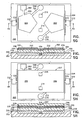
- Figures 1A , 1 Band 1 C show a plan view and two cross-sectional views, respectively, of a first embodiment 100 of a thin-film acoustically-coupled transformer in accordance with the invention.
- Transformer 100 has a 1:1 impedance transformation ratio, is capable of linking single-ended circuitry with balanced circuitry or vice versa and provides electrical isolation between primary and secondary.
- Transformer 100 is composed of a stacked bulk acoustic resonator (SBAR) 106, first terminals 132 and 134 and second terminals 136 and 138.
- SBAR 106 is composed of a stacked pair of film bulk acoustic resonators (FBARs) 110 and 120 and an acoustic decoupler 130 between them.
- FBAR 120 is stacked atop FBAR 110.
- FBAR 110 is composed of opposed planar electrodes 112 and 114 and a layer of piezoelectric material 116 between the electrodes.
- FBAR 120 is composed of opposed planar electrodes 122 and 124 and a layer of piezoelectric material 126 between the electrodes.
- Acoustic decoupler 130 is located between electrode 114 of FBAR 110 and electrode 122 of FBAR 120. The acoustic decoupler controls the coupling of acoustic energy between FBARs 110 and 120.
- first terminals 132 and 134 are structured as bonding pads electrically connected by electrical traces 133 and 135, respectively, to electrodes 112 and 114, respectively, of FBAR 110.
- second terminals 136 and 138 are structured as bonding pads electrically connected by electrical traces 137 and 139, respectively, to electrodes 122 and 124, respectively, of FBAR 120.
- first terminals 132 and 134 constitute the primary terminals and the second terminals 136 and 138 constitute the secondary terminals of thin-film acoustically-coupled transformer 100.
- first terminals 132 and 134 constitute the secondary terminals and second terminals 136 and 138 constitute the primary terminals of thin-film acoustically-coupled transformer 100.
- SBAR 106 is suspended over a cavity 104 defined in a substrate 102. Suspending the SBAR over a cavity allows the FBARs of the SBAR to resonate mechanically. Other suspension schemes that allow the FBARs to resonate mechanically are possible.
- the SBAR can be located over a mismatched acoustic Bragg reflector (not shown) formed in or on substrate 102, as disclosed by Lakin in United States patent no. 6,107,721 , the disclosure of which is incorporated into this disclosure by reference.
- Ruby's disclosure also discloses a stacked film bulk acoustic resonator (SBAR) composed of two layers of piezoelectric material interleaved with three planar electrodes.
- Ruby's SBAR can be regarded as being composed of a stacked pair of FBARs in which one electrode is common to both FBARs, and will be referred to as a common-electrode SBAR.
- the common electrode renders the common-electrode SBAR incapable of linking balanced to unbalanced circuits and vice versa and of providing electrical isolation between primary and secondary. Moreover, the common electrode SBAR exhibits an extremely narrow pass bandwidth that makes it unsuitable for use in most applications. The narrow pass bandwidth is the result of the common electrode, which over couples acoustic energy between the FBARs.
- acoustic decoupler 130 controls the coupling of acoustic energy between stacked FBARs 110 and 120 and additionally electrically isolates FBAR 110 from FBAR 120.
- the electrical isolation provided by acoustic decoupler 130 enables transformer 100 to link balanced to unbalanced circuits and vice versa and provides electrical isolation between primary and secondary.
- the acoustic coupling provided by acoustic decoupler 130 is substantially less than the acoustic coupling between the FBARs in the common electrode SBAR referred to above.
- FBARs 110 and 120 are not over coupled, and transformer 100 has a relatively flat response in the pass band, as will be described below with reference to Figure 2 .
- the embodiment of the acoustic decoupler 130 shown in Figures 1A-1C is a first embodiment composed of layer 131 of acoustic decoupling material located between the electrodes 114 and 122 of FBARs 110 and 120, respectively.
- Figure 1D is an enlarged view showing this first embodiment of the acoustic decoupler in more detail.
- Important properties of the acoustic decoupling material of layer 131 that constitutes acoustic decoupler 130 are an acoustic impedance less than that of the materials of FBARs 110, 120, a high electrical resistivity, a low dielectric permittivity and a nominal thickness that is an odd integral multiple of one quarter of the wavelength in the acoustic decoupling material of an acoustic wave having a frequency equal to the center frequency of the pass band of acoustically-coupled transformer 100.
- the acoustic decoupling material of acoustic decoupler 130 has an acoustic impedance less that of the materials of FBARs 110 and 120 and substantially greater than that of air.
- the acoustic impedance of a material is the ratio of stress to particle velocity in the material and is measured in Rayleighs, abbreviated as rayl .
- the materials of the FBARs are typically aluminum nitride (AlN) as the material of piezoelectric layers 116, 126 and molybdenum (Mo) as the material of electrodes 112, 114, 122 and 124.
- the acoustic impedances of the materials of the FBARs are typically greater than 30 Mrayl (35 Mrayl for AIN and 63 Mrayl for Mo) and the acoustic impedance of air is about 1 krayl.
- materials with an acoustic impedance in the range from about 2 Mrayl to about 16 Mrayl work well as the acoustic coupling material of acoustic decoupler 130.
- Figure 2 is a graph showing how the calculated frequency response of thin-film acoustically-coupled transformer 100 depends on the acoustic impedance of the acoustic decoupling material of layer 131 that constitutes the first embodiment of acoustic decoupler 130.
- the embodiment illustrated has a center frequency of about 1,900 MHz.
- Calculated frequency responses for embodiments in which the acoustic decoupling material of the acoustic decoupler has acoustic impedances of about 4 Mrayl (polyimide ⁇ curve 140), 8 Mrayl (curve 142) and 16 Mrayl (curve 144) are shown.
- the bandwidth of transformer 100 increases with increasing acoustic impedance of the acoustic decoupling material.
- the acoustic impedance is 16 Mrayl
- the resonances of the FBARs are over coupled, which causes the characteristic double peak in the pass band response.
- acoustic decoupler 130 shown in Figures 1B, 1C and 1D is composed of layer 131 of acoustic decoupling material with a nominal thickness equal to one quarter of the wavelength in the acoustic decoupling material of an acoustic wave having a frequency equal to the center frequency of the transformer's pass band, i.e., t ⁇ ⁇ n /4, where t is the thickness of the layer 131 of acoustic decoupling material that constitutes acoustic decoupler 130 and ⁇ n is the wavelength in the acoustic decoupling material of an acoustic wave having a frequency equal to the center frequency of the pass band of transformer 100.
- a thickness of layer 131 within approximately ⁇ 10% of the nominal thickness can alternatively be used. A thickness outside this range can alternatively be used with some degradation in performance. However, the thickness of layer 131 should differ significantly from 0 ⁇ n at one extreme and ⁇ n /2 at the other extreme.
- the first embodiment of acoustic decoupler 130 shown in Figure 1D is composed of layer 131 of acoustic decoupling material with a nominal thickness equal to an odd integral multiple of one quarter of the wavelength in the acoustic decoupling material of an acoustic wave having a frequency equal to the center frequency of the pass band of transformer 100, i.e., t ⁇ (2 m + 1) ⁇ n /4, where t and ⁇ n are as defined above and m is an integer equal to or greater than zero.
- a thickness of layer 131 that differs from the nominal thickness by approximately ⁇ 10% of ⁇ n /4 can alternatively be used.
- a thickness tolerance outside this range can be used with some degradation in performance, but the thickness of layer 131 should differ significantly from an integral multiple of ⁇ n /2.
- plastic materials have acoustic impedances in the range stated above and can be applied in layers of uniform thickness in the thickness ranges stated above. Such plastic materials are therefore potentially suitable for use as the acoustic decoupling material of layer 131 of acoustic decoupler 130.
- the acoustic decoupling material must also be capable of withstanding the temperatures of the fabrication operations performed after layer 131 of acoustic decoupling material has been deposited on electrode 114 to form acoustic decoupler 130.
- electrodes 122 and 124 and piezoelectric layer 126 are deposited by sputtering after layer 131 has been deposited. Temperatures as high as 300 °C are reached during these deposition processes. Thus, a plastic that remains stable at such temperatures is used as the acoustic decoupling material.
- Plastic materials typically have a very high acoustical attenuation per unit length compared with the other materials of FBARs 110 and 120.
- acoustic decoupler 130 is composed of layer 131 of plastic acoustic decoupling material typically less than 1 ⁇ m thick, the acoustic attenuation introduced by layer 131 is typically negligible.
- a polyimide is used as the acoustic decoupling material of layer 131.
- Polyimide is sold under the trademark Kapton® by E.I. du Pont de Nemours and Company.
- acoustic decoupler 130 is composed of layer 131 of polyimide applied to electrode 114 by spin coating.
- Polyimide has an acoustic impedance of about 4 Mrayl.
- a poly(para-xylylene) is used as the acoustic decoupling material of layer 131.
- acoustic decoupler 130 is composed of layer 131 of poly(para-xylylene) applied to electrode 114 by vacuum deposition.
- Poly(para-xylylene) is also known in the art as parylene.
- the dimer precursor di-para-xylylene from which parylene is made and equipment for performing vacuum deposition of layers of parylene are available from many suppliers.
- Parylene has an acoustic impedance of about 2.8 Mrayl.
- the acoustic decoupling material of layer 131 constituting acoustic decoupler 130 has an acoustic impedance substantially greater than the materials of FBARs 110 and 120. No materials having this property are known at this time, but such materials may become available in future, or lower acoustic impedance FBAR materials may become available in future.
- the thickness of layer 131 of such high acoustic impedance acoustic decoupling material is as described above.
- FIG. 1E is an enlarged view of part of thin-film acoustically-coupled transformer 100 showing a second embodiment of acoustic decoupler 130 that incorporates a Bragg structure 161.
- Bragg structure 161 is composed of a low acoustic impedance Bragg element 163 sandwiched between high acoustic impedance Bragg elements 165 and 167.
- Low acoustic impedance Bragg element 163 is a layer of a low acoustic impedance material whereas high acoustic impedance Bragg elements 165 and 167 are each a layer of high acoustic impedance material.
- the acoustic impedances of the Bragg elements are characterized as "low” and “high” with respect to one another and additionally with respect to the acoustic impedance of the piezoelectric material of layers 116 and 126. At least one of the Bragg elements additionally has a high electrical resistivity and a low dielectric permittivity to provide electrical isolation between input and output of transformer 100.
- Each of the layers constituting Bragg elements 161, 163 and 165 has a nominal thickness equal to an odd integral multiple of one quarter of the wavelength in the material the layer of an acoustic wave having a frequency equal to the center frequency of transformer 100. Layers that differ from the nominal thickness by approximately ⁇ 10% of one quarter of the wavelength can alternatively be used. A thickness tolerance outside this range can be used with some degradation in performance, but the thickness of the layers should differ significantly from an integral multiple of one-half of the wavelength.
- low acoustic impedance Bragg element 163 is a layer of silicon dioxide (SiO 2 ), which has an acoustic impedance of about 13 Mrayl
- each of the high acoustic impedance Bragg elements 165 and 167 is a layer of the same material as electrodes 114 and 122, respectively, i.e., molybdenum, which has an acoustic impedance of about 63 Mrayl.
- high acoustic impedance Bragg elements 165 and 167 and electrodes 114 and 122, respectively, of FBARs 110 and 120, respectively allows high acoustic impedance Bragg elements 165 and 167 additionally to serve as electrodes 114 and 122, respectively.
- high acoustic impedance Bragg elements 165 and 167 have a nominal thickness equal to one quarter of the wavelength in molybdenum of an acoustic wave having a frequency equal to the center frequency of the pass band of transformer 100, and low acoustic impedance Bragg element 163 had a nominal thickness equal to three quarters of the wavelength in SiO 2 of an acoustic wave having a frequency equal to the center frequency of the pass band of the transformer.
- Using a three-quarter wavelength-thick layer of SiO 2 instead of a one-quarter wavelength thick layer of SiO 2 as low acoustic impedance Bragg element 163 reduces the capacitance between FBARs 110 and 120.
- Bragg structure 161 may be composed of more than one (e.g., n ) low acoustic impedance Bragg element interleaved with a corresponding number (i.e., n + 1) of high acoustic impedance Bragg elements. Only one of the Bragg elements need be insulating.
- the Bragg structure may be composed of two low acoustic impedance Bragg element interleaved with three high acoustic impedance Bragg elements.
- Wafer-scale fabrication is used to fabricate thin-film acoustically-coupled transformers similar to thin-film acoustically-coupled transformer 100 thousands at a time. Wafer-scale fabrication makes each thin-film acoustically-coupled transformer inexpensive to fabricate. Thin-film acoustically-coupled transformer 100 can be made using a fabrication method similar to that to be described below with reference to Figures 5A-5T . Accordingly, a method of fabricating thin-film acoustically-coupled transformer 100 will not be separately described.
- first terminals 132 and 134 electrically connected to electrodes 112 and 114, respectively, as shown in Figures 1A and 1B and electrical connections are additionally made to second terminals 136 and 138 electrically connected to electrodes 122 and 124, respectively, as shown in Figures 1A and 1C .
- the electrical connections to first terminals 132 and 134 provide electrical connections to the primary of thin-film acoustically-coupled transformer 100 and the electrical connections to second terminals 136 and 138 provide electrical connections to the secondary of thin-film acoustically-coupled transformer 100.
- the electrical connections to second terminals 136 and 138 provide electrical connections to the primary of thin-film acoustically-coupled transformer 100 and the electrical connections to first terminals 132 and 134 provide electrical connections to the secondary of thin-film acoustically-coupled transformer 100.
- an input electrical signal applied to first terminals 132 and 134 which constitute the primary terminals of thin-film acoustically-coupled transformer 100, establishes a voltage difference between electrodes 112 and 114 of FBAR 110.
- the voltage difference between electrodes 112 and 114 mechanically deforms FBAR 110 at the frequency of the input electrical signal.
- acoustic decoupler 130 couples all or part of the acoustic energy resulting from the mechanical deformation of FBAR 110 to FBAR 120.
- the acoustic energy received from FBAR 110 mechanically deforms FBAR 120 at the frequency of the input electrical signal.
- FBAR 120 The mechanical deformation of FBAR 120 generates a voltage difference between electrodes 122 and 124 at the frequency of the input electrical signal.
- the voltage difference is output at second terminals 136 and 138, which constitute the secondary terminals of transformer 100, as an output electrical signal.
- Piezoelectricity is a linear effect, so the amplitude and phase of the input electrical signal applied to the first terminals is preserved in the output electrical signal output at the second terminals.
- An embodiment of thin-film acoustically-coupled transformer 100 in which second terminals 136 and 138 constitute the primary terminals and first terminals 132 and 134 constitute the secondary terminals operates similarly, except acoustic energy propagates through acoustic decoupler 130 from FBAR 120 to FBAR 110.
- thin-film acoustically-coupled transformer 100 provides a 1:1 impedance transformation ratio, is capable of linking single-ended circuitry with balanced circuitry or vice versa and provides electrical isolation between primary and secondary.
- the capacitance between electrode 112 and substrate 102 differs from that between electrode 114 and the substrate.
- thin-film acoustically-coupled transformer 100 is not perfectly balanced electrically and can have an insufficient common-mode rejection ratio (CMRR) for certain applications.
- CMRR common-mode rejection ratio
- FIGS 3A-3C show a plan view and two cross-sectional views, respectively, of a second embodiment 200 of a thin-film acoustically-coupled transformer in accordance with the invention.
- Acoustically-coupled transformer 200 is capable of linking single-ended circuitry with balanced circuitry or vice versa, provides electrical isolation between primary and secondary. Some embodiments of transformer 200 are electrically balanced, and therefore have a high common-mode rejection ratio: other embodiments are electrically unbalanced and have a lower common-mode rejection ratio. Acoustically-coupled transformer 200 has an impedance transformation ratio of 1:1, 1:4 or 4:1 depending on the configurations of the electrical circuits that form part of the transformer.
- Acoustically-coupled transformer 200 is composed of two stacked bulk acoustic resonators (SBARs) 206 and 208. Each SBAR is composed of a stacked pair of film bulk acoustic resonators (FBARs) and an acoustic decoupler between the FBARs. Transformer 200 is additionally composed of an electrical circuit that connects one of the FBARs of SBAR 206 to one of the FBARs of SBAR 208, and an electrical circuit that connects the other of the FBARs of SBAR 206 to the other of the FBARs of SBAR 208.
- SBARs bulk acoustic resonators
- SBAR 206 is composed of a stacked pair of FBARs 210 and 220 and an acoustic decoupler 230 between them.
- SBAR 208 is composed of a stacked pair of FBARs 250 and 260 and an acoustic decoupler 270 between them.
- FBAR 220 is stacked atop FBAR 210 and FBAR 260 is stacked atop FBAR 250.
- FBAR 210 is composed of opposed planar electrodes 212 and 214 and a layer of piezoelectric material 216 between the electrodes.
- FBAR 220 is composed of opposed planar electrodes 222 and 224 and a layer of piezoelectric material 226 between the electrodes.
- FBAR 250 is composed of opposed planar electrodes 252 and 254 and a layer of piezoelectric material 256 between the electrodes.
- FBAR 260 is composed of opposed planar electrodes 262 and 264 and a layer of piezoelectric material 266 between the electrodes.
- an electrical circuit connects one of the FBARs of SBAR 206 to one of the FBARs of SBAR 208, and an electrical circuit connects the other of the FBARs of SBAR 206 to the other of the FBARs of SBAR 206.
- Each electrical circuit electrically connects the respective FBARs in any one of a parallel, a series, an anti-parallel and an anti-series configuration. Of the sixteen possible combinations of the parallel, series, anti-parallel and anti-series electrical circuit configurations, only eight produce a working transformer.
- the combination of electrical circuit configurations connecting the FBARs determines whether the transformer is electrically balanced (high common-mode rejection ratio) or electrically unbalanced, and determines the impedance transformation ratio of the transformer, i.e., 1:1, 1:4 or 4:1.
- Table 1 Parallel Series Anti-par. Anti-series Parallel U 1:1 X X U 1:4 Series X B 1:1 B 4:1 X Anti-par. X B 1:4 B 1:1 X Anti-series U 4:1 X X U 1:1
- the row captions indicate the configuration of one of the electrical circuits, e.g., electrical circuit 245 described below with reference to Figure 4C
- the column captions indicate the configuration of the other of the electrical circuits, e.g., electrical circuit 246 described with reference to Figure 4C
- B denotes that the transformer is electrically balanced
- U denotes that the transformer is unbalanced
- X denotes a non-functioning transformer.
- the impedance transformation ratio shown is the impedance transformation from electrical terminals connected to the electrical circuit indicated by the row caption to electrical terminals connected to the electrical circuit indicated by the column caption.
- the electrical circuits shown in Table 1 are subject to the constraint that an electrical circuit may only connect the electrodes of FBARs at the same level as one another in SBARs 206 and 208, i.e., one of the electrical circuits may only connect the electrodes of FBARs 210 and 250 and the other of the electrical circuits may only connect the electrodes of FBARs 220 and 260.
- Table 1 additionally assumes that the c-axes of piezoelectric layers 216, 226, 256 and 266 are all oriented in the same direction.
- More electrical circuits are possible in embodiments not subject to the constraint, e.g., in embodiments in which an electrical circuit is allowed to connect the electrodes of FBARs 210 and 260 and the electrodes of FBARs 220 and 250, and/or the assumption.
- An FBAR is a polarity-dependent device. A voltage of a given polarity applied between the electrodes of the FBAR will cause the FBAR to contract mechanically while the same voltage of the opposite polarity will cause the FBAR to expand mechanically by the same amount.
- a mechanical stress applied to the FBAR that causes the FBAR to contract mechanically will generate a voltage of the given polarity between the electrodes of the FBAR whereas a mechanical stress that causes the FBAR to expand mechanically will generate a voltage of the opposite polarity between the electrodes of the FBAR.
- the electrodes of the FBARs that an electrical circuit connects in parallel are at the same level in the respective SBARs.
- a signal applied to the FBARs connected in parallel produces signals of the same phase across the FBARs.
- the FBARs therefore expand and contract in phase, and generate acoustic energy in phase.
- electrodes of the FBARs that an electrical circuit connects in anti-parallel are at different levels in the respective SBARs.
- a signal applied to FBARs connected in anti-parallel produces signals of the opposite phases across the FBARs. The FBARs therefore expand and contract in antiphase, and generate acoustic energy in antiphase.
- the electrodes of the FBARs that an electrical circuit connects in series are at the same level in the respective SBARs.
- a signal applied to the FBARs connected in series produces signals of opposite phases across the FBARs.
- the FBARs expand and contract in antiphase, and generate acoustic energy in antiphase.
- the electrodes of the FBARs that an electrical circuit connects in anti-series are at different levels in the respective SBARs.
- a signal applied to the FBARs connected in anti-series produces signals of the same phase across the FBARs.
- the FBARs expand and contract in phase and generate acoustic energy in phase.
- FBARs receiving acoustic energy that causes them to expand and contract in phase generate signals in phase.
- Connecting FBARs that generate signals in phase in parallel produces a signal level equal to that across the individual FBARs and an impedance of one-half the characteristic impedance of the individual FBARs.
- Connecting such FBARs in anti-series produces a signal level of twice that across the individual FBARs and an impedance of twice the characteristic impedance of the individual FBARs.
- connecting FBARs that generate signals in phase in anti-parallel or in series causes the signals to cancel.
- FBARs receiving acoustic energy that causes them to expand and contract in antiphase generate signals in antiphase.
- Connecting FBARs that generate signals in antiphase in antiparallel produces a signal equal in level to that across the individual FBARs and an impedance of one-half the characteristic impedance of the individual FBARs. Connecting such FBARs in series produces a signal of twice the level of that across the individual FBARs and an impedance of twice the characteristic impedance of the individual FBARs. However, connecting FBARs that generate signals in antiphase in parallel or in antiseries causes the signals to cancel.
- the transformers indicated in Table 1 as being non-functional are transformers in which the FBARs that receive acoustic energy generate signals that cancel.
- Figures 4A and 4B schematically illustrate two configurations of electrical circuits that connect the FBARs 210 and 220 of SBAR 206 and the FBARs 250 and 260 of SBAR 208 in anti-parallel or in series, respectively, to form respective electrically-balanced embodiments of an acoustically-coupled transformer having a 1:1 impedance transformation ratio.
- Figure 4A shows an electrical circuit 241 electrically connecting one of the FBARs of SBAR 206 in anti-parallel with one of the FBARs of SBAR 208 and to first terminals F and an electrical circuit 242 electrically connecting the other of the FBARs of SBAR 206 in anti-parallel with the other of the FBARs of SBAR 208 and to second terminals S.
- the electrical circuit 241 electrically connects FBAR 220 of SBAR 206 in anti-parallel with FBAR 260 of SBAR 208 and to first terminals F
- electrical circuit 242 electrically connects FBAR 210 of SBAR 206 in anti-parallel with FBAR 250 of SBAR 208 and to second terminals S.
- electrical circuit 241 electrically connects electrode 222 of FBAR 220 to electrode 264 of FBAR 260 and to one of the first terminals F and additionally electrically connects electrode 224 of FBAR 220 to electrode 262 of FBAR 260 and to the other of the first terminals F.
- Electrical circuit 242 electrically connects electrode 214 of FBAR 210 to electrode 252 of FBAR 250 and to one of the second terminals S and additionally electrically connects electrode 212 of FBAR 210 to electrode 254 of FBAR 250 and to the other of the second terminals S.
- Electrical circuit 241 electrically connects FBARs 220 and 260 in anti-parallel so that an input electrical signal applied to the first terminals F is applied equally but in antiphase to FBARs 220 and 260. Electrical circuit 241 electrically connects FBARs 220 and 260 in anti-parallel in the sense that an electrical signal applied to first terminals F that causes FBAR 220 to contract mechanically additionally causes FBAR 260 to expand mechanically by the same amount, and vice versa. The acoustic energy generated by FBAR 260 is therefore in antiphase with the acoustic energy generated by FBAR 220.
- the acoustic energy received by FBAR 250 from FBAR 260 is in antiphase with the acoustic energy received by FBAR 210 from FBAR 220, and the signal between electrodes 214 and 212 is in antiphase with the signal between electrodes 254 and 252.
- Electrical circuit 242 connects FBARs 210 and 250 in anti-parallel, so that the signal output to the second terminals S is in phase with the signal between electrodes 214 and 212 and also with the signal between electrodes 254 and 252. As a result, the signal between second terminals S is the same as the signal across either of FBARs 210 and 250.
- Each first terminal has connected to it one electrode closer to the substrate and one electrode further from the substrate.
- one first terminal has electrode 222 closer to the substrate and electrode 264 further from the substrate connected to it and the other first terminal has electrode 262 closer to the substrate and electrode 224 further from the substrate connected to it.
- substantially the same capacitance exists between each of the second terminals S and substrate 202.
- Each second terminal has connected to it one electrode closer to the substrate and one electrode further from the substrate.
- one second terminal has electrode 212 closer to the substrate and electrode 254 further from the substrate connected to it and the other second terminal has electrode 252 closer to the substrate and electrode 214 further from the substrate connected to it.
- the embodiment of thin-film acoustically-coupled transformer 200 shown in Figure 4A is electrically balanced and, as a result, has a common-mode rejection ratio sufficiently high for many more applications than the thin-film acoustically-coupled transformer 100 described above with reference to Figures 1A-1C .
- the embodiment of thin-film acoustically-coupled transformer 200 shown in Figure 4A has a 1:1 impedance transformation ratio.
- First terminals F may serve as the primary terminals or the secondary terminals of the transformer and second terminals P may serve as the secondary terminals or the primary terminals, respectively, of the transformer.
- An input electrical signal applied to the primary terminals is output at substantially the same level at the secondary terminals.
- the impedance seen at the primary terminals and at the secondary terminals is that of two FBARs in parallel, i.e., one half of the typical characteristic impedance of a single FBAR.
- the embodiment of thin-film acoustically-coupled transformer 200 shown in Figure 4A is suitable for use in relatively low characteristic impedance applications.
- Figure 4B schematically shows an electrical circuit 243 electrically connecting one of the FBARs of SBAR 206 and one of the FBARs of SBAR 208 in series between first terminals F and an electrical circuit 244 electrically connecting the other of the FBARs of SBAR 206 and the other of the FBARs of SBAR 208 in series between second terminals S.
- electrical circuit 243 electrically connects FBAR 220 of SBAR 206 and FBAR 260 of SBAR 208 in series between first terminals F
- electrical circuit 244 electrically connects FBAR 210 of SBAR 206 and FBAR 250 of SBAR 208 in series between second terminals S.
- electrical circuit 243 electrically connects electrode 222 of FBAR 220 to electrode 262 of FBAR 260 and additionally electrically connects electrode 224 of FBAR 220 to one of the first terminals F and electrically connects electrode 264 of FBAR 260 to the other of the first terminals F.
- electrical circuit 243 electrically connects electrode 224 of FBAR 220 to electrode 264 of FBAR 260 and additionally electrically connects electrode 222 of FBAR 220 and electrode 262 of FBAR 260 to first terminals F.
- Electrical circuit 244 electrically connects electrode 212 of FBAR 210 to electrode 252 of FBAR 250 and additionally electrically connects electrode 214 of FBAR 210 to one of the second terminals S and additionally electrically connects electrode 254 of FBAR 250 to the other of the second terminals S.
- electrical circuit 244 electrically connects electrode 214 of FBAR 210 to electrode 254 of FBAR 250 and additionally electrically connects electrode 212 of FBAR 210 and electrode 252 of FBAR 250 to second terminals S.
- Electrical circuit 243 electrically connecting FBARs 220 and 260 in series divides an input electrical signal applied to the first terminals F approximately equally between FBARs 220 and 260.
- FBARs 220 and 260 are connected in series in the sense that an electrical signal applied to first terminals F that causes FBAR 220 to contract mechanically causes FBAR 260 to expand mechanically by the same amount, and vice versa.
- the acoustic energy generated by FBAR 260 is therefore in antiphase with the acoustic energy generated by FBAR 220.
- the acoustic energy received by FBAR 250 from FBAR 260 is in antiphase with the acoustic energy received by FBAR 210 from FBAR 220 and the signal on electrode 254 is in antiphase with the signal on electrode 214.
- Electrical circuit 244 electrically connects FBARs 210 and 250 in series so that the signal at second terminals S is twice the signal across either of FBARs 210 and 250.
- Electrodes 224 and 264 connected to the first terminals are at the same distance from the substrate.
- substantially the same capacitance exists between each of the second terminals S and substrate 202.
- Electrodes 214 and 254 connected to the second terminals are at the same distance from the substrate.
- the embodiment of thin-film acoustically-coupled transformer 200 shown in Figure 4B is electrically balanced and, as a result, has a common-mode rejection ratio sufficiently high for many more applications than the thin-film acoustically-coupled transformer 100 described above with reference to Figures 1A-1C .
- the embodiment of thin-film acoustically-coupled transformer 200 shown in Figure 4B has a 1:1 impedance transformation ratio.
- First terminals F may serve as the primary terminals or the secondary terminals of the transformer and second terminals P may serve as the secondary terminals or the primary terminals, respectively, of the transformer.
- An input electrical signal applied to the primary terminals is output at substantially the same level at the secondary terminals.
- the impedance seen at the primary terminals and at the secondary terminals is that of two FBARs in series, i.e., twice the typical characteristic impedance of a single FBAR.
- the embodiment of thin-film acoustically-coupled transformer 200 shown in Figure 4B is suitable for use in higher characteristic impedance applications than that shown in Figure 4A .
- Figures 4C and 4D schematically illustrate two configurations of electrical circuits that connect the FBARs 210 and 220 of SBAR 206 and the FBARs 250 and 260 of SBAR 208 in anti-parallel and in series to form respective embodiments of an acoustically-coupled transformer having a 1:4 or 4:1 impedance transformation ratio.
- Figure 4C shows an electrical circuit 245 electrically connecting one of the FBARs of SBAR 206 in anti-parallel with one of the FBARs of SBAR 208 and to first terminals F and an electrical circuit 246 electrically connecting the other of the FBARs of SBAR 206 and the other of the FBARs of SBAR 208 in series between second terminals S.
- the electrical circuit 245 electrically connects FBAR 220 of SBAR 206 in anti-parallel with FBAR 260 of SBAR 208 and to first terminals P, and electrical circuit 246 electrically connects FBAR 210 of SBAR 206 and FBAR 250 of SBAR 208 in series between second terminals S.
- electrical circuit 245 electrically connects electrode 222 of FBAR 220 to electrode 264 of FBAR 260 and to one of the first terminals F, and additionally electrically connects electrode 224 of FBAR 220 to electrode 262 of FBAR 260 and to the other of the first terminals F.
- Electrical circuit 246 electrically connects electrode 214 of FBAR 210 to electrode 254 of FBAR 250 and additionally electrically connects electrode 212 of FBAR 210 to one of the second terminals S and electrode 252 of FBAR 250 to the other of the second terminals S.
- electrical circuit 246 electrically connects electrode 212 of FBAR 210 to electrode 252 of FBAR 250 and additionally electrically connects electrode 214 of FBAR 210 and electrode 254 of FBAR 250 to second terminals S.
- Electrical circuit 245 electrically connects FBARs 220 and 260 in anti-parallel so that an input electrical signal applied to the first terminals F is applied equally but in antiphase to FBARs 220 and 260. Electrical circuit 245 electrically connects FBARs 220 and 260 in anti-parallel in the sense that an electrical signal applied to first terminals F that causes FBAR 220 to contract mechanically additionally causes FBAR 260 to expand mechanically by the same amount, and vice versa. The acoustic energy generated by FBAR 260 is therefore in antiphase with the acoustic energy generated by FBAR 220.
- acoustic energy received by FBAR 250 from FBAR 260 is in antiphase with the acoustic energy received by FBAR 210 from FBAR 220, and the signal on electrode 252 is in antiphase with the signal on electrode 212.
- Electrical circuit 246 connects FBARs 210 and 250 in series so that the voltage difference between second terminals S is twice the voltage across either of FBARs 210 and 250.
- Each first terminal has connected to it one electrode closer to the substrate and one electrode further from the substrate.
- one first terminal has electrode 222 closer to the substrate and electrode 264 further from the substrate connected to it and the other first terminal has electrode 262 closer to the substrate and electrode 224 further from the substrate connected to it.
- substantially the same capacitance exists between each of the second terminals S and substrate 202. Electrodes 212 and 252 connected to the second terminals are at the same distance from the substrate.
- the embodiment of thin-film acoustically-coupled transformer 200 shown in Figure 4C is electrically balanced and, as a result, has a common-mode rejection ratio sufficiently high for many more applications than the thin-film acoustically-coupled transformer 100 described above with reference to Figures 1A-1C .
- thin-film acoustically-coupled transformer 200 shown in Figure 4C is a step-up transformer when first terminals F serve as primary terminals and second terminals S serve as secondary terminals. A signal applied to the primary terminals is output at twice the level at the secondary terminals.
- the impedance seen at the primary terminals is that of two FBARs in parallel, i.e., one half of the typical characteristic impedance of a single FBAR, whereas the impedance seen at the secondary terminals is that of two FBARs in series, i.e., twice the typical characteristic impedance of a single FBAR.
- the embodiment of thin-film acoustically-coupled transformer 200 illustrated in Figure 4C has a 1:4 primary-to-secondary impedance ratio.
- the embodiment of thin-film acoustically-coupled transformer 200 shown in Figure 4C is a step-down transformer when first terminals F serve as secondary terminals and second terminals S serve as primary terminals.
- the signal output at the secondary terminals is one-half the level of the input electrical signal applied to the primary terminals, and the primary-to-secondary impedance ratio is 4:1.
- Figure 4D schematically shows an electrical circuit 247 electrically connecting FBAR 220 of SBAR 206 and FBAR 260 of SBAR 208 in series between first terminals F, and an electrical circuit 248 electrically connecting FBAR 210 of SBAR 206 and FBAR 250 of SBAR 208 in anti-parallel and to second terminals S.
- electrical circuit 247 electrically connects electrode 222 of FBAR 220 to electrode 262 of FBAR 260 and additionally electrically connects electrode 224 of FBAR 220 and electrode 264 of FBAR 260 to first terminals F.
- Electrical circuit 248 electrically connects electrode 212 of FBAR 210 to electrode 254 of FBAR 250 and to one of the second terminals S, and additionally electrically connects electrode 214 of FBAR 210 to electrode 252 of FBAR 250 and to the other of the second terminals S.
- electrical circuit 247 electrically connects electrode 224 of FBAR 220 to electrode 264 of FBAR 260 and additionally electrically connects electrode 222 of FBAR 220 and electrode 262 of FBAR 260 to first terminals F.
- Electrical circuit 247 electrically connecting FBARs 220 and 260 in series divides an input electrical signal applied to the first terminals F approximately equally between FBARs 220 and 260.
- FBARs 220 and 260 are connected in series in the sense that an electrical signal applied to first terminals F that causes FBAR 220 to contract mechanically causes FBAR 260 to expand mechanically by the same amount, and vice versa.
- the acoustic energy generated by FBAR 260 is therefore in antiphase with the acoustic energy generated by FBAR 220.
- the acoustic energy received by FBAR 250 from FBAR 260 is in antiphase with the acoustic energy received by FBAR 210 from FBAR 220 and the voltage between electrodes 252 and 254 is in antiphase with the voltage between electrodes 212 and 214.
- Electrical circuit 248 electrically connects FBARs 210 and 250 in anti-parallel, so that the signal output at the second terminals S is in phase with the signal across electrodes 214 and 212 and also with the signal across electrodes 254 and 252.
- the signal at second terminals S is equal in level to the signal across either of FBARs 210 and 250, and is equal to one-half the level of the input electrical signal applied to first terminals F.
- the embodiment of thin-film acoustically-coupled transformer 200 shown in Figure 4D is electrically balanced and, as a result, has a common-mode rejection ratio sufficiently high for many more applications than the thin-film acoustically-coupled transformer 100 described above with reference to Figures 1A-1C .
- thin-film acoustically-coupled transformer 200 shown in Figure 4D is a step-down transformer when first terminals F serve as primary terminals and second terminals S serve as secondary terminals.
- the signal level output at the secondary terminals is one-half that of the input electrical signal applied to the primary terminals.
- the impedance seen at the primary terminals is that of two FBARs in series, i.e., twice the typical characteristic impedance of a single FBAR, whereas the impedance seen at the secondary terminals is that of two FBARs in parallel, i.e., one-half of the typical characteristic impedance of a single FBAR.
- the embodiment of thin-film acoustically-coupled transformer 200 illustrated in Figure 4D has a 4:1 primary-to-secondary impedance ratio.
- the embodiment of thin-film acoustically-coupled transformer 200 shown in Figure 4D is a step-up transformer when first terminals F serve as secondary terminals and second terminals S serve as primary terminals.
- the signal level output at the secondary terminals is twice that of the input electrical signal applied to the primary terminals, and the primary-to-secondary impedance ratio is 1:4.
- Figure 4E shows an embodiment of an acoustically-coupled transformer with a 1:1 impedance transformation ratio in which an electrical circuit 341 connects FBAR 220 of SBAR 206 and FBAR 260 of SBAR 208 in parallel and to first terminals F, and an electrical circuit 342 electrically connects FBAR 210 of SBAR 206 and FBAR 250 of SBAR 208 in parallel and to second terminals S.
- Figure 4F shows an embodiment of an acoustically-coupled transformer with a 1:1 impedance transformation ratio in which an electrical circuit 343 connects FBAR 220 of SBAR 206 and FBAR 260 of SBAR 208 in anti-series between first terminals F, and an electrical circuit 344 connects FBAR 210 of SBAR 206 and FBAR 250 of SBAR 208 in anti-series between second terminals S.
- Figure 4G shows an embodiment of an acoustically-coupled transformer in which an electrical circuit 345 electrically connects FBAR 220 of SBAR 206 and FBAR 260 of SBAR 208 in parallel and to first terminals F, and an electrical circuit 346 electrically connects FBAR 210 of SBAR 206 and FBAR 250 of SBAR 208 in anti-series between second terminals S.
- This embodiment has a 1:4 impedance transformation ratio when first terminals F serve as primary terminals and second terminals S serve as secondary terminals, or a 4:1 impedance transformation ratio when second terminals S serve as the primary terminals and first terminals F serve as the secondary terminals.
- Figure 4H shows an embodiment of an acoustically-coupled transformer in which electrical circuit 347 electrically connects FBAR 220 of SBAR 206 and FBAR 260 of SBAR 208 in anti-series between first terminals F, and an electrical circuit 348 electrically connects FBAR 210 of SBAR 206 and FBAR 250 of SBAR 208 in parallel and to second terminals S.
- This embodiment has a 4:1 impedance transformation ratio when first terminals F serve as primary terminals and second terminals S serve as secondary terminals, or a 1:4 impedance transformation ratio when second terminals S serve as the primary terminals and first terminals F serve as the secondary terminals.
- a bonding pad 282 and a bonding pad 284 constitute the first terminals of thin-film acoustically-coupled transformer 200.
- An interconnection pad 236, an electrical trace 237 extending from electrode 222 to interconnection pad 236 ( Figure 5G ), an interconnection pad 278 in electrical contact with interconnection pad 236 and an electrical trace 279 extending from electrode 264 to interconnection pad 278 constitute the part of electrical circuit 245 ( Figure 4C ) that electrically connects electrode 222 of FBAR 220 to electrode 264 of FBAR 260.
- An interconnection pad 238, an electrical trace 239 extending from electrode 224 to interconnection pad 238, an interconnection pad 276 in electrical contact with interconnection pad 238 and an electrical trace 277 extending from electrode 262 to interconnection pad 276 ( Figure 5G ) constitute the part of electrical circuit 245 ( Figure 4C ) that electrically connects electrode 224 of FBAR 220 to electrode 262 of FBAR 260.
- An electrical trace 283 that extends between electrode 222 and bonding pad 282 and an electrical trace 285 that extends between electrode 264 and bonding pad 284 ( Figure 5G ) constitute the part of electrical circuit 245 that connects FBARs 220 and 260 connected in anti-parallel to the first terminals provided by bonding pads 282 and 284.
- bonding pads 282 and 284 and traces 283 and 285 are omitted and interconnection pads 238 and 278 are configured as bonding pads and provide the first terminals of thin-film acoustically-coupled transformer 200.
- Bonding pad 232 and bonding pad 272 constitute the second terminals of thin-film acoustically-coupled transformer 200.
- An electrical trace 235 that extends between electrode 214 and electrode 254 ( Figure 5E ) constitutes the part of electrical circuit 246 ( Figure 4C ) that connects FBAR 210 and FBAR 250 in series.
- An electrical trace 233 that extends between electrode 212 and bonding pad 232 and an electrical trace 273 that extends between electrode 252 and bonding pad 272 ( Figure 5C ) constitutes the part of electrical circuit 246 that connects FBAR 210 and FBAR 250 to the second terminals provided by bonding pads 232 and 272.
- acoustic decoupler 230 is located between FBARs 210 and 220, specifically, between electrodes 214 and 222. Acoustic decoupler 230 controls the coupling of acoustic energy between FBARs 210 and 220. Additionally, acoustic decoupler 270 is located between FBARs 250 and 260, specifically, between electrodes 254 and 262. Acoustic decoupler 270 controls the coupling of acoustic energy between FBARs 250 and 260. Acoustic decoupler 230 couples less acoustic energy between the FBARs 210 and 220 than would be coupled if the FBARs were in direct contact with one another.
- Acoustic decoupler 270 couples less acoustic energy between the FBARs 250 and 260 than would be coupled if the FBARs were in direct contact with one another.
- the coupling of acoustic energy defined by acoustic decouplers 230 and 270 determines the pass bandwidth of thin-film acoustically-coupled transformer 200.
- acoustic decouplers 230 and 270 are respective parts of a layer 231 of acoustic decoupling material.
- Important properties of the acoustic decoupling material of layer 231 are an acoustic impedance less than that of FBARs 210, 220, 250 and 260, a nominal thickness that is an odd integral multiple of one quarter of the wavelength in the acoustic decoupling material of an acoustic wave having a frequency equal to the center frequency of the pass band of the transformer 200, and a high electrical resistivity and low dielectric permittivity to provide electrical isolation between the primary and secondary of the transformer.
- acoustic decouplers 230 and 270 each include a Bragg structure similar to Bragg structure 161 described above with reference to Figure 1E . Acoustic decouplers 230 and 270 may alternatively share a common Bragg structure in a manner similar to the way in which the embodiments of acoustic couplers 230 and 270 shown in Figures 3A-3C share a common layer 231.
- SBAR 206 and SBARs 208 are located adjacent one another suspended over a cavity 204 defined in a substrate 202. Suspending the SBARs over a cavity allows the stacked FBARs in each SBAR to resonate mechanically. Other suspension schemes that allow the stacked FBARs to resonate mechanically are possible.
- the SBARs can be located over a mismatched acoustic Bragg reflector (not shown) formed in or on substrate 202, as disclosed by the above-mentioned United States patent no. 6,107,721 of Lakin.
- a wafer of single-crystal silicon is provided.
- a portion of the wafer constitutes, for each transformer being fabricated, a substrate corresponding to the substrate 202 of transformer 200.
- Figures 5A-5J and Figures 5K-5T illustrate and the following description describes the fabrication of transformer 200 in and on a portion of the wafer. As transformer 200 is fabricated, the remaining transformers on the wafer are similarly fabricated.
- the portion of the wafer that constitutes substrate 202 of transformer 200 is selectively wet etched to form cavity 204, as shown in Figures 5A and 5K .
- a layer of fill material (not shown) is deposited on the surface of the wafer with a thickness sufficient to fill the cavities. The surface of the wafer is then planarized to leave the cavity filled with the fill material.
- Figures 5B and 5L show cavity 204 in substrate 202 filled with fill material 205.
- the fill material was phosphosilicate glass (PSG) and was deposited using conventional low-pressure chemical vapor deposition (LPCVD).
- the fill material may alternatively be deposited by sputtering, or by spin coating.
- Electrode 212 and electrode 252 typically have an irregular shape in a plane parallel to the major surface of the wafer. An irregular shape minimizes lateral modes in FBAR 210 and FBAR 250 ( Figure 3A ) of which the electrodes form part, as described in United States patent no. 6,215,375 of Larson III et al.. Electrode 212 and electrode 252 are located to expose part of the surface of fill material 205 so that the fill material can later be removed by etching, as will be described below.
- electrodes 212, 214, 222, 224, 252, 254, 262 and 264 are defined are patterned such that, in respective planes parallel to the major surface of the wafer, electrodes 212 and 214 of FBAR 210 have the same shape, size, orientation and position, electrodes 222 and 224 of FBAR 220 have the same shape, size, orientation and position, electrodes 252 and 254 of FBAR 250 have the same shape, size, orientation and position and electrodes 262 and 264 of FBAR 260 have the same shape, size, orientation and position.
- electrodes 214 and 222 additionally have the same shape, size, orientation and position and electrodes 254 and 262 additionally have the same shape, size, orientation and position.
- the metal deposited to form electrode 212, bonding pad 232, trace 233, electrode 252, bonding pad 272 and trace 273 was molybdenum.
- the molybdenum was deposited with a thickness of about 440 nm by sputtering, and was patterned by dry etching to define pentagonal electrodes each with an area of about 26,000 square ⁇ m.
- Other refractory metals such as tungsten, niobium and titanium may alternatively be used as the material of electrodes 212 and 252, bonding pads 232 and 272 and traces 233 and 273.
- the electrodes, bonding pads and traces may alternatively comprise layers of more than one material.
- a layer of piezoelectric material is deposited and is patterned to define a piezoelectric layer 217 that provides piezoelectric layer 216 of FBAR 210 and piezoelectric layer 256 of FBAR 250, as shown in Figures 5D and 5N .
- Piezoelectric layer 217 is patterned to expose part of the surface of fill material 205 and bonding pads 232 and 272.
- Piezoelectric layer 217 is additionally patterned to define windows 219 that provide access to additional parts of the surface of the fill material.
- the piezoelectric material deposited to form piezoelectric layer 217 was aluminum nitride and was deposited with a thickness of about 780 nm by sputtering.
- the piezoelectric material was patterned by wet etching in potassium hydroxide or by chlorine-based dry etching.
- Alternative materials for piezoelectric layer 217 include zinc oxide and lead zirconium titanate.
- a layer of metal is deposited and is patterned to define electrode 214, electrode 254 and electrical trace 235 extending between electrode 214 and electrode 254, as shown in Figures 5E and 5O .
- the metal deposited to form electrode 214, electrode 254 and trace 235 was molybdenum.
- the molybdenum was deposited with a thickness of about 440 nm by sputtering, and was patterned by dry etching.
- Other refractory metals may alternatively be used as the material of electrodes 214 and 254 and trace 235.
- the electrodes and trace may alternatively comprise layers of more than one material.
- a layer of acoustic decoupling material is then deposited and is patterned to define an acoustic decoupling layer 231 that provides acoustic decoupler 230 and acoustic decoupler 270, as shown in Figures 5F and 5P .
- Acoustic decoupling layer 231 is shaped to cover at least electrode 214 and electrode 254, and is additionally shaped to expose part of the surface of fill material 205 and bonding pads 232 and 272. Acoustic decoupling layer 231 is additionally patterned to define windows 219 that provide access to additional parts of the surface of the fill material.
- the acoustic decoupling material was polyimide with a thickness of about 750 nm, i.e., three quarters of the center frequency wavelength in the polyimide.
- the polyimide was deposited to form acoustic decoupling layer 231 by spin coating, and was patterned by photolithography. Polyimide is photosensitive so that no photoresist is needed. As noted above, other plastic materials can be used as the acoustic decoupling material.
- the acoustic decoupling material can be deposited by methods other than spin coating.
- the wafer was baked at about 300 °C before further processing was performed.
- the bake evaporates volatile constituents of the polyimide and prevents the evaporation of such volatile constituents during subsequent processing from causing separation of subsequently-deposited layers.
- a layer of metal is deposited and is patterned to define electrode 222, interconnection pad 236, electrical trace 237 extending from electrode 222 to interconnection pad 236, bonding pad 282 and electrical trace 283 extending from electrode 222 to bonding pad 282, as shown in Figures 5G and 5Q .
- the patterning also defines in the layer of metal electrode 262, interconnection pad 276 and electrical trace 277 extending from electrode 262 to interconnection pad 276, also as shown in Figures 5G and 5Q .
- the metal deposited to form electrodes 222 and 262, bonding pad 282, interconnection pads 236 and 276 and electrical traces 237, 277 and 283 was molybdenum.
- the molybdenum was deposited with a thickness of about 440 nm by sputtering, and was patterned by dry etching.
- Other refractory metals may alternatively be used as the material of electrodes 222 and 262, pads 236, 276 and 282 and electrical traces 237, 277 and 283.
- the electrodes, bonding pads and traces may alternatively comprise layers of more than one material.
- a layer of piezoelectric material is deposited and is patterned to define piezoelectric layer 227 that provides piezoelectric layer 226 of FBAR 220 and piezoelectric layer 266 of FBAR 260.
- Piezoelectric layer 227 is shaped to expose pads 232, 236, 272, 276 and 282 and to expose part of the surface of fill material 205 as shown in Figures 5H and 5R .
- Piezoelectric layer 227 is additionally patterned to define the windows 219 that provide access to additional parts of the surface of the fill material.
- the piezoelectric material deposited to form piezoelectric layer 227 was aluminum nitride and was deposited with a thickness of about 780 nm by sputtering.
- the piezoelectric material was patterned by wet etching in potassium hydroxide or by chlorine-based dry etching.
- Alternative materials for piezoelectric layer 227 include zinc oxide and lead zirconium titanate.
- a layer of metal is deposited and is patterned to define electrode 224, interconnection pad 238 and electrical trace 239 extending from electrode 224 to interconnection pad 238, as shown in Figures 5I and 5S .
- Interconnection pad 238 is located in electrical contact with interconnection pad 276 to provide the part of electrical circuit 245 ( Figure 4C ) that connects electrodes 224 and 262.
- the patterning also defines in the layer of metal electrode 264, interconnection pad 278, electrical trace 279 extending from electrode 264 to interconnection pad 278, bonding pad 284 and electrical trace 285 extending from electrode 264 to bonding pad 284, also as shown in Figures 5I and 5S .
- Interconnection pad 278 is located in electrical contact with interconnection pad 236 to provide the part of electrical circuit 245 ( Figure 4C ) that connects electrodes 222 and 264.
- bonding pads 282 and 284 and electrical traces 283 and 285 may be omitted if reliable electrical connections can be made to stacked interconnection pads 236 and 278 and to stacked interconnection pads 276 and 238.
- the metal deposited to form electrodes 224 and 264, pads 238, 278 and 284 and electrical traces 237, 279 and 285 was molybdenum.
- the molybdenum was deposited with a thickness of about 440 nm by sputtering, and was patterned by dry etching.
- Other refractory metals such may alternatively be used as the material of electrodes 224 and 264, pads 238, 278 and 284 and electrical traces 237, 279 and 285.
- the electrodes, pads and traces may alternatively comprise layers of more than one material.
- the wafer is then isotropically wet etched to remove fill material 205 from cavity 204. As noted above, portions of the surface of fill material 205 remain exposed through, for example, windows 219. The etch process leaves thin-film acoustically-coupled transformer 200 suspended over cavity 204, as shown in Figures 5J and 5T .
- the etchant used to remove fill material 205 was dilute hydrofluoric acid.
- a gold protective layer is deposited on the exposed surfaces of pads 232, 238, 272, 278, 282 and 284.
- the wafer is then divided into individual transformers, including transformer 200. Each transformer is then mounted in a package and electrical connections are made between bonding pads 232, 272, 282 and 284 of the transformer and pads that are part of the package.
- a process similar to that described may be used to fabricate embodiments of thin-film acoustically-coupled transformer 200 in which the FBARs are electrically connected as shown in Figures 4B-4H .
- bonding pad 282 electrically connected to electrodes 222 and 264 and bonding pad 284 electrically connected to electrodes 224 and 262 provide the first terminals of the transformer 200
- bonding pad 232 electrically connected to electrode 212 and bonding pad 272 electrically connected to electrode 252 provide the second terminals of transformer 200.
- the first terminals provide the primary terminals and the second terminals provide the secondary terminals of thin-film acoustically-coupled transformer 200.
- the first terminals provide the secondary terminals and the second terminals provide the primary terminals of thin-film acoustically-coupled transformer 200.
- a layer of metal is deposited and is patterned to define a high acoustic impedance Bragg element incorporating electrodes 214 and 254 and additionally to define electrical trace 235 extending between the electrodes, in a manner similar to that shown in Figures 5E and 5O .
- the high acoustic impedance Bragg element is similar to high acoustic impedance Bragg element 165 shown in Figure 1E .
- the layer of metal is deposited with a nominal thickness equal to an odd, integral multiple of one quarter of the wavelength in the metal of an acoustic wave having a frequency equal to the center frequency of the pass band of transformer 200.
- the metal deposited to form the high acoustic impedance Bragg element incorporating electrodes 214 and 254 is molybdenum.
- the molybdenum is deposited with a thickness of about 820 nm (one-quarter wavelength in Mo) by sputtering, and is patterned by dry etching.
- Other refractory metals may alternatively be used as the material of the high acoustic impedance Bragg element incorporating electrodes 214 and 254.
- the high acoustic impedance Bragg element may alternatively comprise layers of more than one metal.
- a layer of low acoustic impedance material is then deposited and is patterned to define a low acoustic impedance Bragg element in a manner similar to that shown in Figures 5F and 5P .
- the layer of low acoustic impedance material is deposited with a nominal thickness equal to an odd, integral multiple of one quarter of the wavelength in the low acoustic impedance material of an acoustic wave having a frequency equal to the center frequency of the pass band of transformer 200.
- the low acoustic impedance Bragg element is shaped to cover at least the high acoustic impedance Bragg element, and is additionally shaped to expose part of the surface of fill material 205 and bonding pads 232 and 272.
- the layer of low acoustic impedance material is additionally patterned to define windows that provide access to additional parts of the surface of the fill material.
- the low acoustic impedance material is SiO 2 with a thickness of about 790 nm.
- the SiO 2 is deposited by sputtering, and is patterned by etching.
- Other low acoustic impedance material that can be used as the material of low acoustic impedance Bragg element include phosphosilicate glass (PSG), titanium dioxide and magnesium fluoride.
- PSG phosphosilicate glass
- titanium dioxide titanium dioxide
- magnesium fluoride magnesium fluoride
- a layer of metal is deposited and is patterned to define a high acoustic impedance Bragg element incorporating electrodes 222 and 262.
- the layer of metal is additionally patterned to define an interconnection pad 236, an electrical trace 237 extending from electrode 222 to interconnection pad 236, a bonding pad 282, an electrical trace 283 extending from electrode 222 to bonding pad 282, an interconnection pad 276 and an electrical trace 277 extending from electrode 262 to interconnection pad 276 in a manner similar to that shown in Figures 7G and 7Q.
- the layer of metal is deposited with a nominal thickness equal to an odd, integral multiple of one quarter of the wavelength in the metal of an acoustic wave having a frequency equal to the center frequency of the pass band of transformer 200.
- the metal deposited to form a high acoustic impedance Bragg element incorporating electrodes 222 and 262 is molybdenum.
- the molybdenum is deposited with a thickness of about 820 nm (one-quarter wavelength in Mo) by sputtering, and is patterned by dry etching.
- Other refractory metals may alternatively be used as the material of the high acoustic impedance Bragg element incorporating electrodes 222 and 262 and its associated pads and electrical traces.
- the high acoustic impedance Bragg element, pads and electrical traces may alternatively comprise layers of more than one material.
- a layer of piezoelectric material is then deposited and is patterned to define piezoelectric layer 227, as described above, and the process continues as described above to complete fabrication of transformer 200.
Description
- The present invention relates to an acoustically-coupled transformer. Bulk acoustic wave resonators and filters and, more particularly, bulk acoustic wave baluns used in filters and duplexers are described in
US2003/01288081 A1 - Transformers are used in many types of electronic device to perform such functions as transforming impedances, linking single-ended circuitry with balanced circuitry or vice versa and providing electrical isolation. However, not all transformers have all of these properties. For example, an auto-transformer does not provide electrical isolation.
- Transformers operating at audio and radio frequencies up to VHF are commonly built as coupled primary and secondary windings around a high permeability core. The core contains the magnetic flux and increases the coupling between the windings. A transformer operable in this frequency range can also be realized using an optical-coupler. An opto-coupler used in this mode is referred to in the art as an opto-isolator.
- In transformers based on coupled windings or opto-couplers, the input electrical signal is converted to a different form (i.e., a magnetic flux or photons) that interacts with an appropriate transforming structure (i.e., another winding or a light detector), and is re-constituted as an electrical signal at the output. For example, an opto-coupler converts an input electrical signal to photons using a light-emitting diode. The photons pass through an optical fiber or free space that provides isolation. A photodiode illuminated by the photons generates an output electrical signal from the photon stream. The output electrical signal is a replica of the input electrical signal
- At UHF and microwave frequencies, coil-based transformers become impractical due to such factors as losses in the core, losses in the windings, capacitance between the windings, and a difficulty to make them small enough to prevent wavelength-related problems. Transformers for such frequencies are based on quarter-wavelength transmission lines, e.g., Marchand type, series input/parallel output connected lines, etc. Transformers also exist that are based on micro-machined coupled coils sets and are small enough that wavelength effects are unimportant. However such transformers have issues with high insertion loss.
- All the transformers just described for use at UHF and microwave frequencies have dimensions that make them less desirable for use in modem miniature, high-density applications such as cellular telephones. Such transformers also tend to be high in cost because they are not capable of being manufactured by a batch process and because they are essentially an off-chip solution. Moreover, although such transformers typically have a bandwidth that is acceptable for use in cellular telephones, they typically have an insertion loss greater than 1 dB, which is too high.
- Opto-couplers are not used at LTHF and microwave frequencies due to the junction capacitance of the input LED, non-linearities inherent in the photodetector and insufficient isolation to give good common mode rejection.
- What is needed, therefore, is a transformer capable of providing one or more of the following attributes at electrical frequencies in the range from UHF to microwave: impedance transformation, coupling between balanced and unbalanced circuits and electrical isolation. What is also needed is such a transformer that has a low insertion loss, a bandwidth sufficient to accommodate the frequency range of cellular telephone RR signals, for example, a size smaller than transformers currently used in cellular telephones and a low manufacturing cost.
- The present invention provides an acoustically-coupled transformer according to
claim 1. - In a first aspect, the invention provides an acoustically-coupled transformer that comprises a stacked bulk acoustic resonator (SBAR) that has a stacked pair of film bulk acoustic resonators (FBARs) and an acoustic decoupler between the FBARs. Each of the FBARs has opposed planar electrodes and a layer of piezoelectric material between the electrodes. The acoustically-coupled transformer additionally comprises first terminals electrically connected to the electrodes of one of the FBARs and second terminals electrically connected to the electrodes of the other of the FBARs. The acoustically-coupled transformer has a 1:1 impedance transformation ratio, is capable of linking single-ended circuitry with balanced circuitry or vice versa and provides electrical isolation between primary and secondary.
- In one embodiment, the acoustic decoupler includes a layer of acoustic decoupling material having an acoustic impedance less than that of the other materials of the FBARs. In another embodiment, the acoustic decoupler includes a Bragg structure.
- In a second aspect, the invention provides an acoustically-coupled transformer that has a first stacked bulk acoustic resonator (SBAR) and a second SBAR. Each SBAR has a stacked pair of film bulk acoustic resonators (FBARs) and an acoustic decoupler between the FBARs. Each of the FBARs has opposed planar electrodes and a layer of piezoelectric material between the electrodes. The acoustically-coupled transformer additionally has a first electrical circuit connecting one of the FBARs of the first SBAR to one of the FBARs of the second SBAR and a second electrical circuit connecting the other of the FBARs of the first SBAR to the other of the FBARs of the second SBAR. All embodiments of the acoustically-coupled transformer are capable of linking single-ended circuitry with balanced circuitry or vice versa, and provides electrical isolation between primary and secondary.
- Some embodiments of the acoustically-coupled transformer in accordance with the invention are inherently electrically balanced and have a higher common-mode rejection ratio than the above-described embodiment having the single SBAR. In such embodiments, the first electrical circuit electrically connects one of the FBARs of the first SBAR either in anti-parallel or in series with one of the FBARs of the second SBAR, and the second electrical circuit electrically connects the other of the FBARs of the first SBAR either in anti-parallel or in series with the other of the FBARs of the second SBAR. An embodiment of the acoustically-coupled transformer in which the first electrical circuit connects the respective FBARs in anti-parallel and the second electrical circuit connects the respective FBARs in anti-parallel has a 1:1 impedance transformation ratio between the first electrical circuit and the second electrical circuit and vice versa. An embodiment in which the first electrical circuit connects the respective FBARs in series and the second electrical circuit connects the respective FBARs in series also has a 1:1 impedance transformation ratio between the first electrical circuit and the second electrical circuit and vice versa. However, the impedances are higher than the embodiment in which the FBARs are connected in anti-parallel. An embodiment of the acoustically-coupled transformer in which the first electrical circuit connects the respective FBARs in anti-parallel and the second electrical circuit connects the respective FBARs in series has a 1:4 impedance transformation ratio between the first electrical circuit and the second electrical circuit and a 4:1 impedance transformation ratio between the second electrical circuit and the first electrical circuit. An embodiment of the acoustically-coupled transformer in which the first electrical circuit connects the respective FBARs in series and the second electrical circuit connects the respective FBARs in anti-parallel has a 4:1 impedance transformation ratio between the first electrical circuit and the second electrical circuit and a 1:4 impedance transformation ratio between the second electrical circuit and the first electrical circuit.
- Other embodiments of the acoustically-coupled transformer in accordance with the invention are electrically unbalanced and can be used in applications in which a high common-mode rejection ratio is less important. In such embodiments, the first electrical circuit electrically connects one of the FBARs of the first SBAR either in parallel or in anti-series with one of the FBARs of the second SBAR, and the second electrical circuit electrically connects the other of the FBARs of the first SBAR either in parallel or in anti-series with the other of the FBARs of the second SBAR.
-
-
Figure 1A is a plan view of an example of a first embodiment of a thin-film acoustically-coupled transformer in accordance with the invention -
Figures 1B and 1C are cross-sectional views of the thin-film acoustically-coupled transformer alongsection lines 1B-1B and 1C-1C, respectively, inFigure 1A . -
Figure 1D is an enlarged cross-sectional view of part of the acoustically-coupled transformer shown inFigure 1A along thesection line 1B-1B showing a first embodiment of the acoustic decoupler. -
Figure 1E is an enlarged cross-sectional view of part of the acoustically-coupled transformer shown inFigure 1A along thesection line 1B-1B showing a second embodiment of the acoustic decoupler. -
Figure 2 a graph showing how the calculated frequency response of embodiments of the thin-film acoustically-coupled transformer shown inFigures 1A-1C depends on the acoustic impedance of the acoustic decoupling material. -
Figure 3A is a plan view of an example of a second embodiment of a thin-film acoustically-coupled transformer in accordance with the invention -
Figures 3B and 3C are cross-sectional views of the thin-film acoustically-coupled transformer alongsection lines 3B-3B and 3C-3C, respectively, inFigure 1A . -
Figures 4A through 4D are schematic drawings showing the electrical circuits of electrically balanced embodiments of the thin-film acoustically-coupled transformer shown inFigures 3A-3C . -
Figures 4E through 4H are schematic drawings showing the electrical circuits of electrically unbalanced embodiments of the thin-film acoustically-coupled transformer shown inFigures 3A-3C . -
Figures 5A-5J are plan views illustrating a process for making a thin-film acoustically-coupled transformer in accordance with the invention. -
Figures 5K-5S are cross-sectional views along thesection lines 5K-5K, 5L-5L, 5M-5M, 5N-5N, 50-50, 5P-5P, 5Q-5Q, 5R-5R, 5S-5S and 5T-5T inFigures 5A-5J , respectively. -
Figures 1A ,1 Band 1 C show a plan view and two cross-sectional views, respectively, of afirst embodiment 100 of a thin-film acoustically-coupled transformer in accordance with the invention.Transformer 100 has a 1:1 impedance transformation ratio, is capable of linking single-ended circuitry with balanced circuitry or vice versa and provides electrical isolation between primary and secondary. -
Transformer 100 is composed of a stacked bulk acoustic resonator (SBAR) 106,first terminals second terminals SBAR 106 is composed of a stacked pair of film bulk acoustic resonators (FBARs) 110 and 120 and anacoustic decoupler 130 between them. In the example shown,FBAR 120 is stacked atopFBAR 110.FBAR 110 is composed of opposedplanar electrodes piezoelectric material 116 between the electrodes.FBAR 120 is composed of opposedplanar electrodes piezoelectric material 126 between the electrodes.Acoustic decoupler 130 is located betweenelectrode 114 ofFBAR 110 andelectrode 122 ofFBAR 120. The acoustic decoupler controls the coupling of acoustic energy betweenFBARs - In the example shown,
first terminals electrical traces electrodes FBAR 110. Also in the example shown,second terminals electrical traces electrodes FBAR 120. In an embodiment,first terminals second terminals transformer 100. In an alternative embodiment,first terminals second terminals transformer 100. - In the example shown,
SBAR 106 is suspended over acavity 104 defined in asubstrate 102. Suspending the SBAR over a cavity allows the FBARs of the SBAR to resonate mechanically. Other suspension schemes that allow the FBARs to resonate mechanically are possible. For example, the SBAR can be located over a mismatched acoustic Bragg reflector (not shown) formed in or onsubstrate 102, as disclosed by Lakin inUnited States patent no. 6,107,721 , the disclosure of which is incorporated into this disclosure by reference. - FBARs are disclosed by Ruby et al. in
United States patent no. 5,587,620 entitled Tunable Thin Film Acoustic Resonators and Method of Making Same, now assigned to the assignee of this disclosure and incorporated in this disclosure by reference. Ruby's disclosure also discloses a stacked film bulk acoustic resonator (SBAR) composed of two layers of piezoelectric material interleaved with three planar electrodes. Ruby's SBAR can be regarded as being composed of a stacked pair of FBARs in which one electrode is common to both FBARs, and will be referred to as a common-electrode SBAR. The common electrode renders the common-electrode SBAR incapable of linking balanced to unbalanced circuits and vice versa and of providing electrical isolation between primary and secondary. Moreover, the common electrode SBAR exhibits an extremely narrow pass bandwidth that makes it unsuitable for use in most applications. The narrow pass bandwidth is the result of the common electrode, which over couples acoustic energy between the FBARs. - As noted above, in
transformer 100 in accordance with the invention,acoustic decoupler 130 controls the coupling of acoustic energy betweenstacked FBARs FBAR 110 fromFBAR 120. The electrical isolation provided byacoustic decoupler 130 enablestransformer 100 to link balanced to unbalanced circuits and vice versa and provides electrical isolation between primary and secondary. The acoustic coupling provided byacoustic decoupler 130 is substantially less than the acoustic coupling between the FBARs in the common electrode SBAR referred to above. As a result,FBARs transformer 100 has a relatively flat response in the pass band, as will be described below with reference toFigure 2 . - The embodiment of the
acoustic decoupler 130 shown inFigures 1A-1C is a first embodiment composed oflayer 131 of acoustic decoupling material located between theelectrodes FBARs Figure 1D is an enlarged view showing this first embodiment of the acoustic decoupler in more detail. Important properties of the acoustic decoupling material oflayer 131 that constitutesacoustic decoupler 130 are an acoustic impedance less than that of the materials ofFBARs transformer 100. - The acoustic decoupling material of
acoustic decoupler 130 has an acoustic impedance less that of the materials ofFBARs piezoelectric layers electrodes transformer 100 in which the materials ofFBARs acoustic decoupler 130. -
Figure 2 is a graph showing how the calculated frequency response of thin-film acoustically-coupledtransformer 100 depends on the acoustic impedance of the acoustic decoupling material oflayer 131 that constitutes the first embodiment ofacoustic decoupler 130. The embodiment illustrated has a center frequency of about 1,900 MHz. Calculated frequency responses for embodiments in which the acoustic decoupling material of the acoustic decoupler has acoustic impedances of about 4 Mrayl (polyimide―curve 140), 8 Mrayl (curve 142) and 16 Mrayl (curve 144) are shown. It can be seen that the bandwidth oftransformer 100 increases with increasing acoustic impedance of the acoustic decoupling material. In the embodiment in which the acoustic impedance is 16 Mrayl, the resonances of the FBARs are over coupled, which causes the characteristic double peak in the pass band response. - The embodiment of
acoustic decoupler 130 shown inFigures 1B, 1C and1D is composed oflayer 131 of acoustic decoupling material with a nominal thickness equal to one quarter of the wavelength in the acoustic decoupling material of an acoustic wave having a frequency equal to the center frequency of the transformer's pass band, i.e., t ≈ λ n /4, where t is the thickness of thelayer 131 of acoustic decoupling material that constitutesacoustic decoupler 130 and λ n is the wavelength in the acoustic decoupling material of an acoustic wave having a frequency equal to the center frequency of the pass band oftransformer 100. A thickness oflayer 131 within approximately ± 10% of the nominal thickness can alternatively be used. A thickness outside this range can alternatively be used with some degradation in performance. However, the thickness oflayer 131 should differ significantly from 0λ n at one extreme and λ n /2 at the other extreme. - More generally, the first embodiment of
acoustic decoupler 130 shown inFigure 1D is composed oflayer 131 of acoustic decoupling material with a nominal thickness equal to an odd integral multiple of one quarter of the wavelength in the acoustic decoupling material of an acoustic wave having a frequency equal to the center frequency of the pass band oftransformer 100, i.e., t ≈ (2m + 1)λ n /4, where t and λ n are as defined above and m is an integer equal to or greater than zero. In this case, a thickness oflayer 131 that differs from the nominal thickness by approximately ± 10% of λ n /4 can alternatively be used. A thickness tolerance outside this range can be used with some degradation in performance, but the thickness oflayer 131 should differ significantly from an integral multiple of λ n /2. - Many plastic materials have acoustic impedances in the range stated above and can be applied in layers of uniform thickness in the thickness ranges stated above. Such plastic materials are therefore potentially suitable for use as the acoustic decoupling material of
layer 131 ofacoustic decoupler 130. However, the acoustic decoupling material must also be capable of withstanding the temperatures of the fabrication operations performed afterlayer 131 of acoustic decoupling material has been deposited onelectrode 114 to formacoustic decoupler 130. As will be described in more detail below, in practical embodiments of thin-film acoustically-coupledtransformer 100,electrodes piezoelectric layer 126 are deposited by sputtering afterlayer 131 has been deposited. Temperatures as high as 300 °C are reached during these deposition processes. Thus, a plastic that remains stable at such temperatures is used as the acoustic decoupling material. - Plastic materials typically have a very high acoustical attenuation per unit length compared with the other materials of
FBARs acoustic decoupler 130 is composed oflayer 131 of plastic acoustic decoupling material typically less than 1 µm thick, the acoustic attenuation introduced bylayer 131 is typically negligible. - In one embodiment, a polyimide is used as the acoustic decoupling material of
layer 131. Polyimide is sold under the trademark Kapton® by E.I. du Pont de Nemours and Company. In such embodiment,acoustic decoupler 130 is composed oflayer 131 of polyimide applied toelectrode 114 by spin coating. Polyimide has an acoustic impedance of about 4 Mrayl. In another embodiment, a poly(para-xylylene) is used as the acoustic decoupling material oflayer 131. In such embodiment,acoustic decoupler 130 is composed oflayer 131 of poly(para-xylylene) applied to electrode 114 by vacuum deposition. Poly(para-xylylene) is also known in the art as parylene. The dimer precursor di-para-xylylene from which parylene is made and equipment for performing vacuum deposition of layers of parylene are available from many suppliers. Parylene has an acoustic impedance of about 2.8 Mrayl. - In an alternative embodiment, the acoustic decoupling material of
layer 131 constitutingacoustic decoupler 130 has an acoustic impedance substantially greater than the materials ofFBARs layer 131 of such high acoustic impedance acoustic decoupling material is as described above. -
Figure 1E is an enlarged view of part of thin-film acoustically-coupledtransformer 100 showing a second embodiment ofacoustic decoupler 130 that incorporates aBragg structure 161.Bragg structure 161 is composed of a low acousticimpedance Bragg element 163 sandwiched between high acousticimpedance Bragg elements impedance Bragg element 163 is a layer of a low acoustic impedance material whereas high acousticimpedance Bragg elements layers transformer 100. - Each of the layers constituting
Bragg elements transformer 100. Layers that differ from the nominal thickness by approximately ± 10% of one quarter of the wavelength can alternatively be used. A thickness tolerance outside this range can be used with some degradation in performance, but the thickness of the layers should differ significantly from an integral multiple of one-half of the wavelength. - In an embodiment, low acoustic
impedance Bragg element 163 is a layer of silicon dioxide (SiO2), which has an acoustic impedance of about 13 Mrayl, and each of the high acousticimpedance Bragg elements electrodes impedance Bragg elements electrodes FBARs impedance Bragg elements electrodes - In an example, high acoustic
impedance Bragg elements transformer 100, and low acousticimpedance Bragg element 163 had a nominal thickness equal to three quarters of the wavelength in SiO2 of an acoustic wave having a frequency equal to the center frequency of the pass band of the transformer. Using a three-quarter wavelength-thick layer of SiO2 instead of a one-quarter wavelength thick layer of SiO2 as low acousticimpedance Bragg element 163 reduces the capacitance betweenFBARs - In embodiments in which the acoustic impedance difference between high acoustic
impedance Bragg elements impedance Bragg element 163 is relatively low,Bragg structure 161 may be composed of more than one (e.g., n) low acoustic impedance Bragg element interleaved with a corresponding number (i.e., n + 1) of high acoustic impedance Bragg elements. Only one of the Bragg elements need be insulating. For example, the Bragg structure may be composed of two low acoustic impedance Bragg element interleaved with three high acoustic impedance Bragg elements. - Wafer-scale fabrication is used to fabricate thin-film acoustically-coupled transformers similar to thin-film acoustically-coupled
transformer 100 thousands at a time. Wafer-scale fabrication makes each thin-film acoustically-coupled transformer inexpensive to fabricate. Thin-film acoustically-coupledtransformer 100 can be made using a fabrication method similar to that to be described below with reference toFigures 5A-5T . Accordingly, a method of fabricating thin-film acoustically-coupledtransformer 100 will not be separately described. - Referring again to
Figures 1A-1C , to use thin-film acoustically-coupledtransformer 100, electrical connections are made tofirst terminals electrodes Figures 1A and 1B and electrical connections are additionally made tosecond terminals electrodes Figures 1A and 1C . The electrical connections tofirst terminals transformer 100 and the electrical connections tosecond terminals transformer 100. In an alternative embodiment, the electrical connections tosecond terminals transformer 100 and the electrical connections tofirst terminals transformer 100. - In operation of thin-film acoustically-coupled
transformer 100, an input electrical signal applied tofirst terminals transformer 100, establishes a voltage difference betweenelectrodes FBAR 110. The voltage difference betweenelectrodes FBAR 110 at the frequency of the input electrical signal. Depending on the frequency of the input electrical signal,acoustic decoupler 130 couples all or part of the acoustic energy resulting from the mechanical deformation ofFBAR 110 toFBAR 120. The acoustic energy received fromFBAR 110 mechanically deformsFBAR 120 at the frequency of the input electrical signal. The mechanical deformation ofFBAR 120 generates a voltage difference betweenelectrodes second terminals transformer 100, as an output electrical signal. Piezoelectricity is a linear effect, so the amplitude and phase of the input electrical signal applied to the first terminals is preserved in the output electrical signal output at the second terminals. - An embodiment of thin-film acoustically-coupled
transformer 100 in whichsecond terminals first terminals acoustic decoupler 130 fromFBAR 120 toFBAR 110. - As noted above, thin-film acoustically-coupled
transformer 100 provides a 1:1 impedance transformation ratio, is capable of linking single-ended circuitry with balanced circuitry or vice versa and provides electrical isolation between primary and secondary. However, the capacitance betweenelectrode 112 andsubstrate 102 differs from that betweenelectrode 114 and the substrate. As a result, thin-film acoustically-coupledtransformer 100 is not perfectly balanced electrically and can have an insufficient common-mode rejection ratio (CMRR) for certain applications. -
Figures 3A-3C show a plan view and two cross-sectional views, respectively, of asecond embodiment 200 of a thin-film acoustically-coupled transformer in accordance with the invention. Acoustically-coupledtransformer 200 is capable of linking single-ended circuitry with balanced circuitry or vice versa, provides electrical isolation between primary and secondary. Some embodiments oftransformer 200 are electrically balanced, and therefore have a high common-mode rejection ratio: other embodiments are electrically unbalanced and have a lower common-mode rejection ratio. Acoustically-coupledtransformer 200 has an impedance transformation ratio of 1:1, 1:4 or 4:1 depending on the configurations of the electrical circuits that form part of the transformer. - Acoustically-coupled
transformer 200 is composed of two stacked bulk acoustic resonators (SBARs) 206 and 208. Each SBAR is composed of a stacked pair of film bulk acoustic resonators (FBARs) and an acoustic decoupler between the FBARs.Transformer 200 is additionally composed of an electrical circuit that connects one of the FBARs of SBAR 206 to one of the FBARs of SBAR 208, and an electrical circuit that connects the other of the FBARs of SBAR 206 to the other of the FBARs of SBAR 208. -
SBAR 206 is composed of a stacked pair ofFBARs acoustic decoupler 230 between them.SBAR 208 is composed of a stacked pair ofFBARs acoustic decoupler 270 between them. In the example shown,FBAR 220 is stacked atopFBAR 210 andFBAR 260 is stacked atopFBAR 250.FBAR 210 is composed of opposedplanar electrodes piezoelectric material 216 between the electrodes.FBAR 220 is composed of opposedplanar electrodes piezoelectric material 226 between the electrodes.FBAR 250 is composed of opposedplanar electrodes piezoelectric material 256 between the electrodes.FBAR 260 is composed of opposedplanar electrodes piezoelectric material 266 between the electrodes. - As noted above, an electrical circuit connects one of the FBARs of SBAR 206 to one of the FBARs of SBAR 208, and an electrical circuit connects the other of the FBARs of SBAR 206 to the other of the FBARs of SBAR 206. Each electrical circuit electrically connects the respective FBARs in any one of a parallel, a series, an anti-parallel and an anti-series configuration. Of the sixteen possible combinations of the parallel, series, anti-parallel and anti-series electrical circuit configurations, only eight produce a working transformer. The combination of electrical circuit configurations connecting the FBARs determines whether the transformer is electrically balanced (high common-mode rejection ratio) or electrically unbalanced, and determines the impedance transformation ratio of the transformer, i.e., 1:1, 1:4 or 4:1. The possible combinations of electrical circuit configurations are summarized in Table 1 below:
Table 1 Parallel Series Anti-par. Anti-series Parallel U 1:1 X X U 1:4 Series X B 1:1 B 4:1 X Anti-par. X B 1:4 B 1:1 X Anti-series U 4:1 X X U 1:1 - In Table 1, the row captions indicate the configuration of one of the electrical circuits, e.g.,
electrical circuit 245 described below with reference toFigure 4C , the column captions indicate the configuration of the other of the electrical circuits, e.g.,electrical circuit 246 described with reference toFigure 4C , B denotes that the transformer is electrically balanced, U denotes that the transformer is unbalanced, and X denotes a non-functioning transformer. The impedance transformation ratio shown is the impedance transformation from electrical terminals connected to the electrical circuit indicated by the row caption to electrical terminals connected to the electrical circuit indicated by the column caption. - The electrical circuits shown in Table 1 are subject to the constraint that an electrical circuit may only connect the electrodes of FBARs at the same level as one another in
SBARs FBARs FBARs piezoelectric layers FBARs FBARs - Before the electrical circuits interconnecting the FBARs are described in detail, the terms anti-parallel, parallel, anti-series and series as applied to the electrical circuits connecting the electrodes of FBARs of different SBARs will be defined. An FBAR is a polarity-dependent device. A voltage of a given polarity applied between the electrodes of the FBAR will cause the FBAR to contract mechanically while the same voltage of the opposite polarity will cause the FBAR to expand mechanically by the same amount. Similarly, a mechanical stress applied to the FBAR that causes the FBAR to contract mechanically will generate a voltage of the given polarity between the electrodes of the FBAR whereas a mechanical stress that causes the FBAR to expand mechanically will generate a voltage of the opposite polarity between the electrodes of the FBAR.
- Referring to
Figures 4A-4D , in acoustically-coupledtransformer 200, the electrodes of the FBARs that an electrical circuit connects in parallel are at the same level in the respective SBARs. A signal applied to the FBARs connected in parallel produces signals of the same phase across the FBARs. The FBARs therefore expand and contract in phase, and generate acoustic energy in phase. On the other hand, electrodes of the FBARs that an electrical circuit connects in anti-parallel are at different levels in the respective SBARs. A signal applied to FBARs connected in anti-parallel produces signals of the opposite phases across the FBARs. The FBARs therefore expand and contract in antiphase, and generate acoustic energy in antiphase. - The electrodes of the FBARs that an electrical circuit connects in series are at the same level in the respective SBARs. A signal applied to the FBARs connected in series produces signals of opposite phases across the FBARs. The FBARs expand and contract in antiphase, and generate acoustic energy in antiphase. On the other hand, the electrodes of the FBARs that an electrical circuit connects in anti-series are at different levels in the respective SBARs. A signal applied to the FBARs connected in anti-series produces signals of the same phase across the FBARs. The FBARs expand and contract in phase and generate acoustic energy in phase.
- FBARs receiving acoustic energy that causes them to expand and contract in phase generate signals in phase. Connecting FBARs that generate signals in phase in parallel produces a signal level equal to that across the individual FBARs and an impedance of one-half the characteristic impedance of the individual FBARs. Connecting such FBARs in anti-series produces a signal level of twice that across the individual FBARs and an impedance of twice the characteristic impedance of the individual FBARs. However, connecting FBARs that generate signals in phase in anti-parallel or in series causes the signals to cancel. FBARs receiving acoustic energy that causes them to expand and contract in antiphase generate signals in antiphase. Connecting FBARs that generate signals in antiphase in antiparallel produces a signal equal in level to that across the individual FBARs and an impedance of one-half the characteristic impedance of the individual FBARs. Connecting such FBARs in series produces a signal of twice the level of that across the individual FBARs and an impedance of twice the characteristic impedance of the individual FBARs. However, connecting FBARs that generate signals in antiphase in parallel or in antiseries causes the signals to cancel. The transformers indicated in Table 1 as being non-functional are transformers in which the FBARs that receive acoustic energy generate signals that cancel.
-
Figures 4A and 4B schematically illustrate two configurations of electrical circuits that connect theFBARs FBARs -
Figure 4A shows anelectrical circuit 241 electrically connecting one of the FBARs of SBAR 206 in anti-parallel with one of the FBARs of SBAR 208 and to first terminals F and anelectrical circuit 242 electrically connecting the other of the FBARs of SBAR 206 in anti-parallel with the other of the FBARs of SBAR 208 and to second terminals S. In the example shown, theelectrical circuit 241 electrically connectsFBAR 220 of SBAR 206 in anti-parallel withFBAR 260 of SBAR 208 and to first terminals F, andelectrical circuit 242 electrically connectsFBAR 210 of SBAR 206 in anti-parallel withFBAR 250 of SBAR 208 and to second terminals S. - Specifically,
electrical circuit 241 electrically connectselectrode 222 ofFBAR 220 to electrode 264 ofFBAR 260 and to one of the first terminals F and additionally electrically connectselectrode 224 ofFBAR 220 to electrode 262 ofFBAR 260 and to the other of the first terminalsF. Electrical circuit 242 electrically connectselectrode 214 ofFBAR 210 to electrode 252 ofFBAR 250 and to one of the second terminals S and additionally electrically connectselectrode 212 ofFBAR 210 to electrode 254 ofFBAR 250 and to the other of the second terminals S. -
Electrical circuit 241 electrically connectsFBARs Electrical circuit 241 electrically connectsFBARs FBAR 220 to contract mechanically additionally causesFBAR 260 to expand mechanically by the same amount, and vice versa. The acoustic energy generated byFBAR 260 is therefore in antiphase with the acoustic energy generated byFBAR 220. Consequently, the acoustic energy received byFBAR 250 fromFBAR 260 is in antiphase with the acoustic energy received byFBAR 210 fromFBAR 220, and the signal betweenelectrodes electrodes Electrical circuit 242 connectsFBARs electrodes electrodes FBARs - Substantially the same capacitance exists between each of the first terminals F and
substrate 202. Each first terminal has connected to it one electrode closer to the substrate and one electrode further from the substrate. In the example shown, one first terminal has electrode 222 closer to the substrate andelectrode 264 further from the substrate connected to it and the other first terminal has electrode 262 closer to the substrate andelectrode 224 further from the substrate connected to it. Moreover, substantially the same capacitance exists between each of the second terminals S andsubstrate 202. Each second terminal has connected to it one electrode closer to the substrate and one electrode further from the substrate. In the example shown, one second terminal has electrode 212 closer to the substrate andelectrode 254 further from the substrate connected to it and the other second terminal has electrode 252 closer to the substrate andelectrode 214 further from the substrate connected to it. Thus, the embodiment of thin-film acoustically-coupledtransformer 200 shown inFigure 4A is electrically balanced and, as a result, has a common-mode rejection ratio sufficiently high for many more applications than the thin-film acoustically-coupledtransformer 100 described above with reference toFigures 1A-1C . - The embodiment of thin-film acoustically-coupled
transformer 200 shown inFigure 4A has a 1:1 impedance transformation ratio. First terminals F may serve as the primary terminals or the secondary terminals of the transformer and second terminals P may serve as the secondary terminals or the primary terminals, respectively, of the transformer. An input electrical signal applied to the primary terminals is output at substantially the same level at the secondary terminals. In a typical embodiment in which all of theFBARs transformer 200 shown inFigure 4A is suitable for use in relatively low characteristic impedance applications. -
Figure 4B schematically shows anelectrical circuit 243 electrically connecting one of the FBARs of SBAR 206 and one of the FBARs of SBAR 208 in series between first terminals F and anelectrical circuit 244 electrically connecting the other of the FBARs of SBAR 206 and the other of the FBARs of SBAR 208 in series between second terminals S. In the example shown inFigure 4B ,electrical circuit 243 electrically connectsFBAR 220 of SBAR 206 andFBAR 260 of SBAR 208 in series between first terminals F, andelectrical circuit 244 electrically connectsFBAR 210 of SBAR 206 andFBAR 250 of SBAR 208 in series between second terminals S. - Specifically,
electrical circuit 243 electrically connectselectrode 222 ofFBAR 220 to electrode 262 ofFBAR 260 and additionally electrically connectselectrode 224 ofFBAR 220 to one of the first terminals F and electrically connectselectrode 264 ofFBAR 260 to the other of the first terminals F. In a variation,electrical circuit 243 electrically connectselectrode 224 ofFBAR 220 to electrode 264 ofFBAR 260 and additionally electrically connectselectrode 222 ofFBAR 220 andelectrode 262 ofFBAR 260 to first terminalsF. Electrical circuit 244 electrically connectselectrode 212 ofFBAR 210 to electrode 252 ofFBAR 250 and additionally electrically connectselectrode 214 ofFBAR 210 to one of the second terminals S and additionally electrically connectselectrode 254 ofFBAR 250 to the other of the second terminals S. In a variation,electrical circuit 244 electrically connectselectrode 214 ofFBAR 210 to electrode 254 ofFBAR 250 and additionally electrically connectselectrode 212 ofFBAR 210 andelectrode 252 ofFBAR 250 to second terminals S. -
Electrical circuit 243 electrically connectingFBARs FBARs FBARs FBAR 220 to contract mechanically causesFBAR 260 to expand mechanically by the same amount, and vice versa. The acoustic energy generated byFBAR 260 is therefore in antiphase with the acoustic energy generated byFBAR 220. The acoustic energy received byFBAR 250 fromFBAR 260 is in antiphase with the acoustic energy received byFBAR 210 fromFBAR 220 and the signal onelectrode 254 is in antiphase with the signal onelectrode 214.Electrical circuit 244 electrically connectsFBARs FBARs - Substantially the same capacitance exists between each of the first terminals F and
substrate 202.Electrodes substrate 202.Electrodes transformer 200 shown inFigure 4B is electrically balanced and, as a result, has a common-mode rejection ratio sufficiently high for many more applications than the thin-film acoustically-coupledtransformer 100 described above with reference toFigures 1A-1C . - The embodiment of thin-film acoustically-coupled
transformer 200 shown inFigure 4B has a 1:1 impedance transformation ratio. First terminals F may serve as the primary terminals or the secondary terminals of the transformer and second terminals P may serve as the secondary terminals or the primary terminals, respectively, of the transformer. An input electrical signal applied to the primary terminals is output at substantially the same level at the secondary terminals. In a typical embodiment in which all of theFBARs transformer 200 shown inFigure 4B is suitable for use in higher characteristic impedance applications than that shown inFigure 4A . -
Figures 4C and 4D schematically illustrate two configurations of electrical circuits that connect theFBARs FBARs Figure 4C shows anelectrical circuit 245 electrically connecting one of the FBARs of SBAR 206 in anti-parallel with one of the FBARs of SBAR 208 and to first terminals F and anelectrical circuit 246 electrically connecting the other of the FBARs of SBAR 206 and the other of the FBARs of SBAR 208 in series between second terminals S. In the example shown, theelectrical circuit 245 electrically connectsFBAR 220 of SBAR 206 in anti-parallel withFBAR 260 of SBAR 208 and to first terminals P, andelectrical circuit 246 electrically connectsFBAR 210 of SBAR 206 andFBAR 250 of SBAR 208 in series between second terminals S. - Specifically,
electrical circuit 245 electrically connectselectrode 222 ofFBAR 220 to electrode 264 ofFBAR 260 and to one of the first terminals F, and additionally electrically connectselectrode 224 ofFBAR 220 to electrode 262 ofFBAR 260 and to the other of the first terminalsF. Electrical circuit 246 electrically connectselectrode 214 ofFBAR 210 to electrode 254 ofFBAR 250 and additionally electrically connectselectrode 212 ofFBAR 210 to one of the second terminals S andelectrode 252 ofFBAR 250 to the other of the second terminals S. In a variation,electrical circuit 246 electrically connectselectrode 212 ofFBAR 210 to electrode 252 ofFBAR 250 and additionally electrically connectselectrode 214 ofFBAR 210 andelectrode 254 ofFBAR 250 to second terminals S. -
Electrical circuit 245 electrically connectsFBARs Electrical circuit 245 electrically connectsFBARs FBAR 220 to contract mechanically additionally causesFBAR 260 to expand mechanically by the same amount, and vice versa. The acoustic energy generated byFBAR 260 is therefore in antiphase with the acoustic energy generated byFBAR 220. Consequently, the acoustic energy received byFBAR 250 fromFBAR 260 is in antiphase with the acoustic energy received byFBAR 210 fromFBAR 220, and the signal onelectrode 252 is in antiphase with the signal onelectrode 212.Electrical circuit 246 connectsFBARs FBARs - Substantially the same capacitance exists between each of the first terminals F and
substrate 202. Each first terminal has connected to it one electrode closer to the substrate and one electrode further from the substrate. In the example shown, one first terminal has electrode 222 closer to the substrate andelectrode 264 further from the substrate connected to it and the other first terminal has electrode 262 closer to the substrate andelectrode 224 further from the substrate connected to it. Moreover, substantially the same capacitance exists between each of the second terminals S andsubstrate 202.Electrodes transformer 200 shown inFigure 4C is electrically balanced and, as a result, has a common-mode rejection ratio sufficiently high for many more applications than the thin-film acoustically-coupledtransformer 100 described above with reference toFigures 1A-1C . - The embodiment of thin-film acoustically-coupled
transformer 200 shown inFigure 4C is a step-up transformer when first terminals F serve as primary terminals and second terminals S serve as secondary terminals. A signal applied to the primary terminals is output at twice the level at the secondary terminals. Also, in a typical embodiment in which all of theFBARs transformer 200 illustrated inFigure 4C has a 1:4 primary-to-secondary impedance ratio. - The embodiment of thin-film acoustically-coupled
transformer 200 shown inFigure 4C is a step-down transformer when first terminals F serve as secondary terminals and second terminals S serve as primary terminals. In this case, the signal output at the secondary terminals is one-half the level of the input electrical signal applied to the primary terminals, and the primary-to-secondary impedance ratio is 4:1. -
Figure 4D schematically shows anelectrical circuit 247 electrically connectingFBAR 220 of SBAR 206 andFBAR 260 of SBAR 208 in series between first terminals F, and anelectrical circuit 248 electrically connectingFBAR 210 of SBAR 206 andFBAR 250 of SBAR 208 in anti-parallel and to second terminals S. - Specifically,
electrical circuit 247 electrically connectselectrode 222 ofFBAR 220 to electrode 262 ofFBAR 260 and additionally electrically connectselectrode 224 ofFBAR 220 andelectrode 264 ofFBAR 260 to first terminalsF. Electrical circuit 248 electrically connectselectrode 212 ofFBAR 210 to electrode 254 ofFBAR 250 and to one of the second terminals S, and additionally electrically connectselectrode 214 ofFBAR 210 to electrode 252 ofFBAR 250 and to the other of the second terminals S. In a variation,electrical circuit 247 electrically connectselectrode 224 ofFBAR 220 to electrode 264 ofFBAR 260 and additionally electrically connectselectrode 222 ofFBAR 220 andelectrode 262 ofFBAR 260 to first terminals F. -
Electrical circuit 247 electrically connectingFBARs FBARs FBARs FBAR 220 to contract mechanically causesFBAR 260 to expand mechanically by the same amount, and vice versa. The acoustic energy generated byFBAR 260 is therefore in antiphase with the acoustic energy generated byFBAR 220. The acoustic energy received byFBAR 250 fromFBAR 260 is in antiphase with the acoustic energy received byFBAR 210 fromFBAR 220 and the voltage betweenelectrodes electrodes Electrical circuit 248 electrically connectsFBARs electrodes electrodes FBARs - Substantially the same capacitance exists between each of the first terminals F and
substrate 202.Electrodes substrate 202. Each second terminal has connected to it one electrode closer to the substrate and one electrode further from the substrate. In the example shown, one second terminal has electrode 212 closer to the substrate andelectrode 254 further from the substrate connected to it and the other second terminal has electrode 252 closer to the substrate andelectrode 214 further from the substrate connected to it. Thus, the embodiment of thin-film acoustically-coupledtransformer 200 shown inFigure 4D is electrically balanced and, as a result, has a common-mode rejection ratio sufficiently high for many more applications than the thin-film acoustically-coupledtransformer 100 described above with reference toFigures 1A-1C . - The embodiment of thin-film acoustically-coupled
transformer 200 shown inFigure 4D is a step-down transformer when first terminals F serve as primary terminals and second terminals S serve as secondary terminals. The signal level output at the secondary terminals is one-half that of the input electrical signal applied to the primary terminals. Also, in a typical embodiment in which all of theFBARs transformer 200 illustrated inFigure 4D has a 4:1 primary-to-secondary impedance ratio. - The embodiment of thin-film acoustically-coupled
transformer 200 shown inFigure 4D is a step-up transformer when first terminals F serve as secondary terminals and second terminals S serve as primary terminals. In this case, the signal level output at the secondary terminals is twice that of the input electrical signal applied to the primary terminals, and the primary-to-secondary impedance ratio is 1:4. - In applications in which a low common mode rejection ratio is unimportant, electrical circuits interconnecting the FBARs can be different from those just described.
Figure 4E shows an embodiment of an acoustically-coupled transformer with a 1:1 impedance transformation ratio in which anelectrical circuit 341 connectsFBAR 220 of SBAR 206 andFBAR 260 of SBAR 208 in parallel and to first terminals F, and anelectrical circuit 342 electrically connectsFBAR 210 of SBAR 206 andFBAR 250 of SBAR 208 in parallel and to second terminals S. -
Figure 4F shows an embodiment of an acoustically-coupled transformer with a 1:1 impedance transformation ratio in which anelectrical circuit 343 connectsFBAR 220 of SBAR 206 andFBAR 260 of SBAR 208 in anti-series between first terminals F, and an electrical circuit 344 connectsFBAR 210 of SBAR 206 andFBAR 250 of SBAR 208 in anti-series between second terminals S. -
Figure 4G shows an embodiment of an acoustically-coupled transformer in which anelectrical circuit 345 electrically connectsFBAR 220 of SBAR 206 andFBAR 260 of SBAR 208 in parallel and to first terminals F, and anelectrical circuit 346 electrically connectsFBAR 210 of SBAR 206 andFBAR 250 of SBAR 208 in anti-series between second terminals S. This embodiment has a 1:4 impedance transformation ratio when first terminals F serve as primary terminals and second terminals S serve as secondary terminals, or a 4:1 impedance transformation ratio when second terminals S serve as the primary terminals and first terminals F serve as the secondary terminals. -
Figure 4H shows an embodiment of an acoustically-coupled transformer in whichelectrical circuit 347 electrically connectsFBAR 220 of SBAR 206 andFBAR 260 of SBAR 208 in anti-series between first terminals F, and anelectrical circuit 348 electrically connectsFBAR 210 of SBAR 206 andFBAR 250 of SBAR 208 in parallel and to second terminals S. This embodiment has a 4:1 impedance transformation ratio when first terminals F serve as primary terminals and second terminals S serve as secondary terminals, or a 1:4 impedance transformation ratio when second terminals S serve as the primary terminals and first terminals F serve as the secondary terminals. - The electrical configuration of the embodiment of the thin-film acoustically-coupled
transformer 200 shown inFigures 3A-3C is similar to that shown inFigure 4C . Abonding pad 282 and abonding pad 284 constitute the first terminals of thin-film acoustically-coupledtransformer 200. Aninterconnection pad 236, anelectrical trace 237 extending fromelectrode 222 to interconnection pad 236 (Figure 5G ), aninterconnection pad 278 in electrical contact withinterconnection pad 236 and anelectrical trace 279 extending fromelectrode 264 tointerconnection pad 278 constitute the part of electrical circuit 245 (Figure 4C ) that electrically connectselectrode 222 ofFBAR 220 to electrode 264 ofFBAR 260. Aninterconnection pad 238, anelectrical trace 239 extending fromelectrode 224 tointerconnection pad 238, aninterconnection pad 276 in electrical contact withinterconnection pad 238 and anelectrical trace 277 extending fromelectrode 262 to interconnection pad 276 (Figure 5G ) constitute the part of electrical circuit 245 (Figure 4C ) that electrically connectselectrode 224 ofFBAR 220 to electrode 262 ofFBAR 260. Anelectrical trace 283 that extends betweenelectrode 222 andbonding pad 282 and anelectrical trace 285 that extends betweenelectrode 264 and bonding pad 284 (Figure 5G ) constitute the part ofelectrical circuit 245 that connectsFBARs bonding pads - In an alternative embodiment,
bonding pads interconnection pads transformer 200. -
Bonding pad 232 andbonding pad 272 constitute the second terminals of thin-film acoustically-coupledtransformer 200. Anelectrical trace 235 that extends betweenelectrode 214 and electrode 254 (Figure 5E ) constitutes the part of electrical circuit 246 (Figure 4C ) that connectsFBAR 210 andFBAR 250 in series. Anelectrical trace 233 that extends betweenelectrode 212 andbonding pad 232 and anelectrical trace 273 that extends betweenelectrode 252 and bonding pad 272 (Figure 5C ) constitutes the part ofelectrical circuit 246 that connectsFBAR 210 andFBAR 250 to the second terminals provided bybonding pads - In thin-film acoustically-coupled
transformer 200,acoustic decoupler 230 is located betweenFBARs electrodes Acoustic decoupler 230 controls the coupling of acoustic energy betweenFBARs acoustic decoupler 270 is located betweenFBARs electrodes Acoustic decoupler 270 controls the coupling of acoustic energy betweenFBARs Acoustic decoupler 230 couples less acoustic energy between theFBARs Acoustic decoupler 270 couples less acoustic energy between theFBARs acoustic decouplers transformer 200. - In the embodiment shown in
Figures 3A-3C ,acoustic decouplers layer 231 of acoustic decoupling material. Important properties of the acoustic decoupling material oflayer 231 are an acoustic impedance less than that ofFBARs transformer 200, and a high electrical resistivity and low dielectric permittivity to provide electrical isolation between the primary and secondary of the transformer. The materials and other properties oflayer 231 are similar to those described above with reference toFigures 1A-1D andFigure 2 . Therefore,layer 231 that providesacoustic decouplers acoustic decouplers Figure 1E .Acoustic decouplers acoustic couplers Figures 3A-3C share acommon layer 231. -
SBAR 206 andSBARs 208 are located adjacent one another suspended over acavity 204 defined in asubstrate 202. Suspending the SBARs over a cavity allows the stacked FBARs in each SBAR to resonate mechanically. Other suspension schemes that allow the stacked FBARs to resonate mechanically are possible. For example, the SBARs can be located over a mismatched acoustic Bragg reflector (not shown) formed in or onsubstrate 202, as disclosed by the above-mentionedUnited States patent no. 6,107,721 of Lakin. - Thousands of thin-film acoustically-coupled transformers similar to thin-film acoustically-coupled
transformer 200 are fabricated at a time by wafer-scale fabrication. Such wafer-scale fabrication makes the thin-film acoustically-coupled transformers inexpensive to fabricate. An exemplary fabrication method will be described next with reference to the plan views ofFigures 5A-5J and the cross-sectional views ofFigures 5K-5T . As noted above, the fabrication method can also be used to make the thin-film acoustically-coupledtransformer 100 described above with reference toFigures 1A-1C . - A wafer of single-crystal silicon is provided. A portion of the wafer constitutes, for each transformer being fabricated, a substrate corresponding to the
substrate 202 oftransformer 200.Figures 5A-5J and Figures 5K-5T illustrate and the following description describes the fabrication oftransformer 200 in and on a portion of the wafer. Astransformer 200 is fabricated, the remaining transformers on the wafer are similarly fabricated. - The portion of the wafer that constitutes
substrate 202 oftransformer 200 is selectively wet etched to formcavity 204, as shown inFigures 5A and 5K . - A layer of fill material (not shown) is deposited on the surface of the wafer with a thickness sufficient to fill the cavities. The surface of the wafer is then planarized to leave the cavity filled with the fill material.
Figures 5B and 5L showcavity 204 insubstrate 202 filled withfill material 205. - In an embodiment, the fill material was phosphosilicate glass (PSG) and was deposited using conventional low-pressure chemical vapor deposition (LPCVD). The fill material may alternatively be deposited by sputtering, or by spin coating.
- A layer of metal is deposited on the surface of the wafer and the fill material. The metal is patterned to define
electrode 212,bonding pad 232, anelectrical trace 233 extending betweenelectrode 212 andbonding pad 232,electrode 252,bonding pad 272 and anelectrical trace 273 extending betweenelectrode 212 andbonding pad 272, as shown inFigures 5C and 5M .Electrode 212 andelectrode 252 typically have an irregular shape in a plane parallel to the major surface of the wafer. An irregular shape minimizes lateral modes inFBAR 210 and FBAR 250 (Figure 3A ) of which the electrodes form part, as described inUnited States patent no. 6,215,375 of Larson III et al..Electrode 212 andelectrode 252 are located to expose part of the surface offill material 205 so that the fill material can later be removed by etching, as will be described below. - The metal layers in which
electrodes electrodes FBAR 210 have the same shape, size, orientation and position,electrodes FBAR 220 have the same shape, size, orientation and position,electrodes FBAR 250 have the same shape, size, orientation and position andelectrodes FBAR 260 have the same shape, size, orientation and position. Typically,electrodes electrodes - In an embodiment, the metal deposited to form
electrode 212,bonding pad 232,trace 233,electrode 252,bonding pad 272 andtrace 273 was molybdenum. The molybdenum was deposited with a thickness of about 440 nm by sputtering, and was patterned by dry etching to define pentagonal electrodes each with an area of about 26,000 square µm. Other refractory metals such as tungsten, niobium and titanium may alternatively be used as the material ofelectrodes bonding pads - A layer of piezoelectric material is deposited and is patterned to define a
piezoelectric layer 217 that providespiezoelectric layer 216 ofFBAR 210 andpiezoelectric layer 256 ofFBAR 250, as shown inFigures 5D and 5N .Piezoelectric layer 217 is patterned to expose part of the surface offill material 205 andbonding pads Piezoelectric layer 217 is additionally patterned to definewindows 219 that provide access to additional parts of the surface of the fill material. - In an embodiment, the piezoelectric material deposited to form
piezoelectric layer 217 was aluminum nitride and was deposited with a thickness of about 780 nm by sputtering. The piezoelectric material was patterned by wet etching in potassium hydroxide or by chlorine-based dry etching. Alternative materials forpiezoelectric layer 217 include zinc oxide and lead zirconium titanate. - A layer of metal is deposited and is patterned to define
electrode 214,electrode 254 andelectrical trace 235 extending betweenelectrode 214 andelectrode 254, as shown inFigures 5E and 5O . - In an embodiment, the metal deposited to form
electrode 214,electrode 254 andtrace 235 was molybdenum. The molybdenum was deposited with a thickness of about 440 nm by sputtering, and was patterned by dry etching. Other refractory metals may alternatively be used as the material ofelectrodes trace 235. The electrodes and trace may alternatively comprise layers of more than one material. - A layer of acoustic decoupling material is then deposited and is patterned to define an
acoustic decoupling layer 231 that providesacoustic decoupler 230 andacoustic decoupler 270, as shown inFigures 5F and 5P .Acoustic decoupling layer 231 is shaped to cover at leastelectrode 214 andelectrode 254, and is additionally shaped to expose part of the surface offill material 205 andbonding pads Acoustic decoupling layer 231 is additionally patterned to definewindows 219 that provide access to additional parts of the surface of the fill material. - In an embodiment, the acoustic decoupling material was polyimide with a thickness of about 750 nm, i.e., three quarters of the center frequency wavelength in the polyimide. The polyimide was deposited to form
acoustic decoupling layer 231 by spin coating, and was patterned by photolithography. Polyimide is photosensitive so that no photoresist is needed. As noted above, other plastic materials can be used as the acoustic decoupling material. The acoustic decoupling material can be deposited by methods other than spin coating. - In an embodiment in which the material of the
acoustic decoupling layer 231 was polyimide, after deposition and patterning of the polyimide, the wafer was baked at about 300 °C before further processing was performed. The bake evaporates volatile constituents of the polyimide and prevents the evaporation of such volatile constituents during subsequent processing from causing separation of subsequently-deposited layers. - A layer of metal is deposited and is patterned to define
electrode 222,interconnection pad 236,electrical trace 237 extending fromelectrode 222 tointerconnection pad 236,bonding pad 282 andelectrical trace 283 extending fromelectrode 222 tobonding pad 282, as shown inFigures 5G and 5Q . The patterning also defines in the layer ofmetal electrode 262,interconnection pad 276 andelectrical trace 277 extending fromelectrode 262 tointerconnection pad 276, also as shown inFigures 5G and 5Q . - In an embodiment, the metal deposited to form
electrodes bonding pad 282,interconnection pads electrical traces electrodes pads electrical traces - A layer of piezoelectric material is deposited and is patterned to define
piezoelectric layer 227 that providespiezoelectric layer 226 ofFBAR 220 andpiezoelectric layer 266 ofFBAR 260.Piezoelectric layer 227 is shaped to exposepads fill material 205 as shown inFigures 5H and 5R .Piezoelectric layer 227 is additionally patterned to define thewindows 219 that provide access to additional parts of the surface of the fill material. - In an embodiment, the piezoelectric material deposited to form
piezoelectric layer 227 was aluminum nitride and was deposited with a thickness of about 780 nm by sputtering. The piezoelectric material was patterned by wet etching in potassium hydroxide or by chlorine-based dry etching. Alternative materials forpiezoelectric layer 227 include zinc oxide and lead zirconium titanate. - A layer of metal is deposited and is patterned to define
electrode 224,interconnection pad 238 andelectrical trace 239 extending fromelectrode 224 tointerconnection pad 238, as shown inFigures 5I and 5S .Interconnection pad 238 is located in electrical contact withinterconnection pad 276 to provide the part of electrical circuit 245 (Figure 4C ) that connectselectrodes metal electrode 264,interconnection pad 278,electrical trace 279 extending fromelectrode 264 tointerconnection pad 278,bonding pad 284 andelectrical trace 285 extending fromelectrode 264 tobonding pad 284, also as shown inFigures 5I and 5S .Interconnection pad 278 is located in electrical contact withinterconnection pad 236 to provide the part of electrical circuit 245 (Figure 4C ) that connectselectrodes bonding pads electrical traces interconnection pads interconnection pads - In an embodiment, the metal deposited to form
electrodes pads electrical traces electrodes pads electrical traces - The wafer is then isotropically wet etched to remove
fill material 205 fromcavity 204. As noted above, portions of the surface offill material 205 remain exposed through, for example,windows 219. The etch process leaves thin-film acoustically-coupledtransformer 200 suspended overcavity 204, as shown inFigures 5J and 5T . - In an embodiment, the etchant used to remove
fill material 205 was dilute hydrofluoric acid. - A gold protective layer is deposited on the exposed surfaces of
pads - The wafer is then divided into individual transformers, including
transformer 200. Each transformer is then mounted in a package and electrical connections are made betweenbonding pads - A process similar to that described may be used to fabricate embodiments of thin-film acoustically-coupled
transformer 200 in which the FBARs are electrically connected as shown inFigures 4B-4H . - In use,
bonding pad 282 electrically connected toelectrodes bonding pad 284 electrically connected toelectrodes transformer 200, andbonding pad 232 electrically connected to electrode 212 andbonding pad 272 electrically connected to electrode 252 provide the second terminals oftransformer 200. In one embodiment, the first terminals provide the primary terminals and the second terminals provide the secondary terminals of thin-film acoustically-coupledtransformer 200. In another embodiment, the first terminals provide the secondary terminals and the second terminals provide the primary terminals of thin-film acoustically-coupledtransformer 200. - An embodiment of thin-film acoustically-coupled
transformer 200 in whichacoustic decoupler 130 incorporates a Bragg structure similar to that described above with reference toFigure 1E is made by a process similar to that described above. The process differs as follows: - After a
layer 217 of piezoelectric material is deposited and patterned (Figures 5D and 5N ), a layer of metal is deposited and is patterned to define a high acoustic impedance Braggelement incorporating electrodes electrical trace 235 extending between the electrodes, in a manner similar to that shown inFigures 5E and 5O . The high acoustic impedance Bragg element is similar to high acousticimpedance Bragg element 165 shown inFigure 1E . The layer of metal is deposited with a nominal thickness equal to an odd, integral multiple of one quarter of the wavelength in the metal of an acoustic wave having a frequency equal to the center frequency of the pass band oftransformer 200. - In an embodiment, the metal deposited to form the high acoustic impedance Bragg
element incorporating electrodes element incorporating electrodes - A layer of low acoustic impedance material is then deposited and is patterned to define a low acoustic impedance Bragg element in a manner similar to that shown in
Figures 5F and 5P . The layer of low acoustic impedance material is deposited with a nominal thickness equal to an odd, integral multiple of one quarter of the wavelength in the low acoustic impedance material of an acoustic wave having a frequency equal to the center frequency of the pass band oftransformer 200. The low acoustic impedance Bragg element is shaped to cover at least the high acoustic impedance Bragg element, and is additionally shaped to expose part of the surface offill material 205 andbonding pads - In an embodiment, the low acoustic impedance material is SiO2 with a thickness of about 790 nm. The SiO2 is deposited by sputtering, and is patterned by etching. Other low acoustic impedance material that can be used as the material of low acoustic impedance Bragg element include phosphosilicate glass (PSG), titanium dioxide and magnesium fluoride. The low acoustic impedance material can alternatively be deposited by methods other than sputtering.
- A layer of metal is deposited and is patterned to define a high acoustic impedance Bragg
element incorporating electrodes interconnection pad 236, anelectrical trace 237 extending fromelectrode 222 tointerconnection pad 236, abonding pad 282, anelectrical trace 283 extending fromelectrode 222 tobonding pad 282, aninterconnection pad 276 and anelectrical trace 277 extending fromelectrode 262 tointerconnection pad 276 in a manner similar to that shown in Figures 7G and 7Q. The layer of metal is deposited with a nominal thickness equal to an odd, integral multiple of one quarter of the wavelength in the metal of an acoustic wave having a frequency equal to the center frequency of the pass band oftransformer 200. - In an embodiment, the metal deposited to form a high acoustic impedance Bragg
element incorporating electrodes element incorporating electrodes - A layer of piezoelectric material is then deposited and is patterned to define
piezoelectric layer 227, as described above, and the process continues as described above to complete fabrication oftransformer 200. - This disclosure describes the invention in detail using illustrative embodiments. However, the invention defined by the appended claims is not limited to the precise embodiments described.
Claims (9)
- An acoustically-coupled transformer (100), comprising:a stacked bulk acoustic resonator (SBAR) (106), comprising:a stacked pair of film bulk acoustic resonators (FBARs) (110, 220), each of the FBARs comprising opposed planar electrodes (e.g., 112, 114) and a layer (116) of piezoelectric material between the electrodes, andan acoustic decoupler (130) between the FBARs;first terminals (e.g.,132, 134) electrically connected to the electrodes (112, 114) of one of the FBARs; andsecond terminals (e.g.,136, 138) electrically connected to the electrodes (122, 124) of the other of the FBARs, whereinthe acoustic decoupler (130) comprises a Bragg structure (161) composed of a low acoustic impedance Bragg element (163) sandwiched between two high acoustic impedance Bragg elements (165, 167) and wherein- the low acoustic impedance Bragg element (163) is a layer of silicon dioxide having a nominal thickness equal to three quarters of the wavelength in silicon dioxide of an acoustic wave having a frequency equal to a center frequency of a pass band of the acoustically-coupled transformer,- one of the two high acoustic impedance Bragg elements (165) is a layer of the same material as one of the electrodes (114) of one of the FBARs (110) and serves as one of the electrodes (114) of one of the FBARs (110),- the other of the two high acoustic impedance Bragg elements (167) is a layer of the same material as one of the electrodes (122) of the other of the FBARs (120) and serves as one of the electrodes (122) of the other of the FBARs (120), and- the two high acoustic impedance Bragg elements (165, 167) have a nominal thickness equal to one quarter of the wavelength in the respective electrode material of an acoustic wave having a frequency equal to the center frequency.
- An acoustically-coupled transformer (200), comprising:a first stacked bulk acoustic resonator (SBAR) (206) and a second stacked bulk acoustic resonator (208), each SBAR comprising:a stacked pair of film bulk acoustic resonators (FBARs) (e.g., 210, 220), each of the FBARs comprising opposed planar electrodes (e.g., 212, 214) and a layer (216) of piezoelectric material between the electrodes, andan acoustic decoupler (e.g., 230) between the FBARs, wherein the acoustic decoupler comprises a Bragg structure composed of a low acoustic impedance Bragg element and two high acoustic impedance Bragg elements and wherein- the low acoustic impedance Bragg element is a layer of silicon dioxide having a nominal thickness equal to three quarters of the wavelength in silicon dioxide of an acoustic wave having a frequency equal to a center frequency of a pass band of the acoustically-coupled transformer,- one of the two high acoustic impedance Bragg elements is a layer of the same material as one of the electrodes of one of the FBARs and serves as one of the electrodes of one of the FBARs,- the other of the two high acoustic impedance Bragg elements is a layer of the same material as one of the electrodes of the other of the FBARs and serves as one of the electrodes of the other of the FBARs, and- the two high acoustic impedance Bragg elements have a nominal thickness equal to one quarter of the wavelength in the respective electrode material of an acoustic wave having a frequency equal to the center frequency;a first electrical circuit (e.g., 241) connecting one of the FBARs of the first SBAR to one of the FBARs of the second SBAR; anda second electrical circuit (e.g., 242) connecting the other of the FBARs of the first SBAR to the other of the FBARs of the second SBAR.
- The transformer of claim 2, in which:the first electrical circuit connects the one of the FBARs of the first SBAR in one of (a) series and (b) anti-parallel with the one of the FBARs of the second SBAR; andthe second electrical circuit connects the other of the FBARs of the first SBAR in one of (c) series and (d) anti-parallel with the other of the FBARs of the second SBAR.
- The transformer of claim 2, in which:the first electrical circuit connects the one of the FBARs of the first SBAR in one of (a) parallel and (b) anti-series with the one of the FBARs of the second SBAR; andthe second electrical circuit connects the other of the FBARs of the first SBAR in one of (c) parallel and (d) anti-series with the other of the FBARs of the second SBAR.
- The transformer of claim 1, 2, 3 or 4, in which
each acoustic decoupler comprises a layer (231) of acoustic decoupling material. - The transformer of claim 5, in which:the piezoelectric material has an acoustic impedance; andthe acoustic decoupling material has an acoustic impedance intermediate between the acoustic impedance of the piezoelectric material and the acoustic impedance of air.
- The transformer of claim 6, in which
the acoustic decoupling material comprises plastic. - The transformer of claim 7, in which
the plastic comprises one of polyimide and poly(para-xylylene). - The transformer of claim 5, 6, 7 or 8, in which:the transformer has a pass band characterized by a center frequency; andthe layer of acoustic decoupling material has a nominal thickness equal to an odd integral multiple of one quarter of the wavelength in the acoustic decoupling material of an acoustic wave having a frequency equal to the center frequency.
Applications Claiming Priority (2)
| Application Number | Priority Date | Filing Date | Title |
|---|---|---|---|
| US699481 | 2003-10-30 | ||
| US10/699,481 US6946928B2 (en) | 2003-10-30 | 2003-10-30 | Thin-film acoustically-coupled transformer |
Publications (2)
| Publication Number | Publication Date |
|---|---|
| EP1528675A1 EP1528675A1 (en) | 2005-05-04 |
| EP1528675B1 true EP1528675B1 (en) | 2009-04-08 |
Family
ID=34423456
Family Applications (1)
| Application Number | Title | Priority Date | Filing Date |
|---|---|---|---|
| EP04014570A Expired - Fee Related EP1528675B1 (en) | 2003-10-30 | 2004-06-22 | Thin film acoustically-coupled transformer |
Country Status (7)
| Country | Link |
|---|---|
| US (5) | US6946928B2 (en) |
| EP (1) | EP1528675B1 (en) |
| JP (3) | JP4648680B2 (en) |
| CN (5) | CN100555854C (en) |
| DE (3) | DE602004020435D1 (en) |
| GB (2) | GB2422059B (en) |
| WO (2) | WO2005043752A1 (en) |
Cited By (31)
| Publication number | Priority date | Publication date | Assignee | Title |
|---|---|---|---|---|
| US7675390B2 (en) | 2005-10-18 | 2010-03-09 | Avago Technologies Wireless Ip (Singapore) Pte. Ltd. | Acoustic galvanic isolator incorporating single decoupled stacked bulk acoustic resonator |
| US7714684B2 (en) | 2004-10-01 | 2010-05-11 | Avago Technologies Wireless Ip (Singapore) Pte. Ltd. | Acoustic resonator performance enhancement using alternating frame structure |
| US7732977B2 (en) | 2008-04-30 | 2010-06-08 | Avago Technologies Wireless Ip (Singapore) | Transceiver circuit for film bulk acoustic resonator (FBAR) transducers |
| US7737807B2 (en) | 2005-10-18 | 2010-06-15 | Avago Technologies Wireless Ip (Singapore) Pte. Ltd. | Acoustic galvanic isolator incorporating series-connected decoupled stacked bulk acoustic resonators |
| US7746677B2 (en) | 2006-03-09 | 2010-06-29 | Avago Technologies Wireless Ip (Singapore) Pte. Ltd. | AC-DC converter circuit and power supply |
| US7791435B2 (en) | 2007-09-28 | 2010-09-07 | Avago Technologies Wireless Ip (Singapore) Pte. Ltd. | Single stack coupled resonators having differential output |
| US7791434B2 (en) | 2004-12-22 | 2010-09-07 | Avago Technologies Wireless Ip (Singapore) Pte. Ltd. | Acoustic resonator performance enhancement using selective metal etch and having a trench in the piezoelectric |
| US7802349B2 (en) | 2003-03-07 | 2010-09-28 | Avago Technologies Wireless Ip (Singapore) Pte. Ltd. | Manufacturing process for thin film bulk acoustic resonator (FBAR) filters |
| US7852644B2 (en) | 2005-10-31 | 2010-12-14 | Avago Technologies General Ip (Singapore) Pte. Ltd. | AC-DC power converter |
| US7855618B2 (en) | 2008-04-30 | 2010-12-21 | Avago Technologies Wireless Ip (Singapore) Pte. Ltd. | Bulk acoustic resonator electrical impedance transformers |
| US7868522B2 (en) | 2005-09-09 | 2011-01-11 | Avago Technologies Wireless Ip (Singapore) Pte. Ltd. | Adjusted frequency temperature coefficient resonator |
| US8080854B2 (en) | 2006-03-10 | 2011-12-20 | Avago Technologies General Ip (Singapore) Pte. Ltd. | Electronic device on substrate with cavity and mitigated parasitic leakage path |
| US8143082B2 (en) | 2004-12-15 | 2012-03-27 | Avago Technologies Wireless Ip (Singapore) Pte. Ltd. | Wafer bonding of micro-electro mechanical systems to active circuitry |
| US8193877B2 (en) | 2009-11-30 | 2012-06-05 | Avago Technologies Wireless Ip (Singapore) Pte. Ltd. | Duplexer with negative phase shifting circuit |
| US8230562B2 (en) | 2005-04-06 | 2012-07-31 | Avago Technologies Wireless Ip (Singapore) Pte. Ltd. | Method of fabricating an acoustic resonator comprising a filled recessed region |
| US8248185B2 (en) | 2009-06-24 | 2012-08-21 | Avago Technologies Wireless Ip (Singapore) Pte. Ltd. | Acoustic resonator structure comprising a bridge |
| US8350445B1 (en) | 2011-06-16 | 2013-01-08 | Avago Technologies Wireless Ip (Singapore) Pte. Ltd. | Bulk acoustic resonator comprising non-piezoelectric layer and bridge |
| US8796904B2 (en) | 2011-10-31 | 2014-08-05 | Avago Technologies General Ip (Singapore) Pte. Ltd. | Bulk acoustic resonator comprising piezoelectric layer and inverse piezoelectric layer |
| US8902023B2 (en) | 2009-06-24 | 2014-12-02 | Avago Technologies General Ip (Singapore) Pte. Ltd. | Acoustic resonator structure having an electrode with a cantilevered portion |
| US8922302B2 (en) | 2011-08-24 | 2014-12-30 | Avago Technologies General Ip (Singapore) Pte. Ltd. | Acoustic resonator formed on a pedestal |
| US8962443B2 (en) | 2011-01-31 | 2015-02-24 | Avago Technologies General Ip (Singapore) Pte. Ltd. | Semiconductor device having an airbridge and method of fabricating the same |
| US8981876B2 (en) | 2004-11-15 | 2015-03-17 | Avago Technologies General Ip (Singapore) Pte. Ltd. | Piezoelectric resonator structures and electrical filters having frame elements |
| US9048812B2 (en) | 2011-02-28 | 2015-06-02 | Avago Technologies General Ip (Singapore) Pte. Ltd. | Bulk acoustic wave resonator comprising bridge formed within piezoelectric layer |
| US9083302B2 (en) | 2011-02-28 | 2015-07-14 | Avago Technologies General Ip (Singapore) Pte. Ltd. | Stacked bulk acoustic resonator comprising a bridge and an acoustic reflector along a perimeter of the resonator |
| US9136818B2 (en) | 2011-02-28 | 2015-09-15 | Avago Technologies General Ip (Singapore) Pte. Ltd. | Stacked acoustic resonator comprising a bridge |
| US9148117B2 (en) | 2011-02-28 | 2015-09-29 | Avago Technologies General Ip (Singapore) Pte. Ltd. | Coupled resonator filter comprising a bridge and frame elements |
| US9154112B2 (en) | 2011-02-28 | 2015-10-06 | Avago Technologies General Ip (Singapore) Pte. Ltd. | Coupled resonator filter comprising a bridge |
| US9203374B2 (en) | 2011-02-28 | 2015-12-01 | Avago Technologies General Ip (Singapore) Pte. Ltd. | Film bulk acoustic resonator comprising a bridge |
| US9243316B2 (en) | 2010-01-22 | 2016-01-26 | Avago Technologies General Ip (Singapore) Pte. Ltd. | Method of fabricating piezoelectric material with selected c-axis orientation |
| US9425764B2 (en) | 2012-10-25 | 2016-08-23 | Avago Technologies General Ip (Singapore) Pte. Ltd. | Accoustic resonator having composite electrodes with integrated lateral features |
| US9444426B2 (en) | 2012-10-25 | 2016-09-13 | Avago Technologies General Ip (Singapore) Pte. Ltd. | Accoustic resonator having integrated lateral feature and temperature compensation feature |
Families Citing this family (155)
| Publication number | Priority date | Publication date | Assignee | Title |
|---|---|---|---|---|
| US20100107389A1 (en) | 2002-01-11 | 2010-05-06 | Avago Technologies Wireless Ip (Singapore) Pte. Ltd. | Method of fabricating an electrode for a bulk acoustic resonator |
| US7044196B2 (en) * | 2003-01-31 | 2006-05-16 | Cooligy,Inc | Decoupled spring-loaded mounting apparatus and method of manufacturing thereof |
| FR2853473B1 (en) * | 2003-04-01 | 2005-07-01 | St Microelectronics Sa | ELECTRONIC COMPONENT COMPRISING A RESONATOR AND METHOD OF MANUFACTURING |
| US7994877B1 (en) | 2008-11-10 | 2011-08-09 | Hrl Laboratories, Llc | MEMS-based quartz hybrid filters and a method of making the same |
| DE10319554B4 (en) * | 2003-04-30 | 2018-05-09 | Snaptrack, Inc. | Bulk acoustic wave device with coupled resonators |
| US8766745B1 (en) | 2007-07-25 | 2014-07-01 | Hrl Laboratories, Llc | Quartz-based disk resonator gyro with ultra-thin conductive outer electrodes and method of making same |
| US7019605B2 (en) * | 2003-10-30 | 2006-03-28 | Larson Iii John D | Stacked bulk acoustic resonator band-pass filter with controllable pass bandwidth |
| DE602004000851T2 (en) * | 2003-10-30 | 2007-05-16 | Avago Technologies General Ip (Singapore) Pte. Ltd. | Acoustically coupled thin film transformer with two piezoelectric elements having opposite C-axes orientation |
| US6946928B2 (en) * | 2003-10-30 | 2005-09-20 | Agilent Technologies, Inc. | Thin-film acoustically-coupled transformer |
| US7391285B2 (en) * | 2003-10-30 | 2008-06-24 | Avago Technologies Wireless Ip Pte Ltd | Film acoustically-coupled transformer |
| US7242270B2 (en) * | 2003-10-30 | 2007-07-10 | Avago Technologies Wireless Ip (Singapore) Pte. Ltd. | Decoupled stacked bulk acoustic resonator-based band-pass filter |
| US7358831B2 (en) * | 2003-10-30 | 2008-04-15 | Avago Technologies Wireless Ip (Singapore) Pte. Ltd. | Film bulk acoustic resonator (FBAR) devices with simplified packaging |
| JP4488167B2 (en) * | 2003-12-18 | 2010-06-23 | Tdk株式会社 | filter |
| JP4622574B2 (en) * | 2005-02-21 | 2011-02-02 | 株式会社デンソー | Ultrasonic element |
| US7427819B2 (en) * | 2005-03-04 | 2008-09-23 | Avago Wireless Ip Pte Ltd | Film-bulk acoustic wave resonator with motion plate and method |
| US7436269B2 (en) * | 2005-04-18 | 2008-10-14 | Avago Technologies Wireless Ip (Singapore) Pte. Ltd. | Acoustically coupled resonators and method of making the same |
| US7934884B2 (en) * | 2005-04-27 | 2011-05-03 | Lockhart Industries, Inc. | Ring binder cover |
| US7276892B2 (en) * | 2005-04-29 | 2007-10-02 | Avago Technologies Wireless Ip (Singapore) Pte. Ltd. | Resonator based spectrum analyzer and method |
| US7562429B2 (en) * | 2005-06-20 | 2009-07-21 | Avago Technologies General Ip (Singapore) Pte. Ltd. | Suspended device and method of making |
| DE102005028927B4 (en) * | 2005-06-22 | 2007-02-15 | Infineon Technologies Ag | BAW device |
| US7443269B2 (en) | 2005-07-27 | 2008-10-28 | Avago Technologies General Ip (Singapore) Pte. Ltd. | Method and apparatus for selectively blocking radio frequency (RF) signals in a radio frequency (RF) switching circuit |
| US7185695B1 (en) * | 2005-09-01 | 2007-03-06 | United Technologies Corporation | Investment casting pattern manufacture |
| FR2890490A1 (en) * | 2005-09-05 | 2007-03-09 | St Microelectronics Sa | ACOUSTIC RESONATOR SUPPORT AND CORRESPONDING INTEGRATED CIRCUIT |
| US8094704B2 (en) * | 2005-09-15 | 2012-01-10 | Avago Technologies Wiresless IP (Singapore) Pte. Ltd. | Detecting wireless channel status from acoustic discrimination of spectral content |
| US7391286B2 (en) * | 2005-10-06 | 2008-06-24 | Avago Wireless Ip Pte Ltd | Impedance matching and parasitic capacitor resonance of FBAR resonators and coupled filters |
| US7525398B2 (en) * | 2005-10-18 | 2009-04-28 | Avago Technologies General Ip (Singapore) Pte. Ltd. | Acoustically communicating data signals across an electrical isolation barrier |
| US20070085632A1 (en) * | 2005-10-18 | 2007-04-19 | Larson John D Iii | Acoustic galvanic isolator |
| US7425787B2 (en) * | 2005-10-18 | 2008-09-16 | Avago Technologies Wireless Ip (Singapore) Pte. Ltd. | Acoustic galvanic isolator incorporating single insulated decoupled stacked bulk acoustic resonator with acoustically-resonant electrical insulator |
| US7423503B2 (en) * | 2005-10-18 | 2008-09-09 | Avago Technologies Wireless Ip (Singapore) Pte. Ltd. | Acoustic galvanic isolator incorporating film acoustically-coupled transformer |
| US7561009B2 (en) * | 2005-11-30 | 2009-07-14 | Avago Technologies General Ip (Singapore) Pte. Ltd. | Film bulk acoustic resonator (FBAR) devices with temperature compensation |
| JP5103873B2 (en) * | 2005-12-07 | 2012-12-19 | セイコーエプソン株式会社 | Electrostatic ultrasonic transducer drive control method, electrostatic ultrasonic transducer, ultrasonic speaker using the same, audio signal reproduction method, superdirective acoustic system, and display device |
| US7867636B2 (en) * | 2006-01-11 | 2011-01-11 | Murata Manufacturing Co., Ltd. | Transparent conductive film and method for manufacturing the same |
| US7514844B2 (en) * | 2006-01-23 | 2009-04-07 | Avago Technologies Wireless Ip (Singapore) Pte. Ltd. | Acoustic data coupling system and method |
| US7586392B2 (en) * | 2006-01-23 | 2009-09-08 | Avago Technologies General Ip (Singapore) Pte. Ltd. | Dual path acoustic data coupling system and method |
| US7612636B2 (en) * | 2006-01-30 | 2009-11-03 | Avago Technologies Wireless Ip (Singapore) Pte. Ltd. | Impedance transforming bulk acoustic wave baluns |
| US20070210724A1 (en) * | 2006-03-09 | 2007-09-13 | Mark Unkrich | Power adapter and DC-DC converter having acoustic transformer |
| US20070210748A1 (en) * | 2006-03-09 | 2007-09-13 | Mark Unkrich | Power supply and electronic device having integrated power supply |
| US7629865B2 (en) * | 2006-05-31 | 2009-12-08 | Avago Technologies Wireless Ip (Singapore) Pte. Ltd. | Piezoelectric resonator structures and electrical filters |
| US7586389B2 (en) * | 2006-06-19 | 2009-09-08 | Maxim Integrated Products, Inc. | Impedance transformation and filter using bulk acoustic wave technology |
| US7598827B2 (en) * | 2006-06-19 | 2009-10-06 | Maxim Integrated Products | Harmonic termination of power amplifiers using BAW filter output matching circuits |
| DE102006032950B4 (en) * | 2006-07-17 | 2010-07-22 | Epcos Ag | Circuit with BAW resonators |
| JP5036435B2 (en) * | 2006-09-01 | 2012-09-26 | 太陽誘電株式会社 | Elastic wave device, filter and duplexer |
| US7508286B2 (en) * | 2006-09-28 | 2009-03-24 | Avago Technologies Wireless Ip (Singapore) Pte. Ltd. | HBAR oscillator and method of manufacture |
| US20080202239A1 (en) * | 2007-02-28 | 2008-08-28 | Fazzio R Shane | Piezoelectric acceleration sensor |
| CN100547396C (en) * | 2007-05-08 | 2009-10-07 | 中国科学院上海微系统与信息技术研究所 | A kind of silicon based piezoelectricity thin film sensor and method for making that is applied to biological little quality testing |
| US7982363B2 (en) * | 2007-05-14 | 2011-07-19 | Cree, Inc. | Bulk acoustic device and method for fabricating |
| US10266398B1 (en) | 2007-07-25 | 2019-04-23 | Hrl Laboratories, Llc | ALD metal coatings for high Q MEMS structures |
| JP5040991B2 (en) * | 2007-09-05 | 2012-10-03 | 株式会社村田製作所 | Transparent conductive film and method for producing transparent conductive film |
| CN101384133B (en) * | 2007-09-07 | 2011-11-16 | 富葵精密组件(深圳)有限公司 | Contraposition method |
| US20090079514A1 (en) * | 2007-09-24 | 2009-03-26 | Tiberiu Jamneala | Hybrid acoustic resonator-based filters |
| US7786826B2 (en) | 2007-10-12 | 2010-08-31 | Avago Technologies Wireless Ip (Singapore) Pte. Ltd. | Apparatus with acoustically coupled BAW resonators and a method for matching impedances |
| US8018303B2 (en) * | 2007-10-12 | 2011-09-13 | Avago Technologies Wireless Ip (Singapore) Pte. Ltd. | Bulk acoustic wave device |
| US8151640B1 (en) | 2008-02-05 | 2012-04-10 | Hrl Laboratories, Llc | MEMS on-chip inertial navigation system with error correction |
| US7802356B1 (en) | 2008-02-21 | 2010-09-28 | Hrl Laboratories, Llc | Method of fabricating an ultra thin quartz resonator component |
| US8179025B1 (en) | 2008-02-29 | 2012-05-15 | University Of Maryland College Park | Lead-free piezoceramic materials |
| JP5226409B2 (en) | 2008-07-17 | 2013-07-03 | 太陽誘電株式会社 | RESONANT DEVICE, COMMUNICATION MODULE, COMMUNICATION DEVICE, AND RESONANT DEVICE MANUFACTURING METHOD |
| JP5220503B2 (en) * | 2008-07-23 | 2013-06-26 | 太陽誘電株式会社 | Elastic wave device |
| FR2939986A1 (en) * | 2008-12-12 | 2010-06-18 | St Microelectronics Sa | FILTERING CIRCUIT COMPRISING BAW RESONATORS COUPLED AND AUTHORIZING IMPEDANCE ADAPTATION |
| EP2387152A1 (en) | 2009-01-09 | 2011-11-16 | Taiyo Yuden Co., Ltd. | Filter element, branching filter, and electronic apparatus |
| US8291559B2 (en) * | 2009-02-24 | 2012-10-23 | Epcos Ag | Process for adapting resonance frequency of a BAW resonator |
| JP5578797B2 (en) * | 2009-03-13 | 2014-08-27 | ルネサスエレクトロニクス株式会社 | Semiconductor device |
| DE102009014068B4 (en) * | 2009-03-20 | 2011-01-13 | Epcos Ag | Compact, highly integrated electrical module with interconnection of BAW filter and balancing circuit and manufacturing process |
| EP2237416A1 (en) * | 2009-03-30 | 2010-10-06 | Nxp B.V. | Device comprising an electroacoustic balun |
| US8198958B1 (en) * | 2009-03-30 | 2012-06-12 | Triquint Semiconductor, Inc. | Power amplifier matching RF system and method using bulk acoustics wave device |
| US8176607B1 (en) | 2009-10-08 | 2012-05-15 | Hrl Laboratories, Llc | Method of fabricating quartz resonators |
| JP5617523B2 (en) * | 2009-12-08 | 2014-11-05 | 株式会社村田製作所 | Manufacturing method of multilayer piezoelectric thin film filter |
| FR2954626B1 (en) | 2009-12-23 | 2013-12-06 | Commissariat Energie Atomique | ACOUSTIC RESONATOR COMPRISING AN ELECTRET, AND METHOD OF MANUFACTURING THE RESONATOR, APPLICATION TO SWITCHABLE FILTERS WITH COUPLED RESONATORS |
| US8673121B2 (en) | 2010-01-22 | 2014-03-18 | Avago Technologies General Ip (Singapore) Pte. Ltd. | Method of fabricating piezoelectric materials with opposite C-axis orientations |
| US9679765B2 (en) | 2010-01-22 | 2017-06-13 | Avago Technologies General Ip (Singapore) Pte. Ltd. | Method of fabricating rare-earth doped piezoelectric material with various amounts of dopants and a selected C-axis orientation |
| DE102010005906A1 (en) * | 2010-01-27 | 2011-07-28 | Epcos Ag, 81669 | Piezoelectric component |
| US8283999B2 (en) * | 2010-02-23 | 2012-10-09 | Avago Technologies Wireless Ip (Singapore) Pte. Ltd. | Bulk acoustic resonator structures comprising a single material acoustic coupling layer comprising inhomogeneous acoustic property |
| US8587391B2 (en) * | 2010-02-23 | 2013-11-19 | Avago Technologies General Ip (Singapore) Pte. Ltd. | Acoustic coupling layer for coupled resonator filters and method of fabricating acoustic coupling layer |
| US8508315B2 (en) * | 2010-02-23 | 2013-08-13 | Avago Technologies General Ip (Singapore) Pte. Ltd. | Acoustically coupled resonator filter with impedance transformation ratio controlled by resonant frequency difference between two coupled resonators |
| JP5519326B2 (en) * | 2010-02-25 | 2014-06-11 | 太陽誘電株式会社 | Filter, duplexer, communication module, communication device |
| US8390397B2 (en) * | 2010-03-29 | 2013-03-05 | Avago Technologies Wireless Ip (Singapore) Pte. Ltd. | Bulk acoustic resonator structure comprising hybrid electrodes |
| US8912711B1 (en) | 2010-06-22 | 2014-12-16 | Hrl Laboratories, Llc | Thermal stress resistant resonator, and a method for fabricating same |
| JP5187597B2 (en) * | 2010-07-05 | 2013-04-24 | 株式会社村田製作所 | Elastic wave element |
| US8674789B2 (en) * | 2010-07-07 | 2014-03-18 | Wei Pang | Serially connected first and second coupled resonator filters configured to provide at least one feedback capacitor |
| US8232845B2 (en) | 2010-09-27 | 2012-07-31 | Avago Technologies Wireless Ip (Singapore) Pte. Ltd. | Packaged device with acoustic resonator and electronic circuitry and method of making the same |
| FR2966306B1 (en) | 2010-10-15 | 2013-06-14 | Commissariat Energie Atomique | BAW FILTER WITH SIDE COUPLING USING PHONONIC CRYSTALS |
| US9608589B2 (en) * | 2010-10-26 | 2017-03-28 | Avago Technologies General Ip (Singapore) Pte. Ltd. | Method of forming acoustic resonator using intervening seed layer |
| JP5643056B2 (en) * | 2010-11-01 | 2014-12-17 | 太陽誘電株式会社 | Elastic wave device |
| CN102056037B (en) * | 2010-12-20 | 2014-08-13 | 张�浩 | Acoustical coupling apparatus |
| CN102075161B (en) * | 2011-01-20 | 2013-06-05 | 张�浩 | Acoustic wave device and manufacturing method thereof |
| JP5360432B2 (en) * | 2011-01-27 | 2013-12-04 | 株式会社村田製作所 | Piezoelectric device |
| US9490418B2 (en) | 2011-03-29 | 2016-11-08 | Avago Technologies General Ip (Singapore) Pte. Ltd. | Acoustic resonator comprising collar and acoustic reflector with temperature compensating layer |
| US9490771B2 (en) | 2012-10-29 | 2016-11-08 | Avago Technologies General Ip (Singapore) Pte. Ltd. | Acoustic resonator comprising collar and frame |
| US9401692B2 (en) | 2012-10-29 | 2016-07-26 | Avago Technologies General Ip (Singapore) Pte. Ltd. | Acoustic resonator having collar structure |
| US8575820B2 (en) | 2011-03-29 | 2013-11-05 | Avago Technologies General Ip (Singapore) Pte. Ltd. | Stacked bulk acoustic resonator |
| US8551251B2 (en) * | 2011-04-28 | 2013-10-08 | Lam Research Ag | Ultrasonic treatment method and apparatus |
| US9069005B2 (en) | 2011-06-17 | 2015-06-30 | Avago Technologies General Ip (Singapore) Pte. Ltd. | Capacitance detector for accelerometer and gyroscope and accelerometer and gyroscope with capacitance detector |
| US8649820B2 (en) | 2011-11-07 | 2014-02-11 | Blackberry Limited | Universal integrated circuit card apparatus and related methods |
| US9391226B2 (en) | 2011-11-10 | 2016-07-12 | Lei Guo | Semiconductor DC transformer |
| CN102427094B (en) * | 2011-11-10 | 2013-08-28 | 郭磊 | Semiconductor direct current photoelectric transformer |
| CN102832287B (en) * | 2011-11-10 | 2015-11-25 | 郭磊 | A kind of Semi-conductor DC photoelectric transformer |
| USD703208S1 (en) | 2012-04-13 | 2014-04-22 | Blackberry Limited | UICC apparatus |
| US8936199B2 (en) | 2012-04-13 | 2015-01-20 | Blackberry Limited | UICC apparatus and related methods |
| USD701864S1 (en) | 2012-04-23 | 2014-04-01 | Blackberry Limited | UICC apparatus |
| US9804126B2 (en) * | 2012-09-04 | 2017-10-31 | Veeco Instruments Inc. | Apparatus and method for improved acoustical transformation |
| WO2014050482A1 (en) * | 2012-09-28 | 2014-04-03 | 株式会社村田製作所 | Method for designing impedance conversion circuits |
| US9385684B2 (en) | 2012-10-23 | 2016-07-05 | Avago Technologies General Ip (Singapore) Pte. Ltd. | Acoustic resonator having guard ring |
| JP6135185B2 (en) | 2013-02-28 | 2017-05-31 | セイコーエプソン株式会社 | Ultrasonic transducer device, head unit, probe, ultrasonic imaging apparatus and electronic equipment |
| JP6135184B2 (en) | 2013-02-28 | 2017-05-31 | セイコーエプソン株式会社 | Ultrasonic transducer device, head unit, probe, and ultrasonic imaging apparatus |
| JP6185292B2 (en) | 2013-06-10 | 2017-08-23 | 太陽誘電株式会社 | Elastic wave device |
| US9599470B1 (en) | 2013-09-11 | 2017-03-21 | Hrl Laboratories, Llc | Dielectric high Q MEMS shell gyroscope structure |
| US9977097B1 (en) | 2014-02-21 | 2018-05-22 | Hrl Laboratories, Llc | Micro-scale piezoelectric resonating magnetometer |
| US9368564B2 (en) * | 2014-03-28 | 2016-06-14 | Qualcomm Incorporated | 3D pillar inductor |
| US9991863B1 (en) | 2014-04-08 | 2018-06-05 | Hrl Laboratories, Llc | Rounded and curved integrated tethers for quartz resonators |
| US9929714B2 (en) * | 2014-04-13 | 2018-03-27 | Texas Instruments Incorporated | Temperature compensated bulk acoustic wave resonator with a high coupling coefficient |
| US10340885B2 (en) | 2014-05-08 | 2019-07-02 | Avago Technologies International Sales Pte. Limited | Bulk acoustic wave devices with temperature-compensating niobium alloy electrodes |
| DE102015107569A1 (en) | 2014-05-15 | 2015-11-19 | Avago Technologies General Ip Pte. Ltd. | A method of making rare earth element doped piezoelectric material having varying amounts of dopant and a selected C-axis orientation |
| US10308505B1 (en) | 2014-08-11 | 2019-06-04 | Hrl Laboratories, Llc | Method and apparatus for the monolithic encapsulation of a micro-scale inertial navigation sensor suite |
| US10333494B2 (en) | 2014-12-24 | 2019-06-25 | Qorvo Us, Inc. | Simplified acoustic RF resonator parallel capacitance compensation |
| US20160191015A1 (en) * | 2014-12-27 | 2016-06-30 | Avago Technologies General Ip (Singapore) Pte. Ltd. | Split current bulk acoustic wave (baw) resonators |
| US10031191B1 (en) | 2015-01-16 | 2018-07-24 | Hrl Laboratories, Llc | Piezoelectric magnetometer capable of sensing a magnetic field in multiple vectors |
| US9915232B2 (en) * | 2015-02-23 | 2018-03-13 | Lao Khang | Throttle body neck for an intake manifold |
| US9602076B1 (en) * | 2015-05-19 | 2017-03-21 | Qorvo Us, Inc. | Resonators with balancing capacitor |
| CN108463720B (en) * | 2015-10-21 | 2021-03-23 | Qorvo美国公司 | Resonator structure with enhanced reflection of shear and longitudinal modes of acoustic vibration |
| TW201719963A (en) * | 2015-11-24 | 2017-06-01 | Prosperity Dielectrics Co Ltd | Impedance-matching converter of high-frequency transmission line formed of a carrier board, plural conductive copper pillars, an iron powder core, and a microstrip line inductor to effectively improve the inconvenience that automation is impossible with the winding-type inductor manufacturing process |
| US10175307B1 (en) | 2016-01-15 | 2019-01-08 | Hrl Laboratories, Llc | FM demodulation system for quartz MEMS magnetometer |
| US20170288122A1 (en) * | 2016-03-29 | 2017-10-05 | Avago Technologies General Ip (Singapore) Pte. Ltd. | Baw resonator having thin seed layer |
| US10581156B2 (en) | 2016-05-04 | 2020-03-03 | Qorvo Us, Inc. | Compensation circuit to mitigate antenna-to-antenna coupling |
| WO2017212774A1 (en) * | 2016-06-07 | 2017-12-14 | 株式会社村田製作所 | Elastic wave device and method for manufacturing same |
| US10581403B2 (en) | 2016-07-11 | 2020-03-03 | Qorvo Us, Inc. | Device having a titanium-alloyed surface |
| KR102066960B1 (en) * | 2016-08-03 | 2020-01-16 | 삼성전기주식회사 | Film bulk acoustic resonator and filter including the same |
| US11050412B2 (en) * | 2016-09-09 | 2021-06-29 | Qorvo Us, Inc. | Acoustic filter using acoustic coupling |
| US10367470B2 (en) | 2016-10-19 | 2019-07-30 | Qorvo Us, Inc. | Wafer-level-packaged BAW devices with surface mount connection structures |
| KR20180048244A (en) * | 2016-10-31 | 2018-05-10 | 삼성전기주식회사 | Filter including acoustic wave resonator |
| JP6661521B2 (en) * | 2016-12-05 | 2020-03-11 | 太陽誘電株式会社 | Filters and multiplexers |
| US11165412B2 (en) | 2017-01-30 | 2021-11-02 | Qorvo Us, Inc. | Zero-output coupled resonator filter and related radio frequency filter circuit |
| US11165413B2 (en) | 2017-01-30 | 2021-11-02 | Qorvo Us, Inc. | Coupled resonator structure |
| CN107196618A (en) * | 2017-02-16 | 2017-09-22 | 杭州左蓝微电子技术有限公司 | FBAR and preparation method thereof |
| US10256788B2 (en) | 2017-03-31 | 2019-04-09 | Avago Technologies International Sales Pte. Limited | Acoustic resonator including extended cavity |
| US10873318B2 (en) | 2017-06-08 | 2020-12-22 | Qorvo Us, Inc. | Filter circuits having acoustic wave resonators in a transversal configuration |
| US10615772B2 (en) | 2017-06-30 | 2020-04-07 | Texas Instruments Incorporated | Acoustic wave resonators having Fresnel surfaces |
| US10686425B2 (en) | 2017-06-30 | 2020-06-16 | Texas Instruments Incorporated | Bulk acoustic wave resonators having convex surfaces, and methods of forming the same |
| US10622966B2 (en) | 2017-07-26 | 2020-04-14 | Texas Instruments Incorporated | Bulk acoustic wave resonators having a phononic crystal acoustic mirror |
| US10855251B2 (en) | 2017-08-08 | 2020-12-01 | Texas Instruments Incorporated | Unreleased plane acoustic wave resonators |
| US10361676B2 (en) | 2017-09-29 | 2019-07-23 | Qorvo Us, Inc. | Baw filter structure with internal electrostatic shielding |
| JP2019124687A (en) * | 2018-01-15 | 2019-07-25 | ローム アンド ハース エレクトロニック マテリアルズ エルエルシーRohm and Haas Electronic Materials LLC | Acoustic wave sensor and method of sensing gas-phase analyte |
| US11152913B2 (en) | 2018-03-28 | 2021-10-19 | Qorvo Us, Inc. | Bulk acoustic wave (BAW) resonator |
| KR102066962B1 (en) * | 2018-05-04 | 2020-01-16 | 삼성전기주식회사 | Filter including acoustic wave resonator |
| CN109639251A (en) * | 2018-12-10 | 2019-04-16 | 开元通信技术(厦门)有限公司 | Bulk acoustic wave resonator and preparation method thereof, filter |
| CN111010110A (en) * | 2019-03-12 | 2020-04-14 | 天津大学 | Distance-considered thin-film-packaged MEMS device assembly and electronic equipment |
| US11146247B2 (en) | 2019-07-25 | 2021-10-12 | Qorvo Us, Inc. | Stacked crystal filter structures |
| CN111146327A (en) * | 2019-12-25 | 2020-05-12 | 诺思(天津)微系统有限责任公司 | Single crystal piezoelectric structure, method for manufacturing same, and electronic device having single crystal piezoelectric laminated structure |
| US11757430B2 (en) | 2020-01-07 | 2023-09-12 | Qorvo Us, Inc. | Acoustic filter circuit for noise suppression outside resonance frequency |
| US11146245B2 (en) | 2020-01-13 | 2021-10-12 | Qorvo Us, Inc. | Mode suppression in acoustic resonators |
| US11146246B2 (en) | 2020-01-13 | 2021-10-12 | Qorvo Us, Inc. | Phase shift structures for acoustic resonators |
| CN111669141B (en) * | 2020-05-29 | 2021-11-02 | 见闻录(浙江)半导体有限公司 | Electrode structure of bulk acoustic wave resonator and manufacturing process |
| CN111755591A (en) * | 2020-06-22 | 2020-10-09 | 济南晶正电子科技有限公司 | Piezoelectric film body and preparation method thereof, cavity type device and preparation method thereof |
| CN112234949A (en) * | 2020-10-29 | 2021-01-15 | 武汉大学 | Three-dimensional bulk acoustic wave resonator with tunable multiple frequency bands |
| US11632097B2 (en) | 2020-11-04 | 2023-04-18 | Qorvo Us, Inc. | Coupled resonator filter device |
| US11575363B2 (en) | 2021-01-19 | 2023-02-07 | Qorvo Us, Inc. | Hybrid bulk acoustic wave filter |
| CN113541638A (en) * | 2021-07-29 | 2021-10-22 | 绍兴汉天下微电子有限公司 | Filter, preparation method thereof and duplexer |
Family Cites Families (157)
| Publication number | Priority date | Publication date | Assignee | Title |
|---|---|---|---|---|
| FR1307476A (en) * | 1960-12-12 | 1962-10-26 | U S Sonics Corp | Frequency selector amplifier |
| US3189851A (en) * | 1962-06-04 | 1965-06-15 | Sonus Corp | Piezoelectric filter |
| US3321648A (en) * | 1964-06-04 | 1967-05-23 | Sonus Corp | Piezoelectric filter element |
| GB1207974A (en) | 1966-11-17 | 1970-10-07 | Clevite Corp | Frequency selective apparatus including a piezoelectric device |
| US3422371A (en) * | 1967-07-24 | 1969-01-14 | Sanders Associates Inc | Thin film piezoelectric oscillator |
| US3826931A (en) | 1967-10-26 | 1974-07-30 | Hewlett Packard Co | Dual crystal resonator apparatus |
| US3582839A (en) | 1968-06-06 | 1971-06-01 | Clevite Corp | Composite coupled-mode filter |
| US3607761A (en) | 1968-12-09 | 1971-09-21 | Continental Oil Co | Soap bars containing salts of fatty acids derived from the guerbet reaction |
| US3610969A (en) | 1970-02-06 | 1971-10-05 | Mallory & Co Inc P R | Monolithic piezoelectric resonator for use as filter or transformer |
| US3845402A (en) | 1973-02-15 | 1974-10-29 | Edmac Ass Inc | Sonobuoy receiver system, floating coupler |
| FR2380666A1 (en) | 1977-02-14 | 1978-09-08 | Cii Honeywell Bull | CUTOUT CONTROL SYSTEM FOR CONVERTER IN A CONTINUOUS POWER SUPPLY |
| US4084217A (en) | 1977-04-19 | 1978-04-11 | Bbc Brown, Boveri & Company, Limited | Alternating-current fed power supply |
| GB2033185B (en) | 1978-09-22 | 1983-05-18 | Secr Defence | Acoustic wave device with temperature stabilisation |
| US4281299A (en) | 1979-11-23 | 1981-07-28 | Honeywell Inc. | Signal isolator |
| ZA81781B (en) | 1980-02-13 | 1982-03-31 | Int Computers Ltd | Digital systems |
| US4320365A (en) | 1980-11-03 | 1982-03-16 | United Technologies Corporation | Fundamental, longitudinal, thickness mode bulk wave resonator |
| US4373177A (en) * | 1981-09-30 | 1983-02-08 | Sprague Electric Company | High temperature electrolytic capacitor |
| JPS58137317A (en) | 1982-02-09 | 1983-08-15 | Nec Corp | Thin-film piezoelectric compound oscillator |
| GB2137056B (en) | 1983-03-16 | 1986-09-03 | Standard Telephones Cables Ltd | Communications apparatus |
| US4625138A (en) | 1984-10-24 | 1986-11-25 | The United States Of America As Represented By The Secretary Of The Army | Piezoelectric microwave resonator using lateral excitation |
| US4719383A (en) | 1985-05-20 | 1988-01-12 | The United States Of America As Represented By The United States Department Of Energy | Piezoelectric shear wave resonator and method of making same |
| SE465946B (en) | 1986-09-11 | 1991-11-18 | Bengt Henoch | DEVICE FOR TRANSFER OF ELECTRICAL ENERGY TO ELECTRICAL EQUIPMENT THROUGH OMAGNETIC AND ELECTRICALLY INSULATING MATERIALS |
| JPH0626352B2 (en) * | 1987-11-20 | 1994-04-06 | 日本電気エンジニアリング株式会社 | Programmable modulation circuit |
| US4906840A (en) | 1988-01-27 | 1990-03-06 | The Board Of Trustees Of Leland Stanford Jr., University | Integrated scanning tunneling microscope |
| US4841429A (en) | 1988-03-24 | 1989-06-20 | Hughes Aircraft Company | Capacitive coupled power supplies |
| US4836882A (en) | 1988-09-12 | 1989-06-06 | The United States Of America As Represented By The Secretary Of The Army | Method of making an acceleration hardened resonator |
| JPH02108301A (en) * | 1988-10-17 | 1990-04-20 | Mitsubishi Electric Corp | Lambda/4 type switching circuit |
| US5118982A (en) | 1989-05-31 | 1992-06-02 | Nec Corporation | Thickness mode vibration piezoelectric transformer |
| US5048036A (en) | 1989-09-18 | 1991-09-10 | Spectra Diode Laboratories, Inc. | Heterostructure laser with lattice mismatch |
| US5048038A (en) | 1990-01-25 | 1991-09-10 | The United States Of America As Represented By The United States Department Of Energy | Ion-implanted planar-buried-heterostructure diode laser |
| EP0461437B1 (en) | 1990-05-22 | 1998-07-29 | Canon Kabushiki Kaisha | Information recording apparatus |
| US5241456A (en) | 1990-07-02 | 1993-08-31 | General Electric Company | Compact high density interconnect structure |
| JP2995076B2 (en) | 1990-07-24 | 1999-12-27 | 富士通株式会社 | Semiconductor device |
| US5162691A (en) | 1991-01-22 | 1992-11-10 | The United States Of America As Represented By The Secretary Of The Army | Cantilevered air-gap type thin film piezoelectric resonator |
| US5185589A (en) * | 1991-05-17 | 1993-02-09 | Westinghouse Electric Corp. | Microwave film bulk acoustic resonator and manifolded filter bank |
| US5294898A (en) | 1992-01-29 | 1994-03-15 | Motorola, Inc. | Wide bandwidth bandpass filter comprising parallel connected piezoelectric resonators |
| JPH065944A (en) * | 1992-06-24 | 1994-01-14 | Nec Corp | Piezoelectric porcelain transformer filter and driving method therefor |
| US5382930A (en) | 1992-12-21 | 1995-01-17 | Trw Inc. | Monolithic multipole filters made of thin film stacked crystal filters |
| US5384808A (en) | 1992-12-31 | 1995-01-24 | Apple Computer, Inc. | Method and apparatus for transmitting NRZ data signals across an isolation barrier disposed in an interface between adjacent devices on a bus |
| US5448014A (en) | 1993-01-27 | 1995-09-05 | Trw Inc. | Mass simultaneous sealing and electrical connection of electronic devices |
| US5465725A (en) | 1993-06-15 | 1995-11-14 | Hewlett Packard Company | Ultrasonic probe |
| US5587620A (en) | 1993-12-21 | 1996-12-24 | Hewlett-Packard Company | Tunable thin film acoustic resonators and method for making the same |
| US5594705A (en) | 1994-02-04 | 1997-01-14 | Dynamotive Canada Corporation | Acoustic transformer with non-piezoelectric core |
| US5864261A (en) * | 1994-05-23 | 1999-01-26 | Iowa State University Research Foundation | Multiple layer acoustical structures for thin-film resonator based circuits and systems |
| JPH0878786A (en) | 1994-09-02 | 1996-03-22 | Mitsubishi Electric Corp | Strained quantum well structure |
| US5692279A (en) | 1995-08-17 | 1997-12-02 | Motorola | Method of making a monolithic thin film resonator lattice filter |
| CN1183587C (en) | 1996-04-08 | 2005-01-05 | 德克萨斯仪器股份有限公司 | Method and apparatus for galvanically isolating two integrated circuits from each others |
| US5965679A (en) * | 1996-09-10 | 1999-10-12 | The Dow Chemical Company | Polyphenylene oligomers and polymers |
| US5714917A (en) | 1996-10-02 | 1998-02-03 | Nokia Mobile Phones Limited | Device incorporating a tunable thin film bulk acoustic resonator for performing amplitude and phase modulation |
| US5873154A (en) * | 1996-10-17 | 1999-02-23 | Nokia Mobile Phones Limited | Method for fabricating a resonator having an acoustic mirror |
| US6087198A (en) | 1998-02-12 | 2000-07-11 | Texas Instruments Incorporated | Low cost packaging for thin-film resonators and thin-film resonator-based filters |
| US5872493A (en) | 1997-03-13 | 1999-02-16 | Nokia Mobile Phones, Ltd. | Bulk acoustic wave (BAW) filter having a top portion that includes a protective acoustic mirror |
| US5853601A (en) | 1997-04-03 | 1998-12-29 | Northrop Grumman Corporation | Top-via etch technique for forming dielectric membranes |
| US6339048B1 (en) * | 1999-12-23 | 2002-01-15 | Elementis Specialties, Inc. | Oil and oil invert emulsion drilling fluids with improved anti-settling properties |
| US6040962A (en) | 1997-05-14 | 2000-03-21 | Tdk Corporation | Magnetoresistive element with conductive films and magnetic domain films overlapping a central active area |
| US5910756A (en) | 1997-05-21 | 1999-06-08 | Nokia Mobile Phones Limited | Filters and duplexers utilizing thin film stacked crystal filter structures and thin film bulk acoustic wave resonators |
| JP3378775B2 (en) | 1997-07-07 | 2003-02-17 | 株式会社村田製作所 | Piezoelectric resonator and frequency adjustment method thereof |
| US5982297A (en) | 1997-10-08 | 1999-11-09 | The Aerospace Corporation | Ultrasonic data communication system |
| US6873065B2 (en) * | 1997-10-23 | 2005-03-29 | Analog Devices, Inc. | Non-optical signal isolator |
| US6081171A (en) * | 1998-04-08 | 2000-06-27 | Nokia Mobile Phones Limited | Monolithic filters utilizing thin film bulk acoustic wave devices and minimum passive components for controlling the shape and width of a passband response |
| US5936150A (en) | 1998-04-13 | 1999-08-10 | Rockwell Science Center, Llc | Thin film resonant chemical sensor with resonant acoustic isolator |
| US5953479A (en) | 1998-05-07 | 1999-09-14 | The United States Of America As Represented By The Secretary Of The Army | Tilted valance-band quantum well double heterostructures for single step active and passive optical waveguide device monolithic integration |
| KR100328807B1 (en) * | 1998-05-08 | 2002-03-14 | 가네코 히사시 | Resin structure in which manufacturing cost is cheap and sufficient adhesive strength can be obtained and method of manufacturing it |
| JPH11345406A (en) | 1998-05-29 | 1999-12-14 | Sony Corp | Formation of mask pattern and production of thin-film magnetic head |
| US6060818A (en) | 1998-06-02 | 2000-05-09 | Hewlett-Packard Company | SBAR structures and method of fabrication of SBAR.FBAR film processing techniques for the manufacturing of SBAR/BAR filters |
| DE19826152A1 (en) | 1998-06-12 | 1999-12-16 | Thomson Brandt Gmbh | Arrangement with a switching power supply and a microprocessor |
| US6150703A (en) | 1998-06-29 | 2000-11-21 | Trw Inc. | Lateral mode suppression in semiconductor bulk acoustic resonator (SBAR) devices using tapered electrodes, and electrodes edge damping materials |
| US6252229B1 (en) | 1998-07-10 | 2001-06-26 | Boeing North American, Inc. | Sealed-cavity microstructure and microbolometer and associated fabrication methods |
| US6090687A (en) * | 1998-07-29 | 2000-07-18 | Agilent Technolgies, Inc. | System and method for bonding and sealing microfabricated wafers to form a single structure having a vacuum chamber therein |
| US6488444B2 (en) * | 1998-09-11 | 2002-12-03 | Jack Joseph Licata | Manhole protective pad |
| US6229247B1 (en) | 1998-11-09 | 2001-05-08 | Face International Corp. | Multi-layer piezoelectric electrical energy transfer device |
| US6525996B1 (en) | 1998-12-22 | 2003-02-25 | Seiko Epson Corporation | Power feeding apparatus, power receiving apparatus, power transfer system, power transfer method, portable apparatus, and timepiece |
| FI113211B (en) * | 1998-12-30 | 2004-03-15 | Nokia Corp | Balanced filter construction and telecommunication apparatus |
| US6215375B1 (en) | 1999-03-30 | 2001-04-10 | Agilent Technologies, Inc. | Bulk acoustic wave resonator with improved lateral mode suppression |
| JP3531522B2 (en) | 1999-04-19 | 2004-05-31 | 株式会社村田製作所 | Piezoelectric resonator |
| US6262637B1 (en) | 1999-06-02 | 2001-07-17 | Agilent Technologies, Inc. | Duplexer incorporating thin-film bulk acoustic resonators (FBARs) |
| DE19931297A1 (en) | 1999-07-07 | 2001-01-11 | Philips Corp Intellectual Pty | Bulk wave filter |
| FI107660B (en) * | 1999-07-19 | 2001-09-14 | Nokia Mobile Phones Ltd | resonator |
| JP4420538B2 (en) | 1999-07-23 | 2010-02-24 | アバゴ・テクノロジーズ・ワイヤレス・アイピー(シンガポール)プライベート・リミテッド | Wafer package manufacturing method |
| US6265246B1 (en) | 1999-07-23 | 2001-07-24 | Agilent Technologies, Inc. | Microcap wafer-level package |
| US6228675B1 (en) | 1999-07-23 | 2001-05-08 | Agilent Technologies, Inc. | Microcap wafer-level package with vias |
| US6107721A (en) | 1999-07-27 | 2000-08-22 | Tfr Technologies, Inc. | Piezoelectric resonators on a differentially offset reflector |
| US6292336B1 (en) | 1999-09-30 | 2001-09-18 | Headway Technologies, Inc. | Giant magnetoresistive (GMR) sensor element with enhanced magnetoresistive (MR) coefficient |
| US6307447B1 (en) | 1999-11-01 | 2001-10-23 | Agere Systems Guardian Corp. | Tuning mechanical resonators for electrical filter |
| JP2001196883A (en) | 1999-11-01 | 2001-07-19 | Murata Mfg Co Ltd | Frequency adjustment method for piezo-resonator |
| US6441539B1 (en) | 1999-11-11 | 2002-08-27 | Murata Manufacturing Co., Ltd. | Piezoelectric resonator |
| JP2001244778A (en) * | 1999-12-22 | 2001-09-07 | Toyo Commun Equip Co Ltd | High-frequency piezoelectric vibrator |
| DE19962028A1 (en) * | 1999-12-22 | 2001-06-28 | Philips Corp Intellectual Pty | Filter arrangement |
| DE60042916D1 (en) * | 2000-01-10 | 2009-10-22 | Eta Sa Mft Horlogere Suisse | Device for generating a signal whose frequency is substantially independent of temperature |
| US6521477B1 (en) * | 2000-02-02 | 2003-02-18 | Raytheon Company | Vacuum package fabrication of integrated circuit components |
| US6479320B1 (en) | 2000-02-02 | 2002-11-12 | Raytheon Company | Vacuum package fabrication of microelectromechanical system devices with integrated circuit components |
| US6466418B1 (en) | 2000-02-11 | 2002-10-15 | Headway Technologies, Inc. | Bottom spin valves with continuous spacer exchange (or hard) bias |
| US6262600B1 (en) | 2000-02-14 | 2001-07-17 | Analog Devices, Inc. | Isolator for transmitting logic signals across an isolation barrier |
| DE10007577C1 (en) | 2000-02-18 | 2001-09-13 | Infineon Technologies Ag | Piezo resonator has piezo layer between first and second electrode layers, third electrode layer and electroactive or electrostrictive layer between third and second electrode layers |
| US6441481B1 (en) * | 2000-04-10 | 2002-08-27 | Analog Devices, Inc. | Hermetically sealed microstructure package |
| US6384697B1 (en) | 2000-05-08 | 2002-05-07 | Agilent Technologies, Inc. | Cavity spanning bottom electrode of a substrate-mounted bulk wave acoustic resonator |
| US6420820B1 (en) | 2000-08-31 | 2002-07-16 | Agilent Technologies, Inc. | Acoustic wave resonator and method of operating the same to maintain resonance when subjected to temperature variations |
| US6377137B1 (en) | 2000-09-11 | 2002-04-23 | Agilent Technologies, Inc. | Acoustic resonator filter with reduced electromagnetic influence due to die substrate thickness |
| US6486751B1 (en) | 2000-09-26 | 2002-11-26 | Agere Systems Inc. | Increased bandwidth thin film resonator having a columnar structure |
| US6530515B1 (en) | 2000-09-26 | 2003-03-11 | Amkor Technology, Inc. | Micromachine stacked flip chip package fabrication method |
| US6542055B1 (en) | 2000-10-31 | 2003-04-01 | Agilent Technologies, Inc. | Integrated filter balun |
| DE60110827T2 (en) | 2000-11-03 | 2006-01-12 | Paratek Microwave, Inc. | CHANNEL FREQUENCY DISTRIBUTION METHOD FOR HF AND MICROWAVE DUPLEXERS |
| US6515558B1 (en) | 2000-11-06 | 2003-02-04 | Nokia Mobile Phones Ltd | Thin-film bulk acoustic resonator with enhanced power handling capacity |
| GB0029090D0 (en) * | 2000-11-29 | 2001-01-10 | Univ Cranfield | Improvements in or relating to filters |
| US6550664B2 (en) * | 2000-12-09 | 2003-04-22 | Agilent Technologies, Inc. | Mounting film bulk acoustic resonators in microwave packages using flip chip bonding technology |
| US6424237B1 (en) | 2000-12-21 | 2002-07-23 | Agilent Technologies, Inc. | Bulk acoustic resonator perimeter reflection system |
| US6407649B1 (en) | 2001-01-05 | 2002-06-18 | Nokia Corporation | Monolithic FBAR duplexer and method of making the same |
| US6518860B2 (en) | 2001-01-05 | 2003-02-11 | Nokia Mobile Phones Ltd | BAW filters having different center frequencies on a single substrate and a method for providing same |
| US6512300B2 (en) * | 2001-01-10 | 2003-01-28 | Raytheon Company | Water level interconnection |
| EP1360762A1 (en) * | 2001-01-18 | 2003-11-12 | Infineon Technologies AG | Filter devices and method for fabricating filter devices |
| US6462631B2 (en) | 2001-02-14 | 2002-10-08 | Agilent Technologies, Inc. | Passband filter having an asymmetrical filter response |
| US6714102B2 (en) * | 2001-03-01 | 2004-03-30 | Agilent Technologies, Inc. | Method of fabricating thin film bulk acoustic resonator (FBAR) and FBAR structure embodying the method |
| US6566979B2 (en) * | 2001-03-05 | 2003-05-20 | Agilent Technologies, Inc. | Method of providing differential frequency adjusts in a thin film bulk acoustic resonator (FBAR) filter and apparatus embodying the method |
| US6874211B2 (en) * | 2001-03-05 | 2005-04-05 | Agilent Technologies, Inc. | Method for producing thin film bulk acoustic resonators (FBARs) with different frequencies on the same substrate by subtracting method and apparatus embodying the method |
| US6483229B2 (en) | 2001-03-05 | 2002-11-19 | Agilent Technologies, Inc. | Method of providing differential frequency adjusts in a thin film bulk acoustic resonator (FBAR) filter and apparatus embodying the method |
| US6469597B2 (en) | 2001-03-05 | 2002-10-22 | Agilent Technologies, Inc. | Method of mass loading of thin film bulk acoustic resonators (FBAR) for creating resonators of different frequencies and apparatus embodying the method |
| JP4058970B2 (en) * | 2001-03-21 | 2008-03-12 | セイコーエプソン株式会社 | Surface acoustic wave device having a potassium niobate piezoelectric thin film, frequency filter, oscillator, electronic circuit, and electronic device |
| US6472954B1 (en) | 2001-04-23 | 2002-10-29 | Agilent Technologies, Inc. | Controlled effective coupling coefficients for film bulk acoustic resonators |
| US6476536B1 (en) | 2001-04-27 | 2002-11-05 | Nokia Corporation | Method of tuning BAW resonators |
| US6489688B1 (en) | 2001-05-02 | 2002-12-03 | Zeevo, Inc. | Area efficient bond pad placement |
| JP2005236337A (en) * | 2001-05-11 | 2005-09-02 | Ube Ind Ltd | Thin-film acoustic resonator and method of producing the same |
| KR100398365B1 (en) * | 2001-06-25 | 2003-09-19 | 삼성전기주식회사 | Film Bulk Acoustic Resonator with Improved Lateral Mode Suppression |
| JP3903842B2 (en) * | 2001-07-03 | 2007-04-11 | 株式会社村田製作所 | Piezoelectric resonator, filter and electronic communication device |
| US6710681B2 (en) * | 2001-07-13 | 2004-03-23 | Agilent Technologies, Inc. | Thin film bulk acoustic resonator (FBAR) and inductor on a monolithic substrate and method of fabricating the same |
| DE10147075A1 (en) | 2001-09-25 | 2003-04-30 | Infineon Technologies Ag | Piezoelectric component and method for its production |
| US6808955B2 (en) * | 2001-11-02 | 2004-10-26 | Intel Corporation | Method of fabricating an integrated circuit that seals a MEMS device within a cavity |
| US6720844B1 (en) * | 2001-11-16 | 2004-04-13 | Tfr Technologies, Inc. | Coupled resonator bulk acoustic wave filter |
| US6710508B2 (en) * | 2001-11-27 | 2004-03-23 | Agilent Technologies, Inc. | Method for adjusting and stabilizing the frequency of an acoustic resonator |
| DE10160617A1 (en) * | 2001-12-11 | 2003-06-12 | Epcos Ag | Acoustic mirror with improved reflection |
| US6670866B2 (en) | 2002-01-09 | 2003-12-30 | Nokia Corporation | Bulk acoustic wave resonator with two piezoelectric layers as balun in filters and duplexers |
| US6873529B2 (en) * | 2002-02-26 | 2005-03-29 | Kyocera Corporation | High frequency module |
| CN1292533C (en) * | 2002-03-15 | 2006-12-27 | 松下电器产业株式会社 | Balance high frequency device, method for improving balance characteristic and balance high frequency circuit using the device |
| JP4039322B2 (en) * | 2002-07-23 | 2008-01-30 | 株式会社村田製作所 | Piezoelectric filter, duplexer, composite piezoelectric resonator and communication device, and frequency adjustment method of piezoelectric filter |
| US6944432B2 (en) * | 2002-11-12 | 2005-09-13 | Nokia Corporation | Crystal-less oscillator transceiver |
| FR2848036B1 (en) * | 2002-11-28 | 2005-08-26 | St Microelectronics Sa | SUPPORT FOR ACOUSTIC RESONATOR, ACOUSTIC RESONATOR AND CORRESPONDING INTEGRATED CIRCUIT |
| JP3889351B2 (en) * | 2002-12-11 | 2007-03-07 | Tdk株式会社 | Duplexer |
| DE10258422A1 (en) * | 2002-12-13 | 2004-06-24 | Epcos Ag | Bulk acoustic wave device for filter in mobile telecommunications terminal, has resonators arranged on acoustic reflector and electrically connected so that coupling capacitance does not shunt them |
| DE10301261B4 (en) * | 2003-01-15 | 2018-03-22 | Snaptrack, Inc. | Bulk acoustic wave device and method of manufacture |
| EP1489740A3 (en) * | 2003-06-18 | 2006-06-28 | Matsushita Electric Industrial Co., Ltd. | Electronic component and method for manufacturing the same |
| JP2005057332A (en) * | 2003-08-04 | 2005-03-03 | Tdk Corp | Filter apparatus and branching apparatus employing the same |
| US7230511B2 (en) * | 2003-09-12 | 2007-06-12 | Matsushita Electric Industrial Co., Ltd. | Thin film bulk acoustic resonator, method for producing the same, filter, composite electronic component device, and communication device |
| JP2005117641A (en) * | 2003-09-17 | 2005-04-28 | Matsushita Electric Ind Co Ltd | Piezoelectric resonator, and filter and duplexer using the same |
| US6946928B2 (en) * | 2003-10-30 | 2005-09-20 | Agilent Technologies, Inc. | Thin-film acoustically-coupled transformer |
| US7391285B2 (en) * | 2003-10-30 | 2008-06-24 | Avago Technologies Wireless Ip Pte Ltd | Film acoustically-coupled transformer |
| US7358831B2 (en) * | 2003-10-30 | 2008-04-15 | Avago Technologies Wireless Ip (Singapore) Pte. Ltd. | Film bulk acoustic resonator (FBAR) devices with simplified packaging |
| US7019605B2 (en) * | 2003-10-30 | 2006-03-28 | Larson Iii John D | Stacked bulk acoustic resonator band-pass filter with controllable pass bandwidth |
| US7294919B2 (en) * | 2003-11-26 | 2007-11-13 | Avago Technologies General Ip (Singapore) Pte. Ltd. | Device having a complaint element pressed between substrates |
| US7615833B2 (en) * | 2004-07-13 | 2009-11-10 | Avago Technologies Wireless Ip (Singapore) Pte. Ltd. | Film bulk acoustic resonator package and method of fabricating same |
| US7280007B2 (en) * | 2004-11-15 | 2007-10-09 | Avago Technologies General Ip (Singapore) Pte. Ltd. | Thin film bulk acoustic resonator with a mass loaded perimeter |
| US20060087199A1 (en) * | 2004-10-22 | 2006-04-27 | Larson John D Iii | Piezoelectric isolating transformer |
| US7675390B2 (en) * | 2005-10-18 | 2010-03-09 | Avago Technologies Wireless Ip (Singapore) Pte. Ltd. | Acoustic galvanic isolator incorporating single decoupled stacked bulk acoustic resonator |
| US7425787B2 (en) * | 2005-10-18 | 2008-09-16 | Avago Technologies Wireless Ip (Singapore) Pte. Ltd. | Acoustic galvanic isolator incorporating single insulated decoupled stacked bulk acoustic resonator with acoustically-resonant electrical insulator |
| US7737807B2 (en) * | 2005-10-18 | 2010-06-15 | Avago Technologies Wireless Ip (Singapore) Pte. Ltd. | Acoustic galvanic isolator incorporating series-connected decoupled stacked bulk acoustic resonators |
| US7525398B2 (en) * | 2005-10-18 | 2009-04-28 | Avago Technologies General Ip (Singapore) Pte. Ltd. | Acoustically communicating data signals across an electrical isolation barrier |
| US7600371B2 (en) * | 2005-10-18 | 2009-10-13 | The Boeing Company | Thrust reversers including support members for inhibiting deflection |
| US7423503B2 (en) * | 2005-10-18 | 2008-09-09 | Avago Technologies Wireless Ip (Singapore) Pte. Ltd. | Acoustic galvanic isolator incorporating film acoustically-coupled transformer |
| US20070085632A1 (en) * | 2005-10-18 | 2007-04-19 | Larson John D Iii | Acoustic galvanic isolator |
-
2003
- 2003-10-30 US US10/699,481 patent/US6946928B2/en not_active Expired - Lifetime
-
2004
- 2004-04-29 US US10/836,663 patent/US7091649B2/en not_active Expired - Lifetime
- 2004-04-29 US US10/836,653 patent/US6987433B2/en not_active Expired - Lifetime
- 2004-06-22 DE DE602004020435T patent/DE602004020435D1/en active Active
- 2004-06-22 EP EP04014570A patent/EP1528675B1/en not_active Expired - Fee Related
- 2004-10-13 US US10/965,474 patent/US7173504B2/en not_active Expired - Lifetime
- 2004-10-13 US US10/965,586 patent/US7388455B2/en not_active Expired - Lifetime
- 2004-10-28 JP JP2004313995A patent/JP4648680B2/en not_active Expired - Fee Related
- 2004-10-29 WO PCT/US2004/036089 patent/WO2005043752A1/en active Application Filing
- 2004-10-29 CN CNB2004800308892A patent/CN100555854C/en not_active Expired - Fee Related
- 2004-10-29 GB GB0605770A patent/GB2422059B/en not_active Expired - Fee Related
- 2004-10-29 JP JP2006538339A patent/JP4796501B2/en not_active Expired - Fee Related
- 2004-10-29 CN CNB2004800299925A patent/CN100555851C/en not_active Expired - Fee Related
- 2004-10-29 JP JP2006538279A patent/JP4701183B2/en not_active Expired - Fee Related
- 2004-10-29 CN CNB2004800309240A patent/CN100555856C/en not_active Expired - Fee Related
- 2004-10-29 CN CN2004800324503A patent/CN1883115B/en not_active Expired - Fee Related
- 2004-10-29 CN CNB2004800308939A patent/CN100555855C/en not_active Expired - Fee Related
- 2004-10-29 DE DE112004002035T patent/DE112004002035B4/en not_active Expired - Fee Related
- 2004-10-29 WO PCT/US2004/035906 patent/WO2005046052A1/en active Application Filing
- 2004-10-29 GB GB0605767A patent/GB2421379B/en not_active Expired - Fee Related
- 2004-10-29 DE DE112004002038T patent/DE112004002038B4/en not_active Expired - Fee Related
Cited By (33)
| Publication number | Priority date | Publication date | Assignee | Title |
|---|---|---|---|---|
| US7802349B2 (en) | 2003-03-07 | 2010-09-28 | Avago Technologies Wireless Ip (Singapore) Pte. Ltd. | Manufacturing process for thin film bulk acoustic resonator (FBAR) filters |
| US7714684B2 (en) | 2004-10-01 | 2010-05-11 | Avago Technologies Wireless Ip (Singapore) Pte. Ltd. | Acoustic resonator performance enhancement using alternating frame structure |
| US8981876B2 (en) | 2004-11-15 | 2015-03-17 | Avago Technologies General Ip (Singapore) Pte. Ltd. | Piezoelectric resonator structures and electrical filters having frame elements |
| US8143082B2 (en) | 2004-12-15 | 2012-03-27 | Avago Technologies Wireless Ip (Singapore) Pte. Ltd. | Wafer bonding of micro-electro mechanical systems to active circuitry |
| US7791434B2 (en) | 2004-12-22 | 2010-09-07 | Avago Technologies Wireless Ip (Singapore) Pte. Ltd. | Acoustic resonator performance enhancement using selective metal etch and having a trench in the piezoelectric |
| US8188810B2 (en) | 2004-12-22 | 2012-05-29 | Avago Technologies Wireless Ip (Singapore) Pte. Ltd. | Acoustic resonator performance enhancement using selective metal etch |
| US8230562B2 (en) | 2005-04-06 | 2012-07-31 | Avago Technologies Wireless Ip (Singapore) Pte. Ltd. | Method of fabricating an acoustic resonator comprising a filled recessed region |
| US7868522B2 (en) | 2005-09-09 | 2011-01-11 | Avago Technologies Wireless Ip (Singapore) Pte. Ltd. | Adjusted frequency temperature coefficient resonator |
| US7737807B2 (en) | 2005-10-18 | 2010-06-15 | Avago Technologies Wireless Ip (Singapore) Pte. Ltd. | Acoustic galvanic isolator incorporating series-connected decoupled stacked bulk acoustic resonators |
| US7675390B2 (en) | 2005-10-18 | 2010-03-09 | Avago Technologies Wireless Ip (Singapore) Pte. Ltd. | Acoustic galvanic isolator incorporating single decoupled stacked bulk acoustic resonator |
| US7852644B2 (en) | 2005-10-31 | 2010-12-14 | Avago Technologies General Ip (Singapore) Pte. Ltd. | AC-DC power converter |
| US8238129B2 (en) | 2006-03-09 | 2012-08-07 | Avago Technologies Wireless Ip (Singapore) Pte. Ltd. | AC-DC converter circuit and power supply |
| US7746677B2 (en) | 2006-03-09 | 2010-06-29 | Avago Technologies Wireless Ip (Singapore) Pte. Ltd. | AC-DC converter circuit and power supply |
| US8080854B2 (en) | 2006-03-10 | 2011-12-20 | Avago Technologies General Ip (Singapore) Pte. Ltd. | Electronic device on substrate with cavity and mitigated parasitic leakage path |
| US7791435B2 (en) | 2007-09-28 | 2010-09-07 | Avago Technologies Wireless Ip (Singapore) Pte. Ltd. | Single stack coupled resonators having differential output |
| US7855618B2 (en) | 2008-04-30 | 2010-12-21 | Avago Technologies Wireless Ip (Singapore) Pte. Ltd. | Bulk acoustic resonator electrical impedance transformers |
| US7732977B2 (en) | 2008-04-30 | 2010-06-08 | Avago Technologies Wireless Ip (Singapore) | Transceiver circuit for film bulk acoustic resonator (FBAR) transducers |
| US8248185B2 (en) | 2009-06-24 | 2012-08-21 | Avago Technologies Wireless Ip (Singapore) Pte. Ltd. | Acoustic resonator structure comprising a bridge |
| US8902023B2 (en) | 2009-06-24 | 2014-12-02 | Avago Technologies General Ip (Singapore) Pte. Ltd. | Acoustic resonator structure having an electrode with a cantilevered portion |
| US8193877B2 (en) | 2009-11-30 | 2012-06-05 | Avago Technologies Wireless Ip (Singapore) Pte. Ltd. | Duplexer with negative phase shifting circuit |
| US9243316B2 (en) | 2010-01-22 | 2016-01-26 | Avago Technologies General Ip (Singapore) Pte. Ltd. | Method of fabricating piezoelectric material with selected c-axis orientation |
| US8962443B2 (en) | 2011-01-31 | 2015-02-24 | Avago Technologies General Ip (Singapore) Pte. Ltd. | Semiconductor device having an airbridge and method of fabricating the same |
| US9048812B2 (en) | 2011-02-28 | 2015-06-02 | Avago Technologies General Ip (Singapore) Pte. Ltd. | Bulk acoustic wave resonator comprising bridge formed within piezoelectric layer |
| US9083302B2 (en) | 2011-02-28 | 2015-07-14 | Avago Technologies General Ip (Singapore) Pte. Ltd. | Stacked bulk acoustic resonator comprising a bridge and an acoustic reflector along a perimeter of the resonator |
| US9136818B2 (en) | 2011-02-28 | 2015-09-15 | Avago Technologies General Ip (Singapore) Pte. Ltd. | Stacked acoustic resonator comprising a bridge |
| US9148117B2 (en) | 2011-02-28 | 2015-09-29 | Avago Technologies General Ip (Singapore) Pte. Ltd. | Coupled resonator filter comprising a bridge and frame elements |
| US9154112B2 (en) | 2011-02-28 | 2015-10-06 | Avago Technologies General Ip (Singapore) Pte. Ltd. | Coupled resonator filter comprising a bridge |
| US9203374B2 (en) | 2011-02-28 | 2015-12-01 | Avago Technologies General Ip (Singapore) Pte. Ltd. | Film bulk acoustic resonator comprising a bridge |
| US8350445B1 (en) | 2011-06-16 | 2013-01-08 | Avago Technologies Wireless Ip (Singapore) Pte. Ltd. | Bulk acoustic resonator comprising non-piezoelectric layer and bridge |
| US8922302B2 (en) | 2011-08-24 | 2014-12-30 | Avago Technologies General Ip (Singapore) Pte. Ltd. | Acoustic resonator formed on a pedestal |
| US8796904B2 (en) | 2011-10-31 | 2014-08-05 | Avago Technologies General Ip (Singapore) Pte. Ltd. | Bulk acoustic resonator comprising piezoelectric layer and inverse piezoelectric layer |
| US9425764B2 (en) | 2012-10-25 | 2016-08-23 | Avago Technologies General Ip (Singapore) Pte. Ltd. | Accoustic resonator having composite electrodes with integrated lateral features |
| US9444426B2 (en) | 2012-10-25 | 2016-09-13 | Avago Technologies General Ip (Singapore) Pte. Ltd. | Accoustic resonator having integrated lateral feature and temperature compensation feature |
Also Published As
Similar Documents
| Publication | Publication Date | Title |
|---|---|---|
| EP1528675B1 (en) | Thin film acoustically-coupled transformer | |
| US20060284707A1 (en) | Suspended device and method of making | |
| EP1528677B1 (en) | Film acoustically-coupled transformer with two reverse c-axis piezoelectric elements | |
| US7391285B2 (en) | Film acoustically-coupled transformer | |
| EP1528676B1 (en) | Film acoustically-coupled transformer with reverse c-axis piezoelectric material | |
| US7019605B2 (en) | Stacked bulk acoustic resonator band-pass filter with controllable pass bandwidth | |
| US7332985B2 (en) | Cavity-less film bulk acoustic resonator (FBAR) devices | |
| US7561009B2 (en) | Film bulk acoustic resonator (FBAR) devices with temperature compensation |
Legal Events
| Date | Code | Title | Description |
|---|---|---|---|
| PUAI | Public reference made under article 153(3) epc to a published international application that has entered the european phase |
Free format text: ORIGINAL CODE: 0009012 |
|
| AK | Designated contracting states |
Kind code of ref document: A1 Designated state(s): AT BE BG CH CY CZ DE DK EE ES FI FR GB GR HU IE IT LI LU MC NL PL PT RO SE SI SK TR |
|
| AX | Request for extension of the european patent |
Extension state: AL HR LT LV MK |
|
| 17P | Request for examination filed |
Effective date: 20051006 |
|
| AKX | Designation fees paid |
Designated state(s): DE FR GB |
|
| RAP1 | Party data changed (applicant data changed or rights of an application transferred) |
Owner name: AVAGO TECHNOLOGIES WIRELESS IP (SINGAPORE) PTE. LT |
|
| 17Q | First examination report despatched |
Effective date: 20051110 |
|
| GRAP | Despatch of communication of intention to grant a patent |
Free format text: ORIGINAL CODE: EPIDOSNIGR1 |
|
| GRAS | Grant fee paid |
Free format text: ORIGINAL CODE: EPIDOSNIGR3 |
|
| GRAA | (expected) grant |
Free format text: ORIGINAL CODE: 0009210 |
|
| AK | Designated contracting states |
Kind code of ref document: B1 Designated state(s): DE FR GB |
|
| REG | Reference to a national code |
Ref country code: GB Ref legal event code: FG4D |
|
| REF | Corresponds to: |
Ref document number: 602004020435 Country of ref document: DE Date of ref document: 20090520 Kind code of ref document: P |
|
| PLBE | No opposition filed within time limit |
Free format text: ORIGINAL CODE: 0009261 |
|
| STAA | Information on the status of an ep patent application or granted ep patent |
Free format text: STATUS: NO OPPOSITION FILED WITHIN TIME LIMIT |
|
| 26N | No opposition filed |
Effective date: 20100111 |
|
| GBPC | Gb: european patent ceased through non-payment of renewal fee |
Effective date: 20090708 |
|
| REG | Reference to a national code |
Ref country code: FR Ref legal event code: ST Effective date: 20100226 |
|
| PG25 | Lapsed in a contracting state [announced via postgrant information from national office to epo] |
Ref country code: FR Free format text: LAPSE BECAUSE OF NON-PAYMENT OF DUE FEES Effective date: 20090630 |
|
| PG25 | Lapsed in a contracting state [announced via postgrant information from national office to epo] |
Ref country code: GB Free format text: LAPSE BECAUSE OF NON-PAYMENT OF DUE FEES Effective date: 20090708 |
|
| REG | Reference to a national code |
Ref country code: DE Ref legal event code: R082 Ref document number: 602004020435 Country of ref document: DE Representative=s name: DILG HAEUSLER SCHINDELMANN PATENTANWALTSGESELL, DE |
|
| REG | Reference to a national code |
Ref country code: DE Ref legal event code: R082 Ref document number: 602004020435 Country of ref document: DE Representative=s name: DILG HAEUSLER SCHINDELMANN PATENTANWALTSGESELL, DE Effective date: 20130712 Ref country code: DE Ref legal event code: R081 Ref document number: 602004020435 Country of ref document: DE Owner name: AVAGO TECHNOLOGIES GENERAL IP (SINGAPORE) PTE., SG Free format text: FORMER OWNER: AVAGO TECHNOLOGIES WIRELESS IP (SINGAPORE) PTE. LTD., SINGAPORE, SG Effective date: 20130712 |
|
| REG | Reference to a national code |
Ref country code: DE Ref legal event code: R082 Ref document number: 602004020435 Country of ref document: DE Representative=s name: DILG, HAEUSLER, SCHINDELMANN PATENTANWALTSGESE, DE Ref country code: DE Ref legal event code: R082 Ref document number: 602004020435 Country of ref document: DE Representative=s name: DILG HAEUSLER SCHINDELMANN PATENTANWALTSGESELL, DE Ref country code: DE Ref legal event code: R081 Ref document number: 602004020435 Country of ref document: DE Owner name: AVAGO TECHNOLOGIES INTERNATIONAL SALES PTE. LT, SG Free format text: FORMER OWNER: AVAGO TECHNOLOGIES GENERAL IP (SINGAPORE) PTE. LTD., SINGAPORE, SG |
|
| PGFP | Annual fee paid to national office [announced via postgrant information from national office to epo] |
Ref country code: DE Payment date: 20200629 Year of fee payment: 17 |
|
| REG | Reference to a national code |
Ref country code: DE Ref legal event code: R119 Ref document number: 602004020435 Country of ref document: DE |
|
| PG25 | Lapsed in a contracting state [announced via postgrant information from national office to epo] |
Ref country code: DE Free format text: LAPSE BECAUSE OF NON-PAYMENT OF DUE FEES Effective date: 20220101 |