EP1533657B1 - Multilayer nano imprint lithography - Google Patents
Multilayer nano imprint lithography Download PDFInfo
- Publication number
- EP1533657B1 EP1533657B1 EP03078683A EP03078683A EP1533657B1 EP 1533657 B1 EP1533657 B1 EP 1533657B1 EP 03078683 A EP03078683 A EP 03078683A EP 03078683 A EP03078683 A EP 03078683A EP 1533657 B1 EP1533657 B1 EP 1533657B1
- Authority
- EP
- European Patent Office
- Prior art keywords
- substrate
- mould
- layer
- adhesive layer
- imprint
- Prior art date
- Legal status (The legal status is an assumption and is not a legal conclusion. Google has not performed a legal analysis and makes no representation as to the accuracy of the status listed.)
- Expired - Lifetime
Links
- 238000001127 nanoimprint lithography Methods 0.000 title claims abstract description 17
- 239000000758 substrate Substances 0.000 claims abstract description 64
- 238000000034 method Methods 0.000 claims abstract description 48
- 239000010410 layer Substances 0.000 claims abstract description 40
- 230000000181 anti-adherent effect Effects 0.000 claims abstract description 25
- 239000011247 coating layer Substances 0.000 claims abstract description 10
- 238000003825 pressing Methods 0.000 claims abstract description 9
- 239000012790 adhesive layer Substances 0.000 claims description 18
- 150000001875 compounds Chemical class 0.000 claims description 6
- 238000012546 transfer Methods 0.000 claims description 5
- 238000009826 distribution Methods 0.000 claims description 3
- 239000012528 membrane Substances 0.000 claims description 2
- 229920000642 polymer Polymers 0.000 description 21
- 238000004519 manufacturing process Methods 0.000 description 13
- 239000000463 material Substances 0.000 description 11
- 229910052751 metal Inorganic materials 0.000 description 9
- 239000002184 metal Substances 0.000 description 9
- XUIMIQQOPSSXEZ-UHFFFAOYSA-N Silicon Chemical compound [Si] XUIMIQQOPSSXEZ-UHFFFAOYSA-N 0.000 description 7
- 230000008569 process Effects 0.000 description 7
- 229910052710 silicon Inorganic materials 0.000 description 7
- 239000010703 silicon Substances 0.000 description 7
- 238000013459 approach Methods 0.000 description 6
- 238000001459 lithography Methods 0.000 description 5
- 229920003229 poly(methyl methacrylate) Polymers 0.000 description 5
- 239000004926 polymethyl methacrylate Substances 0.000 description 5
- 239000002356 single layer Substances 0.000 description 5
- PXHVJJICTQNCMI-UHFFFAOYSA-N Nickel Chemical compound [Ni] PXHVJJICTQNCMI-UHFFFAOYSA-N 0.000 description 4
- 239000002086 nanomaterial Substances 0.000 description 4
- 239000010409 thin film Substances 0.000 description 4
- 239000004809 Teflon Substances 0.000 description 3
- 229920006362 Teflon® Polymers 0.000 description 3
- 238000000609 electron-beam lithography Methods 0.000 description 3
- 239000011521 glass Substances 0.000 description 3
- 230000009477 glass transition Effects 0.000 description 3
- 239000010453 quartz Substances 0.000 description 3
- 239000004065 semiconductor Substances 0.000 description 3
- VYPSYNLAJGMNEJ-UHFFFAOYSA-N silicon dioxide Inorganic materials O=[Si]=O VYPSYNLAJGMNEJ-UHFFFAOYSA-N 0.000 description 3
- VYZAMTAEIAYCRO-UHFFFAOYSA-N Chromium Chemical compound [Cr] VYZAMTAEIAYCRO-UHFFFAOYSA-N 0.000 description 2
- 229910052804 chromium Inorganic materials 0.000 description 2
- 239000011651 chromium Substances 0.000 description 2
- 230000001419 dependent effect Effects 0.000 description 2
- 238000011161 development Methods 0.000 description 2
- 230000018109 developmental process Effects 0.000 description 2
- 238000005516 engineering process Methods 0.000 description 2
- 238000005530 etching Methods 0.000 description 2
- 239000010408 film Substances 0.000 description 2
- 229910052759 nickel Inorganic materials 0.000 description 2
- 238000000059 patterning Methods 0.000 description 2
- 238000001020 plasma etching Methods 0.000 description 2
- 238000004528 spin coating Methods 0.000 description 2
- 238000001494 step-and-flash imprint lithography Methods 0.000 description 2
- OKQXCDUCLYWRHA-UHFFFAOYSA-N 3-[chloro(dimethyl)silyl]propyl 2-methylprop-2-enoate Chemical compound CC(=C)C(=O)OCCC[Si](C)(C)Cl OKQXCDUCLYWRHA-UHFFFAOYSA-N 0.000 description 1
- JBRZTFJDHDCESZ-UHFFFAOYSA-N AsGa Chemical compound [As]#[Ga] JBRZTFJDHDCESZ-UHFFFAOYSA-N 0.000 description 1
- 229910001218 Gallium arsenide Inorganic materials 0.000 description 1
- GPXJNWSHGFTCBW-UHFFFAOYSA-N Indium phosphide Chemical compound [In]#P GPXJNWSHGFTCBW-UHFFFAOYSA-N 0.000 description 1
- 241000061799 Mulderomyces natalis Species 0.000 description 1
- 239000004952 Polyamide Substances 0.000 description 1
- 229910052581 Si3N4 Inorganic materials 0.000 description 1
- 238000001015 X-ray lithography Methods 0.000 description 1
- 239000000654 additive Substances 0.000 description 1
- 230000000996 additive effect Effects 0.000 description 1
- 230000004888 barrier function Effects 0.000 description 1
- 230000015572 biosynthetic process Effects 0.000 description 1
- 239000003054 catalyst Substances 0.000 description 1
- 239000000919 ceramic Substances 0.000 description 1
- 229910010293 ceramic material Inorganic materials 0.000 description 1
- 239000003795 chemical substances by application Substances 0.000 description 1
- 238000005229 chemical vapour deposition Methods 0.000 description 1
- 238000000576 coating method Methods 0.000 description 1
- 229910017052 cobalt Inorganic materials 0.000 description 1
- 239000010941 cobalt Substances 0.000 description 1
- GUTLYIVDDKVIGB-UHFFFAOYSA-N cobalt atom Chemical compound [Co] GUTLYIVDDKVIGB-UHFFFAOYSA-N 0.000 description 1
- 238000001816 cooling Methods 0.000 description 1
- 239000013078 crystal Substances 0.000 description 1
- 230000007423 decrease Effects 0.000 description 1
- 238000009472 formulation Methods 0.000 description 1
- NEXSMEBSBIABKL-UHFFFAOYSA-N hexamethyldisilane Chemical compound C[Si](C)(C)[Si](C)(C)C NEXSMEBSBIABKL-UHFFFAOYSA-N 0.000 description 1
- FFUAGWLWBBFQJT-UHFFFAOYSA-N hexamethyldisilazane Chemical compound C[Si](C)(C)N[Si](C)(C)C FFUAGWLWBBFQJT-UHFFFAOYSA-N 0.000 description 1
- 238000009776 industrial production Methods 0.000 description 1
- 230000003993 interaction Effects 0.000 description 1
- 239000002346 layers by function Substances 0.000 description 1
- 239000007788 liquid Substances 0.000 description 1
- 150000002739 metals Chemical class 0.000 description 1
- 238000004377 microelectronic Methods 0.000 description 1
- 239000000203 mixture Substances 0.000 description 1
- 238000012986 modification Methods 0.000 description 1
- 230000004048 modification Effects 0.000 description 1
- 238000005329 nanolithography Methods 0.000 description 1
- 239000002105 nanoparticle Substances 0.000 description 1
- 239000011368 organic material Substances 0.000 description 1
- 239000004033 plastic Substances 0.000 description 1
- 229920003023 plastic Polymers 0.000 description 1
- 229920002647 polyamide Polymers 0.000 description 1
- 239000002861 polymer material Substances 0.000 description 1
- 238000012545 processing Methods 0.000 description 1
- 230000010076 replication Effects 0.000 description 1
- 239000002094 self assembled monolayer Substances 0.000 description 1
- 239000013545 self-assembled monolayer Substances 0.000 description 1
- HQVNEWCFYHHQES-UHFFFAOYSA-N silicon nitride Chemical compound N12[Si]34N5[Si]62N3[Si]51N64 HQVNEWCFYHHQES-UHFFFAOYSA-N 0.000 description 1
- 229920001169 thermoplastic Polymers 0.000 description 1
- 239000004416 thermosoftening plastic Substances 0.000 description 1
Images
Classifications
-
- B—PERFORMING OPERATIONS; TRANSPORTING
- B81—MICROSTRUCTURAL TECHNOLOGY
- B81C—PROCESSES OR APPARATUS SPECIALLY ADAPTED FOR THE MANUFACTURE OR TREATMENT OF MICROSTRUCTURAL DEVICES OR SYSTEMS
- B81C1/00—Manufacture or treatment of devices or systems in or on a substrate
- B81C1/00436—Shaping materials, i.e. techniques for structuring the substrate or the layers on the substrate
- B81C1/00444—Surface micromachining, i.e. structuring layers on the substrate
- B81C1/0046—Surface micromachining, i.e. structuring layers on the substrate using stamping, e.g. imprinting
-
- B—PERFORMING OPERATIONS; TRANSPORTING
- B29—WORKING OF PLASTICS; WORKING OF SUBSTANCES IN A PLASTIC STATE IN GENERAL
- B29C—SHAPING OR JOINING OF PLASTICS; SHAPING OF MATERIAL IN A PLASTIC STATE, NOT OTHERWISE PROVIDED FOR; AFTER-TREATMENT OF THE SHAPED PRODUCTS, e.g. REPAIRING
- B29C33/00—Moulds or cores; Details thereof or accessories therefor
- B29C33/56—Coatings, e.g. enameled or galvanised; Releasing, lubricating or separating agents
- B29C33/60—Releasing, lubricating or separating agents
-
- B—PERFORMING OPERATIONS; TRANSPORTING
- B82—NANOTECHNOLOGY
- B82Y—SPECIFIC USES OR APPLICATIONS OF NANOSTRUCTURES; MEASUREMENT OR ANALYSIS OF NANOSTRUCTURES; MANUFACTURE OR TREATMENT OF NANOSTRUCTURES
- B82Y10/00—Nanotechnology for information processing, storage or transmission, e.g. quantum computing or single electron logic
-
- B—PERFORMING OPERATIONS; TRANSPORTING
- B82—NANOTECHNOLOGY
- B82Y—SPECIFIC USES OR APPLICATIONS OF NANOSTRUCTURES; MEASUREMENT OR ANALYSIS OF NANOSTRUCTURES; MANUFACTURE OR TREATMENT OF NANOSTRUCTURES
- B82Y30/00—Nanotechnology for materials or surface science, e.g. nanocomposites
-
- B—PERFORMING OPERATIONS; TRANSPORTING
- B82—NANOTECHNOLOGY
- B82Y—SPECIFIC USES OR APPLICATIONS OF NANOSTRUCTURES; MEASUREMENT OR ANALYSIS OF NANOSTRUCTURES; MANUFACTURE OR TREATMENT OF NANOSTRUCTURES
- B82Y40/00—Manufacture or treatment of nanostructures
-
- G—PHYSICS
- G03—PHOTOGRAPHY; CINEMATOGRAPHY; ANALOGOUS TECHNIQUES USING WAVES OTHER THAN OPTICAL WAVES; ELECTROGRAPHY; HOLOGRAPHY
- G03F—PHOTOMECHANICAL PRODUCTION OF TEXTURED OR PATTERNED SURFACES, e.g. FOR PRINTING, FOR PROCESSING OF SEMICONDUCTOR DEVICES; MATERIALS THEREFOR; ORIGINALS THEREFOR; APPARATUS SPECIALLY ADAPTED THEREFOR
- G03F7/00—Photomechanical, e.g. photolithographic, production of textured or patterned surfaces, e.g. printing surfaces; Materials therefor, e.g. comprising photoresists; Apparatus specially adapted therefor
- G03F7/0002—Lithographic processes using patterning methods other than those involving the exposure to radiation, e.g. by stamping
Definitions
- the present invention relates generally to the field of nanoimprint lithography and more specifically to methods and means for generating a nano-scale pattern on a substrate.
- Nanoimprint lithography (NIL) has the inherent potential to be a promising candidate for fabrication of such nanodevices in parallel.
- a stamp patterned with a serial lithography technique can be utilised for replications in a stamp-print approach, quite similar to the compact-disc (CD) manufacturing process.
- the CD production technique was introduced 1975, having shown it's excellent mass production capability. CD production has a total (worst case) yield better then 67% in the full area of each 6" compact disc being produced.
- Nanoimprint lithography is a known technique for producing a nano scale pattern on a substrate.
- the substrate can e.g. be a semiconductor material, such as silicon, indium phosphide or gallium arsenide, and used e.g. for the production of semiconductor components.
- the substrate can also be of other materials such as ceramic materials, metals or polymers with a relatively high glass transition temperature, in case of other applications such as e.g. biosensors.
- microelectronics The trend in microelectronics is towards ever smaller dimensions. In principle, development has been such that the dimensions are reduced to their half size about every third year. For instance, commercial components are manufactured today with structures of about 130 nm in size, but there is a need to go even further down in dimensions.
- NIL mechanical deformation of a thin film layer, which is coated onto a flat plate of e.g. silicon.
- the NIL process can be compared with the production process for CD:s and can be described in three stages:
- a problem with conventional NIL procedures is that the mould can adhere to the thin film layer during pressing which makes the transferred inverse pattern in the thin film layer less accurate. Therefore, the mould is normally provided with a thin anti-adhesive layer in order to avoid such adhesion.
- Another imprint method uses imprint in combination with UV exposure to cure a polymer.
- This alternative approach to lithography is based on a bilayer imprint scheme.
- a standard quartz mask with a patterned chromium surface is reactive ion etched, producing high-resolution relief images in the surface.
- the remaining chromium is removed and the template is surface treated with a fluorinated self-assembled monolayer.
- a low-viscosity, photopolymerizable formulation is introduced into the gap between the two surfaces.
- the template is then brought into contact with the substrate.
- This solution called the etch barrier, is photopolymerized by exposure through the backside of the quartz template.
- the template is separated from the substrate, leaving a UV-cured replica of the relief structure on the substrate.
- patterned metal layers are used as interconnects in integrated circuits. They can also be used as catalysts for subsequent layer growth. If the subsequent metal layers cannot readily be etched, e.g., due to crystal direction dependent etching rates, an additive approach such as lift-off is desirable.
- single polymer layers are problematic when transferring the pattern via metal lift-off. The nonvertical sidewalls resulting from the imprinting process result in tearing and detachment of the metal film during lift-off.
- Nonvertical sidewalls occur in imprint lithography if the imprinting element does not have vertical sidewalls. Even if the imprinter does have vertical sidewalls, nonvertical sidewalls are formed in the imprinted film due to a descumming step necessary to remove residual polymer from the bottom of the imprinted feature. Therefore, a technique is required that minimizes the problems associated with metal lift-off using single layer resists.
- NATALI et al published in J. Vac. Sci. Technol. B 19(6), Nov/Dec 2001, discuss a Nanoimprint lithography method using hybrane as the top layer resist which gives better dimensional control of the replicated patterns compared to PMMA (Polymethylmethacrylate).
- the object of the present invention is to eliminate/alleviate above drawbacks/problems.
- One object of the present invention is thus to find nano imprint litography methods and means providing the possibility to transfer even finer nano-scale structures from a mould to a substrate.
- Another object of the present invention is to find nano imprint litography methods and means, which alleviate the problem concerning adhesion of the mould to the substrate during imprinting.
- Still another object of the present invention is to find nano imprint litography methods and means, which improve the accuracy of the imprint pattern on the substrate.
- a further object of the present invention is to provide nano imprint litography methods and means which improves imprinting quality by reducing the sticking of polymer on to the mould surface and the release of polymer from the substrate.
- Still a further object of the present invention is to provide nano imprint litography methods and means which provide the possibility of economical mass production of nano-structures of higher accuracy.
- the invention accomplishes above objects by a method for forming a structured pattern on a substrate wherein said substrate is coated with a plurality of coating layers before pressing, where each coating layer has a specific function and
- the uppermost coating layer on top of the substrate has a pure anti-adhesive function.
- a substrate for forming a nano scale pattern on said substrate wherein said substrate is coated with a plurality of coating layers each having a specific function and the substrate has an uppermost coating layer having a pure anti-adhesive function.
- the present invention is based on the identification of problems/drawbacks with integrating an anti-adhesive material in the polymer imprint resist layer on the substrate during nano-imprint lithography, as described e.g. in the above mentioned article " Step and Flash Imprint Lithography:A New Approach to High-Resolution Patterning", Proc. SPIE Vol. 3676, 379-389 (1999), by Willson et al, describes a polymer imprint resist layer with integrated anti-adhesive material in the polymer. This approach gives far from optimal antisticking performance, leading to sticking of polymer to the mould and as a consequence hinders an economical mass production of even fmer nano-scale patterns on substrates.
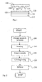
- a mould 100 has recesses 105 and protrusions 110 forming a nano structure pattern.
- the protrusions have the height of about 150 nm.
- the mould 100 can be made of any suitable material such as e.g. glass, silicon or metal such as nickel, as known to a person skilled in the art.
- the mould is coated with a thin anti-adhesive layer 190 (also referred to as antisticking layer) in form of a Teflon TM - like monolayer.
- the thickness of layer 190 is about 10 nm or less and can e.g. be obtained by chemical vapour deposition onto the stamp as known to a person skilled in the art.
- the substrate 115 is coated with a thin adhesive layer 120 (also referred to as sticking layer) consisting e.g. of 3-methacryl-oxypropyl-dimethyl-chlorosilane or hexamethyldisilane, HMDS.
- the layer 120 is preferably about 10 nm or less and can be obtained by e.g. spin coating.
- a forming layer (also referred to as an imprint resist layer) 125 is then provided on top of layer 120 and may consist of e.g. PMMA (PolyMethyl-Methacrylic Acid) and has a preferred thickness of about 150 nm.
- PMMA PolyMethyl-Methacrylic Acid
- the imprint PMMA layer 125 can be provided by using a suitable known technique such as spin coating.
- an anti-adhesive layer 130 is provided on top of imprint resist layer 125.
- the anti-adhesive layer 130 comprises tridecafluro- (1H,1H,2H,2H) tetrahydrooctylamine or similar partially or completely fluorinated compounds.
- the anti-adhesive layer 130 has preferably a thickness of 10 nm or less and can e.g. be spin coated on the imprint PMMA polymer layer 125, as a person skilled in the art realises.
- step 200 a mould 100 and a substrate 115 are prepared in accordance with the description above referring to figure 1 .
- the substrate 115 with the three layers 120, 125, 130 and the mould 100 are then heated above the glass transition temperature, causing the softening of layer 125.
- the pattern transfer is carried out by pressing the mould into the substrate coatings 120, 125, 130 using a gas pressure of about 5 to 100 bar, preferably about 30-60 bar, for ⁇ 300 sec., in accordance with a so called soft imprint method.
- the soft imprint method makes use of a pressure controlled chamber with a flexible membrane forming a counterstay for the substrate/mould for pressing the substrate and mould together with an even distribution of force between them.
- the soft imprint method is disclosed in the published international patent application WO01/42858 A1 .
- the forming layer 125 is solidified by cooling and curing in a known manner in step 225.
- the mould 100 is released from the substrate 115. In this way a structured nano-scale pattern is provided on the substrate by transferring an inverse pattern on the mould.
- the present invention overcomes the problems and drawbacks associated with known techniques by providing the substrate with an uppermost anti-adhesive layer on top of e.g. the imprint resist layer. This facilitates an even distribution of the anti-adhesive layer and also makes the evenness of the anti-adhesive layer less critical for the accuracy and fineness of the final imprint result.
- the invention provides a thin monolayer, such as a Teflon TM - like monolayer, as an anti-adhesive layer, on the mould.
- the thickness of the Teflon TM - like monolayer is about 10 nm or less according to the invention, however the thickness might vary depending on the chemistry applied.
- the imprint result shows a higher quality with practically no sticking of polymer to the mould surface and no release of polymer from the substrate. Furthermore, the imprint result indicates that the above problem regarding nonvertical sidewalls is alleviated. Thus, a nano pattern imprint method providing a higher accuracy, which also permits an economical mass production of even finer structures on a substrate has been disclosed.
Abstract
Description
- The present invention relates generally to the field of nanoimprint lithography and more specifically to methods and means for generating a nano-scale pattern on a substrate.
- Quantum devices whose performance is influenced by the materials being structured in the nanometer-scale e.g. single-electron devices, are promising for the coming electronic generations. Developments of nanofabrication technologies are essential for production of such nano-devices. In practice extreme e-beam lithography as well as AFM-based methods (Atomic Force Microscope) for manipulation of nano-particles have made it possible to fabricate structures and patterns with dimensions down to some few nanometers. However, those techniques are working in a serial manner preventing these nano lithographies to be applied for mass fabrication of devices. Nanoimprint lithography , (NIL) has the inherent potential to be a promising candidate for fabrication of such nanodevices in parallel. Here, a stamp patterned with a serial lithography technique, most often e-beam lithography, can be utilised for replications in a stamp-print approach, quite similar to the compact-disc (CD) manufacturing process. The CD production technique was introduced 1975, having shown it's excellent mass production capability. CD production has a total (worst case) yield better then 67% in the full area of each 6" compact disc being produced.
- Nanoimprint lithography (NIL) is a known technique for producing a nano scale pattern on a substrate. The substrate can e.g. be a semiconductor material, such as silicon, indium phosphide or gallium arsenide, and used e.g. for the production of semiconductor components. The substrate can also be of other materials such as ceramic materials, metals or polymers with a relatively high glass transition temperature, in case of other applications such as e.g. biosensors.
- The trend in microelectronics is towards ever smaller dimensions. In principle, development has been such that the dimensions are reduced to their half size about every third year. For instance, commercial components are manufactured today with structures of about 130 nm in size, but there is a need to go even further down in dimensions.
- The basic principle of NIL is mechanical deformation of a thin film layer, which is coated onto a flat plate of e.g. silicon. The NIL process can be compared with the production process for CD:s and can be described in three stages:
- 1. Production of a mould (i.e. a mould template): A mould can be produced from various materials, e.g. metal, semiconductor, ceramic or from certain plastics. To create a three-dimensional structure on one surface of the mould, various lithographic methods can be used, depending on the requirements for the size of the structures and their resolution. E-beam and X-ray lithography are normally used for structure dimensions that are less than 300 nm. Direct laser exposure and UV lithography are used for larger structures.
- 2. Imprint: A thin film layer of a polymer, e.g. polyamide, is applied to a flat substrate of silicon. The layer is heated to a certain temperature, the so-called imprint temperature. The mould and substrate are pressed together so that the inverse structure of the mould is transferred to the polymer layer on the substrate. During the imprint step, the resist is heated to a temperature above its glass transition temperature. At that temperature, the resist, which is thermoplastic, becomes a viscous liquid and can flow and, therefore, can be readily deformed into the shape of the mold. The resist's viscosity decreases as the temperature increases.
- 3. Structure transfer: In the areas pressed together in the polymer layer, a thin layer of polymer remains. The last stage is removal of this thin remaining layer on the substrate. This can be carried out in a so-called "RIB" or 02-plasma unit or in an anisotropic etching process, such as reactive ion etching, RIE. The thinner this remaining layer is, the finer the structures that can be created using the nanoimprint.
- A problem with conventional NIL procedures is that the mould can adhere to the thin film layer during pressing which makes the transferred inverse pattern in the thin film layer less accurate. Therefore, the mould is normally provided with a thin anti-adhesive layer in order to avoid such adhesion.
- The article "Step and Flash Imprint Lithography:A New Approach to High-Resolution Patterning", Proc. SPIE Vol. 3676, 379-389 (1999), by Willson et al, describes a polymer imprint resist layer with integrated anti-adhesive material in the polymer.
- Another imprint method uses imprint in combination with UV exposure to cure a polymer. This alternative approach to lithography is based on a bilayer imprint scheme. In this process, a standard quartz mask with a patterned chromium surface is reactive ion etched, producing high-resolution relief images in the surface. The remaining chromium is removed and the template is surface treated with a fluorinated self-assembled monolayer. A low-viscosity, photopolymerizable formulation is introduced into the gap between the two surfaces. The template is then brought into contact with the substrate. This solution, called the etch barrier, is photopolymerized by exposure through the backside of the quartz template. The template is separated from the substrate, leaving a UV-cured replica of the relief structure on the substrate. Features smaller than 40 nm in size have been reliably produced using this imprinting process. A problem/drawback with this technique is that it is not suitable for large area imprint without stepping and stamping/flashing, where the polymer has to be dispensed prior to each imprint step.
- There are several challenging problems associated with imprint lithography methods. One critical area is to perform the next level of processing while maintaining the same resolution demonstrated in the polymer layer. The formation of patterned metal layers is one application. Finely patterned metal layers are used as interconnects in integrated circuits. They can also be used as catalysts for subsequent layer growth. If the subsequent metal layers cannot readily be etched, e.g., due to crystal direction dependent etching rates, an additive approach such as lift-off is desirable. However, single polymer layers are problematic when transferring the pattern via metal lift-off. The nonvertical sidewalls resulting from the imprinting process result in tearing and detachment of the metal film during lift-off. Nonvertical sidewalls occur in imprint lithography if the imprinting element does not have vertical sidewalls. Even if the imprinter does have vertical sidewalls, nonvertical sidewalls are formed in the imprinted film due to a descumming step necessary to remove residual polymer from the bottom of the imprinted feature. Therefore, a technique is required that minimizes the problems associated with metal lift-off using single layer resists.
- There are other problems with those imprint techniques, which are addressed by the present invention such as changes in surface adhesion properties if substrate and organic materials are varied. This causes the process to be limited to polymer material in combination with specific substrate materials such as silicon, nickel, quartz, glass, silicon nitride etc. Using a release agent on the mold is not safe enough to be sure that the process can be used in industrial production.
- The document 'MULTILAYER RESIST METHODS FOR NANOIMPRINT LITHOGRAPHY ON NONFLAT SURFACES', by Sun X et al, published in "JUORNAL OF VACUUM SCIENCE AND TECHNOLOGY: PART B, AMERICAN INSTITUTE OF PHYSICS. NEW YORK, US, vol. 16, no 6, November 1998, discuss a flexible Nanoimprint lithography method wherein many materials can be used to achieve optimum results when imprinting on non flat surfaces. The document 'NANOIMPRINT LITHOGRAPHY OF HIGH-DENSITY COBALT DOT PATTERNS FOR FINE TUNING OF DIPOLE INTERACTIONS', by M. NATALI et al, published in J. Vac. Sci. Technol. B 19(6), Nov/Dec 2001, discuss a Nanoimprint lithography method using hybrane as the top layer resist which gives better dimensional control of the replicated patterns compared to PMMA (Polymethylmethacrylate).
- It thus exists a need to find nano imprint litography methods and means providing the possibility to transfer even finer nano-scale structures from a mould to a substrate in an economical way and eliminating/alleviating the problem concerning adhesion of the mould to the substrate during imprinting.
- The object of the present invention is to eliminate/alleviate above drawbacks/problems.
- One object of the present invention is thus to find nano imprint litography methods and means providing the possibility to transfer even finer nano-scale structures from a mould to a substrate.
- Another object of the present invention is to find nano imprint litography methods and means, which alleviate the problem concerning adhesion of the mould to the substrate during imprinting.
- Still another object of the present invention is to find nano imprint litography methods and means, which improve the accuracy of the imprint pattern on the substrate.
- A further object of the present invention is to provide nano imprint litography methods and means which improves imprinting quality by reducing the sticking of polymer on to the mould surface and the release of polymer from the substrate.
- Still a further object of the present invention is to provide nano imprint litography methods and means which provide the possibility of economical mass production of nano-structures of higher accuracy.
- According to one aspect of the present invention, the invention accomplishes above objects by a method for forming a structured pattern on a substrate wherein said substrate is coated with a plurality of coating layers before pressing, where each coating layer has a specific function and
- the uppermost coating layer on top of the substrate has a pure anti-adhesive function.
- According still another aspect of the invention, a substrate is provided for forming a nano scale pattern on said substrate wherein said substrate is coated with a plurality of coating layers each having a specific function and the substrate has an uppermost coating layer having a pure anti-adhesive function.
- Although the present invention has been summarised above, the present invention is defined by the independent claims 1 and 8. Further embodiments of the invention are defined by the dependent claims 2-7, 9-11.
-
-
Figure 1 illustrates a substrate and mould for forming a nano scale pattern according to the invention. -
Figure 2 illustrates a flow chart for a method for providing a nano scale pattern on a substrate, which can be used to carry out the invention. - The present invention is based on the identification of problems/drawbacks with integrating an anti-adhesive material in the polymer imprint resist layer on the substrate during nano-imprint lithography, as described e.g. in the above mentioned article "Step and Flash Imprint Lithography:A New Approach to High-Resolution Patterning", Proc. SPIE Vol. 3676, 379-389 (1999), by Willson et al, describes a polymer imprint resist layer with integrated anti-adhesive material in the polymer. This approach gives far from optimal antisticking performance, leading to sticking of polymer to the mould and as a consequence hinders an economical mass production of even fmer nano-scale patterns on substrates.
- The present invention is illustrated in
figure 1 . Amould 100 hasrecesses 105 andprotrusions 110 forming a nano structure pattern. The protrusions have the height of about 150 nm. Themould 100 can be made of any suitable material such as e.g. glass, silicon or metal such as nickel, as known to a person skilled in the art. According to a preferred embodiment, the mould is coated with a thin anti-adhesive layer 190 (also referred to as antisticking layer) in form of a Teflon TM - like monolayer. The thickness of layer 190 is about 10 nm or less and can e.g. be obtained by chemical vapour deposition onto the stamp as known to a person skilled in the art. Asubstrate 115 made of any suitable material such as e.g. silicon (or silicon glass) as known to a person skilled in the art, is provided. Thesubstrate 115 is coated with a thin adhesive layer 120 (also referred to as sticking layer) consisting e.g. of 3-methacryl-oxypropyl-dimethyl-chlorosilane or hexamethyldisilane, HMDS. Thelayer 120 is preferably about 10 nm or less and can be obtained by e.g. spin coating. A forming layer (also referred to as an imprint resist layer) 125 is then provided on top oflayer 120 and may consist of e.g. PMMA (PolyMethyl-Methacrylic Acid) and has a preferred thickness of about 150 nm. Theimprint PMMA layer 125 can be provided by using a suitable known technique such as spin coating. According to the invention, ananti-adhesive layer 130 is provided on top of imprint resistlayer 125. Theanti-adhesive layer 130 comprises tridecafluro- (1H,1H,2H,2H) tetrahydrooctylamine or similar partially or completely fluorinated compounds. Theanti-adhesive layer 130 has preferably a thickness of 10 nm or less and can e.g. be spin coated on the imprintPMMA polymer layer 125, as a person skilled in the art realises. - Referring to
figure 2 a flow chart for the nano-imprint method according to the present invention is illustrated. Instep 200, amould 100 and asubstrate 115 are prepared in accordance with the description above referring tofigure 1 . Instep 210, thesubstrate 115 with the threelayers mould 100 are then heated above the glass transition temperature, causing the softening oflayer 125. Instep 220, the pattern transfer is carried out by pressing the mould into thesubstrate coatings published international patent application WO01/42858 A1 layer 125 is solidified by cooling and curing in a known manner instep 225. Instep 230, themould 100 is released from thesubstrate 115. In this way a structured nano-scale pattern is provided on the substrate by transferring an inverse pattern on the mould. - The present invention overcomes the problems and drawbacks associated with known techniques by providing the substrate with an uppermost anti-adhesive layer on top of e.g. the imprint resist layer. This facilitates an even distribution of the anti-adhesive layer and also makes the evenness of the anti-adhesive layer less critical for the accuracy and fineness of the final imprint result. The invention provides a thin monolayer, such as a Teflon TM - like monolayer, as an anti-adhesive layer, on the mould. The thickness of the Teflon TM - like monolayer is about 10 nm or less according to the invention, however the thickness might vary depending on the chemistry applied.
- By using the imprint technique according to the invention, the imprint result shows a higher quality with practically no sticking of polymer to the mould surface and no release of polymer from the substrate. Furthermore, the imprint result indicates that the above problem regarding nonvertical sidewalls is alleviated. Thus, a nano pattern imprint method providing a higher accuracy, which also permits an economical mass production of even finer structures on a substrate has been disclosed.
- The invention has been described by means of illustrative examples. The figures are not to scale but illustrate merely the working principle of the invention. Many modifications are possible for a person skilled in the art, e.g. regarding additional functional layers, e.g. to introduce a so called lift-off layer etc, between the
substrate 115 and theanti-adhesive layer 130 without departing from the scope of the invention as defined by the following claims.
Claims (11)
- A nanoimprint lithography method for providing a structured nano scale pattern on a substrate (115) by transferring an inverse pattern from a mould (100) to said substrate (115) by pressing said mould and substrate together, said substrate being coated with a plurality of coating layers, comprising an imprint resist layer (125), said method characterised in that it comprises the step of:- providing an uppermost coating layer (130) on top of the substrate having a pure anti-adhesive function before pressing.
- The method of claim 1 further comprising the step of:- providing a sticking layer (120) disposed under said imprint resist layer (125), before pressing.
- The method according to claim 1 further comprising the step of:- forming said anti-adhesive layer (130) so it comprises partially fluorinated compounds.
- The method according to claim 1 further comprising the step of:- forming said anti-adhesive layer (130) so it comprises completely fluorinated compounds.
- The method according to claim 1 further comprising the step of:- forming said anti-adhesive layer (130) so it comprises tridecafluro-(1H,1H,2H,2H) tetrahydrooctylamine.
- The method according to claim 1 further comprising the step of:- providing an anti-adhesive layer (190) on said mould before pressing.
- The method according to claim 1 further comprising the step of:- providing a substantially even distribution of force between said substrate and mould by using a pressure controlled chamber having a flexible membrane on which said substrate or mould is disposed during the transfer of said pattern to said substrate (115).
- A substrate (115) devised for forming a nano scale pattern on said substrate by means of nanoimprint lithography, said substrate (115) being coated with a plurality of coating layers, comprising an imprint resist layer (125), characterised in that the uppermost coating layer (130) on top of the substrate is formed by a compound giving it a pure anti-adhesive function.
- The substrate according to claim 8, wherein said anti-adhesive layer (130) comprises a partially fluorinated compound.
- The substrate according to claim 8, wherein said anti-adhesive layer (130) comprises a completely fluorinated compound.
- The substrate according to claim 9, wherein said anti-adhesive layer (130) comprises tridecafluro- (1H,1H,2H,2H) tetrahydrooctylamine.
Priority Applications (7)
| Application Number | Priority Date | Filing Date | Title |
|---|---|---|---|
| DE60336322T DE60336322D1 (en) | 2003-11-21 | 2003-11-21 | Nanoimprint lithography in multilayer systems |
| EP03078683A EP1533657B1 (en) | 2003-11-21 | 2003-11-21 | Multilayer nano imprint lithography |
| AT03078683T ATE501464T1 (en) | 2003-11-21 | 2003-11-21 | NANOIMPRINT LITHOGRAPHY IN A MULTI-LAYER SYSTEM |
| US10/992,322 US20060040058A1 (en) | 2003-11-21 | 2004-11-19 | Multilayer nano imprint lithography |
| CN 200410095336 CN1619417A (en) | 2003-11-21 | 2004-11-19 | Multilayer nano imprint lithography |
| JP2004338054A JP3892457B2 (en) | 2003-11-21 | 2004-11-22 | Nanoimprint lithography method and substrate |
| US12/007,750 US20080138460A1 (en) | 2003-11-21 | 2008-01-15 | Multilayer nano imprint lithography |
Applications Claiming Priority (1)
| Application Number | Priority Date | Filing Date | Title |
|---|---|---|---|
| EP03078683A EP1533657B1 (en) | 2003-11-21 | 2003-11-21 | Multilayer nano imprint lithography |
Publications (2)
| Publication Number | Publication Date |
|---|---|
| EP1533657A1 EP1533657A1 (en) | 2005-05-25 |
| EP1533657B1 true EP1533657B1 (en) | 2011-03-09 |
Family
ID=34429454
Family Applications (1)
| Application Number | Title | Priority Date | Filing Date |
|---|---|---|---|
| EP03078683A Expired - Lifetime EP1533657B1 (en) | 2003-11-21 | 2003-11-21 | Multilayer nano imprint lithography |
Country Status (4)
| Country | Link |
|---|---|
| US (2) | US20060040058A1 (en) |
| EP (1) | EP1533657B1 (en) |
| AT (1) | ATE501464T1 (en) |
| DE (1) | DE60336322D1 (en) |
Cited By (3)
| Publication number | Priority date | Publication date | Assignee | Title |
|---|---|---|---|---|
| US8557351B2 (en) | 2005-07-22 | 2013-10-15 | Molecular Imprints, Inc. | Method for adhering materials together |
| US8808808B2 (en) | 2005-07-22 | 2014-08-19 | Molecular Imprints, Inc. | Method for imprint lithography utilizing an adhesion primer layer |
| US20220390839A1 (en) * | 2021-06-03 | 2022-12-08 | Viavi Solutions Inc. | Method of replicating a microstructure pattern |
Families Citing this family (24)
| Publication number | Priority date | Publication date | Assignee | Title |
|---|---|---|---|---|
| US9040090B2 (en) | 2003-12-19 | 2015-05-26 | The University Of North Carolina At Chapel Hill | Isolated and fixed micro and nano structures and methods thereof |
| CA2847260C (en) | 2003-12-19 | 2016-06-21 | The University Of North Carolina At Chapel Hill | Methods for fabricating isolated micro- and nano- structures using soft or imprint lithography |
| JP4290177B2 (en) * | 2005-06-08 | 2009-07-01 | キヤノン株式会社 | Mold, alignment method, pattern forming apparatus, pattern transfer apparatus, and chip manufacturing method |
| CN101604124B (en) * | 2005-06-08 | 2011-07-27 | 佳能株式会社 | Mold, pattern forming method, and pattern forming apparatus |
| EP1731962B1 (en) | 2005-06-10 | 2008-12-31 | Obducat AB | Pattern replication with intermediate stamp |
| US7854873B2 (en) | 2005-06-10 | 2010-12-21 | Obducat Ab | Imprint stamp comprising cyclic olefin copolymer |
| US8846195B2 (en) | 2005-07-22 | 2014-09-30 | Canon Nanotechnologies, Inc. | Ultra-thin polymeric adhesion layer |
| US7759407B2 (en) | 2005-07-22 | 2010-07-20 | Molecular Imprints, Inc. | Composition for adhering materials together |
| WO2007046110A1 (en) * | 2005-10-19 | 2007-04-26 | Indian Institute Of Technology, Kanpur | A method and apparatus for the formation of patterns on surfaces and an assembly and alignment of the structure thereof |
| US7862756B2 (en) * | 2006-03-30 | 2011-01-04 | Asml Netherland B.V. | Imprint lithography |
| US7780431B2 (en) * | 2006-09-14 | 2010-08-24 | Hewlett-Packard Development Company, L.P. | Nanoimprint molds and methods of forming the same |
| KR101479804B1 (en) * | 2007-09-13 | 2015-01-06 | 아사히 가라스 가부시키가이샤 | TiO2-CONTAINING QUARTZ GLASS SUBSTRATE |
| US20110236639A1 (en) * | 2008-07-17 | 2011-09-29 | Agency For Science, Technology And Research | Method of making an imprint on a polymer structure |
| US8361546B2 (en) | 2008-10-30 | 2013-01-29 | Molecular Imprints, Inc. | Facilitating adhesion between substrate and patterned layer |
| EP2199854B1 (en) | 2008-12-19 | 2015-12-16 | Obducat AB | Hybrid polymer mold for nano-imprinting and method for making the same |
| EP2199855B1 (en) | 2008-12-19 | 2016-07-20 | Obducat | Methods and processes for modifying polymer material surface interactions |
| WO2011066450A2 (en) * | 2009-11-24 | 2011-06-03 | Molecular Imprints, Inc. | Adhesion layers in nanoimprint lithography |
| WO2013010111A2 (en) | 2011-07-13 | 2013-01-17 | University Of Utah Research Foundation | Nanoimprint lithography |
| KR20150053960A (en) * | 2012-09-06 | 2015-05-19 | 더 리전츠 오브 더 유니버시티 오브 콜로라도, 어 바디 코퍼레이트 | Filtration membranes with nanoscale patterns |
| DE102012112550A1 (en) * | 2012-12-18 | 2014-06-18 | Lpkf Laser & Electronics Ag | Method for metallizing a workpiece and a layer structure of a workpiece and a metal layer |
| CN104625559B (en) * | 2015-01-08 | 2017-03-15 | 哈尔滨工业大学 | A kind of metal subfebrile temperature in pression forming die device and method |
| ES2901424T3 (en) * | 2017-03-16 | 2022-03-22 | Univ Aix Marseille | Nanoimprint lithography process and substrate with pattern obtainable from it |
| CN108931884A (en) * | 2017-05-27 | 2018-12-04 | 蓝思科技(长沙)有限公司 | Imprint membrane and imprinting apparatus |
| CN117295560A (en) * | 2021-04-30 | 2023-12-26 | 奇跃公司 | Imprint lithography process and method on curved surfaces |
Family Cites Families (11)
| Publication number | Priority date | Publication date | Assignee | Title |
|---|---|---|---|---|
| US3972924A (en) * | 1975-03-24 | 1976-08-03 | The United States Of America As Represented By The Secretary Of Agriculture | 1-(1H,1H-perfluorooctyl)-1,3-trimethylenediphosphonic tetrachloride |
| US5277788A (en) * | 1990-10-01 | 1994-01-11 | Aluminum Company Of America | Twice-anodized aluminum article having an organo-phosphorus monolayer and process for making the article |
| US6309580B1 (en) * | 1995-11-15 | 2001-10-30 | Regents Of The University Of Minnesota | Release surfaces, particularly for use in nanoimprint lithography |
| US6284345B1 (en) * | 1997-12-08 | 2001-09-04 | Washington University | Designer particles of micron and submicron dimension |
| US6517995B1 (en) * | 1999-09-14 | 2003-02-11 | Massachusetts Institute Of Technology | Fabrication of finely featured devices by liquid embossing |
| SE515607C2 (en) * | 1999-12-10 | 2001-09-10 | Obducat Ab | Device and method for fabrication of structures |
| DE60121302T2 (en) * | 2000-01-21 | 2007-06-28 | Obducat Ab | FORM FOR NANOBE PRINTING |
| JP2002270541A (en) * | 2001-03-08 | 2002-09-20 | Matsushita Electric Ind Co Ltd | Mold method of manufacturing mold, and method of forming pattern |
| US6991809B2 (en) * | 2001-06-23 | 2006-01-31 | Lyotropic Therapeutics, Inc. | Particles with improved solubilization capacity |
| US20030017424A1 (en) * | 2001-07-18 | 2003-01-23 | Miri Park | Method and apparatus for fabricating complex grating structures |
| US6824882B2 (en) * | 2002-05-31 | 2004-11-30 | 3M Innovative Properties Company | Fluorinated phosphonic acids |
-
2003
- 2003-11-21 EP EP03078683A patent/EP1533657B1/en not_active Expired - Lifetime
- 2003-11-21 AT AT03078683T patent/ATE501464T1/en not_active IP Right Cessation
- 2003-11-21 DE DE60336322T patent/DE60336322D1/en not_active Expired - Lifetime
-
2004
- 2004-11-19 US US10/992,322 patent/US20060040058A1/en not_active Abandoned
-
2008
- 2008-01-15 US US12/007,750 patent/US20080138460A1/en not_active Abandoned
Cited By (3)
| Publication number | Priority date | Publication date | Assignee | Title |
|---|---|---|---|---|
| US8557351B2 (en) | 2005-07-22 | 2013-10-15 | Molecular Imprints, Inc. | Method for adhering materials together |
| US8808808B2 (en) | 2005-07-22 | 2014-08-19 | Molecular Imprints, Inc. | Method for imprint lithography utilizing an adhesion primer layer |
| US20220390839A1 (en) * | 2021-06-03 | 2022-12-08 | Viavi Solutions Inc. | Method of replicating a microstructure pattern |
Also Published As
| Publication number | Publication date |
|---|---|
| EP1533657A1 (en) | 2005-05-25 |
| ATE501464T1 (en) | 2011-03-15 |
| DE60336322D1 (en) | 2011-04-21 |
| US20080138460A1 (en) | 2008-06-12 |
| US20060040058A1 (en) | 2006-02-23 |
Similar Documents
| Publication | Publication Date | Title |
|---|---|---|
| EP1533657B1 (en) | Multilayer nano imprint lithography | |
| US6964793B2 (en) | Method for fabricating nanoscale patterns in light curable compositions using an electric field | |
| Guo | Nanoimprint lithography: methods and material requirements | |
| US7114938B2 (en) | Lithographic apparatus for molding ultrafine features | |
| US7699598B2 (en) | Conforming template for patterning liquids disposed on substrates | |
| EP1656242B1 (en) | Capillary imprinting technique | |
| US20030080472A1 (en) | Lithographic method with bonded release layer for molding small patterns | |
| Choi et al. | A soft-imprint technique for direct fabrication of submicron scale patterns using a surface-modified PDMS mold | |
| US20070059497A1 (en) | Reversal imprint technique | |
| WO2006073874A2 (en) | Release layer comprising diamond-like carbon (dlc) or doped dlc with tunable composition | |
| EP2470956B1 (en) | Functional nanoparticles | |
| US20080217813A1 (en) | Release surfaces, particularly for use in nanoimprint lithography | |
| JP3892457B2 (en) | Nanoimprint lithography method and substrate | |
| KR100693992B1 (en) | Nickel stamp structure for providing easy formation of self-assembled monolayer as anti-stiction layer, and manufacturing method thereof | |
| US20100109194A1 (en) | Master Template Replication | |
| EP1512048B1 (en) | Method for fabricating nanoscale patterns in light curable compositions using an electric field | |
| Mohamed | 2.16 Nanoimprint Lithography for Nanomanufacturing | |
| Tiginyanu et al. | Nanoimprint lithography (NIL) and related techniques for electronics applications | |
| US20050082253A1 (en) | Applying imprinting material to substrates employing electromagnetic fields | |
| Cui et al. | Nanofabrication by Replication | |
| Nakamatsu et al. | Room-temperature nanoimprint lithography using photosensitive dry film | |
| Pabba | Evaluation of processes in nanoimprint lithography | |
| Schift et al. | Nanoimprint |
Legal Events
| Date | Code | Title | Description |
|---|---|---|---|
| PUAI | Public reference made under article 153(3) epc to a published international application that has entered the european phase |
Free format text: ORIGINAL CODE: 0009012 |
|
| 17P | Request for examination filed |
Effective date: 20041203 |
|
| AK | Designated contracting states |
Kind code of ref document: A1 Designated state(s): AT BE BG CH CY CZ DE DK EE ES FI FR GB GR HU IE IT LI LU MC NL PT RO SE SI SK TR |
|
| AX | Request for extension of the european patent |
Extension state: AL LT LV MK |
|
| AKX | Designation fees paid |
Designated state(s): AT BE BG CH CY CZ DE DK EE ES FI FR GB GR HU IE IT LI LU MC NL PT RO SE SI SK TR |
|
| GRAP | Despatch of communication of intention to grant a patent |
Free format text: ORIGINAL CODE: EPIDOSNIGR1 |
|
| GRAS | Grant fee paid |
Free format text: ORIGINAL CODE: EPIDOSNIGR3 |
|
| GRAA | (expected) grant |
Free format text: ORIGINAL CODE: 0009210 |
|
| AK | Designated contracting states |
Kind code of ref document: B1 Designated state(s): AT BE BG CH CY CZ DE DK EE ES FI FR GB GR HU IE IT LI LU MC NL PT RO SE SI SK TR |
|
| REG | Reference to a national code |
Ref country code: GB Ref legal event code: FG4D |
|
| REG | Reference to a national code |
Ref country code: CH Ref legal event code: EP |
|
| REG | Reference to a national code |
Ref country code: IE Ref legal event code: FG4D |
|
| REF | Corresponds to: |
Ref document number: 60336322 Country of ref document: DE Date of ref document: 20110421 Kind code of ref document: P |
|
| REG | Reference to a national code |
Ref country code: DE Ref legal event code: R096 Ref document number: 60336322 Country of ref document: DE Effective date: 20110421 |
|
| REG | Reference to a national code |
Ref country code: NL Ref legal event code: VDEP Effective date: 20110309 |
|
| PG25 | Lapsed in a contracting state [announced via postgrant information from national office to epo] |
Ref country code: GR Free format text: LAPSE BECAUSE OF FAILURE TO SUBMIT A TRANSLATION OF THE DESCRIPTION OR TO PAY THE FEE WITHIN THE PRESCRIBED TIME-LIMIT Effective date: 20110610 Ref country code: ES Free format text: LAPSE BECAUSE OF FAILURE TO SUBMIT A TRANSLATION OF THE DESCRIPTION OR TO PAY THE FEE WITHIN THE PRESCRIBED TIME-LIMIT Effective date: 20110620 Ref country code: SE Free format text: LAPSE BECAUSE OF FAILURE TO SUBMIT A TRANSLATION OF THE DESCRIPTION OR TO PAY THE FEE WITHIN THE PRESCRIBED TIME-LIMIT Effective date: 20110309 |
|
| PG25 | Lapsed in a contracting state [announced via postgrant information from national office to epo] |
Ref country code: FI Free format text: LAPSE BECAUSE OF FAILURE TO SUBMIT A TRANSLATION OF THE DESCRIPTION OR TO PAY THE FEE WITHIN THE PRESCRIBED TIME-LIMIT Effective date: 20110309 Ref country code: BG Free format text: LAPSE BECAUSE OF FAILURE TO SUBMIT A TRANSLATION OF THE DESCRIPTION OR TO PAY THE FEE WITHIN THE PRESCRIBED TIME-LIMIT Effective date: 20110609 Ref country code: CY Free format text: LAPSE BECAUSE OF FAILURE TO SUBMIT A TRANSLATION OF THE DESCRIPTION OR TO PAY THE FEE WITHIN THE PRESCRIBED TIME-LIMIT Effective date: 20110309 Ref country code: NL Free format text: LAPSE BECAUSE OF FAILURE TO SUBMIT A TRANSLATION OF THE DESCRIPTION OR TO PAY THE FEE WITHIN THE PRESCRIBED TIME-LIMIT Effective date: 20110309 Ref country code: AT Free format text: LAPSE BECAUSE OF FAILURE TO SUBMIT A TRANSLATION OF THE DESCRIPTION OR TO PAY THE FEE WITHIN THE PRESCRIBED TIME-LIMIT Effective date: 20110309 Ref country code: SI Free format text: LAPSE BECAUSE OF FAILURE TO SUBMIT A TRANSLATION OF THE DESCRIPTION OR TO PAY THE FEE WITHIN THE PRESCRIBED TIME-LIMIT Effective date: 20110309 |
|
| PG25 | Lapsed in a contracting state [announced via postgrant information from national office to epo] |
Ref country code: BE Free format text: LAPSE BECAUSE OF FAILURE TO SUBMIT A TRANSLATION OF THE DESCRIPTION OR TO PAY THE FEE WITHIN THE PRESCRIBED TIME-LIMIT Effective date: 20110309 |
|
| PG25 | Lapsed in a contracting state [announced via postgrant information from national office to epo] |
Ref country code: EE Free format text: LAPSE BECAUSE OF FAILURE TO SUBMIT A TRANSLATION OF THE DESCRIPTION OR TO PAY THE FEE WITHIN THE PRESCRIBED TIME-LIMIT Effective date: 20110309 Ref country code: PT Free format text: LAPSE BECAUSE OF FAILURE TO SUBMIT A TRANSLATION OF THE DESCRIPTION OR TO PAY THE FEE WITHIN THE PRESCRIBED TIME-LIMIT Effective date: 20110711 |
|
| PG25 | Lapsed in a contracting state [announced via postgrant information from national office to epo] |
Ref country code: RO Free format text: LAPSE BECAUSE OF FAILURE TO SUBMIT A TRANSLATION OF THE DESCRIPTION OR TO PAY THE FEE WITHIN THE PRESCRIBED TIME-LIMIT Effective date: 20110309 Ref country code: SK Free format text: LAPSE BECAUSE OF FAILURE TO SUBMIT A TRANSLATION OF THE DESCRIPTION OR TO PAY THE FEE WITHIN THE PRESCRIBED TIME-LIMIT Effective date: 20110309 Ref country code: CZ Free format text: LAPSE BECAUSE OF FAILURE TO SUBMIT A TRANSLATION OF THE DESCRIPTION OR TO PAY THE FEE WITHIN THE PRESCRIBED TIME-LIMIT Effective date: 20110309 |
|
| PLBE | No opposition filed within time limit |
Free format text: ORIGINAL CODE: 0009261 |
|
| STAA | Information on the status of an ep patent application or granted ep patent |
Free format text: STATUS: NO OPPOSITION FILED WITHIN TIME LIMIT |
|
| 26N | No opposition filed |
Effective date: 20111212 |
|
| PG25 | Lapsed in a contracting state [announced via postgrant information from national office to epo] |
Ref country code: DK Free format text: LAPSE BECAUSE OF FAILURE TO SUBMIT A TRANSLATION OF THE DESCRIPTION OR TO PAY THE FEE WITHIN THE PRESCRIBED TIME-LIMIT Effective date: 20110309 |
|
| REG | Reference to a national code |
Ref country code: DE Ref legal event code: R097 Ref document number: 60336322 Country of ref document: DE Effective date: 20111212 |
|
| PG25 | Lapsed in a contracting state [announced via postgrant information from national office to epo] |
Ref country code: IT Free format text: LAPSE BECAUSE OF FAILURE TO SUBMIT A TRANSLATION OF THE DESCRIPTION OR TO PAY THE FEE WITHIN THE PRESCRIBED TIME-LIMIT Effective date: 20110309 |
|
| PG25 | Lapsed in a contracting state [announced via postgrant information from national office to epo] |
Ref country code: MC Free format text: LAPSE BECAUSE OF NON-PAYMENT OF DUE FEES Effective date: 20111130 |
|
| REG | Reference to a national code |
Ref country code: CH Ref legal event code: PL |
|
| GBPC | Gb: european patent ceased through non-payment of renewal fee |
Effective date: 20111121 |
|
| PG25 | Lapsed in a contracting state [announced via postgrant information from national office to epo] |
Ref country code: LI Free format text: LAPSE BECAUSE OF NON-PAYMENT OF DUE FEES Effective date: 20111130 Ref country code: CH Free format text: LAPSE BECAUSE OF NON-PAYMENT OF DUE FEES Effective date: 20111130 |
|
| REG | Reference to a national code |
Ref country code: IE Ref legal event code: MM4A |
|
| PG25 | Lapsed in a contracting state [announced via postgrant information from national office to epo] |
Ref country code: IE Free format text: LAPSE BECAUSE OF NON-PAYMENT OF DUE FEES Effective date: 20111121 Ref country code: GB Free format text: LAPSE BECAUSE OF NON-PAYMENT OF DUE FEES Effective date: 20111121 |
|
| PG25 | Lapsed in a contracting state [announced via postgrant information from national office to epo] |
Ref country code: LU Free format text: LAPSE BECAUSE OF NON-PAYMENT OF DUE FEES Effective date: 20111121 |
|
| PG25 | Lapsed in a contracting state [announced via postgrant information from national office to epo] |
Ref country code: TR Free format text: LAPSE BECAUSE OF FAILURE TO SUBMIT A TRANSLATION OF THE DESCRIPTION OR TO PAY THE FEE WITHIN THE PRESCRIBED TIME-LIMIT Effective date: 20110309 |
|
| PG25 | Lapsed in a contracting state [announced via postgrant information from national office to epo] |
Ref country code: HU Free format text: LAPSE BECAUSE OF FAILURE TO SUBMIT A TRANSLATION OF THE DESCRIPTION OR TO PAY THE FEE WITHIN THE PRESCRIBED TIME-LIMIT Effective date: 20110309 |
|
| REG | Reference to a national code |
Ref country code: FR Ref legal event code: PLFP Year of fee payment: 13 |
|
| REG | Reference to a national code |
Ref country code: FR Ref legal event code: PLFP Year of fee payment: 14 |
|
| REG | Reference to a national code |
Ref country code: FR Ref legal event code: PLFP Year of fee payment: 15 |
|
| REG | Reference to a national code |
Ref country code: FR Ref legal event code: PLFP Year of fee payment: 16 |
|
| PGFP | Annual fee paid to national office [announced via postgrant information from national office to epo] |
Ref country code: DE Payment date: 20191105 Year of fee payment: 17 |
|
| PGFP | Annual fee paid to national office [announced via postgrant information from national office to epo] |
Ref country code: FR Payment date: 20191023 Year of fee payment: 17 |
|
| REG | Reference to a national code |
Ref country code: DE Ref legal event code: R119 Ref document number: 60336322 Country of ref document: DE |
|
| PG25 | Lapsed in a contracting state [announced via postgrant information from national office to epo] |
Ref country code: FR Free format text: LAPSE BECAUSE OF NON-PAYMENT OF DUE FEES Effective date: 20201130 |
|
| PG25 | Lapsed in a contracting state [announced via postgrant information from national office to epo] |
Ref country code: DE Free format text: LAPSE BECAUSE OF NON-PAYMENT OF DUE FEES Effective date: 20210601 |