EP1535699A1 - Polishing pad with high optical transmission window - Google Patents
Polishing pad with high optical transmission window Download PDFInfo
- Publication number
- EP1535699A1 EP1535699A1 EP04257057A EP04257057A EP1535699A1 EP 1535699 A1 EP1535699 A1 EP 1535699A1 EP 04257057 A EP04257057 A EP 04257057A EP 04257057 A EP04257057 A EP 04257057A EP 1535699 A1 EP1535699 A1 EP 1535699A1
- Authority
- EP
- European Patent Office
- Prior art keywords
- diisocyanate
- polishing pad
- window
- hexamethylene
- curing agent
- Prior art date
- Legal status (The legal status is an assumption and is not a legal conclusion. Google has not performed a legal analysis and makes no representation as to the accuracy of the status listed.)
- Granted
Links
Images
Classifications
-
- B—PERFORMING OPERATIONS; TRANSPORTING
- B24—GRINDING; POLISHING
- B24D—TOOLS FOR GRINDING, BUFFING OR SHARPENING
- B24D3/00—Physical features of abrasive bodies, or sheets, e.g. abrasive surfaces of special nature; Abrasive bodies or sheets characterised by their constituents
- B24D3/02—Physical features of abrasive bodies, or sheets, e.g. abrasive surfaces of special nature; Abrasive bodies or sheets characterised by their constituents the constituent being used as bonding agent
- B24D3/20—Physical features of abrasive bodies, or sheets, e.g. abrasive surfaces of special nature; Abrasive bodies or sheets characterised by their constituents the constituent being used as bonding agent and being essentially organic
-
- B—PERFORMING OPERATIONS; TRANSPORTING
- B24—GRINDING; POLISHING
- B24B—MACHINES, DEVICES, OR PROCESSES FOR GRINDING OR POLISHING; DRESSING OR CONDITIONING OF ABRADING SURFACES; FEEDING OF GRINDING, POLISHING, OR LAPPING AGENTS
- B24B37/00—Lapping machines or devices; Accessories
- B24B37/11—Lapping tools
- B24B37/20—Lapping pads for working plane surfaces
- B24B37/205—Lapping pads for working plane surfaces provided with a window for inspecting the surface of the work being lapped
Abstract
Description
- The present invention relates to polishing pads for chemical mechanical planarization (CMP), and in particular, relates to polishing pads having windows formed therein for performing optical end-point detection.
- In the fabrication of integrated circuits and other electronic devices, multiple layers of conducting, semiconducting and dielectric materials are deposited on or removed from a surface of a semiconductor wafer. Thin layers of conducting, semiconducting, and dielectric materials may be deposited by a number of deposition techniques. Common deposition techniques in modern processing include physical vapor deposition (PVD), also known as sputtering, chemical vapor deposition (CVD), plasma-enhanced chemical vapor deposition (PECVD), and electrochemical plating (ECP).
- As layers of materials are sequentially deposited and removed, the uppermost surface of the wafer becomes non-planar. Because subsequent semiconductor processing (e.g., metallization) requires the wafer to have a flat surface, the wafer needs to be planarized. Planarization is useful in removing undesired surface topography and surface defects, such as rough surfaces, agglomerated materials, crystal lattice damage, scratches, and contaminated layers or materials.
- Chemical mechanical planarization, or chemical mechanical polishing (CMP), is a common technique used to planarize substrates, such as semiconductor wafers. In conventional CMP, a wafer carrier is mounted on a carrier assembly and positioned in contact with a polishing pad in a CMP apparatus. The carrier assembly provides a controllable pressure to the wafer, urging it against the polishing pad. The pad is optionally moved (e.g., rotated) relative to the wafer by an external driving force. Simultaneously therewith, a chemical composition ("slurry") or other fluid medium is flowed onto the polishing pad and into the gap between the wafer and the polishing pad. The wafer surface is thus polished and made planar by the chemical and mechanical action of the pad surface and slurry.
- An important step in planarizing a wafer is determining an end-point to the process. Accordingly, a variety of planarization end-point detection methods have been developed, for example, methods involving optical in-situ measurements of the wafer surface. The optical technique involves providing the polishing pad with a window to select wavelengths of light. A light beam is directed through the window to the wafer surface, where it reflects and passes back through the window to a detector (e.g., a spectrophotometer). Based on the return signal, properties of the wafer surface (e.g., the thickness of films) can be determined for end-point detection.
- Birang et al., in U.S. Patent No. 6,280,290, discloses a polishing pad having a window in the form of a polyurethane plug. The pad has an aperture and the window is held in the aperture with adhesives. Unfortunately, these prior art windows have light transmission properties that hamper effective endpoint detection or measurement for a wide variety of planarizing conditions. This is due, in part, to the high degree of crystallinity of aromatic diisocyanate-based materials, such as, toluene diisocyanate (TDI), diphenylmethane (MDI) and its derivatives. These aromatic diisocyanates (TDI, MDI) are the two most commonly used in polyurethane manufacture. Furthermore, the use of aromatic diamine curatives, such as methylene bis 2-chloroaniline (MBOCA), increase crystallinity. Also, curatives such as MBOCA are colored, typically yellow to green, and impart a color to (i.e., cause absorption in) the finished polymer.
- For example, typical prior art windows provide only about 50% transmission at 450 nm, and to just over 40% at 430 nm. At 400 nm, the transmission steeply declines to about 13% making robust in-situ endpoint detection or measurement difficult. This is particularly problematic due to the demand for shorter wavelength endpoint detection requirements (e.g., at 400 nm).
- Hence, what is needed is a polishing pad and method for robust end-point detection or measurement during CMP over a wide range of wavelengths, and in particular, the shorter wavelengths. Also, there is a need for a polishing pad and method that can reduce the use of curatives.
- The present invention provides a chemical mechanical polishing pad comprising a window formed therein, wherein the window is formed from an aliphatic polyisocyanate-containing material. In particular, the window is formed from a reaction of an aliphatic polyisocyanate, a hydroxyl-containing material and a curing agent. The window of the present invention shows unexpected, improved transmission of laser signals for end-point detection during chemical mechanical polishing processes.
- In a first aspect of the present invention, there is provided a chemical mechanical polishing pad comprising: a polishing pad having a window for end-point detection formed therein; and wherein the window is formed from a reaction of an aliphatic polyisocyanate, a hydroxyl-containing material and a curing agent.
- In a second aspect of the present invention, there is provided an apparatus for chemical mechanical polishing comprising: a platen for supporting a polishing pad, the polishing pad having a window for end-point detection formed therein; a wafer carrier for pressing a wafer against the polishing pad; means for providing a polishing fluid between the wafer and the polishing pad; and wherein the window is formed by reacting an aliphatic polyisocyanate, a hydroxyl-containing material and a curing agent.
- In a third aspect of the present invention, there is provided a method of forming a chemical mechanical polishing pad, the method comprising: providing a polishing pad having a window for end-point detection formed therein; and wherein the window is formed by reacting an aliphatic polyisocyanate, a hydroxyl-containing material and a curing agent.
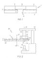
- FIG. 1 illustrates a polishing pad having a window of the present invention; and
- FIG. 2 illustrates a CMP system utilizing the polishing pad of the present invention.
- Referring now to Fig.1, a
polishing pad 1 of the present invention is shown.Polishing pad 1 comprises abottom layer 2 and atop layer 4. Thebottom layer 2 may be made of a felted polyurethane, such as SUBA-IV™ manufactured by Rodel, Inc. of Newark, DE. Thetop layer 4 may comprise a polyurethane pad (e.g., a pad filled with microspheres), such as, IC 1000™ by Rodel. A thin layer of pressuresensitive adhesive 6 holds thetop layer 4 and thebottom layer 2 together. - In an exemplary embodiment, an intact bottom layer 2 (i.e., without an aperture formed within the layer 2) has its top surface coated with the pressure
sensitive adhesive 6. An intact top layer 44 is then provided over thebottom layer 2 and on the pressuresensitive adhesive 6. Alternatively, thetop layer 4 may already include anaperture 8 prior to thetop layer 4 being being joined with the pressuresensitive adhesive 6. Next, anaperture 10 is formed in thebottom layer 2. Formation of thisaperture 10 removes the pressuresensitive adhesive 6 within theaperture 10 so that an open channel exists through thepolishing pad 1. Theaperture 8 in thetop layer 4 is wider than theaperture 10 in thebottom layer 2. This creates ashelf 12 covered with pressuresensitive adhesive 6. Thereafter, atransparent window block 14, is disposed over the pressuresensitive adhesive 6 on theshelf 12. Thetransparent window block 14 completely fills theaperture 8 in thetop layer 4. Accordingly, laser light from a laser spectrophotometer (not shown) may be directed through theaperture 10 andtransparent window block 14, and onto a wafer or substrate to facilitate end-point detection. - In an exemplary embodiment of the present invention,
window 14 is made from an aliphatic polyisocyanate-containing material ("prepolymer"). The prepolymer is a reaction product of an aliphatic polyisocyanate (e.g., diisocyanate) and a hydroxyl-containing material. The prepolymer is then cured with a curing agent. Preferred aliphatic polyisocyanates include, but are not limited to, methlene bis 4,4' cyclohexylisocyanate, cyclohexyl diisocyanate, isophorone diisocyanate, hexamethylene diisocyanate, propylene-1,2-diisocyanate, tetramethylene-1,4-diisocyanate, 1,6-hexamethylene-diisocyanate, dodecane-1,12-diisocyanate, cyclobutane-1,3-diisocyanate, cyclohexane-1,3-diisocyanate, cyclohexane-1,4- diisocyanate, 1-isocyanato-3,3,5-trimethyl-5-isocyanatomethylcyclohexane, methyl cyclohexylene diisocyanate, triisocyanate of hexamethylene diisocyanate, triisocyanate of 2,4,4-trimethyl-1,6-hexane diisocyanate, uretdione of hexamethylene diisocyanate, ethylene diisocyanate, 2,2,4-trimethylhexamethylene diisocyanate, 2,4,4-trimethylhexamethylene diisocyanate, dicyclohexylmethane diisocyanate, and mixtures thereof. The preferred aliphatic polyisocyanate has less than 14% unreacted isocyanate groups. - Advantageously, the hydroxyl-containing material is polyol. Exemplary polyols include, but are not limited to, polyether polyols, hydroxy-terminated polybutadiene (including partially/fully hydrogenated derivatives), polyester polyols, polycaprolactone polyols, and polycarbonate polyols.
- In one preferred embodiment, the polyol includes polyether polyol. Examples include, but are not limited to, polytetramethylene ether glycol ("PTMEG"), polyethylene propylene glycol, polyoxypropylene glycol, and mixtures thereof. The hydrocarbon chain can have saturated or unsaturated bonds and substituted or unsubstituted aromatic and cyclic groups. Preferably, the polyol of the present invention includes PTMEG. Suitable polyester polyols include, but are not limited to, polyethylene adipate glycol, polybutylene adipate glycol, polyethylene propylene adipate glycol, o-phthalate-1,6-hexanediol, poly(hexamethylene adipate) glycol, and mixtures thereof. The hydrocarbon chain can have saturated or unsaturated bonds, or substituted or unsubstituted aromatic and cyclic groups. Suitable polycaprolactone polyols include, but are not limited to, 1,6-hexanediol-initiated polycaprolactone, diethylene glycol initiated polycaprolactone, trimethylol propane initiated polycaprolactone, neopentyl glycol initiated polycaprolactone, 1,4-butanediol-initiated polycaprolactone, PTMEG-initiated polycaprolactone, and mixtures thereof. The hydrocarbon chain can have saturated or unsaturated bonds, or substituted or unsubstituted aromatic and cyclic groups. Suitable polycarbonates include, but are not limited to, polyphthalate carbonate and poly(hexamethylene carbonate) glycol. The hydrocarbon chain can have saturated or unsaturated bonds, or substituted or unsubstituted aromatic and cyclic groups.
- Advantageously, the curing agent is a polydiamine. Preferred polydiamines include, but are not limited to, diethyl toluene diamine ("DETDA"), 3,5-dimethylthio-2,4-toluenediamine and isomers thereof, 3,5-diethyltoluene-2,4-diamine and isomers thereof, such as 3,5-diethyltoluene-2,6-diamine, 4,4'-bis-(sec-butylamino)-diphenylmethane, 1,4-bis-(sec-butylamino)-benzene, 4,4'-methylene-bis-(2-chloroaniline), 4,4'-methylene-bis-(3-chloro-2,6-diethylaniline) ("MCDEA"), polytetramethyleneoxide-di-p-aminobenzoate, N,N'-dialkyldiamino diphenyl methane, p,p'-methylene dianiline ("MDA"), m-phenylenediamine ("MPDA"), methylene-bis 2-chloroaniline ("MBOCA"), 4,4'-methylene-bis-(2-chloroaniline) ("MOCA"), 4,4'-methylene-bis-(2,6-diethylaniline) ("MDEA"), 4,4'-methylene-bis-(2,3-dichloroaniline) ("MDCA"), 4,4'-diamino-3,3'-diethyl-5,5'-dimethyl diphenylmethane, 2,2',3,3'-tetrachloro diamino diphenylmethane, trimethylene glycol di-p-aminobenzoate, and mixtures thereof. Preferably, the curing agent of the present invention includes 3,5-dimethylthio-2,4-toluenediamine and isomers thereof. Suitable polyamine curatives include both primary and secondary amines.
- In addition, other curatives such as, a diol, triol, tetraol, or hydroxy-terminated curative may be added to the aforementioned polyurethane composition. Suitable diol, triol, and tetraol groups include ethylene glycol, diethylene glycol, polyethylene glycol, propylene glycol, polypropylene glycol, lower molecular weight polytetramethylene ether glycol, 1,3-bis(2-hydroxyethoxy) benzene, 1,3-bis-[2-(2-hydroxyethoxy) ethoxy]benzene, 1,3-bis-{2-[2-(2-hydroxyethoxy) ethoxy]ethoxy}benzene, 1,4-butanediol, 1,5-pentanediol, 1,6-hexanediol, resorcinol-di-(beta-hydroxyethyl) ether, hydroquinone-di-(beta-hydroxyethyl) ether, and mixtures thereof. Preferred hydroxy-terminated curatives include 1,3-bis(2-hydroxyethoxy) benzene, 1,3-bis-[2-(2-hydroxyethoxy) ethoxy]benzene, 1,3-bis-{2-[2-(2-hydroxyethoxy) ethoxy]ethoxy}benzene, 1,4-butanediol, and mixtures thereof. Both the hydroxy-terminated and amine curatives can include one or more saturated, unsaturated, aromatic, and cyclic groups. Additionally, the hydroxy-terminated and amine curatives can include one or more halogen groups. The polyurethane composition can be formed with a blend or mixture of curing agents. If desired, however, the polyurethane composition may be formed with a single curing agent.
- Accordingly, the present invention provides a chemical mechanical polishing pad comprising a window formed therein, wherein the window is formed from an aliphatic polyisocyanate-containing material. In particular, the window is formed from a reaction of an aliphatic polyisocyanate, a hydroxyl-containing material and a curing agent. The window of the present invention shows unexpected, improved transmission of laser signals for end-point detection during chemical mechanical polishing.
- Referring now to FIG. 2, a
CMP apparatus 20 utilizing the polishing pad of the present invention is provided.Apparatus 20 includes awafer carrier 22 for holding or pressing thesemiconductor wafer 24 against the polishingplaten 26. The polishingplaten 26 is provided withpad 1, includingwindow 14, of the present invention. As discussed above,pad 1 has abottom layer 2 that interfaces with the surface of the platen, and atop layer 4 that is used in conjunction with a chemical polishing slurry to polish thewafer 24. Note, although not pictured, any means for providing a polishing fluid or slurry can be utilized with the present apparatus. Theplaten 26 is usually rotated about itscentral axis 27. In addition, thewafer carrier 22 is usually rotated about itscentral axis 28, and translated across the surface of theplaten 26 via atranslation arm 30. Note, although a single wafer carrier is shown in FIG. 2, CMP apparatuses may have more than one spaced circumferentially around the polishing platen. In addition, ahole 32 is provided in theplaten 26 and overlies thewindow 14 ofpad 1. Accordingly,hole 32 provides access to the surface of thewafer 24, viawindow 14, during polishing of thewafer 24 for accurate end-point detection. Namely, alaser spectrophotometer 34 is provided below theplaten 26 which projects alaser beam 36 to pass and return through thehole 32 andhigh transmission window 14 for accurate end-point detection during polishing of thewafer 24. - In the Examples, numerals represent examples of the invention and the letter represents a comparative example. In this experiment, the percent optical transmission for exemplary windows of the present invention was measured using a Gretag Macbeth 3000A spectrophotometer, for the wavelength range of 360 nm to 750 nm. In particular, windows formed from aliphatic diisocyanate-containing materials were tested against a window formed from an aromatic diisocyanate-containing material. For Test A, 100 parts of the prepolymer kept at 120°F, with 26 parts of the curing agent kept at 240°F, was mixed in a liquid tank and degassed under vacuum (<1 torr). The mixture was then cast in a mold and cured at 220°F for 18 hours. For Tests 1-8, 100 parts of the prepolymer kept at 150°F, with appropriate amounts of the curing agent kept at room temperature, was mixed in a liquid tank and degassed under vacuum (<1 torr). The mixture was then cast in a mold and cured at 220°F for 18 hours. Adiprene® LW520 and LW570 are registered trademarks of Uniroyal Chemical, Inc. and are commercially available aliphatic diisocyanate-containing prepolymers. The LW520 has an NCO of 4.6 to 4.9 wt% and LW570 has an NCO of 7.35 to 7.65 wt %. Adiprene® L325 is a registered trademark of Uniroyal Chemical, Inc. and is a commercially available aromatic diisocyanate-containing prepolymer. The L325 has an NCO of 8.95 to 9.25 wt%.
Test Prepolymer (100 parts by weight) Curing agent (parts by weight) Trans 360 nm (%) Trans 400 nm (%) Trans 450 nm (%) Trans 550 nm (%) Trans 650 nm (%) Trans 750 nm (%) A Adiprene L325 MBOCA (26) 1 13 57 74 79 82 1 Adiprene LW520 DETDA (9.6) 89 93 93 94 93 93 2 Adiprene LW570 DETDA (15.1) 90 95 95 95 95 95 3 Adiprene 75%LW570/25%LW520 DETDA (13.8) 87 93 94 94 94 94 4 Adiprene LW520 MCDEA (20) 84 92 94 95 95 95 5 Adiprene LW570 MCDEA (31.7) 59 87 94 94 94 94 6 Adiprene LW520 MBOCA (14.3) 10 55 87 92 94 94 7 Adiprene 75%LW570/25%LW520 MBOCA (20.6) 5 45 87 94 94 94 8 Adiprene LW570 MBOCA (22.6) 1 21 69 85 90 92 - As illustrated in Table 1 above, all of the windows made from an aliphatic diisocyanate-containing material provided an overall improved percent transmission over the wavelength range of 360 nm to 750 nm.
Test 2 showed at least 90% transmission of the end-point signal over the entire wavelength range of 360 nm to 750 nm.Tests - In addition, as shown in Table 1, the aliphatic diisocyanates typically achieves the desired hardness and transmission values, at lower levels of curative content, minimizing the detrimental effects of curatives as discussed above. For example, in Tests 1-4 and 6-8, the amount of curing agent to achieve the desired hardness was less than that required for Test A, which required 26 parts of the curing agent to achieve the same level of hardness.
- Accordingly, the present invention provides a chemical mechanical polishing pad comprising a window formed therein, wherein the window is formed from an aliphatic polyisocyanate-containing material. In particular, the window is formed from a reaction of an aliphatic polyisocyanate, a hydroxyl-containing material and a curing agent. The window of the present invention allows for an optical signal strength (e.g., the relative intensity of beam as it exits/enters the window) greater than otherwise possible with prior art windows having less optical transmission over the wavelength range of in-situ optical endpoint detection or measurement systems. These improvements in signal strength lead to significant improvements in the in-situ optical measurement of wafer surface parameters. In particular, reliability and measurement accuracy for end-point detection are improved.
Claims (10)
- A chemical mechanical polishing pad comprising:wherein the window is formed from a reaction of an aliphatic polyisocyanate, a hydroxyl-containing material and a curing agent.a polishing pad having a window for end-point detection formed therein; and
- The polishing pad of claim 1 wherein the aliphatic diisocyanate is selected from the group comprising: methlene bis 4,4' cyclohexylisocyanate, cyclohexyl diisocyanate, isophorone diisocyanate, hexamethylene diisocyanate, propylene-1,2-diisocyanate, tetramethylene-1,4-diisocyanate, 1,6-hexamethylene-diisocyanate, dodecane-1,12-diisocyanate, cyclobutane-1,3-diisocyanate, cyclohexane-1,3-diisocyanate, cyclohexane-1,4-diisocyanate, 1-isocyanato-3,3,5-trimethyl-5-isocyanatomethylcyclohexane, methyl cyclohexylene diisocyanate, triisocyanate of hexamethylene diisocyanate, triisocyanate of 2,4,4-trimethyl-1,6-hexane diisocyanate, uretdione of hexamethylene diisocyanate, ethylene diisocyanate, 2,2,4-trimethylhexamethylene diisocyanate, 2,4,4-trime thylhexamethylene diisocyanate, dicyclohexylmethane diisocyanate, and mixtures thereof.
- The polishing pad of claim 1 wherein the hydroxyl-containing group is selected from the group comprising: polyether polyols, hydroxy-terminated polybutadiene, polyester polyols, polycaprolactone polyols, polycarbonate polyols, and mixtures thereof.
- The polishing pad of claim 1 wherein the curing agent is selected from the group comprising: polydiamine, diol, triol, tetraol, and mixtures thereof.
- The polishing pad of claim 1 wherein the aliphatic polyisocyanate has less than 14% unreacted isocyante groups.
- The polishing pad of claim 1 wherein the window has an optical transmission of at least 21% over a wavelength range of 400-750 nm.
- An apparatus for chemical mechanical polishing comprising:wherein the window is formed by reacting an aliphatic polyisocyanate, a hydroxyl-containing material and a curing agent.a platen for supporting a polishing pad, the polishing pad having a window for end-point detection formed therein;a wafer carrier for pressing a wafer against the polishing pad;means for providing a polishing fluid between the wafer and the polishing pad; and
- A method of forming a chemical mechanical polishing pad, the method comprising:wherein the window is formed by reacting an aliphatic polyisocyanate, a hydroxyl-containing material and a curing agent.providing a polishing pad having a window for end-point detection formed therein; and
- The method of claim 8 wherein the aliphatic polyisocyanate is selected from the group comprising: methlene bis 4, 4 cyclohexylisocyanate, cyclohexyl diisocyanate, isophorone diisocyanate, hexamethylene diisocyanate, propylene-1,2-diisocyanate, tetramethylene-1,4-diisocyanate, 1,6-hexamethylene-diisocyanate, dodecane-1,12-diisocyanate, cyclobutane-1,3-diisocyanate, cyclohexane-1,3-diisocyanate, cyclohexane-1,4- diisocyanate, 1-isocyanato-3,3,5-trimethyl-5-isocyanatomethylcyclohexane, methyl cyclohexylene diisocyanate, triisocyanate of hexamethylene diisocyanate, triisocyanate of 2,4,4-trimethyl-1,6-hexane diisocyanate, uretdione of hexamethylene diisocyanate, ethylene diisocyanate, 2,2,4-trimethylhexamethylene diisocyanate, 2,4,4-trimethylhexamethylene diisocyanate, dicyclohexylmethane diisocyanate, and mixtures thereof.
- The method of claim 8 wherein the window has an optical transmission of at least 21% over a wavelength range of 400-750 nm.
Applications Claiming Priority (2)
| Application Number | Priority Date | Filing Date | Title |
|---|---|---|---|
| US722739 | 1991-06-27 | ||
| US10/722,739 US6984163B2 (en) | 2003-11-25 | 2003-11-25 | Polishing pad with high optical transmission window |
Publications (2)
| Publication Number | Publication Date |
|---|---|
| EP1535699A1 true EP1535699A1 (en) | 2005-06-01 |
| EP1535699B1 EP1535699B1 (en) | 2006-05-03 |
Family
ID=34465692
Family Applications (1)
| Application Number | Title | Priority Date | Filing Date |
|---|---|---|---|
| EP04257057A Active EP1535699B1 (en) | 2003-11-25 | 2004-11-15 | Polishing pad with high optical transmission window |
Country Status (7)
| Country | Link |
|---|---|
| US (1) | US6984163B2 (en) |
| EP (1) | EP1535699B1 (en) |
| JP (1) | JP2005175464A (en) |
| KR (1) | KR101120647B1 (en) |
| CN (1) | CN100347826C (en) |
| DE (1) | DE602004000805T2 (en) |
| TW (1) | TWI324545B (en) |
Cited By (1)
| Publication number | Priority date | Publication date | Assignee | Title |
|---|---|---|---|---|
| US9999955B2 (en) | 2013-07-11 | 2018-06-19 | Ebara Corporation | Polishing apparatus and polished-state monitoring method |
Families Citing this family (69)
| Publication number | Priority date | Publication date | Assignee | Title |
|---|---|---|---|---|
| US20040209066A1 (en) * | 2003-04-17 | 2004-10-21 | Swisher Robert G. | Polishing pad with window for planarization |
| US7204742B2 (en) * | 2004-03-25 | 2007-04-17 | Cabot Microelectronics Corporation | Polishing pad comprising hydrophobic region and endpoint detection port |
| US7018581B2 (en) * | 2004-06-10 | 2006-03-28 | Rohm And Haas Electronic Materials Cmp Holdings, Inc. | Method of forming a polishing pad with reduced stress window |
| US20060089095A1 (en) * | 2004-10-27 | 2006-04-27 | Swisher Robert G | Polyurethane urea polishing pad |
| US20060089093A1 (en) * | 2004-10-27 | 2006-04-27 | Swisher Robert G | Polyurethane urea polishing pad |
| US20060089094A1 (en) * | 2004-10-27 | 2006-04-27 | Swisher Robert G | Polyurethane urea polishing pad |
| US7275928B2 (en) * | 2004-11-23 | 2007-10-02 | Rohm And Haas Electronic Materials Cmp Holdings, Inc. | Apparatus for forming a striation reduced chemical mechanical polishing pad |
| US20060108701A1 (en) * | 2004-11-23 | 2006-05-25 | Saikin Allan H | Method for forming a striation reduced chemical mechanical polishing pad |
| TWI410314B (en) * | 2005-04-06 | 2013-10-01 | 羅門哈斯電子材料Cmp控股公司 | Apparatus for forming a porous reaction injection molded chemical mechanical polishing pad |
| US7179151B1 (en) * | 2006-03-27 | 2007-02-20 | Freescale Semiconductor, Inc. | Polishing pad, a polishing apparatus, and a process for using the polishing pad |
| JP2007307639A (en) * | 2006-05-17 | 2007-11-29 | Toyo Tire & Rubber Co Ltd | Polishing pad |
| JP5110677B2 (en) * | 2006-05-17 | 2012-12-26 | 東洋ゴム工業株式会社 | Polishing pad |
| EP1894900A3 (en) * | 2006-08-28 | 2010-02-24 | Osaka University | Catalyst-aided chemical processing method and apparatus |
| JP4971028B2 (en) * | 2007-05-16 | 2012-07-11 | 東洋ゴム工業株式会社 | Polishing pad manufacturing method |
| US20090062414A1 (en) * | 2007-08-28 | 2009-03-05 | David Picheng Huang | System and method for producing damping polyurethane CMP pads |
| US8052507B2 (en) * | 2007-11-20 | 2011-11-08 | Praxair Technology, Inc. | Damping polyurethane CMP pads with microfillers |
| EP2227350A4 (en) * | 2007-11-30 | 2011-01-12 | Innopad Inc | Chemical-mechanical planarization pad having end point detection window |
| US8083570B2 (en) * | 2008-10-17 | 2011-12-27 | Rohm And Haas Electronic Materials Cmp Holdings, Inc. | Chemical mechanical polishing pad having sealed window |
| US8257544B2 (en) | 2009-06-10 | 2012-09-04 | Rohm And Haas Electronic Materials Cmp Holdings, Inc. | Chemical mechanical polishing pad having a low defect integral window |
| TWI396602B (en) * | 2009-12-31 | 2013-05-21 | Iv Technologies Co Ltd | Method of manufacturing polishing pad having detection window and polishing pad having detection window |
| US9017140B2 (en) | 2010-01-13 | 2015-04-28 | Nexplanar Corporation | CMP pad with local area transparency |
| US8697217B2 (en) | 2010-01-15 | 2014-04-15 | Rohm and Haas Electronics Materials CMP Holdings, Inc. | Creep-resistant polishing pad window |
| CN102133734B (en) * | 2010-01-21 | 2015-02-04 | 智胜科技股份有限公司 | Grinding pad with detecting window and manufacturing method thereof |
| TWI510526B (en) * | 2010-06-25 | 2015-12-01 | 羅門哈斯電子材料Cmp控股公司 | A chemical mechanical polishing pad having a low defect integral window |
| US9156124B2 (en) | 2010-07-08 | 2015-10-13 | Nexplanar Corporation | Soft polishing pad for polishing a semiconductor substrate |
| CN102310366B (en) * | 2010-07-08 | 2014-03-05 | 罗门哈斯电子材料Cmp控股股份有限公司 | Chemical mechanical polishing pad with low-defect overall window |
| US8257545B2 (en) | 2010-09-29 | 2012-09-04 | Rohm And Haas Electronic Materials Cmp Holdings, Inc. | Chemical mechanical polishing pad with light stable polymeric endpoint detection window and method of polishing therewith |
| US8758659B2 (en) | 2010-09-29 | 2014-06-24 | Fns Tech Co., Ltd. | Method of grooving a chemical-mechanical planarization pad |
| JP5732354B2 (en) * | 2011-09-01 | 2015-06-10 | 東洋ゴム工業株式会社 | Polishing pad |
| US9156125B2 (en) * | 2012-04-11 | 2015-10-13 | Cabot Microelectronics Corporation | Polishing pad with light-stable light-transmitting region |
| US9186772B2 (en) | 2013-03-07 | 2015-11-17 | Rohm And Haas Electronic Materials Cmp Holdings, Inc. | Chemical mechanical polishing pad with broad spectrum, endpoint detection window and method of polishing therewith |
| US20140256231A1 (en) * | 2013-03-07 | 2014-09-11 | Dow Global Technologies Llc | Multilayer Chemical Mechanical Polishing Pad With Broad Spectrum, Endpoint Detection Window |
| US9446497B2 (en) | 2013-03-07 | 2016-09-20 | Rohm And Haas Electronic Materials Cmp Holdings, Inc. | Broad spectrum, endpoint detection monophase olefin copolymer window with specific composition in multilayer chemical mechanical polishing pad |
| US9238295B2 (en) * | 2013-05-31 | 2016-01-19 | Rohm And Haas Electronic Materials Cmp Holdings, Inc. | Soft and conditionable chemical mechanical window polishing pad |
| US9233451B2 (en) * | 2013-05-31 | 2016-01-12 | Rohm And Haas Electronic Materials Cmp Holdings, Inc. | Soft and conditionable chemical mechanical polishing pad stack |
| US9259820B2 (en) | 2014-03-28 | 2016-02-16 | Rohm And Haas Electronic Materials Cmp Holdings, Inc. | Chemical mechanical polishing pad with polishing layer and window |
| US9064806B1 (en) | 2014-03-28 | 2015-06-23 | Rohm and Haas Electronics Materials CMP Holdings, Inc. | Soft and conditionable chemical mechanical polishing pad with window |
| US9216489B2 (en) | 2014-03-28 | 2015-12-22 | Rohm And Haas Electronic Materials Cmp Holdings, Inc. | Chemical mechanical polishing pad with endpoint detection window |
| US9314897B2 (en) | 2014-04-29 | 2016-04-19 | Rohm And Haas Electronic Materials Cmp Holdings, Inc. | Chemical mechanical polishing pad with endpoint detection window |
| US9333620B2 (en) * | 2014-04-29 | 2016-05-10 | Rohm And Haas Electronic Materials Cmp Holdings, Inc. | Chemical mechanical polishing pad with clear endpoint detection window |
| US9873180B2 (en) | 2014-10-17 | 2018-01-23 | Applied Materials, Inc. | CMP pad construction with composite material properties using additive manufacturing processes |
| US11745302B2 (en) | 2014-10-17 | 2023-09-05 | Applied Materials, Inc. | Methods and precursor formulations for forming advanced polishing pads by use of an additive manufacturing process |
| US10821573B2 (en) | 2014-10-17 | 2020-11-03 | Applied Materials, Inc. | Polishing pads produced by an additive manufacturing process |
| US10875145B2 (en) | 2014-10-17 | 2020-12-29 | Applied Materials, Inc. | Polishing pads produced by an additive manufacturing process |
| CN107078048B (en) | 2014-10-17 | 2021-08-13 | 应用材料公司 | CMP pad construction with composite material properties using additive manufacturing process |
| US10399201B2 (en) | 2014-10-17 | 2019-09-03 | Applied Materials, Inc. | Advanced polishing pads having compositional gradients by use of an additive manufacturing process |
| US10875153B2 (en) | 2014-10-17 | 2020-12-29 | Applied Materials, Inc. | Advanced polishing pad materials and formulations |
| US9586304B2 (en) * | 2014-12-19 | 2017-03-07 | Rohm And Haas Electronic Materials Cmp Holdings, Inc. | Controlled-expansion CMP PAD casting method |
| US9475168B2 (en) | 2015-03-26 | 2016-10-25 | Rohm And Haas Electronic Materials Cmp Holdings, Inc. | Polishing pad window |
| CN113103145B (en) | 2015-10-30 | 2023-04-11 | 应用材料公司 | Apparatus and method for forming polishing article having desired zeta potential |
| US9868185B2 (en) * | 2015-11-03 | 2018-01-16 | Cabot Microelectronics Corporation | Polishing pad with foundation layer and window attached thereto |
| US10391605B2 (en) | 2016-01-19 | 2019-08-27 | Applied Materials, Inc. | Method and apparatus for forming porous advanced polishing pads using an additive manufacturing process |
| KR101904322B1 (en) * | 2017-01-23 | 2018-10-04 | 에스케이씨 주식회사 | Polishing pad and preparation method thereof |
| KR101889081B1 (en) * | 2017-03-16 | 2018-08-16 | 에스케이씨 주식회사 | Polishing pad and preparation method thereof |
| US10293456B2 (en) * | 2017-04-19 | 2019-05-21 | Rohm And Haas Electronic Materials Cmp Holdings, Inc. | Aliphatic polyurethane optical endpoint detection windows and CMP polishing pads containing them |
| US10207388B2 (en) * | 2017-04-19 | 2019-02-19 | Rohm And Haas Electronic Materials Cmp Holdings, Inc. | Aliphatic polyurethane optical endpoint detection windows and CMP polishing pads containing them |
| US10596763B2 (en) | 2017-04-21 | 2020-03-24 | Applied Materials, Inc. | Additive manufacturing with array of energy sources |
| US10391606B2 (en) * | 2017-06-06 | 2019-08-27 | Rohm And Haas Electronic Materials Cmp Holdings, Inc. | Chemical mechanical polishing pads for improved removal rate and planarization |
| US11471999B2 (en) | 2017-07-26 | 2022-10-18 | Applied Materials, Inc. | Integrated abrasive polishing pads and manufacturing methods |
| US11072050B2 (en) | 2017-08-04 | 2021-07-27 | Applied Materials, Inc. | Polishing pad with window and manufacturing methods thereof |
| WO2019032286A1 (en) | 2017-08-07 | 2019-02-14 | Applied Materials, Inc. | Abrasive delivery polishing pads and manufacturing methods thereof |
| US10465097B2 (en) * | 2017-11-16 | 2019-11-05 | Rohm And Haas Electronic Materials Cmp Holdings, Inc. | Aliphatic UV cured polyurethane optical endpoint detection windows with high UV transparency for CMP polishing pads |
| CN112654655A (en) | 2018-09-04 | 2021-04-13 | 应用材料公司 | Advanced polishing pad formulations |
| US11813712B2 (en) | 2019-12-20 | 2023-11-14 | Applied Materials, Inc. | Polishing pads having selectively arranged porosity |
| US11806829B2 (en) | 2020-06-19 | 2023-11-07 | Applied Materials, Inc. | Advanced polishing pads and related polishing pad manufacturing methods |
| KR102421208B1 (en) * | 2020-09-10 | 2022-07-14 | 에스케이씨솔믹스 주식회사 | Polishing pad and preparing method of semiconductor device using the same |
| US11878389B2 (en) | 2021-02-10 | 2024-01-23 | Applied Materials, Inc. | Structures formed using an additive manufacturing process for regenerating surface texture in situ |
| KR102623920B1 (en) * | 2021-07-27 | 2024-01-10 | 에스케이엔펄스 주식회사 | Polishing pad and preparing method of semiconductor device using the same |
| KR20230112387A (en) * | 2022-01-20 | 2023-07-27 | 케이피엑스케미칼 주식회사 | Method for manufacturing a window for polishing pad and window for polishing pad manufactured by the same |
Citations (1)
| Publication number | Priority date | Publication date | Assignee | Title |
|---|---|---|---|---|
| US6280290B1 (en) * | 1995-03-28 | 2001-08-28 | Applied Materials, Inc. | Method of forming a transparent window in a polishing pad |
Family Cites Families (17)
| Publication number | Priority date | Publication date | Assignee | Title |
|---|---|---|---|---|
| US3866242A (en) * | 1972-10-27 | 1975-02-18 | Goodyear Aerospace Corp | Protective shield |
| US5605760A (en) * | 1995-08-21 | 1997-02-25 | Rodel, Inc. | Polishing pads |
| US6832950B2 (en) * | 2002-10-28 | 2004-12-21 | Applied Materials, Inc. | Polishing pad with window |
| US6171181B1 (en) * | 1999-08-17 | 2001-01-09 | Rodel Holdings, Inc. | Molded polishing pad having integral window |
| JP3506114B2 (en) * | 2000-01-25 | 2004-03-15 | 株式会社ニコン | MONITOR DEVICE, POLISHING APPARATUS HAVING THE MONITOR DEVICE, AND POLISHING METHOD |
| KR20020084150A (en) * | 2000-02-25 | 2002-11-04 | 로델 홀딩스 인코포레이티드 | Polishing pad with a transparent portion |
| JP2002001647A (en) * | 2000-06-19 | 2002-01-08 | Rodel Nitta Co | Polishing pad |
| JP3756098B2 (en) | 2000-10-13 | 2006-03-15 | タレックス光学工業株式会社 | Polyurethane resin material composition for casting and impact-resistant optical lens |
| JP2003048151A (en) * | 2001-08-08 | 2003-02-18 | Rodel Nitta Co | Polishing pad |
| JP2003285258A (en) * | 2002-03-28 | 2003-10-07 | Toray Ind Inc | Polishing pad, polishing apparatus, and method for manufacturing semiconductor device |
| JP2003285259A (en) * | 2002-03-28 | 2003-10-07 | Toray Ind Inc | Polishing pad, polishing apparatus, and method for manufacturing semiconductor device |
| WO2004028744A1 (en) * | 2002-09-25 | 2004-04-08 | Ppg Industries Ohio, Inc. | Polishing pad with window for planarization |
| US7435165B2 (en) * | 2002-10-28 | 2008-10-14 | Cabot Microelectronics Corporation | Transparent microporous materials for CMP |
| JP4849587B2 (en) * | 2003-03-11 | 2012-01-11 | 東洋ゴム工業株式会社 | Polishing pad and method for manufacturing semiconductor device |
| JP2004319584A (en) * | 2003-04-11 | 2004-11-11 | Nihon Micro Coating Co Ltd | Polishing pad and its manufacturing method |
| US20040209066A1 (en) * | 2003-04-17 | 2004-10-21 | Swisher Robert G. | Polishing pad with window for planarization |
| US7195539B2 (en) * | 2003-09-19 | 2007-03-27 | Cabot Microelectronics Coporation | Polishing pad with recessed window |
-
2003
- 2003-11-25 US US10/722,739 patent/US6984163B2/en not_active Expired - Lifetime
-
2004
- 2004-11-10 TW TW093134352A patent/TWI324545B/en not_active IP Right Cessation
- 2004-11-15 DE DE602004000805T patent/DE602004000805T2/en active Active
- 2004-11-15 EP EP04257057A patent/EP1535699B1/en active Active
- 2004-11-24 CN CNB2004100950388A patent/CN100347826C/en not_active Ceased
- 2004-11-25 KR KR1020040097316A patent/KR101120647B1/en active IP Right Grant
- 2004-11-25 JP JP2004339942A patent/JP2005175464A/en active Pending
Patent Citations (1)
| Publication number | Priority date | Publication date | Assignee | Title |
|---|---|---|---|---|
| US6280290B1 (en) * | 1995-03-28 | 2001-08-28 | Applied Materials, Inc. | Method of forming a transparent window in a polishing pad |
Cited By (1)
| Publication number | Priority date | Publication date | Assignee | Title |
|---|---|---|---|---|
| US9999955B2 (en) | 2013-07-11 | 2018-06-19 | Ebara Corporation | Polishing apparatus and polished-state monitoring method |
Also Published As
| Publication number | Publication date |
|---|---|
| US6984163B2 (en) | 2006-01-10 |
| KR101120647B1 (en) | 2012-03-16 |
| JP2005175464A (en) | 2005-06-30 |
| TW200531785A (en) | 2005-10-01 |
| EP1535699B1 (en) | 2006-05-03 |
| DE602004000805T2 (en) | 2006-11-30 |
| CN100347826C (en) | 2007-11-07 |
| US20050113008A1 (en) | 2005-05-26 |
| TWI324545B (en) | 2010-05-11 |
| CN1622289A (en) | 2005-06-01 |
| DE602004000805D1 (en) | 2006-06-08 |
| KR20050050582A (en) | 2005-05-31 |
Similar Documents
| Publication | Publication Date | Title |
|---|---|---|
| US6984163B2 (en) | Polishing pad with high optical transmission window | |
| US7018581B2 (en) | Method of forming a polishing pad with reduced stress window | |
| JP4761846B2 (en) | Polishing pad with pressure relief passage | |
| US8257545B2 (en) | Chemical mechanical polishing pad with light stable polymeric endpoint detection window and method of polishing therewith | |
| US9259820B2 (en) | Chemical mechanical polishing pad with polishing layer and window | |
| US9102034B2 (en) | Method of chemical mechanical polishing a substrate | |
| KR102411323B1 (en) | Soft and conditionable chemical mechanical polishing pad with window | |
| TWI590919B (en) | Soft and conditionable chemical mechanical polishing pad with window and method of polishing substrate | |
| US20100317261A1 (en) | Chemical mechanical polishing pad having a low defect integral window | |
| US20150065013A1 (en) | Chemical mechanical polishing pad | |
| KR101911083B1 (en) | Creep-resistant polishing pad window | |
| KR102590761B1 (en) | Chemical mechanical polishing pad | |
| KR101092944B1 (en) | polishing pad | |
| KR20150112855A (en) | Chemical mechanical polishing pad with endpoint detection window | |
| KR102085640B1 (en) | Method of manufacturing grooved chemical mechanical polishing layers | |
| JP2023050503A (en) | Manufacturing method of window material for endpoint detection | |
| KR20230112387A (en) | Method for manufacturing a window for polishing pad and window for polishing pad manufactured by the same |
Legal Events
| Date | Code | Title | Description |
|---|---|---|---|
| PUAI | Public reference made under article 153(3) epc to a published international application that has entered the european phase |
Free format text: ORIGINAL CODE: 0009012 |
|
| 17P | Request for examination filed |
Effective date: 20041125 |
|
| AK | Designated contracting states |
Kind code of ref document: A1 Designated state(s): AT BE BG CH CY CZ DE DK EE ES FI FR GB GR HU IE IS IT LI LU MC NL PL PT RO SE SI SK TR |
|
| AX | Request for extension of the european patent |
Extension state: AL HR LT LV MK YU |
|
| GRAP | Despatch of communication of intention to grant a patent |
Free format text: ORIGINAL CODE: EPIDOSNIGR1 |
|
| AKX | Designation fees paid |
Designated state(s): DE FR GB IT |
|
| GRAS | Grant fee paid |
Free format text: ORIGINAL CODE: EPIDOSNIGR3 |
|
| GRAA | (expected) grant |
Free format text: ORIGINAL CODE: 0009210 |
|
| AK | Designated contracting states |
Kind code of ref document: B1 Designated state(s): DE FR GB IT |
|
| PG25 | Lapsed in a contracting state [announced via postgrant information from national office to epo] |
Ref country code: IT Free format text: LAPSE BECAUSE OF FAILURE TO SUBMIT A TRANSLATION OF THE DESCRIPTION OR TO PAY THE FEE WITHIN THE PRESCRIBED TIME-LIMIT;WARNING: LAPSES OF ITALIAN PATENTS WITH EFFECTIVE DATE BEFORE 2007 MAY HAVE OCCURRED AT ANY TIME BEFORE 2007. THE CORRECT EFFECTIVE DATE MAY BE DIFFERENT FROM THE ONE RECORDED. Effective date: 20060503 |
|
| REG | Reference to a national code |
Ref country code: GB Ref legal event code: FG4D |
|
| REF | Corresponds to: |
Ref document number: 602004000805 Country of ref document: DE Date of ref document: 20060608 Kind code of ref document: P |
|
| ET | Fr: translation filed | ||
| PLBE | No opposition filed within time limit |
Free format text: ORIGINAL CODE: 0009261 |
|
| STAA | Information on the status of an ep patent application or granted ep patent |
Free format text: STATUS: NO OPPOSITION FILED WITHIN TIME LIMIT |
|
| 26N | No opposition filed |
Effective date: 20070206 |
|
| PGFP | Annual fee paid to national office [announced via postgrant information from national office to epo] |
Ref country code: IT Payment date: 20101120 Year of fee payment: 7 |
|
| PG25 | Lapsed in a contracting state [announced via postgrant information from national office to epo] |
Ref country code: IT Free format text: LAPSE BECAUSE OF NON-PAYMENT OF DUE FEES Effective date: 20121115 |
|
| REG | Reference to a national code |
Ref country code: FR Ref legal event code: PLFP Year of fee payment: 12 |
|
| REG | Reference to a national code |
Ref country code: FR Ref legal event code: PLFP Year of fee payment: 13 |
|
| REG | Reference to a national code |
Ref country code: FR Ref legal event code: PLFP Year of fee payment: 14 |
|
| REG | Reference to a national code |
Ref country code: FR Ref legal event code: PLFP Year of fee payment: 15 |
|
| PGFP | Annual fee paid to national office [announced via postgrant information from national office to epo] |
Ref country code: GB Payment date: 20220930 Year of fee payment: 19 |
|
| PGFP | Annual fee paid to national office [announced via postgrant information from national office to epo] |
Ref country code: FR Payment date: 20221010 Year of fee payment: 19 |
|
| PGFP | Annual fee paid to national office [announced via postgrant information from national office to epo] |
Ref country code: DE Payment date: 20220621 Year of fee payment: 19 |