EP1540657B1 - Software refreshed memory device and method - Google Patents
Software refreshed memory device and method Download PDFInfo
- Publication number
- EP1540657B1 EP1540657B1 EP03749204A EP03749204A EP1540657B1 EP 1540657 B1 EP1540657 B1 EP 1540657B1 EP 03749204 A EP03749204 A EP 03749204A EP 03749204 A EP03749204 A EP 03749204A EP 1540657 B1 EP1540657 B1 EP 1540657B1
- Authority
- EP
- European Patent Office
- Prior art keywords
- memory
- refreshed
- refresh
- cell
- given cell
- Prior art date
- Legal status (The legal status is an assumption and is not a legal conclusion. Google has not performed a legal analysis and makes no representation as to the accuracy of the status listed.)
- Expired - Lifetime
Links
Images


Classifications
-
- G—PHYSICS
- G11—INFORMATION STORAGE
- G11C—STATIC STORES
- G11C5/00—Details of stores covered by group G11C11/00
- G11C5/005—Circuit means for protection against loss of information of semiconductor storage devices
-
- G—PHYSICS
- G11—INFORMATION STORAGE
- G11C—STATIC STORES
- G11C11/00—Digital stores characterised by the use of particular electric or magnetic storage elements; Storage elements therefor
- G11C11/21—Digital stores characterised by the use of particular electric or magnetic storage elements; Storage elements therefor using electric elements
- G11C11/34—Digital stores characterised by the use of particular electric or magnetic storage elements; Storage elements therefor using electric elements using semiconductor devices
- G11C11/40—Digital stores characterised by the use of particular electric or magnetic storage elements; Storage elements therefor using electric elements using semiconductor devices using transistors
- G11C11/401—Digital stores characterised by the use of particular electric or magnetic storage elements; Storage elements therefor using electric elements using semiconductor devices using transistors forming cells needing refreshing or charge regeneration, i.e. dynamic cells
- G11C11/406—Management or control of the refreshing or charge-regeneration cycles
- G11C11/40603—Arbitration, priority and concurrent access to memory cells for read/write or refresh operations
-
- G—PHYSICS
- G11—INFORMATION STORAGE
- G11C—STATIC STORES
- G11C11/00—Digital stores characterised by the use of particular electric or magnetic storage elements; Storage elements therefor
- G11C11/21—Digital stores characterised by the use of particular electric or magnetic storage elements; Storage elements therefor using electric elements
- G11C11/34—Digital stores characterised by the use of particular electric or magnetic storage elements; Storage elements therefor using electric elements using semiconductor devices
- G11C11/40—Digital stores characterised by the use of particular electric or magnetic storage elements; Storage elements therefor using electric elements using semiconductor devices using transistors
- G11C11/401—Digital stores characterised by the use of particular electric or magnetic storage elements; Storage elements therefor using electric elements using semiconductor devices using transistors forming cells needing refreshing or charge regeneration, i.e. dynamic cells
- G11C11/406—Management or control of the refreshing or charge-regeneration cycles
- G11C11/40622—Partial refresh of memory arrays
-
- G—PHYSICS
- G11—INFORMATION STORAGE
- G11C—STATIC STORES
- G11C11/00—Digital stores characterised by the use of particular electric or magnetic storage elements; Storage elements therefor
- G11C11/21—Digital stores characterised by the use of particular electric or magnetic storage elements; Storage elements therefor using electric elements
- G11C11/34—Digital stores characterised by the use of particular electric or magnetic storage elements; Storage elements therefor using electric elements using semiconductor devices
- G11C11/40—Digital stores characterised by the use of particular electric or magnetic storage elements; Storage elements therefor using electric elements using semiconductor devices using transistors
- G11C11/401—Digital stores characterised by the use of particular electric or magnetic storage elements; Storage elements therefor using electric elements using semiconductor devices using transistors forming cells needing refreshing or charge regeneration, i.e. dynamic cells
- G11C11/4063—Auxiliary circuits, e.g. for addressing, decoding, driving, writing, sensing or timing
- G11C11/407—Auxiliary circuits, e.g. for addressing, decoding, driving, writing, sensing or timing for memory cells of the field-effect type
- G11C11/408—Address circuits
-
- G—PHYSICS
- G11—INFORMATION STORAGE
- G11C—STATIC STORES
- G11C13/00—Digital stores characterised by the use of storage elements not covered by groups G11C11/00, G11C23/00, or G11C25/00
- G11C13/0002—Digital stores characterised by the use of storage elements not covered by groups G11C11/00, G11C23/00, or G11C25/00 using resistive RAM [RRAM] elements
- G11C13/0004—Digital stores characterised by the use of storage elements not covered by groups G11C11/00, G11C23/00, or G11C25/00 using resistive RAM [RRAM] elements comprising amorphous/crystalline phase transition cells
-
- G—PHYSICS
- G11—INFORMATION STORAGE
- G11C—STATIC STORES
- G11C13/00—Digital stores characterised by the use of storage elements not covered by groups G11C11/00, G11C23/00, or G11C25/00
- G11C13/0002—Digital stores characterised by the use of storage elements not covered by groups G11C11/00, G11C23/00, or G11C25/00 using resistive RAM [RRAM] elements
- G11C13/0009—RRAM elements whose operation depends upon chemical change
- G11C13/0011—RRAM elements whose operation depends upon chemical change comprising conductive bridging RAM [CBRAM] or programming metallization cells [PMCs]
-
- G—PHYSICS
- G11—INFORMATION STORAGE
- G11C—STATIC STORES
- G11C13/00—Digital stores characterised by the use of storage elements not covered by groups G11C11/00, G11C23/00, or G11C25/00
- G11C13/0002—Digital stores characterised by the use of storage elements not covered by groups G11C11/00, G11C23/00, or G11C25/00 using resistive RAM [RRAM] elements
- G11C13/0021—Auxiliary circuits
- G11C13/0033—Disturbance prevention or evaluation; Refreshing of disturbed memory data
-
- G—PHYSICS
- G11—INFORMATION STORAGE
- G11C—STATIC STORES
- G11C13/00—Digital stores characterised by the use of storage elements not covered by groups G11C11/00, G11C23/00, or G11C25/00
- G11C13/0002—Digital stores characterised by the use of storage elements not covered by groups G11C11/00, G11C23/00, or G11C25/00 using resistive RAM [RRAM] elements
- G11C13/0021—Auxiliary circuits
- G11C13/0069—Writing or programming circuits or methods
-
- G—PHYSICS
- G11—INFORMATION STORAGE
- G11C—STATIC STORES
- G11C16/00—Erasable programmable read-only memories
- G11C16/02—Erasable programmable read-only memories electrically programmable
- G11C16/06—Auxiliary circuits, e.g. for writing into memory
- G11C16/34—Determination of programming status, e.g. threshold voltage, overprogramming or underprogramming, retention
- G11C16/3418—Disturbance prevention or evaluation; Refreshing of disturbed memory data
- G11C16/3431—Circuits or methods to detect disturbed nonvolatile memory cells, e.g. which still read as programmed but with threshold less than the program verify threshold or read as erased but with threshold greater than the erase verify threshold, and to reverse the disturbance via a refreshing programming or erasing step
Definitions
- This invention relates generally to computer memory devices and more particularly to memory devices that must be periodically refreshed to avoid losing data.
- Non-volatile memory devices can maintain the information stored in the memory indefinitely, even when the power to the memory device is turned off. These memory devices are known as non-volatile memory devices. Some examples of non-volatile memory devices include magnetic random access memories (MRAMs), erasable programmable read only memories (EPROMs), and variations thereof.
- MRAMs magnetic random access memories
- EPROMs erasable programmable read only memories
- DRAM dynamic random access memory
- Conventional volatile memory devices include a plurality of individual memory cells configured in an array, which typically comprises a configuration of intersecting rows and columns. To maintain the information stored in a conventional volatile memory device, each memory cell in the array is typically refreshed at least several times per second. For example, in some conventional DRAMs, each memory cell must be refreshed about once every 64 milliseconds to avoid losing the information stored in the DRAM. Accordingly, conventional volatile memory devices typically include refresh circuitry to ensure that every memory cell is refreshed at least as often as necessary to avoid losing data, which is commonly at least several times per second.
- US-5.574.684 describes a refresh method for a flash memory checking whether the threshold voltage of a cell is between two voltage limits (Program W and Erase W) and if this situation occurs, refreshing the cell by programming a zero ("0") by means of a write operation.
- a method of refreshing a cell is specified in claim 1.
- Figure 1 illustrates a computer system that includes a volatile memory device.
- Figure 2 illustrates a computer system having a software refreshed memory device in accordance with one embodiment of the present invention.
- Figure 3 illustrates a method of refreshing a memory cell in accordance with one embodiment of the present invention.
- Figure 4 illustrates a method of refreshing a plurality of memory cells in accordance with one embodiment of the present invention.
- Figure 5 illustrates a method of refreshing a plurality of memory cells in accordance with one embodiment of the present invention.
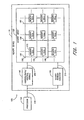
- Figure 1 illustrates a computer system 100 that includes a conventional volatile memory device 110.
- the computer system 100 also comprises a processor 120 coupled to the memory device 110 via a bus 130.
- the memory device 110 comprises an address/data/control module 140 and memory refresh circuitry 150, both of which are coupled to the processor 120 via the bus 130.
- the memory device 110 also comprises a memory array 160 coupled to the address/data/control module 140 via line 200 and to the memory refresh circuitry 150 via line 210.
- lines 200 and 210 may be implemented in the memory device 110 as part of a single physical bus.
- the memory array 160 comprises a plurality of memory cells 170; which are interconnected by a plurality of intersecting rows 180 and columns 190.
- the processor 120 transmits certain signals to the memory device 110 via the bus 130. For example, to read data stored at a particular memory address, the processor 120 issues a read command, together with the memory address, to the bus 130.
- the address/data/control module 140 receives and processes the read command by accessing the memory array 160 via line 200. Specifically, the address/data/control module 140 generates a read control signal on line 200 and addresses the desired memory cell 170 by activating the appropriate row 180 and column 190. The address/data/control module 140 then receives the data stored at the addressed memory cell 170 via line 200, and passes the data to the processor 120 via the bus 130.
- the processor 120 issues a write command, together with the memory address and the data to be stored, to the bus 130.
- the address/data/control module 140 receives and processes the write command by generating a write control signal on line 200 and addressing the desired memory cell 170, as described above.
- the address/data/control module 140 then passes the data to be stored to the addressed memory cell 170 via line 200.
- the primary function of the memory refresh circuitry 150 is to perform these periodic memory refresh operations.
- the memory refresh circuitry 150 determines that it is necessary to perform a memory refresh operation, the memory device 110 is made unavailable to the processor 120 to perform other operations, such as a read operation or a write operation.
- the memory refresh circuitry 150 To perform a memory refresh operation, the memory refresh circuitry 150 typically sequentially addresses the rows 180 of the memory array 160. When a given row 180 of the array 160 is addressed, the memory refresh circuitry generates a refresh control signal on line 210, which causes all of the memory cells 170 in the addressed row 180 to be refreshed simultaneously. By refreshing a large number of memory cells 170 simultaneously, the memory refresh circuitry 150 advantageously reduces the amount of time required to perform a memory refresh operation, thereby reducing the amount of time that the memory device 110 is unavailable to the processor 120 to perform other operations.
- the memory refresh circuitry 150 is often configured to identify time periods when the processor 120 is not likely to issue requests to the memory device 110, and to perform memory refresh operations during these identified time periods. On the other hand, because power is required to perform a memory refresh operation, it is desirable to minimize the number of memory refresh operations performed. Thus, the memory refresh circuitry 150 is also often configured to perform memory refresh operations as infrequently as possible, while preserving the data stored in the memory device 110.
- the memory refresh circuitry 150 must perform memory refresh operations frequently, often many times per second. For example, in some embodiments, each memory cell 170 must be refreshed at least about once every 64 milliseconds to avoid losing data. In these embodiments, to avoid losing the information stored in the memory device 110, the memory refresh circuitry 150 must ensure that every memory cell 170 is refreshed at least more often than about 15 times per second.
- FIG. 2 illustrates a computer system 250 having a software refreshed memory device 260 in accordance with one embodiment of the present invention.
- the computer system 250 also comprises a processor 270 coupled to the memory device 260 via a bus 280.
- the computer system 250 further comprises a set of memory refresh instructions 290, which are implemented in software that can be executed by the processor 270.
- the memory device 260 comprises an address/data/control module 300 which is coupled to the processor 270 via the bus 280.
- the memory device 260 also comprises a memory array 310 coupled to the address/data/control module 300 via line 350.
- the memory array 310 comprises a plurality of memory cells 320, which are interconnected by a plurality of intersecting rows 330 and columns 340.
- the computer system 250 illustrated in Figure 2 can perform memory read and write operations using the same methods described above in connection with Figure 1 . In addition to these methods, however, the computer system 250 can perform memory read and write operations in a variety of other ways that are well-known to those of ordinary skill in the art.
- the memory cells 320 of the software refreshed memory device 260 comprise volatile memory cells, which are preferably more stable than conventional DRAM memory cells.
- the memory cells 320 can avoid losing data even though the time interval between successive memory refresh operations is about 0.1 seconds.
- the time interval between successive memory refresh operations can be about one second.
- the time interval between successive memory refresh operations can be about one hour.
- the time interval between successive memory refresh operations can be about one day to one week.
- the memory cells 320 of the software refreshed memory device 260 comprise programmable conductor random access memory (PCRAM) cells, which are described in U.S. Patent Nos. 5,761,115 , 5,896,312 , 5,914,893 , 6,084,796 to Kozicki et al . ("the Kozicki patents"), in U.S. Patent No. 6,348,365 to Moore et al . (“the Moore patent”), and in the following U.S. patent Nos.
- PCRAM programmable conductor random access memory
- a PCRAM cell comprises a pair of electrodes and can exist in one of two possible states. In the first state, an electrical short exists between the electrodes of the PCRAM cell In the second state, an open circuit exists between the electrodes of the PCRAM cell.
- a PCRAM cell comprise a glass ion conductor, such as a chalcogenide-metal ion glass, and two electrodes disposed at the surface of the glass ion conductor and spaced a distance apart from one another.
- a PCRAM cell comprises germanium selenide with a Group IV metal (e.g., silver) dissolved therein, such as Ag/Gc 3 Se 7 .
- a Group IV metal e.g., silver
- one of the electrodes comprises a Group IV metal
- the glass element of the PCRAM cell contains the same metal.
- a conductive path is created between the electrodes along the sidewalls of the via in which the glass element is formed.
- a voltage having the opposite polarity is applied across the electrodes, the metal ions re-dissolve into the cell body, thereby causing the conductive path to disappear.
- the presence or absence of a conductive path within a PCRAM cell can be detected by measuring the electrical resistance between the electrodes.
- an electrical short exists between the electrodes, and the resistance between the electrodes is low ( e.g ., on the order of milliohms).
- no conductive path is present, an open circuit exists between the electrodes, and the resistance between the electrodes is high ( e.g ., on the order of megaohms).
- the memory cells 320 of the memory device 260 are capable of existing in one of two states, i.e ., a "written" state or an "erased” state.
- a memory cell 320 comprises a capacitor capable of holding a charge
- the presence of a charge in the capacitor would correspond to the written state
- the absence of a charge in the capacitor would correspond to the erased state.
- a PCRAM cell acts as a memory cell 320
- the presence of a conductive path between the electrodes would correspond to the written state
- the absence of a conductive path between the electrodes would correspond to the erased state.
- each memory cell 170 of a conventional volatile memory device 110 when a memory cell 170 of a conventional volatile memory device 110 is placed in a particular state, the memory cell 170 remains in the given state for a relatively short period of time, such as, for example, about 64 milliseconds. Because such conventional memory cells 170 retain their assigned states for such a short time period, each memory cell 170 must be refreshed often, such as, for example, at least more often than about 15 times per second.
- each memory cell 320 of the software refreshed memory device 260 illustrated in Figure 2 when placed in a particular state, the memory cell 320 advantageously remains in the given state for a relatively long period of time.
- each memory cell 320 can maintain a given state for a period of seconds, minutes, hours, days, weeks, or longer. Accordingly, the data stored in the memory device 260 can be preserved while performing memory refresh operations less frequently, such as, for example, about once every few weeks, rather than several times per second.
- the computer system 250 can advantageously perform these memory refresh operations by executing a set of memory refresh instructions 290 implemented in software, rather than in hardware.
- the memory refresh instructions 290 constitute part of the operating system of the computer system 250.
- the memory device 260 can advantageously be simplified. For example, the need for the memory refresh circuitry 150 and for a unique refresh control signal on line 210, as illustrated in Figure 1 , are advantageously eliminated.
- Figure 3 illustrates a method of refreshing a memory cell 320 ( Figure 2 ) in accordance with one embodiment of the present invention.
- the process begins.
- the processor 270 reads the state of the memory cell 320.
- the state of the memory cell 320 is assigned a logical value, which corresponds to a digital bit of data.
- the written state of a memory cell 320 may correspond to a logical "1", while the erased state of the memory cell 320 corresponds to a logical "0".
- the written state of a memory cell 320 may correspond to a logical "0", while the erased state of the memory cell 320 corresponds to a logical "1".
- a step 404 the processor 270 determines whether the data bit stored in the memory cell 320 is a "1" or a "0". If the data bit is a "1", then, in a step 406, the processor 270 writes a "1" to the memory cell 320. For example, if a "1" corresponds to the written state, then, during step 406, the processor 270 issues a "write instruction" to the memory cell, i.e., a write command, is issued, and the memory cell 320 is placed in the written state. If, during step 404, the processor 270 determines that the data bit stored in the memory cell 320 is a "0", then, in a step 408, the processor 270 writes a "0" to the memory cell 320.
- step 408 the processor 270 issues an "erase instruction" to the memory cell, i.e., a write command is issued, and the memory cell 320 is placed in the erased state.
- a write instruction issued during a memory refresh operation can be the same as a write instruction issued during a standard write operation to the memory device 260.
- an erase instruction issued during a memory refresh operation can be the same as an erase instruction issued during a standard write operation to the memory device 260. Accordingly, as discussed above, the need for a unique refresh control signal, which is utilized only during memory refresh operations, is advantageously eliminated.
- a memory cell 320 ( Figure 2 ) will not remain in the written state or in the erased state indefinitely unless it is periodically refreshed by issuing a write instruction or an erase instruction, whichever is appropriate, to the memory cell 320.
- the memory cells 320 tend to revert to one particular state over time.
- the memory cells 320 tend to revert to the erased state over time.
- the memory cell 320 when a memory cell 320 is placed in the written state, the memory cell 320 will not remain in the written state indefinitely unless it is periodically refreshed by performing a write operation on the memory cell 320.
- the method illustrated in Figure 3 can advantageously be simplified by eliminating either step 406 or step 408, whichever corresponds to the erased state.
- each memory cell 320 ( Figure 2 ) is capable of existing in one of only two states. Nevertheless, in light of the present disclosure, those of ordinary skill in the art will understand how the method illustrated in Figure 3 can be modified if the memory cells 320 are capable of existing in more than two states.
- each memory cell 320 ( Figure 2 ) is refreshed individually, rather than refreshing a large number of memory cells 320 simultaneously, as discussed above in connection with Figure 1 .
- the processor 270 can determine whether each individual memory cell 320 needs to be refreshed, thereby advantageously avoiding performing unnecessary refresh operations on memory cells 320 that do not need to be refreshed.
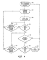
- Figure 4 illustrates a method of refreshing a plurality of memory cells 320 ( Figure 2 ) in accordance with one embodiment of the present invention.
- the computer system 250 maintains a counter having a value which corresponds to a particular address in the memory array 190.
- a first step 450 the memory cell 320 at the address corresponding to the current value of the counter is refreshed, using the method illustrated in Figure 3 or another suitable method.
- the value of the counter is incremented, and in a next step 454, a timer is reset and started.
- the processor 270 determines whether the timer has exceeded a predetermined minimum wait time.
- the appropriate value for the minimum wait time can be determined by considering a number of factors, such as, for example, the maximum time that a memory cell 320 can retain its assigned state, the time required to refresh a memory cell 320, the number of memory cells 320 to be refreshed, and the like.
- this predetermined minimum wait time can advantageously be a relatively long period of time, such as, for example, a period of seconds, minutes, hours, days, or longer.
- the predetermined minimum wait time is a period of about one minute.
- the minimum wait time is a period of about one hour.
- the minimum wait time is a period of about one day to one week.
- the processor 270 determines whether the memory cell 320 at the address corresponding to the current value of the counter needs to be refreshed.
- a number of different conditions may indicate that the memory cell 320 at the current address does not need to be refreshed. For example, as discussed above, in some embodiments, when a memory cell 320 is in the erased state, the memory cell 320 does not need to be refreshed.
- the processor 270 performs a write operation to the memory cell 320 sometime after the timer is reset and started during step 454, then the memory cell 320 does not need to be refreshed until the next memory refresh cycle.
- the processor 270 determines that the memory cell 320 at the current address does not need to be refreshed, then the process returns to step 452, where the value of the counter corresponding to the current memory address is incremented, and the process continues, as described above. On the other hand, If, once the timer reaches the minimum wait time, the memory cell 320 at the current address still needs to be refreshed, then the process proceeds to a step 460, where the processor 270 determines whether system resources are available to refresh the memory cell 320. In making this determination, the processor 270 may evaluate a wide variety of factors, such as, for example, the demands on the processor 270 and on the memory device 260 or other devices in the computer system 250, and the like.
- the process returns to step 450, where the memory cell 320 at the current address is refreshed and the process continues, as described above.
- the processor 270 determines whether the timer has exceeded a predetermined maximum wait time.
- the appropriate value for the maximum wait time can be determine by considering a number of factors, such as, for example, the maximum time that a memory cell 320 can retain its assigned state, the time required to refresh a memory cell 320, the number of memory cells 320 to be refreshed, and the like.
- this predetermined maximum wait time can advantageously be a relatively long period of time, such as, for example, a period of seconds, minutes, hours, days, weeks, or longer.
- the maximum wait time is a period of about one hour.
- the maximum wait time is a period of about one week.
- the maximum wait time is a period of about one month.
- the processor 270 determines whether the memory cell 320 at the address corresponding to the current value of the counter needs to be refreshed. As discussed above in connection with step 458, a number of different conditions may indicate that the memory cell 320 at the current address does not need to be refreshed.
- step 452 the value of the counter corresponding to the current memory address is incremented, and the process continues, as described above.
- the processor 270 continues to monitor whether system resources have become available to refresh the memory cell 320.
- step 466 the processor 270 forces certain system resources to be relinquished by other processes, such that the necessary resources become available to refresh the memory cell 320.
- the process then returns to step 450, where the memory cell 320 at the current address is refreshed, and the process continues, as described above.
- the process illustrated in Figure 4 is repeatedly performed, without interruption, by the processor 270.
- the memory refresh operation is an ongoing process, which is constantly occurring in the background of other processes being executed by the processor 270.
- the minimum wait time and the maximum wait time can advantageously be selected and adjusted such that each memory cell 320 is refreshed as infrequently as possible, while preserving the information stored in the memory device 310.
- Figure 5 illustrates another method of refreshing a plurality of memory cells 320 in accordance with one embodiment of the present invention.
- a timer is reset and started.
- the computer system 250 of Figure 2 maintains a counter having a value which corresponds to a particular address in the memory array 310 to perform the method illustrated in Figure 5 .
- the memory cell 320 at the address corresponding to the current value of the counter is refreshed, using the method illustrated in Figure 3 or another suitable method.
- the value of the counter is incremented.
- the processor 270 determines whether the memory refresh operation is complete.
- a number of conditions may indicate that the memory refresh operation is complete.
- the memory refresh operation may be considered complete when each memory cell 320 in a memory array 310 has been refreshed, or when each memory cell 320 in a particular block of memory has been refreshed.
- step 510 the processor 270 determines whether system resources are available to refresh the memory cell 320 at the address corresponding to the current value of the counter. If system resources are available, then the process returns to step 504, where the memory cell 320 at the current address is refreshed, and the process continues, as described above.
- the processor 270 determines whether the timer has exceeded a predetermined maximum wait time.
- the appropriate value for the maximum wait time can be determined by considering a number of factors, such as, for example, the maximum time that a memory cell 320 can retain its assigned state, the time required to refresh a memory cell 320, the number of memory cells 320 to be refreshed, and the like.
- this predetermined maximum wait time can advantageously be a relatively long period of time, such as, for example, a period of seconds, minutes, hours, days, weeks, or longer.
- the maximum wait time discussed above in connection with Figure 4 corresponds to the maximum time that the processor 270 can wait before it forces system resources to become available to refresh an individual memory cell 320.
- the maximum wait time corresponds to the maximum time that the processor 270 can wait before it forces system resources to become available to refresh all of the remaining memory cells 320 in the memory array 310 or in the block of memory being refreshed.
- the maximum wait time is a period of about one day.
- the maximum wait time is a period of about one week.
- the maximum wait time is a period of about one month to two months.
- process returns to step 510, where, as described above, the processor 270 continues to monitor whether system resources have become available to refresh the memory cell 320. Once the timer reaches the predetermined maximum wait time, if system resources have not become available, then the process proceeds to a step 514, where the processor 270 forces certain system resources to be relinquished by other processes, such that the necessary resources become available to refresh the memory cell 320. The process then returns to step 504, where the memory cell 320 at the current address is refreshed, and the process continues, as described above.
- step 508 the processor 270 determines that the memory refresh operation is complete. Once this determination is made, the process then proceeds to a step 516, where the memory address counter is reset. In a final step 518, the process ends.
- the process illustrated in Figure 5 is repeated by the processor 270 periodically.
- the memory refresh operation is performed periodically, rather than being a constantly ongoing process, as described above in connection with Figure 4 .
- the processor 270 can advantageously call and perform this process at regular time intervals or at irregular time intervals, depending upon the requirements of the computer system 250 and upon the longevity of the data stored in the memory cells 320.
Abstract
Description
- This invention relates generally to computer memory devices and more particularly to memory devices that must be periodically refreshed to avoid losing data.
- Certain memory devices can maintain the information stored in the memory indefinitely, even when the power to the memory device is turned off. These memory devices are known as non-volatile memory devices. Some examples of non-volatile memory devices include magnetic random access memories (MRAMs), erasable programmable read only memories (EPROMs), and variations thereof.
- Other memory devices require power to maintain the information stored in the memory. These memory devices, which are known as volatile memory devices, must be periodically refreshed to avoid losing data. One common example of a volatile memory device is a dynamic random access memory (DRAM), wherein voltages stored in capacitors represent digital bits of information. Because the voltage stored in a capacitor dissipates over time, the capacitors of a DRAM must be periodically recharged to maintain the information stored in the DRAM.
- Conventional volatile memory devices include a plurality of individual memory cells configured in an array, which typically comprises a configuration of intersecting rows and columns. To maintain the information stored in a conventional volatile memory device, each memory cell in the array is typically refreshed at least several times per second. For example, in some conventional DRAMs, each memory cell must be refreshed about once every 64 milliseconds to avoid losing the information stored in the DRAM. Accordingly, conventional volatile memory devices typically include refresh circuitry to ensure that every memory cell is refreshed at least as often as necessary to avoid losing data, which is commonly at least several times per second.
US-5.574.684 describes a refresh method for a flash memory checking whether the threshold voltage of a cell is between two voltage limits (Program W and Erase W) and if this situation occurs, refreshing the cell by programming a zero ("0") by means of a write operation. - In one embodiment, a method of refreshing a cell is specified in
claim 1. - In another aspect a memory device is specified in claim 7.
-
Figure 1 illustrates a computer system that includes a volatile memory device. -
Figure 2 illustrates a computer system having a software refreshed memory device in accordance with one embodiment of the present invention. -
Figure 3 illustrates a method of refreshing a memory cell in accordance with one embodiment of the present invention. -
Figure 4 illustrates a method of refreshing a plurality of memory cells in accordance with one embodiment of the present invention. -
Figure 5 illustrates a method of refreshing a plurality of memory cells in accordance with one embodiment of the present invention. -
Figure 1 illustrates acomputer system 100 that includes a conventionalvolatile memory device 110. Thecomputer system 100 also comprises aprocessor 120 coupled to thememory device 110 via abus 130. Thememory device 110 comprises an address/data/control module 140 andmemory refresh circuitry 150, both of which are coupled to theprocessor 120 via thebus 130. Thememory device 110 also comprises amemory array 160 coupled to the address/data/control module 140 vialine 200 and to thememory refresh circuitry 150 vialine 210. Those of ordinary skill in the art will understand thatlines memory device 110 as part of a single physical bus. Thememory array 160 comprises a plurality ofmemory cells 170; which are interconnected by a plurality of intersectingrows 180 andcolumns 190. - To perform operations in the
memory device 110, theprocessor 120 transmits certain signals to thememory device 110 via thebus 130. For example, to read data stored at a particular memory address, theprocessor 120 issues a read command, together with the memory address, to thebus 130. The address/data/control module 140 receives and processes the read command by accessing thememory array 160 vialine 200. Specifically, the address/data/control module 140 generates a read control signal online 200 and addresses the desiredmemory cell 170 by activating theappropriate row 180 andcolumn 190. The address/data/control module 140 then receives the data stored at the addressedmemory cell 170 vialine 200, and passes the data to theprocessor 120 via thebus 130. - In addition, to write data to a particular memory address, the
processor 120 issues a write command, together with the memory address and the data to be stored, to thebus 130. The address/data/control module 140 receives and processes the write command by generating a write control signal online 200 and addressing the desiredmemory cell 170, as described above. The address/data/control module 140 then passes the data to be stored to the addressedmemory cell 170 vialine 200. - Because the data stored in the
memory cells 170 dissipates over time, thememory cells 170 must be periodically refreshed to avoid losing the data stored in thememory device 110. The primary function of thememory refresh circuitry 150 is to perform these periodic memory refresh operations. When thememory refresh circuitry 150 determines that it is necessary to perform a memory refresh operation, thememory device 110 is made unavailable to theprocessor 120 to perform other operations, such as a read operation or a write operation. - To perform a memory refresh operation, the
memory refresh circuitry 150 typically sequentially addresses therows 180 of thememory array 160. When a givenrow 180 of thearray 160 is addressed, the memory refresh circuitry generates a refresh control signal online 210, which causes all of thememory cells 170 in the addressedrow 180 to be refreshed simultaneously. By refreshing a large number ofmemory cells 170 simultaneously, thememory refresh circuitry 150 advantageously reduces the amount of time required to perform a memory refresh operation, thereby reducing the amount of time that thememory device 110 is unavailable to theprocessor 120 to perform other operations. - Because the
memory device 110 is unavailable to perform other operations during a memory refresh operation, it is desirable to time memory refresh operations such that they occur at times when they will not conflict with requests from theprocessor 120. Therefore, thememory refresh circuitry 150 is often configured to identify time periods when theprocessor 120 is not likely to issue requests to thememory device 110, and to perform memory refresh operations during these identified time periods. On the other hand, because power is required to perform a memory refresh operation, it is desirable to minimize the number of memory refresh operations performed. Thus, thememory refresh circuitry 150 is also often configured to perform memory refresh operations as infrequently as possible, while preserving the data stored in thememory device 110. - Nevertheless, to avoid losing data stored in conventional
volatile memory devices 110, thememory refresh circuitry 150 must perform memory refresh operations frequently, often many times per second. For example, in some embodiments, eachmemory cell 170 must be refreshed at least about once every 64 milliseconds to avoid losing data. In these embodiments, to avoid losing the information stored in thememory device 110, thememory refresh circuitry 150 must ensure that everymemory cell 170 is refreshed at least more often than about 15 times per second. -
Figure 2 illustrates acomputer system 250 having a software refreshedmemory device 260 in accordance with one embodiment of the present invention. Thecomputer system 250 also comprises aprocessor 270 coupled to thememory device 260 via abus 280. Thecomputer system 250 further comprises a set ofmemory refresh instructions 290, which are implemented in software that can be executed by theprocessor 270. Thememory device 260 comprises an address/data/control module 300 which is coupled to theprocessor 270 via thebus 280. Thememory device 260 also comprises amemory array 310 coupled to the address/data/control module 300 vialine 350. Thememory array 310 comprises a plurality ofmemory cells 320, which are interconnected by a plurality of intersectingrows 330 andcolumns 340. - The
computer system 250 illustrated inFigure 2 can perform memory read and write operations using the same methods described above in connection withFigure 1 . In addition to these methods, however, thecomputer system 250 can perform memory read and write operations in a variety of other ways that are well-known to those of ordinary skill in the art. - In some embodiments, the
memory cells 320 of the software refreshedmemory device 260 comprise volatile memory cells, which are preferably more stable than conventional DRAM memory cells. For example, in one embodiment, thememory cells 320 can avoid losing data even though the time interval between successive memory refresh operations is about 0.1 seconds. In another embodiment, the time interval between successive memory refresh operations can be about one second. In yet another embodiment, the time interval between successive memory refresh operations can be about one hour. In yet another embodiment, the time interval between successive memory refresh operations can be about one day to one week. - In some embodiments, the
memory cells 320 of the software refreshedmemory device 260 comprise programmable conductor random access memory (PCRAM) cells, which are described inU.S. Patent Nos. 5,761,115 ,5,896,312 ,5,914,893 ,6,084,796 to Kozicki et al . ("the Kozicki patents"), inU.S. Patent No. 6,348,365 to Moore et al . ("the Moore patent"), and in the followingU.S. patent Nos. 6.858.482 entitled "Method of Manufacture of Programmable Conductor Memory" filed April 10, 2002,6.864.500 entitled "Programmable Conductor Memory Cell Structure and Method Therefor" filed April 10, 2002, and6.855.975 entitled "Thin Film Diode Integrated with Chalcogenide Memory Cell" filed April 10, 2002. As discussed in more detail in these references, a PCRAM cell comprises a pair of electrodes and can exist in one of two possible states. In the first state, an electrical short exists between the electrodes of the PCRAM cell In the second state, an open circuit exists between the electrodes of the PCRAM cell. - Some embodiments of a PCRAM cell comprise a glass ion conductor, such as a chalcogenide-metal ion glass, and two electrodes disposed at the surface of the glass ion conductor and spaced a distance apart from one another. In one embodiment, a PCRAM cell comprises germanium selenide with a Group IV metal (e.g., silver) dissolved therein, such as Ag/Gc3Se7. Preferably, one of the electrodes comprises a Group IV metal, and the glass element of the PCRAM cell contains the same metal.
- In operation, when a voltage having a first polarity is applied across the electrodes of a PCRAM cell, a conductive path is created between the electrodes along the sidewalls of the via in which the glass element is formed. When a voltage having the opposite polarity is applied across the electrodes, the metal ions re-dissolve into the cell body, thereby causing the conductive path to disappear. The presence or absence of a conductive path within a PCRAM cell can be detected by measuring the electrical resistance between the electrodes. When a conductive path is present, an electrical short exists between the electrodes, and the resistance between the electrodes is low (e.g., on the order of milliohms). On the other hand, when no conductive path is present, an open circuit exists between the electrodes, and the resistance between the electrodes is high (e.g., on the order of megaohms).
- The features of
Figure 2 are referenced throughout the discussion below of operation processes. - Typically, the
memory cells 320 of thememory device 260 are capable of existing in one of two states, i.e., a "written" state or an "erased" state. For example, if amemory cell 320 comprises a capacitor capable of holding a charge, the presence of a charge in the capacitor would correspond to the written state, and the absence of a charge in the capacitor would correspond to the erased state. Similarly, if a PCRAM cell acts as amemory cell 320, the presence of a conductive path between the electrodes would correspond to the written state, while the absence of a conductive path between the electrodes would correspond to the erased state. Those of ordinary skill in the art will understand that, in general, the presence of an element of interest within amemory cell 320 will correspond to the written state, whereas the absence of an element of interest will correspond to the erased state. - As discussed above in connection with
Figure 1 , when amemory cell 170 of a conventionalvolatile memory device 110 is placed in a particular state, thememory cell 170 remains in the given state for a relatively short period of time, such as, for example, about 64 milliseconds. Because suchconventional memory cells 170 retain their assigned states for such a short time period, eachmemory cell 170 must be refreshed often, such as, for example, at least more often than about 15 times per second. - By contrast, when a
memory cell 320 of the software refreshedmemory device 260 illustrated inFigure 2 is placed in a particular state, thememory cell 320 advantageously remains in the given state for a relatively long period of time. For example, in some embodiments, eachmemory cell 320 can maintain a given state for a period of seconds, minutes, hours, days, weeks, or longer. Accordingly, the data stored in thememory device 260 can be preserved while performing memory refresh operations less frequently, such as, for example, about once every few weeks, rather than several times per second. - Because memory refresh operations can occur less frequently, the
computer system 250 can advantageously perform these memory refresh operations by executing a set ofmemory refresh instructions 290 implemented in software, rather than in hardware. For example, in some embodiments, thememory refresh instructions 290 constitute part of the operating system of thecomputer system 250. - By implementing the
memory refresh instructions 290 in software, rather than in hardware, thememory device 260 can advantageously be simplified. For example, the need for thememory refresh circuitry 150 and for a unique refresh control signal online 210, as illustrated inFigure 1 , are advantageously eliminated. Another advantage of implementing thememory refresh instructions 290 in software, rather than in hardware, is that the processor 270 (Figure 2 ) can perform more sophisticated algorithms, as compared to the memory refresh circuitry 150 (Figure 1 ), for determining when to perform a memory refresh operation. -
Figure 3 illustrates a method of refreshing a memory cell 320 (Figure 2 ) in accordance with one embodiment of the present invention. In afirst step 400, the process begins. In anext step 402, theprocessor 270 reads the state of thememory cell 320. The state of thememory cell 320 is assigned a logical value, which corresponds to a digital bit of data. For example, in some embodiments, the written state of amemory cell 320 may correspond to a logical "1", while the erased state of thememory cell 320 corresponds to a logical "0". In some alternative embodiments, on the other hand, the written state of amemory cell 320 may correspond to a logical "0", while the erased state of thememory cell 320 corresponds to a logical "1". - In a
step 404, theprocessor 270 determines whether the data bit stored in thememory cell 320 is a "1" or a "0". If the data bit is a "1", then, in astep 406, theprocessor 270 writes a "1" to thememory cell 320. For example, if a "1" corresponds to the written state, then, duringstep 406, theprocessor 270 issues a "write instruction" to the memory cell, i.e., a write command, is issued, and thememory cell 320 is placed in the written state. If, duringstep 404, theprocessor 270 determines that the data bit stored in thememory cell 320 is a "0", then, in astep 408, theprocessor 270 writes a "0" to thememory cell 320. For example, if a "0" corresponds to the erased state, then, duringstep 408, theprocessor 270 issues an "erase instruction" to the memory cell, i.e., a write command is issued, and thememory cell 320 is placed in the erased state. - A write instruction issued during a memory refresh operation can be the same as a write instruction issued during a standard write operation to the
memory device 260. Similarly, an erase instruction issued during a memory refresh operation can be the same as an erase instruction issued during a standard write operation to thememory device 260. Accordingly, as discussed above, the need for a unique refresh control signal, which is utilized only during memory refresh operations, is advantageously eliminated. After theprocessor 270 completesstep 406 or step 408, then, in afinal step 410, the process ends. - In the method illustrated in
Figure 3 , it is assumed that a memory cell 320 (Figure 2 ) will not remain in the written state or in the erased state indefinitely unless it is periodically refreshed by issuing a write instruction or an erase instruction, whichever is appropriate, to thememory cell 320. In some embodiments, however, thememory cells 320 tend to revert to one particular state over time. For example, in some embodiments, thememory cells 320 tend to revert to the erased state over time. In these embodiments, when amemory cell 320 is placed in the written state, thememory cell 320 will not remain in the written state indefinitely unless it is periodically refreshed by performing a write operation on thememory cell 320. On the other hand, because the natural tendency of thememory cells 320 is to revert to the erased state, amemory cell 320 placed in the erased state will remain in this stale indefinitely, without needing to be refreshed. In these embodiments, the method illustrated inFigure 3 can advantageously be simplified by eliminating either step 406 or step 408, whichever corresponds to the erased state. - Moreover, in the method illustrated in
Figure 3 , it is assumed that each memory cell 320 (Figure 2 ) is capable of existing in one of only two states. Nevertheless, in light of the present disclosure, those of ordinary skill in the art will understand how the method illustrated inFigure 3 can be modified if thememory cells 320 are capable of existing in more than two states. - If a memory refresh operation comprises the method illustrated in
Figure 3 , then each memory cell 320 (Figure 2 ) is refreshed individually, rather than refreshing a large number ofmemory cells 320 simultaneously, as discussed above in connection withFigure 1 . By evaluating eachmemory cell 320 individually, theprocessor 270 can determine whether eachindividual memory cell 320 needs to be refreshed, thereby advantageously avoiding performing unnecessary refresh operations onmemory cells 320 that do not need to be refreshed. -
Figure 4 illustrates a method of refreshing a plurality of memory cells 320 (Figure 2 ) in accordance with one embodiment of the present invention. To perform this method, thecomputer system 250 maintains a counter having a value which corresponds to a particular address in thememory array 190. In afirst step 450, thememory cell 320 at the address corresponding to the current value of the counter is refreshed, using the method illustrated inFigure 3 or another suitable method. In anext step 452, the value of the counter is incremented, and in anext step 454, a timer is reset and started. - In a
step 456, theprocessor 270 determines whether the timer has exceeded a predetermined minimum wait time. The appropriate value for the minimum wait time can be determined by considering a number of factors, such as, for example, the maximum time that amemory cell 320 can retain its assigned state, the time required to refresh amemory cell 320, the number ofmemory cells 320 to be refreshed, and the like. As discussed above, this predetermined minimum wait time can advantageously be a relatively long period of time, such as, for example, a period of seconds, minutes, hours, days, or longer. In one embodiment, the predetermined minimum wait time is a period of about one minute. In another embodiment, the minimum wait time is a period of about one hour. In yet another embodiment, the minimum wait time is a period of about one day to one week. - If the minimum wait time has not yet been reached, then, in a
step 458, theprocessor 270 determines whether thememory cell 320 at the address corresponding to the current value of the counter needs to be refreshed. A number of different conditions may indicate that thememory cell 320 at the current address does not need to be refreshed. For example, as discussed above, in some embodiments, when amemory cell 320 is in the erased state, thememory cell 320 does not need to be refreshed. Moreover, if theprocessor 270 performs a write operation to thememory cell 320 sometime after the timer is reset and started duringstep 454, then thememory cell 320 does not need to be refreshed until the next memory refresh cycle. - If, while waiting for the timer to reach the minimum wait time, the
processor 270 determines that thememory cell 320 at the current address does not need to be refreshed, then the process returns to step 452, where the value of the counter corresponding to the current memory address is incremented, and the process continues, as described above. On the other hand, If, once the timer reaches the minimum wait time, thememory cell 320 at the current address still needs to be refreshed, then the process proceeds to astep 460, where theprocessor 270 determines whether system resources are available to refresh thememory cell 320. In making this determination, theprocessor 270 may evaluate a wide variety of factors, such as, for example, the demands on theprocessor 270 and on thememory device 260 or other devices in thecomputer system 250, and the like. - If system resources are available, then the process returns to step 450, where the
memory cell 320 at the current address is refreshed and the process continues, as described above. On the other hand, if system resources are not available to refresh thememory cell 320, then, in astep 462, theprocessor 270 determines whether the timer has exceeded a predetermined maximum wait time. As with the minimum wait time, the appropriate value for the maximum wait time can be determine by considering a number of factors, such as, for example, the maximum time that amemory cell 320 can retain its assigned state, the time required to refresh amemory cell 320, the number ofmemory cells 320 to be refreshed, and the like. As discussed above, this predetermined maximum wait time can advantageously be a relatively long period of time, such as, for example, a period of seconds, minutes, hours, days, weeks, or longer. In one embodiment, the maximum wait time is a period of about one hour. In another embodiment, the maximum wait time is a period of about one week. In yet another embodiment, the maximum wait time is a period of about one month. - If the maximum wait time has not yet been reached, then, in a
step 464, theprocessor 270 determines whether thememory cell 320 at the address corresponding to the current value of the counter needs to be refreshed. As discussed above in connection withstep 458, a number of different conditions may indicate that thememory cell 320 at the current address does not need to be refreshed. - If the
memory cell 320 at the current address does not need to be refreshed, then the process returns to step 452, where the value of the counter corresponding to the current memory address is incremented, and the process continues, as described above. On the other hand, if thememory cell 320 at the current address needs to be refreshed, then theprocessor 270 continues to monitor whether system resources have become available to refresh thememory cell 320. - Once the timer reaches the predetermined maximum wait time, if system resources have not become available and the
memory cell 320 at the current address still needs to be refreshed, then the process proceeds to astep 466, where theprocessor 270 forces certain system resources to be relinquished by other processes, such that the necessary resources become available to refresh thememory cell 320. The process then returns to step 450, where thememory cell 320 at the current address is refreshed, and the process continues, as described above. - In one embodiment, the process illustrated in
Figure 4 is repeatedly performed, without interruption, by theprocessor 270. In this embodiment, the memory refresh operation is an ongoing process, which is constantly occurring in the background of other processes being executed by theprocessor 270. The minimum wait time and the maximum wait time can advantageously be selected and adjusted such that eachmemory cell 320 is refreshed as infrequently as possible, while preserving the information stored in thememory device 310. -
Figure 5 illustrates another method of refreshing a plurality ofmemory cells 320 in accordance with one embodiment of the present invention. In afirst step 500, the process begins, and in anext step 502, a timer is reset and started. As with the method illustrated inFigure 4 , thecomputer system 250 ofFigure 2 maintains a counter having a value which corresponds to a particular address in thememory array 310 to perform the method illustrated inFigure 5 . In astep 504, thememory cell 320 at the address corresponding to the current value of the counter is refreshed, using the method illustrated inFigure 3 or another suitable method. In anext step 506, the value of the counter is incremented. - In a
step 508, theprocessor 270 determines whether the memory refresh operation is complete. A number of conditions may indicate that the memory refresh operation is complete. For example, the memory refresh operation may be considered complete when eachmemory cell 320 in amemory array 310 has been refreshed, or when eachmemory cell 320 in a particular block of memory has been refreshed. - If the memory refresh operation is not yet complete, then, in a
step 510, theprocessor 270 determines whether system resources are available to refresh thememory cell 320 at the address corresponding to the current value of the counter. If system resources are available, then the process returns to step 504, where thememory cell 320 at the current address is refreshed, and the process continues, as described above. - On the other hand, if system resources are not available to refresh the
memory cell 320, then, in astep 512, theprocessor 270 determines whether the timer has exceeded a predetermined maximum wait time. As discussed above in connection withFigure 4 , the appropriate value for the maximum wait time can be determined by considering a number of factors, such as, for example, the maximum time that amemory cell 320 can retain its assigned state, the time required to refresh amemory cell 320, the number ofmemory cells 320 to be refreshed, and the like. Moreover, as discussed above, this predetermined maximum wait time can advantageously be a relatively long period of time, such as, for example, a period of seconds, minutes, hours, days, weeks, or longer. - In one embodiment, the maximum wait time discussed above in connection with
Figure 4 corresponds to the maximum time that theprocessor 270 can wait before it forces system resources to become available to refresh anindividual memory cell 320. In the process illustrated inFigure 5 , on the other hand, the maximum wait time corresponds to the maximum time that theprocessor 270 can wait before it forces system resources to become available to refresh all of the remainingmemory cells 320 in thememory array 310 or in the block of memory being refreshed. Thus, in one embodiment, the maximum wait time is a period of about one day. In another embodiment, the maximum wait time is a period of about one week. In yet another embodiment, the maximum wait time is a period of about one month to two months. - If the maximum wait time has not yet been reached, then process returns to step 510, where, as described above, the
processor 270 continues to monitor whether system resources have become available to refresh thememory cell 320. Once the timer reaches the predetermined maximum wait time, if system resources have not become available, then the process proceeds to astep 514, where theprocessor 270 forces certain system resources to be relinquished by other processes, such that the necessary resources become available to refresh thememory cell 320. The process then returns to step 504, where thememory cell 320 at the current address is refreshed, and the process continues, as described above. - This process repeats until, during
step 508, theprocessor 270 determines that the memory refresh operation is complete. Once this determination is made, the process then proceeds to astep 516, where the memory address counter is reset. In afinal step 518, the process ends. - In one embodiment, the process illustrated in
Figure 5 is repeated by theprocessor 270 periodically. In this embodiment, the memory refresh operation is performed periodically, rather than being a constantly ongoing process, as described above in connection withFigure 4 . Theprocessor 270 can advantageously call and perform this process at regular time intervals or at irregular time intervals, depending upon the requirements of thecomputer system 250 and upon the longevity of the data stored in thememory cells 320. - The processes illustrated in
Figures 3 ,4 and5 are merely examples of algorithms that can be implemented in thememory refresh instructions 290. Those of ordinary skill in the art will understand that these exemplary algorithms can be easily modified by adding, removing, or varying certain steps. Moreover, in light of the present disclosure, those of ordinary skill in the art will understand how to develop a wide variety of alternative algorithms.
Claims (12)
- A method of refreshing a memory cell (170) of a memory array (160), the method comprising:for a plurality of memory cells of said memory array (160), determining whether each individual memory cell of said plurality of memory cells requires a refresh;determining whether a given cell (170) requiring a refresh is in a written state or in an erased state; andif said given cell (170) is in said written state, individually refreshing said given cell (170) by issuing a refresh write instruction to said given cell;
characterised in that
said refresh write instruction is the same instruction during the refresh operation and during the write operation;waiting for a first period of time since said given cell (170) was refreshed; anddetermining whether said given cell (170) requires another refresh. - The method of Claim 1, further comprising, of said given cell (170) is in said erased state, refreshing said given cell by issuing a refresh erase instruction to said given cell (170).
- The method of claim 1, comprising:addressing said given cell (170);if said given cell (170) needs to be refreshed, determining whether system resources are available to refresh said given cell (170);if said given cell (170) needs to be refreshed and if said system resources are not available, monitoring whether said system resources become available to refresh said given cell (170) within a second period of time since said given cell (170) was refreshed;if said given cell (170) needs to be refreshed and if said system resources do not become available within said second period of time, forcing said resources to be relinquished, such that said resources become available to refresh said given cell (170); andif said given cell (170) needs to be refreshed, refreshing said given cell (170) using said available system resources.
- The method of claim 3, wherein said first period of time is within the range of approximately one second to approximately one week.
- The method of claim 3 or 4, wherein said second period of time is within the range of approximately one week to approximately two months.
- The method of claim 3, wherein the steps of accessing said given cell (170) of said plurality of memory cells is for each of said plurality of memory cells of a memory array (160).
- Apparatus comprising a processor (120) and memory device (110) comprising a plurality of cells that must be periodically refreshed, wherein each of said plurality of cells in a written state is configured to be individually refreshed via a write instruction received from the processor (120), wherein said processor (120) is configured to determine whether each individual cell (170) of said plurality of cells needs to be refreshed, wherein said write instruction is the same instruction during a refresh operation and during a write operation, and wherein said processor (120) is also configured to wait a period of time since a first individual memory cell (170) was refreshed and to determine whether said first individual memory cell (170) was refreshed and to determines whether said first individual memory cell (170) needs to be refreshed again.
- The apparatus of claim 7, wherein each of said plurality of cells in an erased state is configured to be individually refreshed via an erase instruction received from the processor, wherein said erase instruction is the same instruction during a refresh operation and during an erase operation.
- The apparatus of claim 8, wherein said memory device comprises a programmable conductor random access memory cell.
- The apparatus of claim 9, wherein said programmable conductor random access memory cell comprises:a cell body having a top surface, wherein said cell body comprises a chalcogenide-metal ion glass; andtwo electrodes disposed at said top surface, wherein said electrodes are spaced a distance apart from one another.
- The apparatus of claim 10, wherein said chalcogenide-metal ion glass comprises germanium selenide having a Group IV metal dissolved therein.
- The apparatus of claim 11, wherein said chalcogenide-metal ion glass comprises Ag/Ge3Se7.
Priority Applications (1)
| Application Number | Priority Date | Filing Date | Title |
|---|---|---|---|
| EP10075616A EP2293305B1 (en) | 2002-08-29 | 2003-08-28 | Memory device refreshed by force and method |
Applications Claiming Priority (3)
| Application Number | Priority Date | Filing Date | Title |
|---|---|---|---|
| US234001 | 2002-08-29 | ||
| US10/234,001 US7010644B2 (en) | 2002-08-29 | 2002-08-29 | Software refreshed memory device and method |
| PCT/US2003/027056 WO2004021359A2 (en) | 2002-08-29 | 2003-08-28 | Software refreshed memory device and method |
Related Child Applications (1)
| Application Number | Title | Priority Date | Filing Date |
|---|---|---|---|
| EP10075616.2 Division-Into | 2010-10-01 |
Publications (2)
| Publication Number | Publication Date |
|---|---|
| EP1540657A2 EP1540657A2 (en) | 2005-06-15 |
| EP1540657B1 true EP1540657B1 (en) | 2011-07-20 |
Family
ID=31977345
Family Applications (2)
| Application Number | Title | Priority Date | Filing Date |
|---|---|---|---|
| EP10075616A Expired - Lifetime EP2293305B1 (en) | 2002-08-29 | 2003-08-28 | Memory device refreshed by force and method |
| EP03749204A Expired - Lifetime EP1540657B1 (en) | 2002-08-29 | 2003-08-28 | Software refreshed memory device and method |
Family Applications Before (1)
| Application Number | Title | Priority Date | Filing Date |
|---|---|---|---|
| EP10075616A Expired - Lifetime EP2293305B1 (en) | 2002-08-29 | 2003-08-28 | Memory device refreshed by force and method |
Country Status (9)
| Country | Link |
|---|---|
| US (5) | US7010644B2 (en) |
| EP (2) | EP2293305B1 (en) |
| JP (1) | JP4891544B2 (en) |
| KR (1) | KR100626933B1 (en) |
| CN (1) | CN100483546C (en) |
| AT (2) | ATE557398T1 (en) |
| AU (1) | AU2003268251A1 (en) |
| TW (1) | TWI263221B (en) |
| WO (1) | WO2004021359A2 (en) |
Families Citing this family (50)
| Publication number | Priority date | Publication date | Assignee | Title |
|---|---|---|---|---|
| US6560155B1 (en) * | 2001-10-24 | 2003-05-06 | Micron Technology, Inc. | System and method for power saving memory refresh for dynamic random access memory devices after an extended interval |
| US7010644B2 (en) * | 2002-08-29 | 2006-03-07 | Micron Technology, Inc. | Software refreshed memory device and method |
| DE102004018859B3 (en) * | 2004-04-19 | 2005-09-15 | Infineon Technologies Ag | Memory storage circuit e.g. for flip flop circuit for making available video or audio data for given length of time in terminal, has memory cell with PMC resistor having solid electrolyte material with write circuit |
| US8531863B2 (en) * | 2005-05-20 | 2013-09-10 | Adesto Technologies Corporation | Method for operating an integrated circuit having a resistivity changing memory cell |
| JP4813264B2 (en) | 2006-06-14 | 2011-11-09 | 株式会社日立製作所 | Storage system |
| KR100875292B1 (en) * | 2006-09-19 | 2008-12-23 | 삼성전자주식회사 | Flash memory device and its refresh method |
| US7539050B2 (en) * | 2006-11-22 | 2009-05-26 | Qimonda North America Corp. | Resistive memory including refresh operation |
| US8042022B2 (en) * | 2007-03-08 | 2011-10-18 | Micron Technology, Inc. | Method, system, and apparatus for distributed decoding during prolonged refresh |
| JP5159224B2 (en) * | 2007-09-21 | 2013-03-06 | 株式会社東芝 | Resistance change memory device |
| US8486552B2 (en) | 2008-06-30 | 2013-07-16 | Lg Chem, Ltd. | Battery module having cooling manifold with ported screws and method for cooling the battery module |
| US9759495B2 (en) | 2008-06-30 | 2017-09-12 | Lg Chem, Ltd. | Battery cell assembly having heat exchanger with serpentine flow path |
| JP5262402B2 (en) * | 2008-08-04 | 2013-08-14 | 富士通株式会社 | Storage device and data holding method |
| US7825479B2 (en) * | 2008-08-06 | 2010-11-02 | International Business Machines Corporation | Electrical antifuse having a multi-thickness dielectric layer |
| US9755705B2 (en) | 2008-08-07 | 2017-09-05 | Qualcomm Incorporated | Method and apparatus for supporting multi-user and single-user MIMO in a wireless communication system |
| US9294160B2 (en) | 2008-08-11 | 2016-03-22 | Qualcomm Incorporated | Method and apparatus for supporting distributed MIMO in a wireless communication system |
| US8663829B2 (en) | 2009-04-30 | 2014-03-04 | Lg Chem, Ltd. | Battery systems, battery modules, and method for cooling a battery module |
| US8403030B2 (en) | 2009-04-30 | 2013-03-26 | Lg Chem, Ltd. | Cooling manifold |
| EP2273365A1 (en) * | 2009-06-26 | 2011-01-12 | Thomson Licensing | Combined memory and storage device in an apparatus for data processing |
| US8399118B2 (en) | 2009-07-29 | 2013-03-19 | Lg Chem, Ltd. | Battery module and method for cooling the battery module |
| US8399119B2 (en) | 2009-08-28 | 2013-03-19 | Lg Chem, Ltd. | Battery module and method for cooling the battery module |
| US9411674B2 (en) * | 2010-03-19 | 2016-08-09 | Microsoft Technology Licensing, Llc | Providing hardware resources having different reliabilities for use by an application |
| US8412882B2 (en) | 2010-06-18 | 2013-04-02 | Microsoft Corporation | Leveraging chip variability |
| US8662153B2 (en) | 2010-10-04 | 2014-03-04 | Lg Chem, Ltd. | Battery cell assembly, heat exchanger, and method for manufacturing the heat exchanger |
| US8756474B2 (en) * | 2011-03-21 | 2014-06-17 | Denso International America, Inc. | Method for initiating a refresh operation in a solid-state nonvolatile memory device |
| US9379420B2 (en) | 2012-03-29 | 2016-06-28 | Lg Chem, Ltd. | Battery system and method for cooling the battery system |
| US9105950B2 (en) | 2012-03-29 | 2015-08-11 | Lg Chem, Ltd. | Battery system having an evaporative cooling member with a plate portion and a method for cooling the battery system |
| US9605914B2 (en) | 2012-03-29 | 2017-03-28 | Lg Chem, Ltd. | Battery system and method of assembling the battery system |
| US8852781B2 (en) | 2012-05-19 | 2014-10-07 | Lg Chem, Ltd. | Battery cell assembly and method for manufacturing a cooling fin for the battery cell assembly |
| CN104662609A (en) * | 2012-06-07 | 2015-05-27 | 富士通株式会社 | Control device that selectively refreshes memory |
| US9306199B2 (en) | 2012-08-16 | 2016-04-05 | Lg Chem, Ltd. | Battery module and method for assembling the battery module |
| KR102050473B1 (en) | 2012-09-24 | 2019-11-29 | 삼성전자주식회사 | Semiconductor memory device controlling refresh period and memory system |
| US8972652B2 (en) * | 2012-11-19 | 2015-03-03 | Spansion Llc | Data refresh in non-volatile memory |
| US9083066B2 (en) | 2012-11-27 | 2015-07-14 | Lg Chem, Ltd. | Battery system and method for cooling a battery cell assembly |
| US8852783B2 (en) | 2013-02-13 | 2014-10-07 | Lg Chem, Ltd. | Battery cell assembly and method for manufacturing the battery cell assembly |
| US9647292B2 (en) | 2013-04-12 | 2017-05-09 | Lg Chem, Ltd. | Battery cell assembly and method for manufacturing a cooling fin for the battery cell assembly |
| US9184424B2 (en) | 2013-07-08 | 2015-11-10 | Lg Chem, Ltd. | Battery assembly |
| US9257732B2 (en) | 2013-10-22 | 2016-02-09 | Lg Chem, Ltd. | Battery cell assembly |
| US9444124B2 (en) | 2014-01-23 | 2016-09-13 | Lg Chem, Ltd. | Battery cell assembly and method for coupling a cooling fin to first and second cooling manifolds |
| US10084218B2 (en) | 2014-05-09 | 2018-09-25 | Lg Chem, Ltd. | Battery pack and method of assembling the battery pack |
| US10770762B2 (en) | 2014-05-09 | 2020-09-08 | Lg Chem, Ltd. | Battery module and method of assembling the battery module |
| US9484559B2 (en) | 2014-10-10 | 2016-11-01 | Lg Chem, Ltd. | Battery cell assembly |
| US9412980B2 (en) | 2014-10-17 | 2016-08-09 | Lg Chem, Ltd. | Battery cell assembly |
| US9786894B2 (en) | 2014-11-03 | 2017-10-10 | Lg Chem, Ltd. | Battery pack |
| US9627724B2 (en) | 2014-12-04 | 2017-04-18 | Lg Chem, Ltd. | Battery pack having a cooling plate assembly |
| JP6180450B2 (en) * | 2015-02-02 | 2017-08-16 | キヤノン株式会社 | Control device, control method and program for control device |
| US9679632B2 (en) * | 2015-04-08 | 2017-06-13 | Khalifa University of Science and Technology | Volatile memory erasure by the randomization of data stored in memory cells |
| KR102474937B1 (en) * | 2016-03-21 | 2022-12-07 | 에스케이하이닉스 주식회사 | Data storage device and operating method thereof |
| US11456033B2 (en) | 2018-09-12 | 2022-09-27 | Micron Technology, Inc. | Dedicated commands for memory operations |
| US10622065B2 (en) * | 2018-09-12 | 2020-04-14 | Micron Technology, Inc. | Dedicated commands for memory operations |
| US10777297B2 (en) * | 2018-12-10 | 2020-09-15 | Micron Technology, Inc. | Age-based refresh of firmware |
Citations (3)
| Publication number | Priority date | Publication date | Assignee | Title |
|---|---|---|---|---|
| US5497140A (en) * | 1992-08-12 | 1996-03-05 | Micron Technology, Inc. | Electrically powered postage stamp or mailing or shipping label operative with radio frequency (RF) communication |
| US5768193A (en) * | 1996-06-17 | 1998-06-16 | Aplus Integrated Circuits, Inc. | Bit-refreshable method and circuit for refreshing a nonvolatile flash memory |
| US6396744B1 (en) * | 2000-04-25 | 2002-05-28 | Multi Level Memory Technology | Flash memory with dynamic refresh |
Family Cites Families (186)
| Publication number | Priority date | Publication date | Assignee | Title |
|---|---|---|---|---|
| US4737A (en) * | 1846-09-03 | Window-sash fastener | ||
| US3271591A (en) | 1963-09-20 | 1966-09-06 | Energy Conversion Devices Inc | Symmetrical current controlling device |
| US3622319A (en) | 1966-10-20 | 1971-11-23 | Western Electric Co | Nonreflecting photomasks and methods of making same |
| US3868651A (en) | 1970-08-13 | 1975-02-25 | Energy Conversion Devices Inc | Method and apparatus for storing and reading data in a memory having catalytic material to initiate amorphous to crystalline change in memory structure |
| US3743847A (en) | 1971-06-01 | 1973-07-03 | Motorola Inc | Amorphous silicon film as a uv filter |
| US4267261A (en) | 1971-07-15 | 1981-05-12 | Energy Conversion Devices, Inc. | Method for full format imaging |
| US3961314A (en) | 1974-03-05 | 1976-06-01 | Energy Conversion Devices, Inc. | Structure and method for producing an image |
| US3966317A (en) | 1974-04-08 | 1976-06-29 | Energy Conversion Devices, Inc. | Dry process production of archival microform records from hard copy |
| US4177474A (en) | 1977-05-18 | 1979-12-04 | Energy Conversion Devices, Inc. | High temperature amorphous semiconductor member and method of making the same |
| JPS5565365A (en) | 1978-11-07 | 1980-05-16 | Nippon Telegr & Teleph Corp <Ntt> | Pattern forming method |
| DE2901303C2 (en) | 1979-01-15 | 1984-04-19 | Max Planck Gesellschaft Zur Foerderung Der Wissenschaften E.V., 3400 Goettingen | Solid ionic conductor material, its use and process for its manufacture |
| US4317169A (en) | 1979-02-14 | 1982-02-23 | Honeywell Information Systems Inc. | Data processing system having centralized memory refresh |
| US4312938A (en) | 1979-07-06 | 1982-01-26 | Drexler Technology Corporation | Method for making a broadband reflective laser recording and data storage medium with absorptive underlayer |
| US4269935A (en) | 1979-07-13 | 1981-05-26 | Ionomet Company, Inc. | Process of doping silver image in chalcogenide layer |
| FR2465269B1 (en) * | 1979-09-12 | 1985-12-27 | Cii Honeywell Bull | ASYNCHRONOUS REQUEST SELECTOR IN AN INFORMATION PROCESSING SYSTEM |
| US4316946A (en) | 1979-12-03 | 1982-02-23 | Ionomet Company, Inc. | Surface sensitized chalcogenide product and process for making and using the same |
| US4499557A (en) | 1980-10-28 | 1985-02-12 | Energy Conversion Devices, Inc. | Programmable cell for use in programmable electronic arrays |
| US4459660A (en) | 1981-04-13 | 1984-07-10 | Texas Instruments Incorporated | Microcomputer with automatic refresh of on-chip dynamic RAM transparent to CPU |
| US4405710A (en) | 1981-06-22 | 1983-09-20 | Cornell Research Foundation, Inc. | Ion beam exposure of (g-Gex -Se1-x) inorganic resists |
| US4737379A (en) | 1982-09-24 | 1988-04-12 | Energy Conversion Devices, Inc. | Plasma deposited coatings, and low temperature plasma method of making same |
| US4545111A (en) | 1983-01-18 | 1985-10-08 | Energy Conversion Devices, Inc. | Method for making, parallel preprogramming or field programming of electronic matrix arrays |
| US4608296A (en) | 1983-12-06 | 1986-08-26 | Energy Conversion Devices, Inc. | Superconducting films and devices exhibiting AC to DC conversion |
| US4625296A (en) | 1984-01-17 | 1986-11-25 | The Perkin-Elmer Corporation | Memory refresh circuit with varying system transparency |
| FR2561414B1 (en) * | 1984-03-16 | 1986-09-19 | Thomson Csf | DYNAMIC RAM AND MICROPROCESSOR SYSTEM WITH SOFTWARE COOLING. APPLICATION TO A DISTURBANCE RECORDER |
| GB8409022D0 (en) | 1984-04-06 | 1984-05-16 | Qmc Ind Res | Information holding device |
| US4795657A (en) | 1984-04-13 | 1989-01-03 | Energy Conversion Devices, Inc. | Method of fabricating a programmable array |
| US4668968A (en) | 1984-05-14 | 1987-05-26 | Energy Conversion Devices, Inc. | Integrated circuit compatible thin film field effect transistor and method of making same |
| US4673957A (en) | 1984-05-14 | 1987-06-16 | Energy Conversion Devices, Inc. | Integrated circuit compatible thin film field effect transistor and method of making same |
| US4843443A (en) | 1984-05-14 | 1989-06-27 | Energy Conversion Devices, Inc. | Thin film field effect transistor and method of making same |
| US4769338A (en) | 1984-05-14 | 1988-09-06 | Energy Conversion Devices, Inc. | Thin film field effect transistor and method of making same |
| US4670763A (en) | 1984-05-14 | 1987-06-02 | Energy Conversion Devices, Inc. | Thin film field effect transistor |
| US4678679A (en) | 1984-06-25 | 1987-07-07 | Energy Conversion Devices, Inc. | Continuous deposition of activated process gases |
| US4646266A (en) | 1984-09-28 | 1987-02-24 | Energy Conversion Devices, Inc. | Programmable semiconductor structures and methods for using the same |
| US4637895A (en) | 1985-04-01 | 1987-01-20 | Energy Conversion Devices, Inc. | Gas mixtures for the vapor deposition of semiconductor material |
| US4664939A (en) | 1985-04-01 | 1987-05-12 | Energy Conversion Devices, Inc. | Vertical semiconductor processor |
| US4710899A (en) | 1985-06-10 | 1987-12-01 | Energy Conversion Devices, Inc. | Data storage medium incorporating a transition metal for increased switching speed |
| US4671618A (en) | 1986-05-22 | 1987-06-09 | Wu Bao Gang | Liquid crystalline-plastic material having submillisecond switch times and extended memory |
| US4766471A (en) | 1986-01-23 | 1988-08-23 | Energy Conversion Devices, Inc. | Thin film electro-optical devices |
| US4818717A (en) | 1986-06-27 | 1989-04-04 | Energy Conversion Devices, Inc. | Method for making electronic matrix arrays |
| US4728406A (en) | 1986-08-18 | 1988-03-01 | Energy Conversion Devices, Inc. | Method for plasma - coating a semiconductor body |
| US4845533A (en) | 1986-08-22 | 1989-07-04 | Energy Conversion Devices, Inc. | Thin film electrical devices with amorphous carbon electrodes and method of making same |
| US4809044A (en) | 1986-08-22 | 1989-02-28 | Energy Conversion Devices, Inc. | Thin film overvoltage protection devices |
| US4788594A (en) | 1986-10-15 | 1988-11-29 | Energy Conversion Devices, Inc. | Solid state electronic camera including thin film matrix of photosensors |
| US4853785A (en) | 1986-10-15 | 1989-08-01 | Energy Conversion Devices, Inc. | Electronic camera including electronic signal storage cartridge |
| US4847674A (en) | 1987-03-10 | 1989-07-11 | Advanced Micro Devices, Inc. | High speed interconnect system with refractory non-dogbone contacts and an active electromigration suppression mechanism |
| US4800526A (en) | 1987-05-08 | 1989-01-24 | Gaf Corporation | Memory element for information storage and retrieval system and associated process |
| US4891330A (en) | 1987-07-27 | 1990-01-02 | Energy Conversion Devices, Inc. | Method of fabricating n-type and p-type microcrystalline semiconductor alloy material including band gap widening elements |
| US4775425A (en) | 1987-07-27 | 1988-10-04 | Energy Conversion Devices, Inc. | P and n-type microcrystalline semiconductor alloy material including band gap widening elements, devices utilizing same |
| US5272359A (en) | 1988-04-07 | 1993-12-21 | California Institute Of Technology | Reversible non-volatile switch based on a TCNQ charge transfer complex |
| GB8910854D0 (en) | 1989-05-11 | 1989-06-28 | British Petroleum Co Plc | Semiconductor device |
| JP2913099B2 (en) * | 1989-10-06 | 1999-06-28 | 京セラ株式会社 | DRAM refresh device |
| JP3225531B2 (en) * | 1990-05-15 | 2001-11-05 | セイコーエプソン株式会社 | Memory card |
| JPH0453086A (en) * | 1990-06-20 | 1992-02-20 | Pfu Ltd | Refresh control system |
| US5159661A (en) | 1990-10-05 | 1992-10-27 | Energy Conversion Devices, Inc. | Vertically interconnected parallel distributed processor |
| US5314772A (en) | 1990-10-09 | 1994-05-24 | Arizona Board Of Regents | High resolution, multi-layer resist for microlithography and method therefor |
| JPH0770731B2 (en) | 1990-11-22 | 1995-07-31 | 松下電器産業株式会社 | Electroplastic element |
| US5406509A (en) | 1991-01-18 | 1995-04-11 | Energy Conversion Devices, Inc. | Electrically erasable, directly overwritable, multibit single cell memory elements and arrays fabricated therefrom |
| US5166758A (en) | 1991-01-18 | 1992-11-24 | Energy Conversion Devices, Inc. | Electrically erasable phase change memory |
| US5414271A (en) | 1991-01-18 | 1995-05-09 | Energy Conversion Devices, Inc. | Electrically erasable memory elements having improved set resistance stability |
| US5341328A (en) | 1991-01-18 | 1994-08-23 | Energy Conversion Devices, Inc. | Electrically erasable memory elements having reduced switching current requirements and increased write/erase cycle life |
| US5335219A (en) | 1991-01-18 | 1994-08-02 | Ovshinsky Stanford R | Homogeneous composition of microcrystalline semiconductor material, semiconductor devices and directly overwritable memory elements fabricated therefrom, and arrays fabricated from the memory elements |
| US5536947A (en) | 1991-01-18 | 1996-07-16 | Energy Conversion Devices, Inc. | Electrically erasable, directly overwritable, multibit single cell memory element and arrays fabricated therefrom |
| US5534712A (en) | 1991-01-18 | 1996-07-09 | Energy Conversion Devices, Inc. | Electrically erasable memory elements characterized by reduced current and improved thermal stability |
| US5596522A (en) | 1991-01-18 | 1997-01-21 | Energy Conversion Devices, Inc. | Homogeneous compositions of microcrystalline semiconductor material, semiconductor devices and directly overwritable memory elements fabricated therefrom, and arrays fabricated from the memory elements |
| US5534711A (en) | 1991-01-18 | 1996-07-09 | Energy Conversion Devices, Inc. | Electrically erasable, directly overwritable, multibit single cell memory elements and arrays fabricated therefrom |
| US5296716A (en) | 1991-01-18 | 1994-03-22 | Energy Conversion Devices, Inc. | Electrically erasable, directly overwritable, multibit single cell memory elements and arrays fabricated therefrom |
| US5128099A (en) | 1991-02-15 | 1992-07-07 | Energy Conversion Devices, Inc. | Congruent state changeable optical memory material and device |
| US5219788A (en) | 1991-02-25 | 1993-06-15 | Ibm Corporation | Bilayer metallization cap for photolithography |
| US5148546A (en) | 1991-04-22 | 1992-09-15 | Blodgett Greg A | Method and system for minimizing power demands on portable computers and the like by refreshing selected dram cells |
| JPH0512094A (en) * | 1991-07-05 | 1993-01-22 | Shimadzu Corp | Transaction managing device |
| US5177567A (en) | 1991-07-19 | 1993-01-05 | Energy Conversion Devices, Inc. | Thin-film structure for chalcogenide electrical switching devices and process therefor |
| US5359205A (en) | 1991-11-07 | 1994-10-25 | Energy Conversion Devices, Inc. | Electrically erasable memory elements characterized by reduced current and improved thermal stability |
| US5238862A (en) | 1992-03-18 | 1993-08-24 | Micron Technology, Inc. | Method of forming a stacked capacitor with striated electrode |
| KR940004732A (en) | 1992-08-07 | 1994-03-15 | 가나이 쯔또무 | Pattern formation method and thin film formation method used for pattern formation |
| US5350484A (en) | 1992-09-08 | 1994-09-27 | Intel Corporation | Method for the anisotropic etching of metal films in the fabrication of interconnects |
| US5818749A (en) | 1993-08-20 | 1998-10-06 | Micron Technology, Inc. | Integrated circuit memory device |
| BE1007902A3 (en) | 1993-12-23 | 1995-11-14 | Philips Electronics Nv | Switching element with memory with schottky barrier tunnel. |
| JP2571018B2 (en) | 1994-05-31 | 1997-01-16 | 日本電気株式会社 | Method for manufacturing solid-state imaging device |
| US5500532A (en) | 1994-08-18 | 1996-03-19 | Arizona Board Of Regents | Personal electronic dosimeter |
| JP2643870B2 (en) | 1994-11-29 | 1997-08-20 | 日本電気株式会社 | Method for manufacturing semiconductor memory device |
| JPH08190796A (en) * | 1995-01-09 | 1996-07-23 | Mitsubishi Denki Semiconductor Software Kk | Flash memory having data refreshing function and data refreshing method for flash memory |
| US5549762A (en) | 1995-01-13 | 1996-08-27 | International Rectifier Corporation | Photovoltaic generator with dielectric isolation and bonded, insulated wafer layers |
| US5543737A (en) | 1995-02-10 | 1996-08-06 | Energy Conversion Devices, Inc. | Logical operation circuit employing two-terminal chalcogenide switches |
| US5789758A (en) | 1995-06-07 | 1998-08-04 | Micron Technology, Inc. | Chalcogenide memory cell with a plurality of chalcogenide electrodes |
| US5751012A (en) | 1995-06-07 | 1998-05-12 | Micron Technology, Inc. | Polysilicon pillar diode for use in a non-volatile memory cell |
| US6420725B1 (en) | 1995-06-07 | 2002-07-16 | Micron Technology, Inc. | Method and apparatus for forming an integrated circuit electrode having a reduced contact area |
| US5869843A (en) | 1995-06-07 | 1999-02-09 | Micron Technology, Inc. | Memory array having a multi-state element and method for forming such array or cells thereof |
| JP3363154B2 (en) | 1995-06-07 | 2003-01-08 | ミクロン テクノロジー、インコーポレイテッド | Stack / trench diode for use with multi-state material in a non-volatile memory cell |
| US5873114A (en) * | 1995-08-18 | 1999-02-16 | Advanced Micro Devices, Inc. | Integrated processor and memory control unit including refresh queue logic for refreshing DRAM during idle cycles |
| US5714768A (en) | 1995-10-24 | 1998-02-03 | Energy Conversion Devices, Inc. | Second-layer phase change memory array on top of a logic device |
| US5694054A (en) | 1995-11-28 | 1997-12-02 | Energy Conversion Devices, Inc. | Integrated drivers for flat panel displays employing chalcogenide logic elements |
| US5591501A (en) | 1995-12-20 | 1997-01-07 | Energy Conversion Devices, Inc. | Optical recording medium having a plurality of discrete phase change data recording points |
| US5687112A (en) | 1996-04-19 | 1997-11-11 | Energy Conversion Devices, Inc. | Multibit single cell memory element having tapered contact |
| US5851882A (en) | 1996-05-06 | 1998-12-22 | Micron Technology, Inc. | ZPROM manufacture and design and methods for forming thin structures using spacers as an etching mask |
| JPH09312094A (en) * | 1996-05-23 | 1997-12-02 | Nec Eng Ltd | Refresh control system |
| US5761115A (en) | 1996-05-30 | 1998-06-02 | Axon Technologies Corporation | Programmable metallization cell structure and method of making same |
| JPH09320289A (en) * | 1996-05-30 | 1997-12-12 | Toshiba Corp | Semiconductor nonvolatile memory |
| US5814527A (en) | 1996-07-22 | 1998-09-29 | Micron Technology, Inc. | Method of making small pores defined by a disposable internal spacer for use in chalcogenide memories |
| US5789277A (en) | 1996-07-22 | 1998-08-04 | Micron Technology, Inc. | Method of making chalogenide memory device |
| US6087674A (en) | 1996-10-28 | 2000-07-11 | Energy Conversion Devices, Inc. | Memory element with memory material comprising phase-change material and dielectric material |
| US5825046A (en) | 1996-10-28 | 1998-10-20 | Energy Conversion Devices, Inc. | Composite memory material comprising a mixture of phase-change memory material and dielectric material |
| US5846889A (en) | 1997-03-14 | 1998-12-08 | The United States Of America As Represented By The Secretary Of The Navy | Infrared transparent selenide glasses |
| US5998066A (en) | 1997-05-16 | 1999-12-07 | Aerial Imaging Corporation | Gray scale mask and depth pattern transfer technique using inorganic chalcogenide glass |
| US6031287A (en) | 1997-06-18 | 2000-02-29 | Micron Technology, Inc. | Contact structure and memory element incorporating the same |
| US5933365A (en) | 1997-06-19 | 1999-08-03 | Energy Conversion Devices, Inc. | Memory element with energy control mechanism |
| US5822265A (en) * | 1997-07-29 | 1998-10-13 | Rockwell Semiconductor Systems, Inc. | DRAM controller with background refresh |
| KR100371102B1 (en) * | 1997-12-04 | 2003-02-06 | 엑손 테크놀로지스 코포레이션 | Programmable sub-surface aggregating metallization structure and method of making the same |
| US6011757A (en) | 1998-01-27 | 2000-01-04 | Ovshinsky; Stanford R. | Optical recording media having increased erasability |
| US6167484A (en) * | 1998-05-12 | 2000-12-26 | Motorola, Inc. | Method and apparatus for leveraging history bits to optimize memory refresh performance |
| US6141241A (en) | 1998-06-23 | 2000-10-31 | Energy Conversion Devices, Inc. | Universal memory element with systems employing same and apparatus and method for reading, writing and programming same |
| US5912839A (en) | 1998-06-23 | 1999-06-15 | Energy Conversion Devices, Inc. | Universal memory element and method of programming same |
| US6388324B2 (en) * | 1998-08-31 | 2002-05-14 | Arizona Board Of Regents | Self-repairing interconnections for electrical circuits |
| US6088268A (en) * | 1998-09-17 | 2000-07-11 | Atmel Corporation | Flash memory array with internal refresh |
| US6635914B2 (en) * | 2000-09-08 | 2003-10-21 | Axon Technologies Corp. | Microelectronic programmable device and methods of forming and programming the same |
| KR20010110433A (en) * | 1999-02-11 | 2001-12-13 | 알란 엠. 포스칸져 | Programmable microelectronic devices and methods of forming and programming same |
| US6072716A (en) | 1999-04-14 | 2000-06-06 | Massachusetts Institute Of Technology | Memory structures and methods of making same |
| EP1110372B1 (en) * | 1999-07-09 | 2006-09-20 | BTS Holding International B.V. | Optical scanning apparatus with switchable resolution |
| US6865117B2 (en) | 2000-02-11 | 2005-03-08 | Axon Technologies Corporation | Programming circuit for a programmable microelectronic device, system including the circuit, and method of forming the same |
| US6914802B2 (en) * | 2000-02-11 | 2005-07-05 | Axon Technologies Corporation | Microelectronic photonic structure and device and method of forming the same |
| US6542958B1 (en) * | 2000-05-10 | 2003-04-01 | Elan Research | Software control of DRAM refresh to reduce power consumption in a data processing system |
| US6501111B1 (en) | 2000-06-30 | 2002-12-31 | Intel Corporation | Three-dimensional (3D) programmable device |
| US6440837B1 (en) | 2000-07-14 | 2002-08-27 | Micron Technology, Inc. | Method of forming a contact structure in a semiconductor device |
| US6563156B2 (en) | 2001-03-15 | 2003-05-13 | Micron Technology, Inc. | Memory elements and methods for making same |
| US6404665B1 (en) | 2000-09-29 | 2002-06-11 | Intel Corporation | Compositionally modified resistive electrode |
| US6563164B2 (en) * | 2000-09-29 | 2003-05-13 | Ovonyx, Inc. | Compositionally modified resistive electrode |
| US6567293B1 (en) * | 2000-09-29 | 2003-05-20 | Ovonyx, Inc. | Single level metal memory cell using chalcogenide cladding |
| US6339544B1 (en) | 2000-09-29 | 2002-01-15 | Intel Corporation | Method to enhance performance of thermal resistor device |
| US6555860B2 (en) * | 2000-09-29 | 2003-04-29 | Intel Corporation | Compositionally modified resistive electrode |
| US6429064B1 (en) | 2000-09-29 | 2002-08-06 | Intel Corporation | Reduced contact area of sidewall conductor |
| US6653193B2 (en) * | 2000-12-08 | 2003-11-25 | Micron Technology, Inc. | Resistance variable device |
| US6649928B2 (en) | 2000-12-13 | 2003-11-18 | Intel Corporation | Method to selectively remove one side of a conductive bottom electrode of a phase-change memory cell and structure obtained thereby |
| US6696355B2 (en) * | 2000-12-14 | 2004-02-24 | Ovonyx, Inc. | Method to selectively increase the top resistance of the lower programming electrode in a phase-change memory |
| US6569705B2 (en) * | 2000-12-21 | 2003-05-27 | Intel Corporation | Metal structure for a phase-change memory device |
| US6437383B1 (en) | 2000-12-21 | 2002-08-20 | Intel Corporation | Dual trench isolation for a phase-change memory cell and method of making same |
| US6646297B2 (en) | 2000-12-26 | 2003-11-11 | Ovonyx, Inc. | Lower electrode isolation in a double-wide trench |
| US6534781B2 (en) * | 2000-12-26 | 2003-03-18 | Ovonyx, Inc. | Phase-change memory bipolar array utilizing a single shallow trench isolation for creating an individual active area region for two memory array elements and one bipolar base contact |
| US6531373B2 (en) | 2000-12-27 | 2003-03-11 | Ovonyx, Inc. | Method of forming a phase-change memory cell using silicon on insulator low electrode in charcogenide elements |
| US6687427B2 (en) * | 2000-12-29 | 2004-02-03 | Intel Corporation | Optic switch |
| US6727192B2 (en) | 2001-03-01 | 2004-04-27 | Micron Technology, Inc. | Methods of metal doping a chalcogenide material |
| US6348365B1 (en) * | 2001-03-02 | 2002-02-19 | Micron Technology, Inc. | PCRAM cell manufacturing |
| US6734455B2 (en) * | 2001-03-15 | 2004-05-11 | Micron Technology, Inc. | Agglomeration elimination for metal sputter deposition of chalcogenides |
| US6473332B1 (en) | 2001-04-04 | 2002-10-29 | The University Of Houston System | Electrically variable multi-state resistance computing |
| US7102150B2 (en) | 2001-05-11 | 2006-09-05 | Harshfield Steven T | PCRAM memory cell and method of making same |
| US6480438B1 (en) | 2001-06-12 | 2002-11-12 | Ovonyx, Inc. | Providing equal cell programming conditions across a large and high density array of phase-change memory cells |
| US6613604B2 (en) | 2001-08-02 | 2003-09-02 | Ovonyx, Inc. | Method for making small pore for use in programmable resistance memory element |
| US6589714B2 (en) * | 2001-06-26 | 2003-07-08 | Ovonyx, Inc. | Method for making programmable resistance memory element using silylated photoresist |
| US6570784B2 (en) * | 2001-06-29 | 2003-05-27 | Ovonyx, Inc. | Programming a phase-change material memory |
| US6487113B1 (en) | 2001-06-29 | 2002-11-26 | Ovonyx, Inc. | Programming a phase-change memory with slow quench time |
| US6462984B1 (en) | 2001-06-29 | 2002-10-08 | Intel Corporation | Biasing scheme of floating unselected wordlines and bitlines of a diode-based memory array |
| US6642102B2 (en) | 2001-06-30 | 2003-11-04 | Intel Corporation | Barrier material encapsulation of programmable material |
| US6673700B2 (en) * | 2001-06-30 | 2004-01-06 | Ovonyx, Inc. | Reduced area intersection between electrode and programming element |
| US6511862B2 (en) | 2001-06-30 | 2003-01-28 | Ovonyx, Inc. | Modified contact for programmable devices |
| US6511867B2 (en) | 2001-06-30 | 2003-01-28 | Ovonyx, Inc. | Utilizing atomic layer deposition for programmable device |
| US6605527B2 (en) | 2001-06-30 | 2003-08-12 | Intel Corporation | Reduced area intersection between electrode and programming element |
| US6514805B2 (en) | 2001-06-30 | 2003-02-04 | Intel Corporation | Trench sidewall profile for device isolation |
| US6590807B2 (en) * | 2001-08-02 | 2003-07-08 | Intel Corporation | Method for reading a structural phase-change memory |
| US6737312B2 (en) * | 2001-08-27 | 2004-05-18 | Micron Technology, Inc. | Method of fabricating dual PCRAM cells sharing a common electrode |
| US6784018B2 (en) * | 2001-08-29 | 2004-08-31 | Micron Technology, Inc. | Method of forming chalcogenide comprising devices and method of forming a programmable memory cell of memory circuitry |
| US6881623B2 (en) * | 2001-08-29 | 2005-04-19 | Micron Technology, Inc. | Method of forming chalcogenide comprising devices, method of forming a programmable memory cell of memory circuitry, and a chalcogenide comprising device |
| US6955940B2 (en) * | 2001-08-29 | 2005-10-18 | Micron Technology, Inc. | Method of forming chalcogenide comprising devices |
| US6646902B2 (en) * | 2001-08-30 | 2003-11-11 | Micron Technology, Inc. | Method of retaining memory state in a programmable conductor RAM |
| US20030047765A1 (en) * | 2001-08-30 | 2003-03-13 | Campbell Kristy A. | Stoichiometry for chalcogenide glasses useful for memory devices and method of formation |
| US6709958B2 (en) * | 2001-08-30 | 2004-03-23 | Micron Technology, Inc. | Integrated circuit device and fabrication using metal-doped chalcogenide materials |
| US6507061B1 (en) | 2001-08-31 | 2003-01-14 | Intel Corporation | Multiple layer phase-change memory |
| EP2112659A1 (en) * | 2001-09-01 | 2009-10-28 | Energy Convertion Devices, Inc. | Increased data storage in optical data storage and retrieval systems using blue lasers and/or plasmon lenses |
| US6545287B2 (en) * | 2001-09-07 | 2003-04-08 | Intel Corporation | Using selective deposition to form phase-change memory cells |
| US6586761B2 (en) * | 2001-09-07 | 2003-07-01 | Intel Corporation | Phase change material memory device |
| WO2003028098A2 (en) * | 2001-09-26 | 2003-04-03 | Axon Technologies Corporation | Programmable chip-to-substrate interconnect structure and device and method of forming same |
| US6690026B2 (en) * | 2001-09-28 | 2004-02-10 | Intel Corporation | Method of fabricating a three-dimensional array of active media |
| AU2002362662A1 (en) * | 2001-10-09 | 2003-04-22 | Axon Technologies Corporation | Programmable microelectronic device, structure, and system, and method of forming the same |
| US6566700B2 (en) * | 2001-10-11 | 2003-05-20 | Ovonyx, Inc. | Carbon-containing interfacial layer for phase-change memory |
| US6545907B1 (en) * | 2001-10-30 | 2003-04-08 | Ovonyx, Inc. | Technique and apparatus for performing write operations to a phase change material memory device |
| US6576921B2 (en) * | 2001-11-08 | 2003-06-10 | Intel Corporation | Isolating phase change material memory cells |
| US6815818B2 (en) * | 2001-11-19 | 2004-11-09 | Micron Technology, Inc. | Electrode structure for use in an integrated circuit |
| US6791859B2 (en) * | 2001-11-20 | 2004-09-14 | Micron Technology, Inc. | Complementary bit PCRAM sense amplifier and method of operation |
| US6873538B2 (en) * | 2001-12-20 | 2005-03-29 | Micron Technology, Inc. | Programmable conductor random access memory and a method for writing thereto |
| US6625054B2 (en) | 2001-12-28 | 2003-09-23 | Intel Corporation | Method and apparatus to program a phase change memory |
| US6667900B2 (en) | 2001-12-28 | 2003-12-23 | Ovonyx, Inc. | Method and apparatus to operate a memory cell |
| US6512241B1 (en) | 2001-12-31 | 2003-01-28 | Intel Corporation | Phase change material memory device |
| US6909656B2 (en) * | 2002-01-04 | 2005-06-21 | Micron Technology, Inc. | PCRAM rewrite prevention |
| US20030143782A1 (en) * | 2002-01-31 | 2003-07-31 | Gilton Terry L. | Methods of forming germanium selenide comprising devices and methods of forming silver selenide comprising structures |
| US6791885B2 (en) | 2002-02-19 | 2004-09-14 | Micron Technology, Inc. | Programmable conductor random access memory and method for sensing same |
| US6731528B2 (en) * | 2002-05-03 | 2004-05-04 | Micron Technology, Inc. | Dual write cycle programmable conductor memory system and method of operation |
| US6671710B2 (en) | 2002-05-10 | 2003-12-30 | Energy Conversion Devices, Inc. | Methods of computing with digital multistate phase change materials |
| US6918382B2 (en) * | 2002-08-26 | 2005-07-19 | Energy Conversion Devices, Inc. | Hydrogen powered scooter |
| US7010644B2 (en) * | 2002-08-29 | 2006-03-07 | Micron Technology, Inc. | Software refreshed memory device and method |
-
2002
- 2002-08-29 US US10/234,001 patent/US7010644B2/en not_active Expired - Lifetime
-
2003
- 2003-08-28 CN CNB038245078A patent/CN100483546C/en not_active Expired - Lifetime
- 2003-08-28 AT AT10075616T patent/ATE557398T1/en active
- 2003-08-28 JP JP2004531891A patent/JP4891544B2/en not_active Expired - Lifetime
- 2003-08-28 EP EP10075616A patent/EP2293305B1/en not_active Expired - Lifetime
- 2003-08-28 EP EP03749204A patent/EP1540657B1/en not_active Expired - Lifetime
- 2003-08-28 AU AU2003268251A patent/AU2003268251A1/en not_active Abandoned
- 2003-08-28 AT AT03749204T patent/ATE517417T1/en not_active IP Right Cessation
- 2003-08-28 WO PCT/US2003/027056 patent/WO2004021359A2/en active Application Filing
- 2003-08-28 KR KR1020057003454A patent/KR100626933B1/en active IP Right Grant
- 2003-08-29 TW TW092123963A patent/TWI263221B/en not_active IP Right Cessation
-
2005
- 2005-11-28 US US11/287,488 patent/US7307908B2/en not_active Expired - Lifetime
-
2007
- 2007-05-30 US US11/806,216 patent/US7564731B2/en not_active Expired - Lifetime
-
2009
- 2009-06-22 US US12/488,817 patent/US7768861B2/en not_active Expired - Lifetime
-
2010
- 2010-06-28 US US12/824,931 patent/US7944768B2/en not_active Expired - Fee Related
Patent Citations (3)
| Publication number | Priority date | Publication date | Assignee | Title |
|---|---|---|---|---|
| US5497140A (en) * | 1992-08-12 | 1996-03-05 | Micron Technology, Inc. | Electrically powered postage stamp or mailing or shipping label operative with radio frequency (RF) communication |
| US5768193A (en) * | 1996-06-17 | 1998-06-16 | Aplus Integrated Circuits, Inc. | Bit-refreshable method and circuit for refreshing a nonvolatile flash memory |
| US6396744B1 (en) * | 2000-04-25 | 2002-05-28 | Multi Level Memory Technology | Flash memory with dynamic refresh |
Also Published As
| Publication number | Publication date |
|---|---|
| WO2004021359A2 (en) | 2004-03-11 |
| KR20050057034A (en) | 2005-06-16 |
| US20100262791A1 (en) | 2010-10-14 |
| US7768861B2 (en) | 2010-08-03 |
| JP4891544B2 (en) | 2012-03-07 |
| TW200416735A (en) | 2004-09-01 |
| US7307908B2 (en) | 2007-12-11 |
| US7010644B2 (en) | 2006-03-07 |
| ATE517417T1 (en) | 2011-08-15 |
| KR100626933B1 (en) | 2006-09-20 |
| EP2293305B1 (en) | 2012-05-09 |
| TWI263221B (en) | 2006-10-01 |
| US7944768B2 (en) | 2011-05-17 |
| US7564731B2 (en) | 2009-07-21 |
| US20040044841A1 (en) | 2004-03-04 |
| WO2004021359A3 (en) | 2005-02-24 |
| US20070258308A1 (en) | 2007-11-08 |
| EP1540657A2 (en) | 2005-06-15 |
| US20060104142A1 (en) | 2006-05-18 |
| CN1689111A (en) | 2005-10-26 |
| EP2293305A1 (en) | 2011-03-09 |
| CN100483546C (en) | 2009-04-29 |
| JP2005537598A (en) | 2005-12-08 |
| ATE557398T1 (en) | 2012-05-15 |
| AU2003268251A1 (en) | 2004-03-19 |
| US20090257299A1 (en) | 2009-10-15 |
Similar Documents
| Publication | Publication Date | Title |
|---|---|---|
| EP1540657B1 (en) | Software refreshed memory device and method | |
| KR100849264B1 (en) | Method for operating a pmc memory cell and cbram memory circuit | |
| KR100626508B1 (en) | Programmable conductor random access memory and method for sensing same | |
| US7688634B2 (en) | Method of operating an integrated circuit having at least one memory cell | |
| US6560155B1 (en) | System and method for power saving memory refresh for dynamic random access memory devices after an extended interval | |
| CN112420107A (en) | Apparatus and method for dynamic refresh allocation | |
| CN113168861A (en) | Semiconductor device for performing row hammer refresh operation | |
| US9846643B2 (en) | Methods for maintaining a storage mapping table and apparatuses using the same | |
| US5950224A (en) | Electrically modifiable non-volatile memory circuit having means for autonomous refreshing dependent upon on periodic clock pulses | |
| KR100456989B1 (en) | Semiconductor memory device, method for controlling same, and electronic information apparatus | |
| WO2008027681A2 (en) | Non-volatile memory device and method having bit-state assignments selected to minimize signal coupling | |
| KR20090079037A (en) | Nonvolatile memory device controlling program start voltage, program method thereof, and memory system including the same | |
| JPH0312395B2 (en) | ||
| KR20180043431A (en) | Resistive memory device and memory system including the same | |
| US9852068B2 (en) | Method and apparatus for flash memory storage mapping table maintenance via DRAM transfer | |
| CN114514579A (en) | Voltage distribution for reducing read disturb in memory cells | |
| TWI760924B (en) | Methods and systems for accessing memory cells | |
| JP2007004883A (en) | Memory | |
| KR20070094646A (en) | Method for operating a passive matrix-addressable ferroelectric or electret memory device | |
| KR20230108676A (en) | Memory Device and Method of Operation thereof | |
| JPS61129797A (en) | Non-synchronizing type memory device |
Legal Events
| Date | Code | Title | Description |
|---|---|---|---|
| PUAI | Public reference made under article 153(3) epc to a published international application that has entered the european phase |
Free format text: ORIGINAL CODE: 0009012 |
|
| 17P | Request for examination filed |
Effective date: 20050324 |
|
| AK | Designated contracting states |
Kind code of ref document: A2 Designated state(s): AT BE BG CH CY CZ DE DK EE ES FI FR GB GR HU IE IT LI LU MC NL PT RO SE SI SK TR |
|
| AX | Request for extension of the european patent |
Extension state: AL LT LV MK |
|
| 17Q | First examination report despatched |
Effective date: 20050627 |
|
| DAX | Request for extension of the european patent (deleted) | ||
| GRAP | Despatch of communication of intention to grant a patent |
Free format text: ORIGINAL CODE: EPIDOSNIGR1 |
|
| GRAS | Grant fee paid |
Free format text: ORIGINAL CODE: EPIDOSNIGR3 |
|
| GRAA | (expected) grant |
Free format text: ORIGINAL CODE: 0009210 |
|
| AK | Designated contracting states |
Kind code of ref document: B1 Designated state(s): AT BE BG CH CY CZ DE DK EE ES FI FR GB GR HU IE IT LI LU MC NL PT RO SE SI SK TR |
|
| REG | Reference to a national code |
Ref country code: GB Ref legal event code: FG4D |
|
| REG | Reference to a national code |
Ref country code: CH Ref legal event code: EP |
|
| REG | Reference to a national code |
Ref country code: DE Ref legal event code: R096 Ref document number: 60337748 Country of ref document: DE Effective date: 20110915 |
|
| REG | Reference to a national code |
Ref country code: NL Ref legal event code: VDEP Effective date: 20110720 |
|
| REG | Reference to a national code |
Ref country code: AT Ref legal event code: MK05 Ref document number: 517417 Country of ref document: AT Kind code of ref document: T Effective date: 20110720 |
|
| PG25 | Lapsed in a contracting state [announced via postgrant information from national office to epo] |
Ref country code: FI Free format text: LAPSE BECAUSE OF FAILURE TO SUBMIT A TRANSLATION OF THE DESCRIPTION OR TO PAY THE FEE WITHIN THE PRESCRIBED TIME-LIMIT Effective date: 20110720 Ref country code: SE Free format text: LAPSE BECAUSE OF FAILURE TO SUBMIT A TRANSLATION OF THE DESCRIPTION OR TO PAY THE FEE WITHIN THE PRESCRIBED TIME-LIMIT Effective date: 20110720 Ref country code: BE Free format text: LAPSE BECAUSE OF FAILURE TO SUBMIT A TRANSLATION OF THE DESCRIPTION OR TO PAY THE FEE WITHIN THE PRESCRIBED TIME-LIMIT Effective date: 20110720 Ref country code: PT Free format text: LAPSE BECAUSE OF FAILURE TO SUBMIT A TRANSLATION OF THE DESCRIPTION OR TO PAY THE FEE WITHIN THE PRESCRIBED TIME-LIMIT Effective date: 20111121 Ref country code: NL Free format text: LAPSE BECAUSE OF FAILURE TO SUBMIT A TRANSLATION OF THE DESCRIPTION OR TO PAY THE FEE WITHIN THE PRESCRIBED TIME-LIMIT Effective date: 20110720 |
|
| PG25 | Lapsed in a contracting state [announced via postgrant information from national office to epo] |
Ref country code: SI Free format text: LAPSE BECAUSE OF FAILURE TO SUBMIT A TRANSLATION OF THE DESCRIPTION OR TO PAY THE FEE WITHIN THE PRESCRIBED TIME-LIMIT Effective date: 20110720 Ref country code: AT Free format text: LAPSE BECAUSE OF FAILURE TO SUBMIT A TRANSLATION OF THE DESCRIPTION OR TO PAY THE FEE WITHIN THE PRESCRIBED TIME-LIMIT Effective date: 20110720 Ref country code: CY Free format text: LAPSE BECAUSE OF FAILURE TO SUBMIT A TRANSLATION OF THE DESCRIPTION OR TO PAY THE FEE WITHIN THE PRESCRIBED TIME-LIMIT Effective date: 20110720 Ref country code: GR Free format text: LAPSE BECAUSE OF FAILURE TO SUBMIT A TRANSLATION OF THE DESCRIPTION OR TO PAY THE FEE WITHIN THE PRESCRIBED TIME-LIMIT Effective date: 20111021 |
|
| PG25 | Lapsed in a contracting state [announced via postgrant information from national office to epo] |
Ref country code: MC Free format text: LAPSE BECAUSE OF NON-PAYMENT OF DUE FEES Effective date: 20110831 |
|
| REG | Reference to a national code |
Ref country code: CH Ref legal event code: PL |
|
| PG25 | Lapsed in a contracting state [announced via postgrant information from national office to epo] |
Ref country code: SK Free format text: LAPSE BECAUSE OF FAILURE TO SUBMIT A TRANSLATION OF THE DESCRIPTION OR TO PAY THE FEE WITHIN THE PRESCRIBED TIME-LIMIT Effective date: 20110720 Ref country code: LI Free format text: LAPSE BECAUSE OF NON-PAYMENT OF DUE FEES Effective date: 20110831 Ref country code: CZ Free format text: LAPSE BECAUSE OF FAILURE TO SUBMIT A TRANSLATION OF THE DESCRIPTION OR TO PAY THE FEE WITHIN THE PRESCRIBED TIME-LIMIT Effective date: 20110720 Ref country code: CH Free format text: LAPSE BECAUSE OF NON-PAYMENT OF DUE FEES Effective date: 20110831 |
|
| REG | Reference to a national code |
Ref country code: IE Ref legal event code: MM4A |
|
| PLBE | No opposition filed within time limit |
Free format text: ORIGINAL CODE: 0009261 |
|
| STAA | Information on the status of an ep patent application or granted ep patent |
Free format text: STATUS: NO OPPOSITION FILED WITHIN TIME LIMIT |
|
| PG25 | Lapsed in a contracting state [announced via postgrant information from national office to epo] |
Ref country code: RO Free format text: LAPSE BECAUSE OF FAILURE TO SUBMIT A TRANSLATION OF THE DESCRIPTION OR TO PAY THE FEE WITHIN THE PRESCRIBED TIME-LIMIT Effective date: 20110720 Ref country code: EE Free format text: LAPSE BECAUSE OF FAILURE TO SUBMIT A TRANSLATION OF THE DESCRIPTION OR TO PAY THE FEE WITHIN THE PRESCRIBED TIME-LIMIT Effective date: 20110720 Ref country code: IT Free format text: LAPSE BECAUSE OF FAILURE TO SUBMIT A TRANSLATION OF THE DESCRIPTION OR TO PAY THE FEE WITHIN THE PRESCRIBED TIME-LIMIT Effective date: 20110720 |
|
| 26N | No opposition filed |
Effective date: 20120423 |
|
| PG25 | Lapsed in a contracting state [announced via postgrant information from national office to epo] |
Ref country code: DK Free format text: LAPSE BECAUSE OF FAILURE TO SUBMIT A TRANSLATION OF THE DESCRIPTION OR TO PAY THE FEE WITHIN THE PRESCRIBED TIME-LIMIT Effective date: 20110720 |
|
| PG25 | Lapsed in a contracting state [announced via postgrant information from national office to epo] |
Ref country code: IE Free format text: LAPSE BECAUSE OF NON-PAYMENT OF DUE FEES Effective date: 20110828 |
|
| REG | Reference to a national code |
Ref country code: DE Ref legal event code: R097 Ref document number: 60337748 Country of ref document: DE Effective date: 20120423 |
|
| PG25 | Lapsed in a contracting state [announced via postgrant information from national office to epo] |
Ref country code: LU Free format text: LAPSE BECAUSE OF NON-PAYMENT OF DUE FEES Effective date: 20110828 |
|
| PG25 | Lapsed in a contracting state [announced via postgrant information from national office to epo] |
Ref country code: BG Free format text: LAPSE BECAUSE OF FAILURE TO SUBMIT A TRANSLATION OF THE DESCRIPTION OR TO PAY THE FEE WITHIN THE PRESCRIBED TIME-LIMIT Effective date: 20111020 |
|
| PG25 | Lapsed in a contracting state [announced via postgrant information from national office to epo] |
Ref country code: TR Free format text: LAPSE BECAUSE OF FAILURE TO SUBMIT A TRANSLATION OF THE DESCRIPTION OR TO PAY THE FEE WITHIN THE PRESCRIBED TIME-LIMIT Effective date: 20110720 |
|
| PG25 | Lapsed in a contracting state [announced via postgrant information from national office to epo] |
Ref country code: HU Free format text: LAPSE BECAUSE OF FAILURE TO SUBMIT A TRANSLATION OF THE DESCRIPTION OR TO PAY THE FEE WITHIN THE PRESCRIBED TIME-LIMIT Effective date: 20110720 Ref country code: ES Free format text: LAPSE BECAUSE OF FAILURE TO SUBMIT A TRANSLATION OF THE DESCRIPTION OR TO PAY THE FEE WITHIN THE PRESCRIBED TIME-LIMIT Effective date: 20111031 |
|
| REG | Reference to a national code |
Ref country code: FR Ref legal event code: PLFP Year of fee payment: 14 |
|
| REG | Reference to a national code |
Ref country code: FR Ref legal event code: PLFP Year of fee payment: 15 |
|
| REG | Reference to a national code |
Ref country code: FR Ref legal event code: PLFP Year of fee payment: 16 |
|
| PGFP | Annual fee paid to national office [announced via postgrant information from national office to epo] |
Ref country code: GB Payment date: 20220829 Year of fee payment: 20 Ref country code: DE Payment date: 20220829 Year of fee payment: 20 |
|
| PGFP | Annual fee paid to national office [announced via postgrant information from national office to epo] |
Ref country code: FR Payment date: 20220825 Year of fee payment: 20 |
|
| REG | Reference to a national code |
Ref country code: DE Ref legal event code: R071 Ref document number: 60337748 Country of ref document: DE |
|
| REG | Reference to a national code |
Ref country code: GB Ref legal event code: PE20 Expiry date: 20230827 |
|
| PG25 | Lapsed in a contracting state [announced via postgrant information from national office to epo] |
Ref country code: GB Free format text: LAPSE BECAUSE OF EXPIRATION OF PROTECTION Effective date: 20230827 |