EP1542044A1 - Trim retarders incorporating negative birefringence - Google Patents
Trim retarders incorporating negative birefringence Download PDFInfo
- Publication number
- EP1542044A1 EP1542044A1 EP04029310A EP04029310A EP1542044A1 EP 1542044 A1 EP1542044 A1 EP 1542044A1 EP 04029310 A EP04029310 A EP 04029310A EP 04029310 A EP04029310 A EP 04029310A EP 1542044 A1 EP1542044 A1 EP 1542044A1
- Authority
- EP
- European Patent Office
- Prior art keywords
- plane
- wave structure
- retardance
- layers
- quarter wave
- Prior art date
- Legal status (The legal status is an assumption and is not a legal conclusion. Google has not performed a legal analysis and makes no representation as to the accuracy of the status listed.)
- Withdrawn
Links
Images


Classifications
-
- G—PHYSICS
- G02—OPTICS
- G02B—OPTICAL ELEMENTS, SYSTEMS OR APPARATUS
- G02B5/00—Optical elements other than lenses
- G02B5/30—Polarising elements
- G02B5/3016—Polarising elements involving passive liquid crystal elements
-
- G—PHYSICS
- G02—OPTICS
- G02B—OPTICAL ELEMENTS, SYSTEMS OR APPARATUS
- G02B5/00—Optical elements other than lenses
- G02B5/30—Polarising elements
- G02B5/3025—Polarisers, i.e. arrangements capable of producing a definite output polarisation state from an unpolarised input state
- G02B5/3033—Polarisers, i.e. arrangements capable of producing a definite output polarisation state from an unpolarised input state in the form of a thin sheet or foil, e.g. Polaroid
- G02B5/3041—Polarisers, i.e. arrangements capable of producing a definite output polarisation state from an unpolarised input state in the form of a thin sheet or foil, e.g. Polaroid comprising multiple thin layers, e.g. multilayer stacks
- G02B5/305—Polarisers, i.e. arrangements capable of producing a definite output polarisation state from an unpolarised input state in the form of a thin sheet or foil, e.g. Polaroid comprising multiple thin layers, e.g. multilayer stacks including organic materials, e.g. polymeric layers
-
- G—PHYSICS
- G02—OPTICS
- G02B—OPTICAL ELEMENTS, SYSTEMS OR APPARATUS
- G02B5/00—Optical elements other than lenses
- G02B5/30—Polarising elements
- G02B5/3083—Birefringent or phase retarding elements
-
- G—PHYSICS
- G02—OPTICS
- G02F—OPTICAL DEVICES OR ARRANGEMENTS FOR THE CONTROL OF LIGHT BY MODIFICATION OF THE OPTICAL PROPERTIES OF THE MEDIA OF THE ELEMENTS INVOLVED THEREIN; NON-LINEAR OPTICS; FREQUENCY-CHANGING OF LIGHT; OPTICAL LOGIC ELEMENTS; OPTICAL ANALOGUE/DIGITAL CONVERTERS
- G02F1/00—Devices or arrangements for the control of the intensity, colour, phase, polarisation or direction of light arriving from an independent light source, e.g. switching, gating or modulating; Non-linear optics
- G02F1/01—Devices or arrangements for the control of the intensity, colour, phase, polarisation or direction of light arriving from an independent light source, e.g. switching, gating or modulating; Non-linear optics for the control of the intensity, phase, polarisation or colour
- G02F1/13—Devices or arrangements for the control of the intensity, colour, phase, polarisation or direction of light arriving from an independent light source, e.g. switching, gating or modulating; Non-linear optics for the control of the intensity, phase, polarisation or colour based on liquid crystals, e.g. single liquid crystal display cells
- G02F1/133—Constructional arrangements; Operation of liquid crystal cells; Circuit arrangements
- G02F1/1333—Constructional arrangements; Manufacturing methods
- G02F1/1335—Structural association of cells with optical devices, e.g. polarisers or reflectors
- G02F1/13363—Birefringent elements, e.g. for optical compensation
- G02F1/133634—Birefringent elements, e.g. for optical compensation the refractive index Nz perpendicular to the element surface being different from in-plane refractive indices Nx and Ny, e.g. biaxial or with normal optical axis
-
- G—PHYSICS
- G02—OPTICS
- G02B—OPTICAL ELEMENTS, SYSTEMS OR APPARATUS
- G02B5/00—Optical elements other than lenses
- G02B5/30—Polarising elements
- G02B5/3025—Polarisers, i.e. arrangements capable of producing a definite output polarisation state from an unpolarised input state
- G02B5/3033—Polarisers, i.e. arrangements capable of producing a definite output polarisation state from an unpolarised input state in the form of a thin sheet or foil, e.g. Polaroid
- G02B5/3041—Polarisers, i.e. arrangements capable of producing a definite output polarisation state from an unpolarised input state in the form of a thin sheet or foil, e.g. Polaroid comprising multiple thin layers, e.g. multilayer stacks
-
- G—PHYSICS
- G02—OPTICS
- G02F—OPTICAL DEVICES OR ARRANGEMENTS FOR THE CONTROL OF LIGHT BY MODIFICATION OF THE OPTICAL PROPERTIES OF THE MEDIA OF THE ELEMENTS INVOLVED THEREIN; NON-LINEAR OPTICS; FREQUENCY-CHANGING OF LIGHT; OPTICAL LOGIC ELEMENTS; OPTICAL ANALOGUE/DIGITAL CONVERTERS
- G02F1/00—Devices or arrangements for the control of the intensity, colour, phase, polarisation or direction of light arriving from an independent light source, e.g. switching, gating or modulating; Non-linear optics
- G02F1/01—Devices or arrangements for the control of the intensity, colour, phase, polarisation or direction of light arriving from an independent light source, e.g. switching, gating or modulating; Non-linear optics for the control of the intensity, phase, polarisation or colour
- G02F1/13—Devices or arrangements for the control of the intensity, colour, phase, polarisation or direction of light arriving from an independent light source, e.g. switching, gating or modulating; Non-linear optics for the control of the intensity, phase, polarisation or colour based on liquid crystals, e.g. single liquid crystal display cells
- G02F1/133—Constructional arrangements; Operation of liquid crystal cells; Circuit arrangements
- G02F1/1333—Constructional arrangements; Manufacturing methods
- G02F1/1335—Structural association of cells with optical devices, e.g. polarisers or reflectors
- G02F1/133502—Antiglare, refractive index matching layers
-
- G—PHYSICS
- G02—OPTICS
- G02F—OPTICAL DEVICES OR ARRANGEMENTS FOR THE CONTROL OF LIGHT BY MODIFICATION OF THE OPTICAL PROPERTIES OF THE MEDIA OF THE ELEMENTS INVOLVED THEREIN; NON-LINEAR OPTICS; FREQUENCY-CHANGING OF LIGHT; OPTICAL LOGIC ELEMENTS; OPTICAL ANALOGUE/DIGITAL CONVERTERS
- G02F1/00—Devices or arrangements for the control of the intensity, colour, phase, polarisation or direction of light arriving from an independent light source, e.g. switching, gating or modulating; Non-linear optics
- G02F1/01—Devices or arrangements for the control of the intensity, colour, phase, polarisation or direction of light arriving from an independent light source, e.g. switching, gating or modulating; Non-linear optics for the control of the intensity, phase, polarisation or colour
- G02F1/13—Devices or arrangements for the control of the intensity, colour, phase, polarisation or direction of light arriving from an independent light source, e.g. switching, gating or modulating; Non-linear optics for the control of the intensity, phase, polarisation or colour based on liquid crystals, e.g. single liquid crystal display cells
- G02F1/133—Constructional arrangements; Operation of liquid crystal cells; Circuit arrangements
- G02F1/1333—Constructional arrangements; Manufacturing methods
- G02F1/1335—Structural association of cells with optical devices, e.g. polarisers or reflectors
- G02F1/13363—Birefringent elements, e.g. for optical compensation
- G02F1/133637—Birefringent elements, e.g. for optical compensation characterised by the wavelength dispersion
-
- G—PHYSICS
- G02—OPTICS
- G02F—OPTICAL DEVICES OR ARRANGEMENTS FOR THE CONTROL OF LIGHT BY MODIFICATION OF THE OPTICAL PROPERTIES OF THE MEDIA OF THE ELEMENTS INVOLVED THEREIN; NON-LINEAR OPTICS; FREQUENCY-CHANGING OF LIGHT; OPTICAL LOGIC ELEMENTS; OPTICAL ANALOGUE/DIGITAL CONVERTERS
- G02F1/00—Devices or arrangements for the control of the intensity, colour, phase, polarisation or direction of light arriving from an independent light source, e.g. switching, gating or modulating; Non-linear optics
- G02F1/01—Devices or arrangements for the control of the intensity, colour, phase, polarisation or direction of light arriving from an independent light source, e.g. switching, gating or modulating; Non-linear optics for the control of the intensity, phase, polarisation or colour
- G02F1/13—Devices or arrangements for the control of the intensity, colour, phase, polarisation or direction of light arriving from an independent light source, e.g. switching, gating or modulating; Non-linear optics for the control of the intensity, phase, polarisation or colour based on liquid crystals, e.g. single liquid crystal display cells
- G02F1/133—Constructional arrangements; Operation of liquid crystal cells; Circuit arrangements
- G02F1/136—Liquid crystal cells structurally associated with a semi-conducting layer or substrate, e.g. cells forming part of an integrated circuit
- G02F1/1362—Active matrix addressed cells
- G02F1/136277—Active matrix addressed cells formed on a semiconductor substrate, e.g. of silicon
-
- G—PHYSICS
- G02—OPTICS
- G02F—OPTICAL DEVICES OR ARRANGEMENTS FOR THE CONTROL OF LIGHT BY MODIFICATION OF THE OPTICAL PROPERTIES OF THE MEDIA OF THE ELEMENTS INVOLVED THEREIN; NON-LINEAR OPTICS; FREQUENCY-CHANGING OF LIGHT; OPTICAL LOGIC ELEMENTS; OPTICAL ANALOGUE/DIGITAL CONVERTERS
- G02F2201/00—Constructional arrangements not provided for in groups G02F1/00 - G02F7/00
- G02F2201/30—Constructional arrangements not provided for in groups G02F1/00 - G02F7/00 grating
-
- G—PHYSICS
- G02—OPTICS
- G02F—OPTICAL DEVICES OR ARRANGEMENTS FOR THE CONTROL OF LIGHT BY MODIFICATION OF THE OPTICAL PROPERTIES OF THE MEDIA OF THE ELEMENTS INVOLVED THEREIN; NON-LINEAR OPTICS; FREQUENCY-CHANGING OF LIGHT; OPTICAL LOGIC ELEMENTS; OPTICAL ANALOGUE/DIGITAL CONVERTERS
- G02F2202/00—Materials and properties
- G02F2202/40—Materials having a particular birefringence, retardation
Definitions
- the present invention relates to an optical compensator for polarization based micro-display imagers, e.g. a reflective Liquid-Crystal-on-Silicon (LCOS) or a Transmissive Liquid Crystal Display (xLCD) panel, and in particular to a trim retarder with negative birefringence.
- LCOS reflective Liquid-Crystal-on-Silicon
- xLCD Transmissive Liquid Crystal Display
- a trim retarder compensates for residual retardation of the micro-display imager panel in a dark (OFF) state.
- a typical A-plate trim retarder provides between 1 nm and 50 nm of in-plane retardance.
- the primary benefit of introducing a trim retarder into a display system is to enhance image contrast, while not significantly degrading the ON-state brightness.
- one or more trim retarders 2 are positioned adjacent to imager panels 3, typically less than an inch diagonal, for receiving a cone of light 4, typically with a cone illumination of ⁇ 12°, from a polarization beam splitter 5.
- thermotropic liquid crystals in reflective LCOS imager panels are either twisted nematic, e.g. 45° twist (45TN), or vertically-aligned nematic (VAN-mode), which get switched (or relaxed) to near homeotropic orientation.
- Other LC-modes in reflective LCOS and transmissive xLCD, i.e. bend-aligned nematic or pi-cell also require trim retarders, if the LC-technology employs a dark-state director orientation near the homeotropic alignment.
- a VAN-mode cell on a reflective substrate is functionally equivalent to a pi-cell in transmission mode, i.e. both operate as electrically controllable birefringence for gray-scale with viewing angle symmetry about an axis orthogonal to the LC tilt-plane.
- the LC uniaxial positive molecules are oriented normal to the device plane.
- the dark-state may be a switched state or a relaxed state, depending on LC modes.
- a true homeotropic orientation in the dark state is not suitable, i.e. a pre-tilt is required to provide consistent and faster switching behavior.
- true homeotropic orientation in the dark state may not be available due to a lack of high voltage supplies in 45TN panels, or due to boundary LC layers being anchored by alignment surface effects.
- the display panels exhibit both an in-plane and an out-of-plane residual retardation component, i.e. A-plate and C-plate components, respectively. Due to the use of positive-only uniaxial LC in LCD panels, the c-plate component is always positive, thereby adding to the net panel retardance at off-axis illumination.
- the imager panel illumination lens has a reasonably small focal ratio (f/#), i.e. focal length/iris diameter, in order to provide for adequate light throughput.
- f/# focal ratio
- a typical f/# is 2.5 for an inch diagonal imager panel size and approximately ⁇ 12° cone angles in air.
- the residual retardation compensation can be broadly divided into two steps: first the in-plane retardation (IPR) component of the imager panel is negated by aligning an A-plate component with the optic axes of the imager panel (also c-axes) at 90° relative azimuth, and then improving the field of view by removing the imager out-of-plane retardance (OPR) with a negative c-plate (NCP) retarder component.
- IPR in-plane retardation
- OPR imager out-of-plane retardance
- NCP negative c-plate
- the VAN-mode panel is aligned with an 80° to 89°oblique-tilt (typically 80° to 83°).
- the range of IPR typically falls within 15nm to 25nm, and the associated OPR has about 200nm within the visible wavelength spectrum.
- the IPR component falls off as a function of cos( ⁇ o ), and the OPR component increases as a function of sin 2 ( ⁇ o )cos( ⁇ o ), where ⁇ o is the refractive angle for the o -ray in the birefringent medium.
- ⁇ o is the refractive angle for the o -ray in the birefringent medium.
- An in-plane retardation component can be fabricated using the LCP/LPP technology, configured as an A-plate (planar LC director alignment) or an O-plate (oblique LC director alignment), as disclosed in copending patent applications 60/529,315 filed December 11, 2003; 60/587,924 filed July 14, 2004; and 60/589,167 filed July 19, 2004, which are incorporated herein by reference.
- the helical pitch LC medium must be shorter than the shortest wavelength in the visible wavelength range, i.e. a pitch value of 250 nm.
- the use of cholesterics with in-plane LC director alignment may present unwanted crossed polarization leakage into an LCOS projection system, due to the high intrinsic material birefringence involved.
- a pseudo-zero order waveplate retarder in the area of crystal waveplates, can be fabricated by crossing optic axes of two birefringent plates.
- the individual layers may be positive, e.g. single-crystal quartz, or negative, e.g. Calcite, birefringence.
- This arrangement can also used for fabricating achromatic waveplates utilizing two waveplate elements with appropriate dispersion profiles, i.e. single-crystal quartz and magnesium fluoride combinations.
- the first layer has an optical thickness of a quarter wavelength of the center wavelength and a low refractive index
- the second layer has an optical thickness of a half wavelength of the center wavelength and a high refractive index
- a third layer has an optical thickness of a quarter wavelength of the center wavelength and a medium refractive index, together forming a QHQ AR structure.
- An object of the present invention is to overcome the shortcomings of the prior art by providing a predictable and environmentally stable optical trim retarder for both in-plane and out-of-plane residual retardation components in transmissive, e.g. xLCD, and reflective, e.g. LCoS, image panels.
- the present invention relates to a polarization controlling device for providing a desired amount of phase delay to compensate for a predetermined amount of out of plane retardance between 10 nm and 1000 nm in a liquid crystal (LC) display panel, which has out of plane ordinary and extraordinary indices of refraction, comprising:
- the present invention relates to the use of dielectric coatings with form birefringence, either as a stand-alone device or integrated with an in-plane retarder, to minimize the leakage intensity of an imager panel within limited cone angles, e.g. up to ⁇ 12°, through a pair of crossed polarizers. If the periodic optical isotropic layers are larger than the molecular lengths, but are only a fraction of the operational wavelengths, anisotropy arises from the structure, whereby the c-axis of the negative uniaxial equivalent medium lies in the direction of layer stratification, i.e. parallel to the device normal.
- n 2 o (1- f ) n 1 ) 2 + f ( n 2 ) 2
- n 2 e (1 -f ) ( n 1 ) 2 + f ( n 2 ) 2
- f is the ratio of the n 2 index layer thickness to the total thickness of n 1 / n 2 pair
- n 1 and n 2 are typically low and high index isotropic media.
- second order EMT expressions which include the ratio of paired thickness to the wavelength of light, in the effective n e and n o calculations.
- FB Form Birefringence Anti-Reflection
- the FBAR dielectric stack may be used as a stand-alone NCP compensator in a polarization-based projection system, or in combination with other discrete IPR compensators.
- a stand-alone FBAR trim retarder illustrated in Figure 5, includes a plane-parallel glass plate substrate 100, approximately 1 mm thick, and a series of alternating low and high index dielectric layers, e.g. 50 to 110 layers of each, defining a form birefringence coating 101, disposed on one side of the glass substrate 100.
- AR coating layers 102 are added at the air/form birefringence coating interface
- AR coating layers 103 are added at the form birefringence coating/glass substrate interface
- AR coating layers 104 are added at the glass substrate/air interface.
- An AR coating is any dielectric or polymeric stack serving as refractive index matching layers at an interface with an abrupt index change.
- the multi-layer stack of low and high index dielectric layers is composed of a plurality of layers with at least two materials, one of which has a first index of refraction and another of which has a second index of refraction.
- the multi-layer stack may have equal or unequal number of layers for each of the two or more distinct index materials.
- the multi-layer stack may consist of more than one periodic multi-layer stack, interspersed by other functional dielectric designs therebetween.
- the AR coatings themselves provide an additional out-of-plane retardance component, which must be factored in when the overall retardance and phase difference of the FBAR is being manufactured.
- the form birefringent multi-layer dielectric stack 101 includes a first plurality of layers 1031, each having a first refractive index n 1 and a first layer thickness d 1 alternating with a second plurality of layers 1032, each having a second refractive index n 2 and a second layer thickness d 2 .
- a one-dimensional grating structure results and birefringence property of the coating stack arises.
- Stand-alone NCP and AP/NCP trim retarders similar to the structures depicted in Figure 5, have been evaluated using variable-angle spectro-ellipsometry (VASE) data collection and analysis, and the resultant retardation profile versus AOI in air was then fitted to the standard dual-layer retarder model.
- the difference between theoretical and experimental results, fitted to the two-layer retarder model is only about 10 nm throughout the band.
- the dielectric stack fabrication involving very thin layers ( ⁇ 20nm) had been implemented with a very stable coating platform.
- FIG 8 An example of the net retardation profile versus AOI in air is shown in Figure 8, for a trim retarder incorporating an O-plate IPR layer and FBAR NCP stack.
- the single-pass net retardation profile varies according to the viewing azimuth plane.
- VASE data had been collected along the two principal, slow and fast axes, planes.
- the retarder shows a characteristic o-plate single-pass profile, as well as the decrease in net retardation with AOI, as a result of the FBAR NCP element.
- the layer thickness of the dielectric coating materials n 1 and n 2 are chosen to create a suitably large birefringence, such that the dispersion across a band of wavelength is minimized or tailored to system requirements.
- the resultant effective n o and n e refractive indices may not be suitable for direct contact with the other optical media, e.g. air, substrate; however, as stated above, the remedy for index mismatches is to add AR layers on either side of the multi-layer stack.
- the effective off-axis effects of the imager panel are equated with those of the trim retarder.
- the angular spread of off-axis rays in a high index FEAR equivalent medium e.g.
- n o and n e values of approximately 2.0 is less than the corresponding values typically found in an LC medium, e.g. n o and n e values of approximately 1.5 to 1.65. Therefore, unlike the prior art, the birefringence-layer length product, i.e. And, of the FBAR stack has to be appreciably larger than the corresponding c-plate And of the imager panel LC-layer to obtain the same amount of phase difference.
- the reference birefringent media may also incorporate index and birefringence dispersions across the wavelength range of interest, such as plotted in Figures 9a to 9c. Referencing the panel retardation to a standard uniaxial medium has the added advantage that the retardation is a measurable macroscopic effect of the layer, without the need to obtain panel LC material constants.
- the measured retardance of a reflective LCOS also includes the off-axis effects of a metallic reflector.
- the calculated retardation profile of an Air/Aluminum reflector interface is shown in Figure 10.
- the aluminum reflector is immersed in a higher index medium, such as LC or an LC alignment layer. Consequently, the effective angles of rays impacting on the aluminum interface are reduced.
- the off-axis effect of the metal reflector at the silicon backplane, such as aluminum, is greatly reduced.
- the birefringence of the FBAR stack arises as the following.
- the 's' polarized light sees the ' n o ' index whereas the 'p' polarized light sees an effective index, which is a function of the ' n o ' and ' n e ' indices.
- the 's' polarized light component propagates as the ordinary wave, and the 'p' polarized light component propagates as the extraordinary wave in the FBAR equivalent uniaxial c-plate.
- An example of a retardation compensation approach according to the present invention is as follows: the retardation profiles of an 83° tilt VAN-mode LCOS device and an FBAR trim retarder element are fitted with an A/C or A/-C dual-layer equivalent retarder model.
- the LCOS has an LC layer between a Coming 1737F cover glass and an Aluminum substrate.
- the air/glass interface has a nominal broad-band AR design.
- the fitted results, along and orthogonal to the VAN-mode tilt plane, are plotted in Figure 12.
- the equivalent retarder model includes an a-plate and a positive c-plate (PCP) layer, both utilizing the standard uniaxial material indices, sandwiched between two AR-coated Corning 1737F glass plates.
- the LCOS device model has 83° uniform LC director tilt and an intrinsic LC birefringence of 0.15.
- the LCOS device is fitted to be equivalent to an A/C retarder having 4.5 nm and 340 nm of in-plane and out-of-plane retardance, respectively.
- the in-plane retardance is the net retardance of the model at normal incidence.
- the 4x4-matrix computation employed here includes interference and reflections at the layer interfaces.
- prior art teaches a trim retarder having an in-plane component of ⁇ 4.5 nm and an out-of-plane component of approximately -340 nm.
- the in-plane component is obtained by using either an a-plate or an o-plate birefringent element, having its slow axis aligned orthogonal to the VAN-LCOS tilt plane, thus forming a crossed-axes pair.
- the out-of-plane component of -340 nm can be obtained, for example, with an FBAR element according to the present invention.
- the FBAR element may be a stand-alone compensator or form an integral part of a full-function trim retarder.
- Other negative c-plate elements which shall be disclosed in the following, may also replace the FBAR functions.
- the prior-art teachings of A/-C-plate trim retarder design do not result in optimal compensation.
- a large difference e.g. greater than .5 and preferably greater than 0.7, between n 1 and n 2 is selected to maximize the birefringence and minimize the thickness of the coating.
- AR layers are added to reduce reflections between the periodic thin layer stack with air and Corning 1737F glass on either side. The reverse side of the glass is also AR coated.
- the retardance profile of the FBAR stack evaluated over the same ⁇ 12° AOI range in air, is plotted in Figure 13.
- the FBAR stack provides for a net retardation of approximately -6.3 nm to 0 nm single pass, whereas the VAN-mode LCOS gives rise to approximately 5.7 nm to 0 net retardation, single pass.
- ⁇ n c is the effective out-of-plane birefringence: in the case of VAN-mode o-plate, it is the uniaxial projection onto the z-axis; in the case of the FEAR stack, it is the difference of effective ( n o , n e ) indices. Accordingly, because the refractive indices n 1 and n 2 , the resultant effective out of plane refractive indices n o and n e are larger than the corresponding refractive indices of the LCoS panel, which causes the angle spread for an e-wave and an o-wave, and the actual phase difference in the FBAR stack to be less than that in the LCoS panel. Hence, the phase anisotropy is reduced and the thickness of the FBAR stack has to be increase to get the required phase difference at the exit thereof.
- the compensated LCOS device has ring-like (more precisely oval-shaped) net retardance profile, as shown for ⁇ 12° cone angles in Figure 15b.
- the associated conoscopic crossed-polarization leakage profile is depicted in Figure 15a - the so-called isogyre cross is evident along the input and exit polarizer directions where only a single mode of propagation exists.
- the cone-average contrast of this compensated device (assuming an On-stage intensity of 100%) is no better than 2000:1.
- the conoscopic A-plate retardance, with its slow axis aligned at 135° is shown in Figure 15c, depicting a weak variation with polar angles.
- the mode retardance profile of the O-plate birefringent layer in the VAN-mode LCOS, as shown in Figure 15d has 180° symmetry in double-passing.
- the field of view is increased, as evidenced in the conoscopic leakage plot of Figure 16a.
- the NCP element is implemented with an FBAR design including 48 pairs of 19nmH/21nmL, where H and L are Tantala and Silica of 2.3 and 1.5 refractive indices, respectively.
- the conoscopic leakage and net retardance (Figure 16b) profiles are uniformly low, with slight ring-like perturbation. This is evidence that an A/-C plate compensator is suitable for complete residual retardance removal of a VAN-mode LCOS having a very high tilt (83° in this example).
- the NCP element in the trim retarder is radially symmetric, whereas the PCP retardance of the high-tilt VAN-mode LCOS is close to being radially symmetric.
- the individual conoscopic mode retardance profiles of the trim retarder and the LCOS stages reveal closely matched mode retardance at any given ray angle.
- a problem with the above A/-C plate trim retarder design is that, although the forward compensation contrast is very high (> 25k: 1), the reflection off the front-face of the trim retarder impose an overall contrast limit of ⁇ 2000:1 even for a low-value 4.5nm A-plate retarder.
- There are various ways to reduce the reflection i.e. reducing the ⁇ n of the LCP layer in the A plate, as disclosed in copending patent applications 60/529,315 filed December 11, 2003; 60/587,924 filed July 14, 2004; and 60/589,167 filed July 19, 2004.
- An alternate scheme is to employ an O-plate retarder medium to realize the A-plate component.
- the orientations of positive tilt sense for reflection viewing of the compensated device is shown by the diagram in Figure 17, for the nominal case of matching a-plate retardance components of LCOS and trim retarder.
- the tilt sense of the first and second passes of LCOS and trim retarder could be offset by 90° or 180°, as long as they interleave by a nominal 90° and populate all four quadrants of the viewing cone.
- a set of calculated compensation results for a 65° trim retarder O-plate and the abovementioned 83° VAN-mode LCOS are shown in Figures 18a to 18d.
- the trim retarder out-of-plane tilt of 65° is a practical, average tilt of splayed O-plate LCP retarder; whereas the tilt angle of the VAN-mode LCOS is likely to be very high (> 80°).
- the compensated device has a very small degradation, in comparison to the previous case of A/-C trim retarder compensator.
- the amount of C-plate retardance induced by the LCP layer is about 22 run (5x of A-plate component), which requires ⁇ -20 nm of NCP compensation.
- the FBAR stack in this case includes 51 pairs of 19nmH/21nmL, giving a net trim retarder c-plate component of ⁇ -310nm.
- the reflection contrast limit is pushed out to several tens of thousands to one. It can be seen that the individual conoscopic mode retardance profiles of the trim retarder and the LCOS stages ( Figure 18c and 18d) are still closely matched over the entire ⁇ 12° viewing cone.
- in-plane retardance of both elements may vary by tens of percentages from part to part.
- a convenient technique to ensure adequate IPR compensation is to always utilize a substantially higher in-plane value trim retarder to pair up with any given LCOS panel, where the trim retarder is 'clocked-in' by rotating its azimuth orientation away from the crossed-axes arrangement.
- a generic relationship between the a-plate components of trim retarder and LCOS and the system p-polarizer (parallel to x-axis) and s-analyzer (parallel to y-axis) is shown in Figure 19.
- the c-plate component is rotationally invariant, if realized by an FBAR stack or a true negative uniaxial plate.
- trim retarder When the trim retarder is under compensating the LCOS, there is only one optimal trim orientation (for an LCOS axis at 135° + ⁇ ,
- trim retarder axis is not crossed with the LCOS axis, rather the trim retarder azimuth lines up at 45°, bisecting the 'p' and 's' planes.
- the trim retarder value just matches the LCOS retardation two azimuth solutions emerge: the first aligns the trim at crossed-axes with the LCOS whereas the second has the trim retarder and LCOS at mirrored orientations with respect to the y-axis, i.e. an over-clocking angle of 2 ⁇ .
- the two solutions merge into one.
- the two trim retarder azimuth solutions bisect the 45° directions.
- the angle offsets (either ⁇ or -(2 ⁇ + ⁇ ) for solutions #1 and #2, respectively) increase with the retardation mismatches.
- the over-clocking angle, ⁇ is approximately given by, cos -1 [ ⁇ a (TR)/ ⁇ a (LCOS)]/2, assuming approximately COS 2 ( ⁇ ) retardance projection in the intended azimuth.
- the out-of-plane component of the VAN-mode LCOS is optimally compensated for by the FBAR stack, assuming there is no other birefringent element in the display system giving rise to in-plane and out-of-plane retardation components.
- An optimal trim retarder solution requires a computer optimization and/or with experimental iterations of the complete polarization-based projection system including the trim retarder, the LCOS panel, polarizers, analyzers, polarization beam splitters and any other polarization sensitive elements.
- the very high forward compensation contrast ( ⁇ 25k:1) is set back by a slew of leakage mechanisms in a display system, collectively lumped as the baseline contrast of the optical system. It is typical to achieve between 6k:1 and 10k:1 system baseline contrast for a wire-grid PBS based projection system. In this case, the sensitivity of the C-plate retardance variation is mitigated and an overall system contrast greater than 4000:1 can be obtained (parallel contributions of 1/6k and 1/25k and at least 50k:1 reflection contrast).
- a step-by-step trim retarder compensator design has been presented.
- a prior-art A-plate-only trim retarder with an exactly matched a-plate retardance to that of the VAN-mode LCOS is presented.
- the lack of field of view is compensated by incorporating a novel FBAR thin-film stack into the trim retarder.
- the lack of reflection contrast is overcome by utilizing an effectively low in-plane birefringence retarder design.
- the practical compensation match-up where the trim retarder a-plate component is substantially larger than the corresponding component of the LCOS is illustrated in the fourth example.
- the last example represents the preferred embodiment for working with typical manufacturing tolerances.
- the c-plate ⁇ nd product of LCOS is in general unequal in magnitude to the c-plate ⁇ nd product of the FBAR negative c-plate, or any negative c-plate element in the trim retarder; d) it is not desirable, nor necessary, to equate the effective ( n e , n o ) index set of the LCOS device and that of the FBAR stack, i.e.
- a compensated display system requires optimal c-plate element that equates the off-axis effects of the LCOS device and the compensator device.
- the design approach is equally applicable to other LCOS modes of operations, such as TN. It is expected that the overall compensated TN device contrast will be substantially lower than the VAN-mode case, principally because the larger in-plane retardance component ( ⁇ 20nm for TN vs. ⁇ 5nm for VAN-mode) entails a lower reflection contrast and a different Off-state LC director distribution (with lower PCP/AP ratio than VAN-mode) gives a higher azimuthal dependence of the crossed-polarization leakage cone.
- an embodiment of the present invention incorporates the form birefringent stack 151 into the AR coating, generally indicated at 152, as a first quarter wave structure 153 adjacent to a substrate 154.
- the form birefringent stack 151 has an effective refractive index higher than the substrate 154.
- the form birefringent stack 151 has a phase thickness about twenty to fifty times larger than a single quarter wave layer, which can also vary by about 5 to 10 quarter waves over the range of wavelengths, resulting in a narrowing of the wavelength range in which the AR coating is effective. Accordingly, additional layers in the first quarter wave, the half wave and/or the second quarter wave structures 153, 156, and 157, respectively, are required to match the rapidly changing phase of the form birefringent stack 151.
- the second quarter wave structure 157 can be replaced with a symmetric three layer combination, e.g. herpin equivalent, with alternating high and low index material resulting in an equivalent index, but potentially three times the phase thickness.
- the half wave structure 156 can be replaced with one or more full wave or multiple half wave structures. Additional layers may also be required in the first quarter wave structure 153 to add onto one or both sides of the form birefringent stack to achieve the desired indices and phase thickness.
- the half wave structure comprises one half wave and the second quarter wave structure comprises five quarterwave equivalent structures.
- Figure 24 indicates that the second QW structure 157, has now been split into five quarter wave structures.
- the five quarter wave structure, 157, the half wave structure, 156, and phase adjusting layers of the FB stack, 159, are optimized to meet the reflectance and retardance targets over the wavelength band of interest.
- the number of layers required depends on their physical thickness, the effective ⁇ n and the amount of desired retardance, e.g. for layers 5nm wide with an effective ⁇ n of 0.15 over 500 pairs to provide 1000 nm of retardance; however, only approximately 10 pairs will be required to provide 10 nm of retardance.
- a range between 50 and 110 pairs of high index/low index is preferred.
- Figure 25a illustrates the refractive index profile for an FBAR stack according to the present invention, compared with that of the form birefringent stack without AR coatings, illustrated in Figure 25b.
- the retardance profile, according to zeroth order EMT expressions, is plotted as the 'EMT Prior Art' trace.
- Yet another embodiment of the stand-alone NCP involves the splitting of the required retardance into two separate FBAR stacks 113 and 114, coated on opposite surfaces of a glass substrate 110, as illustrated in Figure 27.
- AR layers 111 and 112 are provided to reduce the reflections.
- the form birefringent stack could be incorporated into AR coating, as in Figure 23 and 24.
- Radially-symmetric C-plate retardance, such as those given by an FBAR stack can be linearly superposed. Accordingly, a plurality of FBAR stacks, coated on multiple substrates can be cascaded in parallel, without any relative azimuth orientation constraint.
- c-plate trim retarders can be cascaded on a single side of reflective imager or positioned on one or opposite sides of a transmissive imager.
- a preferred embodiment of an AP/NCP trim retarder, incorporating a FBAR stack is illustrated in Figure 28, and includes series of alternating index layers, forming the form birefringence stack 203, bounded by index matching AR layers 201 and 202, disposed on one side of a glass substrate 200.
- the form birefringent stack could be incorporated into the AR coating, as in Figure 23 and 24.
- a similar stack of layers 204 is constructed to provide for IPR.
- the macroscopically birefringent element 204 may be composed of an LCP/LPP layer sequence.
- the LCP layer or layers can be aligned with their LC directors planar or oblique with respect to the substrate (i.e., a-plate or o-plate uniaxial configuration), as long as the resultant structure has an in-plane retardation component.
- the IPR element 204 is bounded by AR stacks 205 and 206 for reducing reflections.
- the IPR element may be constructed out of all dielectric materials.
- the FBAR structure may be coated on the opposite side of the substrate or as an additional multiple-layer dielectric coating coated onto the dielectric a-or o-plate retardation element.
- a form birefringence element 213 and an IPR element 214 which may be a positive uniaxial polymeric medium aligned with an in-plane birefringence, i.e. either o-plate or a-plate configuration, are coated on a single side of a substrate 210.
- the arrangement of elements 213 and 214 may be reversed to make the fabrication process easier.
- the birefringence elements 213 and 214 may also be bounded by AR layers 211, 212, 215 and 216 to reduce interface reflections.
- the FBAR stack 213, incorporated into a full-function AP/NCP trim retarder, is used to offset any positive c-plate (PCP) retardation component from the trim retarder itself, as well as the OPR of imager panel.
- PCP positive c-plate
- FIGs 30 to 33 Other embodiments of AP/NCP trim retarders, incorporating a plurality of FBAR stacks and a plurality of IPR elements, are illustrated in Figures 30 to 33. These embodiments are particularly useful when more than one FBAR stack and more than one IPR element are needed, but the two retarder elements cannot be sequentially coated on one another.
- an IPR element 300 such as an LCP on LPP structure, and an FBAR stack 301 are assembled together by way of an epoxy layer 302.
- the IPR element 300 is an integrated sub-assembly consisting of a glass substrate 303, AR coating layers 304a and 304b, and a birefringent medium 305.
- the FBAR sub-assembly 301 includes a glass substrate 306, AR coating layers 307a and 307b, and a series of alternating index #1 and index #2 dielectric layers 308. Alternatively the form birefringent stack could be incorporated into AR coating, as in Figure 23 and 24.
- the advantage of the laminated trim retarder structure is the ability to mix and match FBAR-coated cover-glass sub-assemblies.
- the IPR element 300 may be a common design for the entire visible wavelength band and depending on the selected color-band of use in a projection light engine, but the FBAR sub-assembly 301 may be targeted for Red, Blue or Green designs. Due to the high dispersion of the FBAR c-plate retardation over the visible wavelength range, interchangeable FBAR sub-assemblies makes the design and assembly processes easier.
- the non-integral AP/NCP trim retarder structure involve the lamination of IPR/FBAR sub-assembly 310 with an FBAR-coated cover glass 311 with an adhesive layer 312 therebetween, as in Figure 31.
- the IPR/FBAR sub-assembly 310 similar to that of Figure 28, includes a glass substrate 313 with a stack of alternating dielectric layers 315 on one side and an IPR element 316 on an opposite side. AR coatings 314a, 314b and 314c are applied at the material interfaces.
- the FBAR sub-assembly 311, similar to Figure 5, includes a glass substrate 317 with a stack of alternating dielectric layers 319 coated thereon.
- an IPR sub-assembly 320 and an IPR/FBAR sub-assembly 321 are laminated together with a suitable adhesive layer 322.
- the IPR sub-assembly 320 includes a glass substrate 323 coated with AR coatings 324a and 324b, and with an IPR element 325 disposed thereon.
- the IPR/FBAR sub-assembly 321 includes a glass substrate 326 with a stack of alternating dielectric layers 328 on one side and an IPR element 329 on an opposite side.
- AR coatings 327a, 327b and 327c are applied at the material interfaces.
- the form birefringent stack could be incorporated into AR coating, as in Figure 23 and 24.
- a symmetric pair of IPR/FBAR sub-assemblies 330 and 331, are illustrated in Figure 33.
- the first IPR/FBAR sub-assembly 330 includes a glass substrate 333 with a stack of alternating dielectric layers 335 on one side and an IPR element 336 on an opposite side.
- AR coatings 334a, 334b and 334c are applied at the material interfaces.
- the form birefringent stack could be incorporated into AR coating, as in Figure 23 and 24.
- the second IPR/FBAR sub-assembly 331 includes a glass substrate 337 with a stack of alternating dielectric layers 335 on one side and an IPR element 338 on an opposite side.
- AR coatings 339a, 339b and 339c are applied at the material interfaces.
- the form birefringent stack could be incorporated into AR coating, as in Figure 23 and 24.
- All the sub-assembly structures referred to above have the basic structure of a series of dielectric or polymeric layers coated on one or both sides of a glass substrate, and preferably include AR-function layers.
- a trim retarder solution for a VAN-mode and a TN-mode LCOS imager incorporates both an IPR and an NCP retardation component.
- the IPR element is implemented with LCP/LPP layered structures, there is an opportunity to realize NCP functionality by crossing the slow-axis of two or more a-plate elements, or two or more o-plate elements. By crossing the principal axes, the difference between the element in-plane retardation components manifests as the net in-plane retardation; the common value of the in-plane retardation components becomes the negative c-plate component; and all positive out-of-plane retardation components sum up as the net positive c-plate retardation.
- a polymeric retarder 204 includes three layers of LPP material 2042, 2043 and 2044, each aligned with a thin layer of LPP material 2041.
- the LPP layers 2042 to 2044 may be homogenous in tilt profile, e.g. a-plates, or they may be splayed o-plates.
- Layers 2042 and 2043 may be constructed in a mirrored tilt fashion so as to mimic the pi-cell effect in a single-pass, thereby having an effective in-plane retarder axis lying in the plane of drawing (projection of LC director along the vertical direction).
- the net in-plane retardation component is proportional to the sum of thickness (d a + d b ).
- the third LCP layer 2044 is disposed on the LCP/LPP stack, i.e. layers 2042 and 2043, but with the effective in-plane retarder axis lying normal to the plane of drawing (projection of LC director along the horizontal direction). Accordingly, if the tilt-profile has the same effective value, the net a-plate component is given by
- the NCP value is the smaller of (d a +d b ) and d c , multiplied by ⁇ n (effective in-plane); the positive c-plate component is given by (d a +d b +d c )* ⁇ n (effective out-of-plane). Therefore, a multi-layer O-plate structure is inadequate to create a net NCP effect. Two or more layers of a-plate elements would have to be used to create a trim retarder that has the AP/NCP functionality requirement. Rather than using the multiple-layer o-plate structure 204, an FBAR stack, as shown in Figure 28, can be used to offset the resultant positive c-plate components.
- an AP/NCP trim retarder incorporating crossed-axes a-plate elements delivers approximately half the compensation efficiency as compared to the an AP/NCP trim retarder incorporating radially-symmetric NCP, such as crystal-based negative uniaxial c-plate, FBAR stacks or bidirectionally-stretched polymeric films.
- pseudo-zero order crystal plates providing a non-polymeric IPR element, may be better suited for integration with an FBAR stack.
- the difference between the widths of the two crystal plate elements 404 and 405 provides for the a-plate component.
- a low pseudo-zero order is more desirable for crystal plate processing than a true zero order crystal waveplate.
- an FBAR stack 402 can be added to glass substrate 400 opposite the thin crystal plates 404 and 405.
- the FBAR stack 402 serves as a high efficiency AR coating and at off-axis transmission, the FBAR stack 402 introduces relative delays between the two eigen modes of propagation.
- Traditional AR coating 401a, 401b, 403a and 403b are provided at the material interfaces.
- the form birefringent stack could be incorporated into AR coating, as in Figure 23 and 24.
- the contrast requirement could be several thousands to 1.
- Reflected rays from birefringent elements acquire a fraction of the net retardation due to imperfect external AR coatings.
- Imperfect AR coatings have detrimental effects by converting the incoming linear polarization into an orthogonal linear polarization component, which gets imaged onto the screen through a pair of crossed polarizer-analyzer settings, along with the main beam.
- simple compensated micro-displays illustrated in Figures 1a and 1b, there are at least two redundant AR-coated surfaces of the trim retarder and the display panel, each facing the other, that can be removed by making the trim retarder assembly part of the LCOS or xLCD backing/cover glass plates.
- a complete AP/NCP trim retarder sub-assembly similar to that of Figure 29, includes a FBAR stack 502 and a polymeric or dielectric IPR element 503 disposed on one side of the glass substrate 500 with suitable AR-coating layers 501a, 501b and 501c therebetween. Alternatively the form birefringent stack could be incorporated into AR coating, as in Figure 23 and 24.
- the glass substrate 500 forms an LC cell gap 506 with a top-level metal reflector 505, which is disposed on top of a silicon backplane (substrate) 504.
- the LC cell assembly is completed with alignment layers 507, e.g. polymeric or obliquely evaporated inorganic layers, and front transparent conductive electrode 508, e.g. indium tin oxide (ITO).
- alignment layers 507 e.g. polymeric or obliquely evaporated inorganic layers
Abstract
Description
- The present invention relates to an optical compensator for polarization based micro-display imagers, e.g. a reflective Liquid-Crystal-on-Silicon (LCOS) or a Transmissive Liquid Crystal Display (xLCD) panel, and in particular to a trim retarder with negative birefringence.
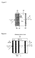
- A trim retarder compensates for residual retardation of the micro-display imager panel in a dark (OFF) state. Unlike typical birefringent waveplates providing ¼λ or ½λ retardation, a typical A-plate trim retarder provides between 1 nm and 50 nm of in-plane retardance. The primary benefit of introducing a trim retarder into a display system is to enhance image contrast, while not significantly degrading the ON-state brightness. In conventional LCOS and xLCD display systems, illustrated in Figures 1a and 1b, respectively, one or more trim retarders 2 are positioned adjacent to imager panels 3, typically less than an inch diagonal, for receiving a cone of light 4, typically with a cone illumination of ±12°, from a polarization beam splitter 5.
- Conventional thermotropic liquid crystals in reflective LCOS imager panels are either twisted nematic, e.g. 45° twist (45TN), or vertically-aligned nematic (VAN-mode), which get switched (or relaxed) to near homeotropic orientation. Other LC-modes in reflective LCOS and transmissive xLCD, i.e. bend-aligned nematic or pi-cell, also require trim retarders, if the LC-technology employs a dark-state director orientation near the homeotropic alignment. A VAN-mode cell on a reflective substrate is functionally equivalent to a pi-cell in transmission mode, i.e. both operate as electrically controllable birefringence for gray-scale with viewing angle symmetry about an axis orthogonal to the LC tilt-plane.
- In homeotropic alignment the LC uniaxial positive molecules are oriented normal to the device plane. The dark-state may be a switched state or a relaxed state, depending on LC modes. In most applications, a true homeotropic orientation in the dark state is not suitable, i.e. a pre-tilt is required to provide consistent and faster switching behavior. Moreover, true homeotropic orientation in the dark state may not be available due to a lack of high voltage supplies in 45TN panels, or due to boundary LC layers being anchored by alignment surface effects. As a consequence, the display panels exhibit both an in-plane and an out-of-plane residual retardation component, i.e. A-plate and C-plate components, respectively. Due to the use of positive-only uniaxial LC in LCD panels, the c-plate component is always positive, thereby adding to the net panel retardance at off-axis illumination.
- In typical polarization-based light engine architectures, the imager panel illumination lens has a reasonably small focal ratio (f/#), i.e. focal length/iris diameter, in order to provide for adequate light throughput. A typical f/# is 2.5 for an inch diagonal imager panel size and approximately ±12° cone angles in air. Accounting for the imager panel and the light engine characteristics, the residual retardation compensation can be broadly divided into two steps: first the in-plane retardation (IPR) component of the imager panel is negated by aligning an A-plate component with the optic axes of the imager panel (also c-axes) at 90° relative azimuth, and then improving the field of view by removing the imager out-of-plane retardance (OPR) with a negative c-plate (NCP) retarder component. Note that the optic axes may deviate slightly from the nominal crossed orientations due to the mismatch in the IPR of imager panel and the trim retarder.
- IPR compensation is almost always the primary step due to the lack of true homeotropic LC orientation. There is quite a mismatch between the relative contribution of the imager IPR and OPR to the overall net retardation under a cone illumination. As an example, the VAN-mode panel is aligned with an 80° to 89°oblique-tilt (typically 80° to 83°). The effective e-wave indices of refraction parallel and orthogonal to the device plane are given by the following expressions obtained from uniaxial index ellipsoid formula:
- With reference to Figure 3, which illustrates a conventional two-layer A/C-plate retarder model, the IPR component falls off as a function of cos(o), and the OPR component increases as a function of sin2(o)cos(o), where o is the refractive angle for the o-ray in the birefringent medium. These approximations are valid for a limited cone angle, e.g. up to ±30° in air. For a limited cone angle of ±12°, the roll-off effect on IPR is negligible; however, the net retardation contribution from the OPR is approximately,
- Assuming the average net retardance contributions from the OPR over 0° to 12° is 1%, then from the average multiples (γ) of intrinsic OPR to IPR values, the contributions of OPR to the effective retardations are given by,
- The effect of OPR at angles of incidence of less than 12° is only a fraction of the corresponding IPR retardation. These typical retardation components for VAN and 45TN-mode illustrate the critical need to first compensate for the IPR, and then improve the field of view properties of the display. It also suggests that it is paramount to compensate for the OPR in a VAN-mode panel, whereas a 45TN-mode panel has much less to gain from NCP compensation.
- An in-plane retardation component can be fabricated using the LCP/LPP technology, configured as an A-plate (planar LC director alignment) or an O-plate (oblique LC director alignment), as disclosed in copending patent applications 60/529,315 filed December 11, 2003; 60/587,924 filed July 14, 2004; and 60/589,167 filed July 19, 2004, which are incorporated herein by reference.
- In order to introduce a negative C-plate component, with the c-axis of the LC medium perpendicular to the device plane, an averaging effect of tight-pitch cholesteric LC has been proposed. For the cholesteric negative c-plate to work, the helical pitch LC medium must be shorter than the shortest wavelength in the visible wavelength range, i.e. a pitch value of 250 nm. Unfortunately, the use of cholesterics with in-plane LC director alignment may present unwanted crossed polarization leakage into an LCOS projection system, due to the high intrinsic material birefringence involved.
- Alternatively, in the area of crystal waveplates, a pseudo-zero order waveplate retarder can be fabricated by crossing optic axes of two birefringent plates. The individual layers may be positive, e.g. single-crystal quartz, or negative, e.g. Calcite, birefringence. This arrangement can also used for fabricating achromatic waveplates utilizing two waveplate elements with appropriate dispersion profiles, i.e. single-crystal quartz and magnesium fluoride combinations.
- United States Patent No. 5,196,953 issued to Yeh et al on March 23, 1993 discloses a transmissive LCD device incorporating dielectric form birefringence compensator in which the LCD is compensated by creating the conditions:
- Conventional antireflection coating designs, such as those disclosed in United States Patents Nos. 2,478,385 issued August 9, 1949 in the name of Gaiser, 3,185,020 issue May 25, 1965 in the name of Thelen, and 3,604,784 issued September 14, 1971 in the name of Louderback et al, are comprised of three layers, which cause destructive interference between reflected and refracted light within a given wavelength band defined by a center wavelength. The first layer has an optical thickness of a quarter wavelength of the center wavelength and a low refractive index, the second layer has an optical thickness of a half wavelength of the center wavelength and a high refractive index, and a third layer has an optical thickness of a quarter wavelength of the center wavelength and a medium refractive index, together forming a QHQ AR structure.
- Further advancements in antireflection coatings, which are disclosed in United States Patents Nos. 3,463,574 issued August 26, 1969 to Bastien et al, 3,565,509 issued February 23, 1971 to Sulzbach, 3,781,090 issued December 25, 1973 to Sumita, 3,799,653 issued March 26, 1974 to Ikeda, 3,936,136 issued February 3, 1976 to Ikeda et al, 4,313,647 issued February 2, 1982 to Takazawa, and 4,666,250 issued May 19, 1987 to Southwell et al relate to multi-layer antireflection coatings and the use of Herpin equivalents to design multi-layer structures with the desired index of refraction.
- An object of the present invention is to overcome the shortcomings of the prior art by providing a predictable and environmentally stable optical trim retarder for both in-plane and out-of-plane residual retardation components in transmissive, e.g. xLCD, and reflective, e.g. LCoS, image panels.
- This object is achieved by a polarization controlling device according to claim 1 and in a liquid crystal on silicon display panel assembly according to claim 17. The dependent claims define respective preferred or advantageous embodiments.
- Accordingly, the present invention relates to a polarization controlling device for providing a desired amount of phase delay to compensate for a predetermined amount of out of plane retardance between 10 nm and 1000 nm in a liquid crystal (LC) display panel, which has out of plane ordinary and extraordinary indices of refraction, comprising:
- a substrate having a refractive index;
- a form birefringent multi-layer dielectric (FB) stack disposed on the substrate including a first plurality of layers having a first refractive index and a first optical thickness; and a second plurality of layers having a second refractive index and a second optical thickness, interleaved with the first plurality of layers, defining effective out of plane ordinary and extraordinary indices of refraction; and
- first and second anti-reflection (AR) coatings at interfaces between ambient atmosphere and the device for decreasing the amount of reflection therefrom; wherein the first and second optical thicknesses are between 1/120 and 1/16 of the center wavelength resulting in a one-dimensional grating structure forming a -C plate for compensating out of plane retardances from the LC panel and from the AR coatings; and
-
- The invention will be described in greater detail with reference to the accompanying drawings which represent preferred embodiments thereof, wherein:
- Figure 1a is a side view of a conventional LCoS display panel assembly;
- Figure 1b is a side view of a conventional transmissive LC display panel assembly;
- Figure 2 is a conventional VAN-mode LC decomposed into in-plane and out-of-plane retardation components;
- Figure 3 is side view of a conventional A/C plate trim retarder;
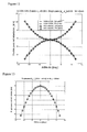
- Figure 4a is a plot of index of refraction vs n1 duty cycle estimated with 0th order EMT expressions, assuming n1=1.46 and n2=2.2;
- Figure 4b is a plot of Δn vs n1 duty cycle estimated with 0th order EMT expressions, assuming n1=1.46 and n2=2.2;;
- Figure 5 illustrates a stand-alone negative c plate (NCP) with a single FBAR stack according to the present invention;
- Figure 6 illustrates an FB coating of Fig. 5;
- Figure 7 is a plot of a single pass NCP retardation dispersion profile, as reference to a standard negative uniaxial medium;
- Figure 8 is a plot of a net retardation profile vs angle of incidence in air;
- Figure 9a is an extraordinary index of refraction profile of a conventional uniaxial material used in a dual layer A/C retarder model;
- Figure 9b is an ordinary index of refraction profile of a conventional uniaxial material used in a dual layer A/C retarder model;
- Figure 9c is a birefringence dispersion profile of a conventional uniaxial material used in a dual layer A/C retarder model;
- Figure 10 is a calculated retardation profile vs angle of incidence at an air/aluminum reflector interface;
- Figure 11 illustrates double refraction in a FBAR stack;
- Figure 12 are net retardation profiles along and orthogonal to the tilt plane of a VAN-mode LCoS panel;
- Figure 13 is a net retardation profile of an FBAR stack vs angle of incidence;
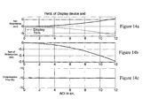
- Figure 14a shows the net retardation variations of a positive and a negative c-plate element with air angles of incidence;
- Figure 14b denotes the sum of net retardations of a positive and a negative c-plate element with air angles of incidence;
- Figure 14c presents the error of compensation as a fraction of the positive c-plate retardance when the Δnd products of the positive and negative c-plate elements are matched.
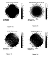
- Figure 15a is a conoscopic crossed polarization leakage profile of an LCOS device compensated with a trim retarder without an NCP element;
- Figure 15b is a conoscopic residual retardance profile of an LCOS device compensated with a trim retarder without an NCP element;
- Figure 15c is a conoscopic mode retardance profile of an A-plate trim retarder with its slow axis aligned at 135°;
- Figure 15d is a conoscopic mode retardance profile of an O-plate LCOS device with its slow axis aligned at 45°;
- Figure 16a is a conoscopic leakage profile of a compensated device according to the present invention;
- Figure 16b is a conoscopic residual retardance profile of a compensated device according to the present invention;
- Figure 16c is a conoscopic mode retardance profile of a trim retarder according to the present invention;
- Figure 16d is a conoscopic mode retardance profile of an LCoS panel;
- Figure 17 illustrates the orientations of positive tilt sense for reflection viewing of a compensated device;
- Figure 18a is a conoscopic leakage profile of a compensated device according to the present invention;
- Figure 18b is a conoscopic residual retardance profile of a compensated device according to the present invention;
- Figure 18c is a conoscopic mode retardance profile of a trim retarder according to the present invention;
- Figure 18d is a conoscopic mode retardance profile of an LCoS panel;
- Figure 19 illustrates a generic relationship between A-plate components of a trim retarder and an LCoS and the system P-polarizer and S-analyzer;
- Figure 20a is a conoscopic leakage profile of a compensated device according to the present invention;
- Figure 20b is a conoscopic residual retardance profile of a compensated device according to the present invention;
- Figure 20c is a conoscopic mode retardance profile of a trim retarder according to the present invention;
- Figure 20d is a conoscopic mode retardance profile of an LCoS panel;
- Figure 21 is a conoscopic slow-axis profile of the residual retardation in a compensated device according to the present invention;
- Figure 22 is a plot of contrast vs FBAR equivalent -C retardation for various trim retarder designs;
- Figure 23 is a schematic representation of an FBAR stack with the form birefringence stack integrated into the AR coating;
- Figure 24 is a schematic representation of another embodiment of an FBAR stack with the form birefringence stack integrated into the AR coating;
- Figure 25a illustrates a refractive index profile for an FBAR stack with the form birefringence stack integrated into the AR coating;
- Figure 25b illustrates a refractive index profile for a standard FB stack;
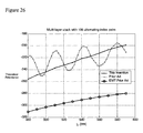
- Figure 26 is a plot of retardance vs wavelength for conventional -C plate trim retarders and -C plate trim retarders according to the present invention;
- Figure 27 is a side view of an alternative embodiment of the present invention including two FBAR stacks;
- Figure 28 is a side view of an alternative embodiment of the present invention including an FBAR stack and an a-plate on opposite sides of a substrate;
- Figure 29 is a side view of an alternative embodiment of the present invention including an FEAR stack and an a-plate on the same side of a substrate;
- Figure 30 is a side view of an alternative embodiment of the present invention including an FBAR stack and an a-plate on separate substrates laminated together;
- Figure 31 is a side view of an alternative embodiment of the present invention including two FBAR stacks and an a-plate on separate substrates laminated together;
- Figure 32 is a side view of an alternative embodiment of the present invention including one FBAR stack and two a-plates on separate substrates laminated together;
- Figure 33 is a side view of an alternative embodiment of the present invention including two FBAR stacks and two a-plates on separate substrates laminated together;
- Figure 34 is a side view of a three layered polymeric retarder having one of the layers with an in-plane retarder axis lying normal to the plane of the drawing;
- Figure 35 is a side view of an alternative embodiment of the present invention including an FBAR stack and two crystal plates with crossed c-axes; and
- Figure 36 is a side view of an alternative embodiment of the present invention including an FBAR stack integrated with the LC display panel.
-
- The present invention relates to the use of dielectric coatings with form birefringence, either as a stand-alone device or integrated with an in-plane retarder, to minimize the leakage intensity of an imager panel within limited cone angles, e.g. up to ±12°, through a pair of crossed polarizers. If the periodic optical isotropic layers are larger than the molecular lengths, but are only a fraction of the operational wavelengths, anisotropy arises from the structure, whereby the c-axis of the negative uniaxial equivalent medium lies in the direction of layer stratification, i.e. parallel to the device normal. The extraordinary and ordinary indices of refraction are given by the 0th order equivalent medium theory (EMT) to be:
- Nonetheless, the effects of taking the ratio of materials (n1 , n2) on the overall effective birefringence can be included in numerical 2x2 matrix computations for dielectric thin films.
- For example: taking Silica (n1=1.46) and Tantala (n2=2.20) dielectric coating materials in a sputtered coating, the resultant ne and no indices, as well as the birefringence (Δn = ne - no ), are estimated with the zeroth order EMT expressions (3) and (4) above. The relevant ne, no and Δn values are plotted in Figures 4a and 4b, respectively. The largest Δn can be realized by choosing a near 50:50 ratio, i.e. a near 50% duty cycle, of the two material layer thickness, at which point no =1.87 and ne = 1.72, giving a Δn of -0.15. The form birefringence stack is likely to present an effective refractive index that is a mismatch to air, the glass substrates or subsequent dielectric layers. Consequently, the form birefringence (FB) stack has to be immersed in anti-reflection (AR) coatings on both sides, thereby forming a Form Birefringence Anti-Reflection (FBAR) stack.
- The FBAR dielectric stack may be used as a stand-alone NCP compensator in a polarization-based projection system, or in combination with other discrete IPR compensators. A stand-alone FBAR trim retarder, illustrated in Figure 5, includes a plane-parallel glass plate substrate 100, approximately 1 mm thick, and a series of alternating low and high index dielectric layers, e.g. 50 to 110 layers of each, defining a form birefringence coating 101, disposed on one side of the glass substrate 100. In order to reduce material interface reflections, AR coating layers 102 are added at the air/form birefringence coating interface, AR coating layers 103 are added at the form birefringence coating/glass substrate interface, and AR coating layers 104 are added at the glass substrate/air interface. An AR coating is any dielectric or polymeric stack serving as refractive index matching layers at an interface with an abrupt index change. The multi-layer stack of low and high index dielectric layers is composed of a plurality of layers with at least two materials, one of which has a first index of refraction and another of which has a second index of refraction. The multi-layer stack may have equal or unequal number of layers for each of the two or more distinct index materials. The multi-layer stack may consist of more than one periodic multi-layer stack, interspersed by other functional dielectric designs therebetween. The AR coatings themselves provide an additional out-of-plane retardance component, which must be factored in when the overall retardance and phase difference of the FBAR is being manufactured.
- With reference to Figure 6, the form birefringent multi-layer dielectric stack 101 includes a first plurality of layers 1031, each having a first refractive index n1 and a first layer thickness d1 alternating with a second plurality of layers 1032, each having a second refractive index n2 and a second layer thickness d2. When the layer thickness is a fraction (e.g. 1/16 to 1/64) of the operating wavelength (e.g. λ=550 nm), a one-dimensional grating structure results and birefringence property of the coating stack arises. Stand-alone NCP and AP/NCP trim retarders, similar to the structures depicted in Figure 5, have been evaluated using variable-angle spectro-ellipsometry (VASE) data collection and analysis, and the resultant retardation profile versus AOI in air was then fitted to the standard dual-layer retarder model. The stand-alone NCP retarder results are plotted in Figure 7, in which the standard uniaxial material reference has no and ne indices of 1.65 and 1.50, respectively, at λ=550 nm. The difference between theoretical and experimental results, fitted to the two-layer retarder model, is only about 10 nm throughout the band. The dielectric stack fabrication involving very thin layers (< 20nm) had been implemented with a very stable coating platform. An example of the net retardation profile versus AOI in air is shown in Figure 8, for a trim retarder incorporating an O-plate IPR layer and FBAR NCP stack. Owing to the O-plate tilt, the single-pass net retardation profile varies according to the viewing azimuth plane. VASE data had been collected along the two principal, slow and fast axes, planes. Along the slow axis plane (also the tilt plane), the retarder shows a characteristic o-plate single-pass profile, as well as the decrease in net retardation with AOI, as a result of the FBAR NCP element.
- The layer thickness of the dielectric coating materials n1 and n2 are chosen to create a suitably large birefringence, such that the dispersion across a band of wavelength is minimized or tailored to system requirements. The resultant effective no and ne refractive indices may not be suitable for direct contact with the other optical media, e.g. air, substrate; however, as stated above, the remedy for index mismatches is to add AR layers on either side of the multi-layer stack. According to the present invention the effective off-axis effects of the imager panel are equated with those of the trim retarder. The angular spread of off-axis rays in a high index FEAR equivalent medium, e.g. no and ne values of approximately 2.0, is less than the corresponding values typically found in an LC medium, e.g. no and ne values of approximately 1.5 to 1.65. Therefore, unlike the prior art, the birefringence-layer length product, i.e. And, of the FBAR stack has to be appreciably larger than the corresponding c-plate And of the imager panel LC-layer to obtain the same amount of phase difference. According to the present invention, FBAR c-plate retardation effects are benchmarked against a reference negative uniaxial medium having standardized indices: no =1.65 and ne =1.50 @ λ=550 nm, using a dual-layer retarder model as shown in Figure 3. Similarly, the off-axis effects of the imager panel are benchmarked against a positive uniaxial medium having no =1.50 and ne =1.65. The reference birefringent media may also incorporate index and birefringence dispersions across the wavelength range of interest, such as plotted in Figures 9a to 9c. Referencing the panel retardation to a standard uniaxial medium has the added advantage that the retardation is a measurable macroscopic effect of the layer, without the need to obtain panel LC material constants. The measured retardance of a reflective LCOS also includes the off-axis effects of a metallic reflector. The calculated retardation profile of an Air/Aluminum reflector interface is shown in Figure 10. The aluminum substrate had a complex index of (0.985-6.67i) @ λ=550 nm, and the fitted c-plate retardance is approximately 66 nm on reflection. In a typical LCOS construction, the aluminum reflector is immersed in a higher index medium, such as LC or an LC alignment layer. Consequently, the effective angles of rays impacting on the aluminum interface are reduced. The off-axis effect of the metal reflector at the silicon backplane, such as aluminum, is greatly reduced.
- With reference to Figure 11, the birefringence of the FBAR stack arises as the following. For an input incidence consisting of 's' and 'p' polarized light, the 's' polarized light sees the 'no ' index whereas the 'p' polarized light sees an effective index, which is a function of the 'no ' and 'ne ' indices. The 's' polarized light component propagates as the ordinary wave, and the 'p' polarized light component propagates as the extraordinary wave in the FBAR equivalent uniaxial c-plate. The eigen-modes and eigen-indices of the two waves are given by the expressions as follows:
- An example of a retardation compensation approach according to the present invention is as follows: the retardation profiles of an 83° tilt VAN-mode LCOS device and an FBAR trim retarder element are fitted with an A/C or A/-C dual-layer equivalent retarder model. The LCOS has an LC layer between a Coming 1737F cover glass and an Aluminum substrate. The glass plate has a nominal index of refraction of 1.52 at λ =550nm. The LC-layer uses the standard uniaxial positive medium of ne=1.65 and no =1.50 at λ =550nm, with a thickness of approximately 2.35µm to provide for about 4.5 nm of in-plane retardance (single pass). The air/glass interface has a nominal broad-band AR design. The fitted results, along and orthogonal to the VAN-mode tilt plane, are plotted in Figure 12. The equivalent retarder model includes an a-plate and a positive c-plate (PCP) layer, both utilizing the standard uniaxial material indices, sandwiched between two AR-coated Corning 1737F glass plates. The LCOS device model has 83° uniform LC director tilt and an intrinsic LC birefringence of 0.15. The LCOS device is fitted to be equivalent to an A/C retarder having 4.5 nm and 340 nm of in-plane and out-of-plane retardance, respectively. The in-plane retardance is the net retardance of the model at normal incidence. The 4x4-matrix computation employed here, includes interference and reflections at the layer interfaces. In order to compensate for the LCOS retardation components of 4.5/340 nm, prior art teaches a trim retarder having an in-plane component of ∼4.5 nm and an out-of-plane component of approximately -340 nm. The in-plane component is obtained by using either an a-plate or an o-plate birefringent element, having its slow axis aligned orthogonal to the VAN-LCOS tilt plane, thus forming a crossed-axes pair. The out-of-plane component of -340 nm can be obtained, for example, with an FBAR element according to the present invention. The FBAR element may be a stand-alone compensator or form an integral part of a full-function trim retarder. Other negative c-plate elements, which shall be disclosed in the following, may also replace the FBAR functions. In addition, it shall be shown that the prior-art teachings of A/-C-plate trim retarder design do not result in optimal compensation.
- As an example, an FBAR element in the form of a stand-alone compensator, of the type shown in Figure 5, uses 71 pairs of Tantala and Silica layers, having nominal indices of 2.20 and 1.46 at λ=550 nm, respectively. A large difference, e.g. greater than .5 and preferably greater than 0.7, between n1 and n2 is selected to maximize the birefringence and minimize the thickness of the coating. AR layers are added to reduce reflections between the periodic thin layer stack with air and Corning 1737F glass on either side. The reverse side of the glass is also AR coated. The retardance profile of the FBAR stack, evaluated over the same ±12° AOI range in air, is plotted in Figure 13. Note that within the cone angles, the FBAR stack provides for a net retardation of approximately -6.3 nm to 0 nm single pass, whereas the VAN-mode LCOS gives rise to approximately 5.7 nm to 0 net retardation, single pass. In terms of the birefringence of the effective indices, the VAN-mode LCOS and the FBAR stack have a Δnd product of:
- In which Δnc is the effective out-of-plane birefringence: in the case of VAN-mode o-plate, it is the uniaxial projection onto the z-axis; in the case of the FEAR stack, it is the difference of effective (no , ne ) indices. Accordingly, because the refractive indices n1 and n2, the resultant effective out of plane refractive indices no and ne are larger than the corresponding refractive indices of the LCoS panel, which causes the angle spread for an e-wave and an o-wave, and the actual phase difference in the FBAR stack to be less than that in the LCoS panel. Hence, the phase anisotropy is reduced and the thickness of the FBAR stack has to be increase to get the required phase difference at the exit thereof.
- Evidently, the aforementioned FBAR example, providing for -415 nm c-plate retardance in terms EMT effective indices or -340 nm in terms of the standard uniaxial material model, does not provide for an adequate off-axis compensation of the 4.5/340 nm VAN-mode LCOS (IPR compensated for separately). From the expressions of eq. (5) and (6), the net retardances for a given off-axis ray, where in the LCOS device, {no,ne} material set is assigned {1.50, 1.65} @ λ=550 nm and in the trim retarder device, {no,ne} material set is assigned {1.65, 1.50} @ λ =550 nm, does not sum up to zero. The general angular profiles of the net retardances in the positive and negative C-plate elements, with matched lower and higher eigen-indices are shown in Figures 14a to 14c. With this matched index condition, the sum of positive and negative net retardances, at any given angle of incidence, deviates by approximately 1-no (LCos)/n o(FBAR) or -10% as a fraction of the LCOS c-plate compensation target.
- Accordingly, the proper -C-plate component in the trim retarder, for removing the residual retardance of a 4.5/340nm VAN-mode LCOS, should be approximately -340/(no (FBAR)/no (LCoS)) = -340/1.1 or - 310nm. Without an NCP element in the trim retarder compensator, the compensated LCOS device has ring-like (more precisely oval-shaped) net retardance profile, as shown for ±12° cone angles in Figure 15b. The associated conoscopic crossed-polarization leakage profile is depicted in Figure 15a - the so-called isogyre cross is evident along the input and exit polarizer directions where only a single mode of propagation exists. The cone-average contrast of this compensated device (assuming an On-stage intensity of 100%) is no better than 2000:1. The conoscopic A-plate retardance, with its slow axis aligned at 135° is shown in Figure 15c, depicting a weak variation with polar angles. The mode retardance profile of the O-plate birefringent layer in the VAN-mode LCOS, as shown in Figure 15d, has 180° symmetry in double-passing. The combination of an A-plate trim retarder and an O-plate LCOS device, wherein the residual a-plate is completely removed, results in the oval-shaped conoscopic net retardance profile. By introducing an appropriate amount of -C retardance component (∼-310nm in this case), the field of view is increased, as evidenced in the conoscopic leakage plot of Figure 16a. The NCP element is implemented with an FBAR design including 48 pairs of 19nmH/21nmL, where H and L are Tantala and Silica of 2.3 and 1.5 refractive indices, respectively. The conoscopic leakage and net retardance (Figure 16b) profiles are uniformly low, with slight ring-like perturbation. This is evidence that an A/-C plate compensator is suitable for complete residual retardance removal of a VAN-mode LCOS having a very high tilt (83° in this example). The NCP element in the trim retarder is radially symmetric, whereas the PCP retardance of the high-tilt VAN-mode LCOS is close to being radially symmetric. The individual conoscopic mode retardance profiles of the trim retarder and the LCOS stages (Figure 16c and 16d) reveal closely matched mode retardance at any given ray angle.
- A problem with the above A/-C plate trim retarder design is that, although the forward compensation contrast is very high (> 25k: 1), the reflection off the front-face of the trim retarder impose an overall contrast limit of ∼2000:1 even for a low-value 4.5nm A-plate retarder. There are various ways to reduce the reflection, i.e. reducing the Δn of the LCP layer in the A plate, as disclosed in copending patent applications 60/529,315 filed December 11, 2003; 60/587,924 filed July 14, 2004; and 60/589,167 filed July 19, 2004. An alternate scheme is to employ an O-plate retarder medium to realize the A-plate component. It is well-known that an optimally compensated LC-device with a tilt-plane requires that all four quadrants of the viewing cone encounter compatible out-of-plane tilt of a uniaxial medium [H. Seiberle, K. Schmitt and M. Schadt, "Multidomain LCDs and Complex Optical Retarders Generated by Photo-alignment," Proc. Eurodisplays '99, pp. 6-9, September, 1999]. With a two-stage compensator-LCOS device, oriented substantially parallel to each other in double-pass transmission, this four-domain structure can be easily synthesized by crossing the tilt-plane of an O-plate trim retarder with the tilt-plane of VAN-mode LCOS. The orientations of positive tilt sense for reflection viewing of the compensated device is shown by the diagram in Figure 17, for the nominal case of matching a-plate retardance components of LCOS and trim retarder. The tilt sense of the first and second passes of LCOS and trim retarder could be offset by 90° or 180°, as long as they interleave by a nominal 90° and populate all four quadrants of the viewing cone.
- A set of calculated compensation results for a 65° trim retarder O-plate and the abovementioned 83° VAN-mode LCOS are shown in Figures 18a to 18d. The trim retarder out-of-plane tilt of 65° is a practical, average tilt of splayed O-plate LCP retarder; whereas the tilt angle of the VAN-mode LCOS is likely to be very high (> 80°). Even in this case of unmatched LCOS and trim retarder out-of-plane tilts, the compensated device has a very small degradation, in comparison to the previous case of A/-C trim retarder compensator. At 65° tilt, the amount of C-plate retardance induced by the LCP layer is about 22 run (5x of A-plate component), which requires ∼-20 nm of NCP compensation. The FBAR stack in this case includes 51 pairs of 19nmH/21nmL, giving a net trim retarder c-plate component of ∼-310nm. With a 65° LCP tilt, the reflection contrast limit is pushed out to several tens of thousands to one. It can be seen that the individual conoscopic mode retardance profiles of the trim retarder and the LCOS stages (Figure 18c and 18d) are still closely matched over the entire ±12° viewing cone.
- Due to the manufacturing tolerances of the LCOS and the trim retarder, the values of in-plane retardance of both elements may vary by tens of percentages from part to part. A convenient technique to ensure adequate IPR compensation is to always utilize a substantially higher in-plane value trim retarder to pair up with any given LCOS panel, where the trim retarder is 'clocked-in' by rotating its azimuth orientation away from the crossed-axes arrangement. A generic relationship between the a-plate components of trim retarder and LCOS and the system p-polarizer (parallel to x-axis) and s-analyzer (parallel to y-axis) is shown in Figure 19. The c-plate component is rotationally invariant, if realized by an FBAR stack or a true negative uniaxial plate. When the trim retarder is under compensating the LCOS, there is only one optimal trim orientation (for an LCOS axis at 135° + , || < 22.5°). The trim retarder axis is not crossed with the LCOS axis, rather the trim retarder azimuth lines up at 45°, bisecting the 'p' and 's' planes. When the trim retarder value just matches the LCOS retardation, two azimuth solutions emerge: the first aligns the trim at crossed-axes with the LCOS whereas the second has the trim retarder and LCOS at mirrored orientations with respect to the y-axis, i.e. an over-clocking angle of 2. When the LCOS axis lines up with ±45°, the two solutions merge into one. In the case of over-compensation, the two trim retarder azimuth solutions bisect the 45° directions. The angle offsets (either δ or -(2+δ) for solutions #1 and #2, respectively) increase with the retardation mismatches. The over-clocking angle, δ, is approximately given by, cos-1[Γa(TR)/Γa(LCOS)]/2, assuming approximately COS2 (δ) retardance projection in the intended azimuth.
- An example of a 4.5/340nm VAN-mode LCOS device, compensated with a 6.5/-310nm mismatched-AP O/-C plate trim retarder is shown by the results in Figures 20a to 20d. Due to the increased A-plate component of the trim retarder, the associated increased in PCP (∼5*6.5 nm or 33nm) in the trim retarder requires an additional -30 nm of NCP in the FBAR stack. An FBAR stack including 53 pairs of 19nmH/21nmL is used. The overall conoscopic leakage profile is uniform as shown in plot (a). However, the net retardance of any given ray traversing the trim retarder/LCOS in double-pass is no longer near zero. In this example, almost 9.5 nm of net retardance remains for any given ray, with the TR slow axis clocked an additional ∼23° from the crossed-axes alignment to LCOS slow axis. Fortunately, the fast/slow axes of this net retardance are very closely aligned to the system 'p' and 's' directions, resulting in negligible birefringence effects (Figure 21). The conoscopic mode retardance of the 6.5/-310 nm trim is not a mere rotated version of the previous 4.5/-310 nm O/-C trim retarder (compare Figures 20c and 18c). The effects of non-rotationally symmetric PCP (due to LCP O-plate) and the rotationally symmetric NCP (due to FBAR stack) combined to give a mode retardance profile as Figure 20c. The clocked trim retarder/LCOS retarder pair then produces magnitude and axis orientation maps as given in Figures 20(b) and 21.
- Accordingly, the out-of-plane component of the VAN-mode LCOS is optimally compensated for by the FBAR stack, assuming there is no other birefringent element in the display system giving rise to in-plane and out-of-plane retardation components. An optimal trim retarder solution requires a computer optimization and/or with experimental iterations of the complete polarization-based projection system including the trim retarder, the LCOS panel, polarizers, analyzers, polarization beam splitters and any other polarization sensitive elements.
- With just the VAN-mode LCOS and an O/-C plate trim retarder in an optical system, the number of periodic H/L thin-layer pairs has been varied in a fine NCP granularity manner in order to probe the sensitivity of the compensated paired devices with respect to the NCP retardance targeting. The results of A/-C and O/-C plate trim retarder designs for the same 4.5/340nm VAN-mode LCOS are shown in Figure 22 (the case of mismatched AP compensation is denoted by O/-C*). It is clear that the forward compensation contrast is as good for any of the three examples. In practice the very high forward compensation contrast (∼25k:1) is set back by a slew of leakage mechanisms in a display system, collectively lumped as the baseline contrast of the optical system. It is typical to achieve between 6k:1 and 10k:1 system baseline contrast for a wire-grid PBS based projection system. In this case, the sensitivity of the C-plate retardance variation is mitigated and an overall system contrast greater than 4000:1 can be obtained (parallel contributions of 1/6k and 1/25k and at least 50k:1 reflection contrast).
- Accordingly, in the four calculation examples above, a step-by-step trim retarder compensator design has been presented. First, a prior-art A-plate-only trim retarder, with an exactly matched a-plate retardance to that of the VAN-mode LCOS is presented. Second, the lack of field of view is compensated by incorporating a novel FBAR thin-film stack into the trim retarder. Third, the lack of reflection contrast is overcome by utilizing an effectively low in-plane birefringence retarder design. The practical compensation match-up where the trim retarder a-plate component is substantially larger than the corresponding component of the LCOS is illustrated in the fourth example. The last example represents the preferred embodiment for working with typical manufacturing tolerances.
- Accordingly, as evidenced by the aforementioned examples is: a) there is no need to deduce the actual layer thickness and the associated (ne, no ) indices of the LCOS LC layer; b) there is no need to deduce the optical constant of the metal reflector at the silicon backplane; c) the c-plate Δnd product of LCOS is in general unequal in magnitude to the c-plate Δnd product of the FBAR negative c-plate, or any negative c-plate element in the trim retarder; d) it is not desirable, nor necessary, to equate the effective (ne, no ) index set of the LCOS device and that of the FBAR stack, i.e. ne (LCOS) = no (NCP) and no (LCOS) = ne (NCP) conditions are redundant; and e) it is not desirable, nor necessary, to equate the actual physical lengths of the LCOS device and that of the FBAR stack, i.e. d(LCOS) = d(NCP) condition is redundant.
- A compensated display system requires optimal c-plate element that equates the off-axis effects of the LCOS device and the compensator device. Although not shown in examples here, the design approach is equally applicable to other LCOS modes of operations, such as TN. It is expected that the overall compensated TN device contrast will be substantially lower than the VAN-mode case, principally because the larger in-plane retardance component (∼20nm for TN vs. < 5nm for VAN-mode) entails a lower reflection contrast and a different Off-state LC director distribution (with lower PCP/AP ratio than VAN-mode) gives a higher azimuthal dependence of the crossed-polarization leakage cone.
- With reference to Figure 23, rather than depositing conventional antireflection (AR) coatings at the air/FB interface and the substrate/FB interface, an embodiment of the present invention incorporates the form birefringent stack 151 into the AR coating, generally indicated at 152, as a first quarter wave structure 153 adjacent to a substrate 154. The form birefringent stack 151 has an effective refractive index higher than the substrate 154. A half wave structure 156 with a high refractive index, i.e. greater than the effective refractive index, is deposited on the first quarter wave structure 153, and a second quarter wave structure 157 with a low refractive index, i.e. less than the effective refractive index and the refractive index of the substrate, is deposited on the half wave structure 156 to complete a QHQ AR coating 152.
- Unfortunately, the form birefringent stack 151 has a phase thickness about twenty to fifty times larger than a single quarter wave layer, which can also vary by about 5 to 10 quarter waves over the range of wavelengths, resulting in a narrowing of the wavelength range in which the AR coating is effective. Accordingly, additional layers in the first quarter wave, the half wave and/or the second quarter wave structures 153, 156, and 157, respectively, are required to match the rapidly changing phase of the form birefringent stack 151. The second quarter wave structure 157 can be replaced with a symmetric three layer combination, e.g. herpin equivalent, with alternating high and low index material resulting in an equivalent index, but potentially three times the phase thickness. The half wave structure 156 can be replaced with one or more full wave or multiple half wave structures. Additional layers may also be required in the first quarter wave structure 153 to add onto one or both sides of the form birefringent stack to achieve the desired indices and phase thickness.
- If the form birefringent stack has 106 layers of high index material (nH=2..16 or higher) 10 nm wide alternating with 106 layers of low index material (nL=1.48), i.e. (5nm H - 10nm L - 5nm H)106, the equivalent index of refraction would be nE =1.846. For a typical glass substrate nS=1.52 and an ambient air atmosphere, the initial first quarter wave structure could have an index nQ1 =1.50 and a thickness of approximately 92 nm, and the initial half wave structure could have an index nHW =2.3 and a thickness of approximately 120 nm. However, to compensate for the rapidly changing phase of the form birefringent stack the half wave structure comprises one half wave and the second quarter wave structure comprises five quarterwave equivalent structures. Figure 24 indicates that the second QW structure 157, has now been split into five quarter wave structures. The five quarter wave structure, 157, the half wave structure, 156, and phase adjusting layers of the FB stack, 159, are optimized to meet the reflectance and retardance targets over the wavelength band of interest. The number of layers required depends on their physical thickness, the effective Δn and the amount of desired retardance, e.g. for layers 5nm wide with an effective Δn of 0.15 over 500 pairs to provide 1000 nm of retardance; however, only approximately 10 pairs will be required to provide 10 nm of retardance. A range between 50 and 110 pairs of high index/low index is preferred.
- Figure 25a illustrates the refractive index profile for an FBAR stack according to the present invention, compared with that of the form birefringent stack without AR coatings, illustrated in Figure 25b. Figure 26 illustrates the highly variable retardance of a conventional -C plate trim retarder (the trace marked 'Prior Art') across the visible spectrum compared with the relatively stable retardance of the trim retarder according to the present invention. ('This invention'); both sets of results are fitted to equivalent no =1.65 and ne =1.50 indices. The retardance profile, according to zeroth order EMT expressions, is plotted as the 'EMT Prior Art' trace.
- Yet another embodiment of the stand-alone NCP involves the splitting of the required retardance into two separate FBAR stacks 113 and 114, coated on opposite surfaces of a glass substrate 110, as illustrated in Figure 27. Again, AR layers 111 and 112 are provided to reduce the reflections. Alternatively the form birefringent stack could be incorporated into AR coating, as in Figure 23 and 24. Radially-symmetric C-plate retardance, such as those given by an FBAR stack, can be linearly superposed. Accordingly, a plurality of FBAR stacks, coated on multiple substrates can be cascaded in parallel, without any relative azimuth orientation constraint. Moreover, c-plate trim retarders can be cascaded on a single side of reflective imager or positioned on one or opposite sides of a transmissive imager.
- The full scope of contrast enhancement, by incorporating a trim retarder into a polarization based display system, can only be realized with both IPR and OPR compensation. An emerging trend in polymeric IPR compensation is to utilize a spin-coated LCP on an LPP alignment layer; however, the lack of negative birefringence LCP, compatible with the spin-coating process, does not allow for the full compensation of the imager at off-axis illumination. By integrating the FBAR stack with an LCP/LPP layer sequence, a full-function A-plate/negative C-plate (AP/NCP) trim retarder, which compensates for imager IPR and increases the display system field of view, results. A C component of the LCP/LPP structure is determined and factored into the final design of the FBAR stack to ensure the desired compensation is provided.
- A preferred embodiment of an AP/NCP trim retarder, incorporating a FBAR stack is illustrated in Figure 28, and includes series of alternating index layers, forming the form birefringence stack 203, bounded by index matching AR layers 201 and 202, disposed on one side of a glass substrate 200. Alternatively the form birefringent stack could be incorporated into the AR coating, as in Figure 23 and 24. On the opposite side of the glass substrate 200, a similar stack of layers 204 is constructed to provide for IPR. Alternatively, the macroscopically birefringent element 204 may be composed of an LCP/LPP layer sequence. The LCP layer or layers can be aligned with their LC directors planar or oblique with respect to the substrate (i.e., a-plate or o-plate uniaxial configuration), as long as the resultant structure has an in-plane retardation component. Ideally, the IPR element 204 is bounded by AR stacks 205 and 206 for reducing reflections. For trim retarder applications, in which polymers are not ideal, e.g. in high light flux displays systems, the IPR element may be constructed out of all dielectric materials. In this case, the FBAR structure may be coated on the opposite side of the substrate or as an additional multiple-layer dielectric coating coated onto the dielectric a-or o-plate retardation element. With reference to Figure 29, a form birefringence element 213 and an IPR element 214, which may be a positive uniaxial polymeric medium aligned with an in-plane birefringence, i.e. either o-plate or a-plate configuration, are coated on a single side of a substrate 210. The arrangement of elements 213 and 214 may be reversed to make the fabrication process easier. Preferably, the birefringence elements 213 and 214 may also be bounded by AR layers 211, 212, 215 and 216 to reduce interface reflections. The FBAR stack 213, incorporated into a full-function AP/NCP trim retarder, is used to offset any positive c-plate (PCP) retardation component from the trim retarder itself, as well as the OPR of imager panel.
- Other embodiments of AP/NCP trim retarders, incorporating a plurality of FBAR stacks and a plurality of IPR elements, are illustrated in Figures 30 to 33. These embodiments are particularly useful when more than one FBAR stack and more than one IPR element are needed, but the two retarder elements cannot be sequentially coated on one another. In Figure 30, an IPR element 300, such as an LCP on LPP structure, and an FBAR stack 301 are assembled together by way of an epoxy layer 302. The IPR element 300 is an integrated sub-assembly consisting of a glass substrate 303, AR coating layers 304a and 304b, and a birefringent medium 305. The FBAR sub-assembly 301 includes a glass substrate 306, AR coating layers 307a and 307b, and a series of alternating index #1 and index #2 dielectric layers 308. Alternatively the form birefringent stack could be incorporated into AR coating, as in Figure 23 and 24. The advantage of the laminated trim retarder structure is the ability to mix and match FBAR-coated cover-glass sub-assemblies. For example, the IPR element 300 may be a common design for the entire visible wavelength band and depending on the selected color-band of use in a projection light engine, but the FBAR sub-assembly 301 may be targeted for Red, Blue or Green designs. Due to the high dispersion of the FBAR c-plate retardation over the visible wavelength range, interchangeable FBAR sub-assemblies makes the design and assembly processes easier.
- Other variations of the non-integral AP/NCP trim retarder structure involve the lamination of IPR/FBAR sub-assembly 310 with an FBAR-coated cover glass 311 with an adhesive layer 312 therebetween, as in Figure 31. The IPR/FBAR sub-assembly 310, similar to that of Figure 28, includes a glass substrate 313 with a stack of alternating dielectric layers 315 on one side and an IPR element 316 on an opposite side. AR coatings 314a, 314b and 314c are applied at the material interfaces. The FBAR sub-assembly 311, similar to Figure 5, includes a glass substrate 317 with a stack of alternating dielectric layers 319 coated thereon. As usual AR coating 318a and 318b are applied at the material interfaces. Alternatively the form birefringent stack could be incorporated into AR coating, as in Figure 23 and 24. With reference to Figure 32, an IPR sub-assembly 320 and an IPR/FBAR sub-assembly 321 are laminated together with a suitable adhesive layer 322. The IPR sub-assembly 320 includes a glass substrate 323 coated with AR coatings 324a and 324b, and with an IPR element 325 disposed thereon. As above, the IPR/FBAR sub-assembly 321 includes a glass substrate 326 with a stack of alternating dielectric layers 328 on one side and an IPR element 329 on an opposite side. AR coatings 327a, 327b and 327c are applied at the material interfaces. Alternatively the form birefringent stack could be incorporated into AR coating, as in Figure 23 and 24. A symmetric pair of IPR/FBAR sub-assemblies 330 and 331, are illustrated in Figure 33. The first IPR/FBAR sub-assembly 330 includes a glass substrate 333 with a stack of alternating dielectric layers 335 on one side and an IPR element 336 on an opposite side. AR coatings 334a, 334b and 334c are applied at the material interfaces. Alternatively the form birefringent stack could be incorporated into AR coating, as in Figure 23 and 24. The second IPR/FBAR sub-assembly 331 includes a glass substrate 337 with a stack of alternating dielectric layers 335 on one side and an IPR element 338 on an opposite side. AR coatings 339a, 339b and 339c are applied at the material interfaces. Alternatively the form birefringent stack could be incorporated into AR coating, as in Figure 23 and 24. All the sub-assembly structures referred to above have the basic structure of a series of dielectric or polymeric layers coated on one or both sides of a glass substrate, and preferably include AR-function layers.
- It is important that a trim retarder solution for a VAN-mode and a TN-mode LCOS imager incorporates both an IPR and an NCP retardation component. If the IPR element is implemented with LCP/LPP layered structures, there is an opportunity to realize NCP functionality by crossing the slow-axis of two or more a-plate elements, or two or more o-plate elements. By crossing the principal axes, the difference between the element in-plane retardation components manifests as the net in-plane retardation; the common value of the in-plane retardation components becomes the negative c-plate component; and all positive out-of-plane retardation components sum up as the net positive c-plate retardation.
- With reference to Figure 34, a polymeric retarder 204 includes three layers of LPP material 2042, 2043 and 2044, each aligned with a thin layer of LPP material 2041. The LPP layers 2042 to 2044 may be homogenous in tilt profile, e.g. a-plates, or they may be splayed o-plates. Layers 2042 and 2043 may be constructed in a mirrored tilt fashion so as to mimic the pi-cell effect in a single-pass, thereby having an effective in-plane retarder axis lying in the plane of drawing (projection of LC director along the vertical direction). If the tilt profiles of the layers 2042 and 2043 are similar or symmetric, the net in-plane retardation component is proportional to the sum of thickness (da + db). The third LCP layer 2044 is disposed on the LCP/LPP stack, i.e. layers 2042 and 2043, but with the effective in-plane retarder axis lying normal to the plane of drawing (projection of LC director along the horizontal direction). Accordingly, if the tilt-profile has the same effective value, the net a-plate component is given by |da + db - dc|*Δn (effective in-plane). The NCP value is the smaller of (da+db) and dc, multiplied by Δn (effective in-plane); the positive c-plate component is given by (da+db+dc)* Δn (effective out-of-plane). Therefore, a multi-layer O-plate structure is inadequate to create a net NCP effect. Two or more layers of a-plate elements would have to be used to create a trim retarder that has the AP/NCP functionality requirement. Rather than using the multiple-layer o-plate structure 204, an FBAR stack, as shown in Figure 28, can be used to offset the resultant positive c-plate components.
- While the NCP given by the FBAR stack is radially symmetric, the same cannot be said about the crossed-axes a-plates or o-plate elements. Due to the presence of two in-plane retarder axes, the off-axis effects along and away from these axes are quite different. In general, it can be shown that an AP/NCP trim retarder incorporating crossed-axes a-plate elements delivers approximately half the compensation efficiency as compared to the an AP/NCP trim retarder incorporating radially-symmetric NCP, such as crystal-based negative uniaxial c-plate, FBAR stacks or bidirectionally-stretched polymeric films. Because of this lack of efficiency, pseudo-zero order crystal plates, providing a non-polymeric IPR element, may be better suited for integration with an FBAR stack. With reference to Figure 35, the difference between the widths of the two crystal plate elements 404 and 405 provides for the a-plate component. For trim retarder applications, a low pseudo-zero order is more desirable for crystal plate processing than a true zero order crystal waveplate. For example, to realize a 20 nm in-plane retardance at λ=550nm, a single-crystal quartz would have to be ∼2µm thick, however, the required in-plane retardance can also be obtained by crossing the axes of a 10µm plate and a 12µm plate, which thereby provides a -90 nm NCP component. In order to obtain a few hundred nm of NCP within the visible wavelength spectrum, an FBAR stack 402 can be added to glass substrate 400 opposite the thin crystal plates 404 and 405. For transmission at normal incidence, the FBAR stack 402 serves as a high efficiency AR coating and at off-axis transmission, the FBAR stack 402 introduces relative delays between the two eigen modes of propagation. Traditional AR coating 401a, 401b, 403a and 403b are provided at the material interfaces. Alternatively the form birefringent stack could be incorporated into AR coating, as in Figure 23 and 24.
- In high performance projection system displays, the contrast requirement could be several thousands to 1. Reflected rays from birefringent elements acquire a fraction of the net retardation due to imperfect external AR coatings. Imperfect AR coatings have detrimental effects by converting the incoming linear polarization into an orthogonal linear polarization component, which gets imaged onto the screen through a pair of crossed polarizer-analyzer settings, along with the main beam. In simple compensated micro-displays, illustrated in Figures 1a and 1b, there are at least two redundant AR-coated surfaces of the trim retarder and the display panel, each facing the other, that can be removed by making the trim retarder assembly part of the LCOS or xLCD backing/cover glass plates. An integrated trim retarder and LCOS display panel cover glass are illustrated in Figure 36. A complete AP/NCP trim retarder sub-assembly, similar to that of Figure 29, includes a FBAR stack 502 and a polymeric or dielectric IPR element 503 disposed on one side of the glass substrate 500 with suitable AR-coating layers 501a, 501b and 501c therebetween. Alternatively the form birefringent stack could be incorporated into AR coating, as in Figure 23 and 24. The glass substrate 500 forms an LC cell gap 506 with a top-level metal reflector 505, which is disposed on top of a silicon backplane (substrate) 504. The LC cell assembly is completed with alignment layers 507, e.g. polymeric or obliquely evaporated inorganic layers, and front transparent conductive electrode 508, e.g. indium tin oxide (ITO).
wherein a difference between the first and second indices of refraction is greater than 0.5 for increasing the effective indices of refraction and decreasing the width of the FB stack required.
Claims (20)
- A polarization controlling device for providing a desired amount of phase delay to compensate for a predetermined amount of out of plane retardance between 0 nm and 1000 nm, single pass, in a liquid crystal display panel, which has out of plane ordinary and extraordinary indices of refraction, comprising:wherein the first and second optical thicknesses are between 1/120 and 1/16 of the center wavelength resulting in a one-dimensional grating structure forming a -C plate for compensating out of plane retardances from the liquid crystal panel and from the anti-reflection coatings; anda substrate (100; 154; 110; 200; 210; 306; 317; 326; 337; 400; 500) having a refractive index;a form birefringent multi-layer dielectric stack (101; 151; 114; 203; 213; 308; 319; 328; 335; 402; 502) disposed on the substrate including a first plurality of layers (1031) having a first refractive index and a first optical thickness; and a second plurality of layers (1032) having a second refractive index and a second optical thickness, interleaved with the first plurality of layers, defining effective out of plane ordinary and extraordinary indices of refraction; andfirst and second anti-reflection coatings (102; 104; 152; 112; 202; 205; 211; 216; 307a, 304a; 318a, 314a; 327a, 324a; 339a; 334a) at interfaces between ambient atmosphere and the device for decreasing the amount of reflection therefrom;
wherein a difference between the first and second indices of refraction is greater than 0.5 for increasing the effective indices of refraction and decreasing the width of the dielectric stack required. - The device according to claim 1, wherein the effective indices of refraction of the form birefringent stack (101; 151; 114; 203; 213; 308; 319; 328; 335; 402; 502) are greater than corresponding indices of refraction of the liquid crystal panel, whereby the retardance of the form birefringent stack is greater than that of the liquid crystal panel to provide the desired phase delay.
- The device according to claim 1 or 2, wherein a first physical thickness of each of the first plurality of layers (1031) is substantially the same as a second physical thickness of each of the second plurality of layers (1032) for maximizing retardance.
- The device according to any one of the preceding claims, wherein the form birefringent stack (151) forms a first quarter wave structure (153)wherein the first quarter wave structure has an effective index of refraction and a rapidly changing phase over a wavelength range;
wherein the first anti-refelection coating comprises:wherein the first quarter wave structure (153), the first half wave structure (156) and the second quarter wave structure (157) form an integrated anti-reflection coating (152); anda first half wave structure(156) adjacent the first quarter wave structure (153)having an index of refraction higher than the effective index of refraction, the first half wave structure (156) including multiple layers of alternating high and low refractive index materials for at least partially compensating for the rapidly changing phase of the first quarter wave structure (153), the first half wave structure (156) contributing out of plane retardance; anda second quarter wave structure (157) adjacent the first half wave structure (156) having an index of refraction lower that the effective index of refraction, the second quarter wave structure (157) including multiple layers of alternating high and low refractive index materials for at least partially compensating for the rapidly changing phase of the first quarter wave structure (153), the second quarter wave structure (157) contributing out of plane retardance;
wherein the amount of out-of-plane retardance from the first quarter wave structure (153), the first half wave structure (153), and the second quarter wave structure (157) combine to provide the desired amount of phase delay. - The device according to any one of the preceding claims, further comprising a liquid crystal on silicon display panel (505-508) creating both in plane and out-of-plane retardance in light passing therethrough including off-axis effects of a metallic reflector; wherein the wavelength range is between 380 nm and 780 nm; wherein the form birefringent stack (502) compensates for the out of plane retardances from the liquid crystal panel (506), the anti-reflection coatings (501a, 501b, 501c) and the metal reflector (505).
- The device according to any one of the preceding claims, wherein the form birefringent stack (101; 151; 114; 203; 213; 308; 319; 328; 335; 402; 502) comprises between 10 and 500 first layers (1031), and between 10 and 500 second layers (1032).
- The device according to any one of the preceding claims, further comprising a second birefringent multi-layer dielectric stack (113) mounted on an opposite side of said substrate (110).
- The device according to any one of the preceding claims, further comprising a first birefringent material (204; 305; 316; 329; 338) mounted on an opposite side of said substrate (200; 306; 317; 326; 337) or on said second quarter wave structure having an in-plane retardance of between 0.1 nm and 50 nm in the wavelength range.
- The device according to claim 8, further comprising a second substrate (303; 313) for supporting the first birefringent material (305; 316), and an adhesive (302) for laminating the first birefringent material (305; 316) to the first substrate (306; 317).
- The device according to claim 9, further comprising a second form birefringent multi-layer dielectric stack (315) deposited on the second substrate (313) forming a -C plate with between 0 nm and -1000 nm of retardance in the wavelength range.
- The device according to claim 8, further comprising a second birefringent material (325; 336) having an in-plane retardance of between 0.1 nm and 50 nm in the wavelength range deposited on a second substrate (323; 333), wherein the second birefringent material (325; 336) or the second substrate (323; 333) is mounted on the first substrate (326; 337), the first birefringent material (329; 338) or the first form birefringent stack (328; 335) by an adhesive (322; 332).
- The device according to claim 11, further comprising a second form birefringent multi-layer dielectric stack (335) deposited on the second substrate (333) forming a -C plate with between 0 nm and -1000 nm of retardance in the wavelength range.
- The device according to any one of claims 8 to 12, wherein the first birefringent material (204; 305; 316; 329; 338) comprises a plurality of birefringent layers including at least one layer (2044, 2043, 2042) of photo-cured liquid crystal polymer and at least one layer (2041) of ultra-violet-oriented linearly photo-polymerizable polymer for aligning the at least one liquid crystal polymer layer.
- The device according to claim 13, wherein an effective in-plane retarder axis of one of the liquid crystal polymer layers is perpendicular to effective in-plane retarder axes of other liquid crystal polymer layers, thereby forming a -C plate with between 0 nm and -1000 nm of out-of-plane retardance in the wavelength range.
- The device according to any one of claims 8 to 14, wherein the first birefringent material comprises one or more birefringent crystals (404, 405).
- The device according to claim 15, wherein the first birefringent material comprises first and second birefringent crystals (404, 405) with perpendicular in-plane fast axes, thereby providing an effective in-plane dispersion defmed by a difference between in-plane dispersions of the first and second birefringent crystals, and thereby providing between 0 nm and -1000 nm of out-of-plane retardance in the wavelength range.
- A liquid crystal on silicon display panel assembly comprising:wherein the -C plate comprises a first form birefringent multi-layer dielectric stack (101; 151; 114; 203; 213; 308; 319; 328; 335; 402; 502) including a first plurality of layers (1031) having a first refractive index and a first optical thickness; and a second plurality of layers (1032) having a second refractive index and a second optical thickness, interleaved with the first plurality of layers;a liquid crystal on silicon display panel creating both in plane and out-of-plane residual birefringence in light passing therethrough;an A plate having an in-plane retardance of between 0.1 nm and 50 nm in a wavelength range between 380 nm to 780 nm, which defines a center wavelength, for compensating for the in-plane residual birefringence of the liquid crystal display panel;a substrate (100; 154; 110; 200; 210; 306; 317; 326; 337; 400; 500) for supporting the A plate; anda -C plate supported by the substrate (100; 154; 110; 200; 210; 306; 317; 326; 337; 400; 500) having an out-of-plane retardance of between 0 nm and -1000 nm in a wavelength range between 380 nm and 780 nm for compensating for the out-of-plane residual birefringence of the liquid crystal display panel, out-of-plane retardance caused by an off-axis reflection from an air/substrate interface, and out-of-plane retardance cause by itself and the A plate.
wherein the first and second optical thicknesses are less than the center wavelength resulting in a one-dimensional grating structure. - The assembly according to claim 17, wherein the effective indices of refraction of the form birefringent stack (101; 151; 114; 203; 213; 308; 319; 328; 335; 402; 502) are greater than corresponding indices of refraction of the liquid crystal panel, whereby the retardance of the form birefringent stack is greater than that of the liquid crystal panel to provide the desired phase delay;
- The assembly according to claim 17 or claim 18, wherein the form birefringent stack (151) forms a first quarter wave structure (153) wherein the first quarter wave structure has an effective index of refraction and a rapidly changing phase over a wavelength range;
the assembly further comprising:wherein the first quarter wave structure (153), the half wave structure (156) and the second quarter wave structure (157) form an integrated anti-reflection coating; anda first half wave structure (156) adjacent the first quarter wave structure (153) having an index of refraction higher than the effective index of refraction, the first half wave structure (156) including multiple layers of alternating high and low refractive index materials for at least partially compensating for the rapidly changing phase of the first quarter wave structure (153), the first half wave structure contributing out of plane retardance; anda second quarter wave structure (157) adjacent the first half wave structure (156) having an index of refraction lower that the effective index of refraction, the second quarter wave structure (157) including multiple layers of alternating high and low refractive index materials for at least partially compensating for the rapidly changing phase of the first quarter wave structure (153), the second quarter wave structure (157) contributing out of plane retardance;
wherein the amount of out-of-plane retardance from the first quarter wave structure (153), the first half wave structure (156), and the second quarter wave structure (157) combine to provide the desired amount of phase delay. - The assembly according to any one of claims 17 to 19, wherein the A-plate comprises a plurality of birefringent layers including a plurality of photo-cured liquid crystal polymer layers (2042, 2043, 2044) and at least one layer of ultra-violet-oriented linearly photo-polymerizable polymer (2041) for aligning the at least one liquid crystal polymer layer; and wherein an effective in-plane retarder axis of one of the liquid crystal polymer layers is perpendicular to effective in-plane retarder axes of other liquid crystal polymer layers providing additional out-of-plane compensation.
Applications Claiming Priority (8)
| Application Number | Priority Date | Filing Date | Title |
|---|---|---|---|
| US52931503P | 2003-12-11 | 2003-12-11 | |
| US529315P | 2003-12-11 | ||
| US58654204P | 2004-07-09 | 2004-07-09 | |
| US586542P | 2004-07-09 | ||
| US58792404P | 2004-07-14 | 2004-07-14 | |
| US587924P | 2004-07-14 | ||
| US58916704P | 2004-07-19 | 2004-07-19 | |
| US589167P | 2004-07-19 |
Publications (1)
| Publication Number | Publication Date |
|---|---|
| EP1542044A1 true EP1542044A1 (en) | 2005-06-15 |
Family
ID=34528251
Family Applications (1)
| Application Number | Title | Priority Date | Filing Date |
|---|---|---|---|
| EP04029310A Withdrawn EP1542044A1 (en) | 2003-12-11 | 2004-12-10 | Trim retarders incorporating negative birefringence |
Country Status (3)
| Country | Link |
|---|---|
| US (1) | US7170574B2 (en) |
| EP (1) | EP1542044A1 (en) |
| CN (1) | CN100440009C (en) |
Cited By (6)
| Publication number | Priority date | Publication date | Assignee | Title |
|---|---|---|---|---|
| EP1796400A1 (en) * | 2005-12-06 | 2007-06-13 | JDS Uniphase Corporation | Thin-film optical retarders |
| EP1764644A3 (en) * | 2005-09-09 | 2007-10-24 | JDS Uniphase Corporation | Optimally oriented trim retarders |
| EP1862829A1 (en) * | 2006-06-02 | 2007-12-05 | JDS Uniphase Corporation | Thin-film design for positive and/or negative c-plate |
| EP1956425A3 (en) * | 2007-02-09 | 2009-04-29 | JDS Uniphase Corporation | Single-layer birefringent crystal optical retarders |
| US7859977B2 (en) | 2006-08-23 | 2010-12-28 | Jds Uniphase Corporation | Optical pick-up unit |
| CN111948748A (en) * | 2020-08-26 | 2020-11-17 | 福建福晶科技股份有限公司 | Ultraviolet broadband achromatic compensator |
Families Citing this family (35)
| Publication number | Priority date | Publication date | Assignee | Title |
|---|---|---|---|---|
| CN1669334A (en) * | 2002-07-19 | 2005-09-14 | 富士胶片株式会社 | Liquid crystal projector, liquid crystal device and substrate for liquid crystal device |
| JP2004212468A (en) * | 2002-12-27 | 2004-07-29 | Fuji Photo Film Co Ltd | Optical retardation compensation element and single panel type color liquid crystal projector |
| US7830512B2 (en) * | 2008-03-14 | 2010-11-09 | J.A. Woollam Co., Inc. | System and method for controlling intensity of a beam of electromagnetic radiation in ellipsometers and polarimeters |
| US8164721B2 (en) | 2003-12-11 | 2012-04-24 | Tan Kim L | Grating trim retarders |
| US7626661B2 (en) * | 2003-12-11 | 2009-12-01 | Jds Uniphase Corporation | Polarization controlling elements |
| US20060066805A1 (en) * | 2004-09-30 | 2006-03-30 | Anders Grunnet-Jepsen | Liquid crystal on silicon (LCOS) microdisplay with retarder that reduces light beam polarization changes |
| US8498681B2 (en) * | 2004-10-05 | 2013-07-30 | Tomophase Corporation | Cross-sectional mapping of spectral absorbance features |
| JP3972371B2 (en) * | 2005-03-15 | 2007-09-05 | ソニー株式会社 | Phase difference compensation plate, phase difference compensator, liquid crystal display device and projection type image display device |
| US8237876B2 (en) * | 2005-05-25 | 2012-08-07 | Kim Leong Tan | Tilted C-plate retarder compensator and display systems incorporating the same |
| US7671946B2 (en) * | 2005-10-18 | 2010-03-02 | Jds Uniphase Corporation | Electronically compensated LCD assembly |
| US7896489B2 (en) * | 2005-11-02 | 2011-03-01 | Fujifilm Corporation | Image recording apparatus |
| EP1783520A3 (en) * | 2005-11-07 | 2008-01-09 | JDS Uniphase Corporation | Optical grating trim retarders |
| JP5076414B2 (en) * | 2005-11-29 | 2012-11-21 | Jnc株式会社 | Polymerizable optically active compound and composition thereof |
| US20070195257A1 (en) * | 2006-02-21 | 2007-08-23 | Jds Uniphase Corporation | LC imager panel assembly |
| JP2007258575A (en) * | 2006-03-24 | 2007-10-04 | Canon Inc | Lighting fixture, exposure device equipped therewith, and device manufacturing method |
| EP2035889A2 (en) * | 2006-08-01 | 2009-03-18 | Colorlink, Inc. | Compensation schemes for lcos projection systems using form birefringent polarization beam splitters |
| US7821637B1 (en) | 2007-02-22 | 2010-10-26 | J.A. Woollam Co., Inc. | System for controlling intensity of a beam of electromagnetic radiation and method for investigating materials with low specular reflectance and/or are depolarizing |
| DK1980902T3 (en) * | 2007-04-10 | 2015-07-27 | Jds Uniphase Corp | Twisted nematic XLCD CONTRAST COMPENSATION WITH rocked PLADEFORSINKERE |
| US7706646B2 (en) | 2007-04-24 | 2010-04-27 | Tomophase Corporation | Delivering light via optical waveguide and multi-view optical probe head |
| US20090002579A1 (en) | 2007-06-29 | 2009-01-01 | Jds Uniphase Corporation | Near Halfwave Retarder For Contrast Compensation |
| US20090190463A1 (en) * | 2008-01-30 | 2009-07-30 | Jds Uniphase Corporation, | Optical pick-up unit with two-mirror phase shifter |
| US8452383B2 (en) * | 2008-02-29 | 2013-05-28 | Tomophase Corporation | Temperature profile mapping and guided thermotherapy |
| EP2141533B1 (en) | 2008-07-02 | 2011-03-09 | JDS Uniphase Corporation | Contrast compensation of microdisplay panels including a high order waveplate |
| US8248607B1 (en) | 2009-08-04 | 2012-08-21 | J.A. Woollam Co., Inc. | Empirical correction for spectroscopic ellipsometric measurements of rough or textured surfaces |
| EP2284581A1 (en) * | 2009-08-07 | 2011-02-16 | JDS Uniphase Corporation | LC Layers Having a Spatially-Varying Tilt Angle |
| US8964017B2 (en) | 2009-08-26 | 2015-02-24 | Tomophase, Inc. | Optical tissue imaging based on optical frequency domain imaging |
| CN102023413B (en) * | 2009-09-17 | 2014-01-01 | 台湾薄膜电晶体液晶显示器产业协会 | Liquid crystal display (LCD) and double axis compensation membrane |
| US8649094B2 (en) | 2010-05-21 | 2014-02-11 | Eastman Kodak Company | Low thermal stress birefringence imaging lens |
| US8504328B2 (en) | 2010-05-21 | 2013-08-06 | Eastman Kodak Company | Designing lenses using stress birefringence performance criterion |
| US8287129B2 (en) | 2010-05-21 | 2012-10-16 | Eastman Kodak Company | Low thermal stress birefringence imaging system |
| TWI424205B (en) * | 2011-03-10 | 2014-01-21 | Univ Nat Taipei Technology | Achromatic phase retarder with anisotropic layered structure |
| US8830580B2 (en) | 2011-10-27 | 2014-09-09 | Eastman Kodak Company | Low thermal stress catadioptric imaging optics |
| US8786943B2 (en) | 2011-10-27 | 2014-07-22 | Eastman Kodak Company | Low thermal stress catadioptric imaging system |
| US20160377780A1 (en) * | 2013-12-27 | 2016-12-29 | Konica Minolta, Inc. | Optical reflection film |
| US9834157B2 (en) | 2014-04-16 | 2017-12-05 | Ford Global Technologies, Llc | Method for reducing reflectance of bright decorative trim under high ambient light conditions |
Citations (14)
| Publication number | Priority date | Publication date | Assignee | Title |
|---|---|---|---|---|
| US2478385A (en) | 1946-12-07 | 1949-08-09 | Libbey Owens Ford Glass Co | Multilayer low light reflecting film |
| US3185020A (en) | 1961-09-07 | 1965-05-25 | Optical Coating Laboratory Inc | Three layer anti-reflection coating |
| US3463574A (en) | 1967-06-26 | 1969-08-26 | Perkin Elmer Corp | Multilayer antireflection coating for low index materials |
| US3565509A (en) | 1969-03-27 | 1971-02-23 | Bausch & Lomb | Four layered antireflection coatings |
| US3604784A (en) | 1969-01-21 | 1971-09-14 | Bausch & Lomb | Antireflection coatings |
| US3781090A (en) | 1972-11-06 | 1973-12-25 | Minolta Camera Kk | Four layer anti-reflection coating |
| US3799653A (en) | 1972-04-26 | 1974-03-26 | Bippon Kogaku Kk | Multi-layer anti-reflection coating |
| US3822926A (en) * | 1971-08-19 | 1974-07-09 | Anvar | Method to correct lack of extinction in polarizing microscope |
| US3936136A (en) | 1970-12-29 | 1976-02-03 | Nippon Kogaku K.K. | Multilayer anti-reflection film for ultraviolet rays |
| US4313647A (en) | 1975-12-23 | 1982-02-02 | Mamiya Koki Kabushiki Kaisha | Nonreflective coating |
| US4666250A (en) | 1985-04-16 | 1987-05-19 | Rockwell International Corporation | Interference filter design using flip-flop optimization |
| US5196953A (en) | 1991-11-01 | 1993-03-23 | Rockwell International Corporation | Compensator for liquid crystal display, having two types of layers with different refractive indices alternating |
| US20020047968A1 (en) * | 2000-08-28 | 2002-04-25 | Keisuke Yoshida | Liquid crystal display device |
| US20030128320A1 (en) * | 2002-01-07 | 2003-07-10 | Eastman Kodak Company | Display apparatus using a wire grid polarizing beamsplitter with compensator |
Family Cites Families (9)
| Publication number | Priority date | Publication date | Assignee | Title |
|---|---|---|---|---|
| EP0379315B1 (en) * | 1989-01-19 | 1994-05-18 | Seiko Epson Corporation | Electro-optical liquid crystal device |
| JP2565563B2 (en) * | 1989-03-18 | 1996-12-18 | 株式会社日立製作所 | Liquid crystal display device manufacturing method and liquid crystal display device phase plate manufacturing method |
| US5184237A (en) * | 1990-03-27 | 1993-02-02 | Ricoh Company, Ltd. | Super-twisted nematic type liquid crystal display device |
| CN1035790C (en) * | 1993-02-02 | 1997-09-03 | 洛克威尔国际有限公司 | Compensator for liquid crystal oisplay |
| DE69531284T2 (en) * | 1994-08-23 | 2004-06-09 | Koninklijke Philips Electronics N.V. | LIQUID CRYSTAL DISPLAY DEVICE AND DELAY FILM |
| JP3776126B2 (en) * | 1995-02-23 | 2006-05-17 | コーニンクレッカ フィリップス エレクトロニクス エヌ ヴィ | Liquid crystal display device and retardation foil |
| GB2321529A (en) * | 1997-01-24 | 1998-07-29 | Sharp Kk | Broadband cholesteric optical device |
| US6912030B1 (en) * | 1999-09-16 | 2005-06-28 | Merck Patent Gmbh | Optical compensator and liquid crystal display I |
| US6590707B1 (en) * | 2000-03-31 | 2003-07-08 | 3M Innovative Properties Company | Birefringent reflectors using isotropic materials and form birefringence |
-
2004
- 2004-12-10 EP EP04029310A patent/EP1542044A1/en not_active Withdrawn
- 2004-12-10 US US11/009,476 patent/US7170574B2/en active Active
- 2004-12-13 CN CNB2004100971755A patent/CN100440009C/en not_active Expired - Fee Related
Patent Citations (14)
| Publication number | Priority date | Publication date | Assignee | Title |
|---|---|---|---|---|
| US2478385A (en) | 1946-12-07 | 1949-08-09 | Libbey Owens Ford Glass Co | Multilayer low light reflecting film |
| US3185020A (en) | 1961-09-07 | 1965-05-25 | Optical Coating Laboratory Inc | Three layer anti-reflection coating |
| US3463574A (en) | 1967-06-26 | 1969-08-26 | Perkin Elmer Corp | Multilayer antireflection coating for low index materials |
| US3604784A (en) | 1969-01-21 | 1971-09-14 | Bausch & Lomb | Antireflection coatings |
| US3565509A (en) | 1969-03-27 | 1971-02-23 | Bausch & Lomb | Four layered antireflection coatings |
| US3936136A (en) | 1970-12-29 | 1976-02-03 | Nippon Kogaku K.K. | Multilayer anti-reflection film for ultraviolet rays |
| US3822926A (en) * | 1971-08-19 | 1974-07-09 | Anvar | Method to correct lack of extinction in polarizing microscope |
| US3799653A (en) | 1972-04-26 | 1974-03-26 | Bippon Kogaku Kk | Multi-layer anti-reflection coating |
| US3781090A (en) | 1972-11-06 | 1973-12-25 | Minolta Camera Kk | Four layer anti-reflection coating |
| US4313647A (en) | 1975-12-23 | 1982-02-02 | Mamiya Koki Kabushiki Kaisha | Nonreflective coating |
| US4666250A (en) | 1985-04-16 | 1987-05-19 | Rockwell International Corporation | Interference filter design using flip-flop optimization |
| US5196953A (en) | 1991-11-01 | 1993-03-23 | Rockwell International Corporation | Compensator for liquid crystal display, having two types of layers with different refractive indices alternating |
| US20020047968A1 (en) * | 2000-08-28 | 2002-04-25 | Keisuke Yoshida | Liquid crystal display device |
| US20030128320A1 (en) * | 2002-01-07 | 2003-07-10 | Eastman Kodak Company | Display apparatus using a wire grid polarizing beamsplitter with compensator |
Non-Patent Citations (2)
| Title |
|---|
| EBLEN J P ET AL SOCIETY FOR INFORMATION DISPLAY: "BIREFRINGENT COMPENSATORS FOR NORMALLY WHITE TN-LCDS", SID INTERNATIONAL SYMPOSIUM DIGEST OF TECHNICAL PAPERS. SAN JOSE, JUNE 14 - 16, 1994, SANTA ANA, SID, US, vol. VOL. 25, 14 June 1994 (1994-06-14), pages 245 - 248, XP000462706 * |
| EBLEN J. P. ET AL.: "Birefringent Compensators for normally white TN-LCDS", SID INTERNATIONAL SYMPOSIUM DIGEST OF TECHNICAL PAPERS, vol. 25, 14 June 1994 (1994-06-14), pages 245 - 248 |
Cited By (14)
| Publication number | Priority date | Publication date | Assignee | Title |
|---|---|---|---|---|
| US7714945B2 (en) | 2005-09-09 | 2010-05-11 | Jds Uniphase Corporation | Optimally clocked trim retarders |
| EP1764644A3 (en) * | 2005-09-09 | 2007-10-24 | JDS Uniphase Corporation | Optimally oriented trim retarders |
| CN1928632B (en) * | 2005-09-09 | 2012-03-28 | Jds尤尼弗思公司 | Optimally clocked trim retarders |
| US8094270B2 (en) | 2005-12-06 | 2012-01-10 | Jds Uniphase Corporation | Thin-film optical retarders |
| EP1796400A1 (en) * | 2005-12-06 | 2007-06-13 | JDS Uniphase Corporation | Thin-film optical retarders |
| US7848020B2 (en) | 2006-06-02 | 2010-12-07 | Jds Uniphase Corporation | Thin-film design for positive and/or negative C-plate |
| JP2007323073A (en) * | 2006-06-02 | 2007-12-13 | Jds Uniphase Corp | Thin-film design for positive and/or negative c-plate |
| EP1862829A1 (en) * | 2006-06-02 | 2007-12-05 | JDS Uniphase Corporation | Thin-film design for positive and/or negative c-plate |
| CN101173994B (en) * | 2006-06-02 | 2013-02-06 | Jds尤尼弗思公司 | Thin-film design for positive and/or negative C-plate |
| US7859977B2 (en) | 2006-08-23 | 2010-12-28 | Jds Uniphase Corporation | Optical pick-up unit |
| US8072683B2 (en) | 2006-08-23 | 2011-12-06 | Jds Uniphase Corporation | Cartesian polarizers utilizing photo-aligned liquid crystals |
| EP1956425A3 (en) * | 2007-02-09 | 2009-04-29 | JDS Uniphase Corporation | Single-layer birefringent crystal optical retarders |
| US8049824B2 (en) | 2007-02-09 | 2011-11-01 | Jds Uniphase Corporation | Single-layer birefringent crystal trim retarders |
| CN111948748A (en) * | 2020-08-26 | 2020-11-17 | 福建福晶科技股份有限公司 | Ultraviolet broadband achromatic compensator |
Also Published As
| Publication number | Publication date |
|---|---|
| CN1661420A (en) | 2005-08-31 |
| US7170574B2 (en) | 2007-01-30 |
| US20050128391A1 (en) | 2005-06-16 |
| CN100440009C (en) | 2008-12-03 |
Similar Documents
| Publication | Publication Date | Title |
|---|---|---|
| US7170574B2 (en) | Trim retarders incorporating negative birefringence | |
| JP5600379B2 (en) | Single-layer birefringent crystal trim retarder | |
| US7545469B2 (en) | Dark-state compensators for LC panels | |
| CN1869762B (en) | Tilted C-plate retarder compensator and display systems incorporating the same | |
| JP6502021B2 (en) | Phase difference compensation element and projection type image projector | |
| EP2009488A1 (en) | Near halfwave retarder for contrast compensation | |
| JP2008070666A (en) | Retardation compensation plate, retardation compensator, liquid crystal display apparatus and projection type image display apparatus | |
| US11703622B2 (en) | Polarization-based filters with angle-sensitive transmission having circular polarizers | |
| CN114341714A (en) | Compact polarization-based collimator with high contrast | |
| EP0699938A2 (en) | Liquid crystal display | |
| US11703623B2 (en) | Wide-angle compensation of uniaxial retarder stacks | |
| WO2012133137A1 (en) | Liquid crystal display device | |
| EP1980902B1 (en) | Twisted nematic xLCD contrast compensation with tilted-plate retarders | |
| US7443473B2 (en) | Optical compensation polarizing film achieving a higher viewing angle | |
| JP2018505451A (en) | Optical laminate including reflective polarizer and compensation film | |
| Hendrix et al. | Birefringent films for contrast enhancement of liquid crystal on silicon projection systems | |
| CN117092736A (en) | Circular polarizer, preparation method and correction simulation method thereof | |
| Fujimura et al. | High-performance optical films for LCDs |
Legal Events
| Date | Code | Title | Description |
|---|---|---|---|
| PUAI | Public reference made under article 153(3) epc to a published international application that has entered the european phase |
Free format text: ORIGINAL CODE: 0009012 |
|
| AK | Designated contracting states |
Kind code of ref document: A1 Designated state(s): AT BE BG CH CY CZ DE DK EE ES FI FR GB GR HU IE IS IT LI LT LU MC NL PL PT RO SE SI SK TR |
|
| AX | Request for extension of the european patent |
Extension state: AL BA HR LV MK YU |
|
| 17P | Request for examination filed |
Effective date: 20051205 |
|
| AKX | Designation fees paid |
Designated state(s): AT BE BG CH CY CZ DE DK EE ES FI FR GB GR HU IE IS IT LI LT LU MC NL PL PT RO SE SI SK TR |
|
| 17Q | First examination report despatched |
Effective date: 20081117 |
|
| RAP1 | Party data changed (applicant data changed or rights of an application transferred) |
Owner name: VIAVI SOLUTIONS INC. |
|
| GRAP | Despatch of communication of intention to grant a patent |
Free format text: ORIGINAL CODE: EPIDOSNIGR1 |
|
| INTG | Intention to grant announced |
Effective date: 20160502 |
|
| STAA | Information on the status of an ep patent application or granted ep patent |
Free format text: STATUS: THE APPLICATION IS DEEMED TO BE WITHDRAWN |
|
| 18D | Application deemed to be withdrawn |
Effective date: 20160913 |